US6439970B1 - Method and apparatus for releasably attaching polishing pads to planarizing machines in mechanical and/or chemical-mechanical planarization of microelectronic-device substrate assemblies - Google Patents
Method and apparatus for releasably attaching polishing pads to planarizing machines in mechanical and/or chemical-mechanical planarization of microelectronic-device substrate assembliesDownload PDFInfo
- Publication number
- US6439970B1 US6439970B1US09/696,336US69633600AUS6439970B1US 6439970 B1US6439970 B1US 6439970B1US 69633600 AUS69633600 AUS 69633600AUS 6439970 B1US6439970 B1US 6439970B1
- Authority
- US
- United States
- Prior art keywords
- polishing pad
- support surface
- retaining member
- interlocking element
- teeth
- Prior art date
- Legal status (The legal status is an assumption and is not a legal conclusion. Google has not performed a legal analysis and makes no representation as to the accuracy of the status listed.)
- Expired - Lifetime, expires
Links
- 238000005498polishingMethods0.000titleclaimsabstractdescription143
- 239000000758substrateSubstances0.000titleclaimsabstractdescription54
- 238000000034methodMethods0.000titleclaimsabstractdescription35
- 230000000712assemblyEffects0.000titledescription7
- 238000000429assemblyMethods0.000titledescription7
- 230000002401inhibitory effectEffects0.000claimsdescription12
- 239000000463materialSubstances0.000claimsdescription6
- 230000008878couplingEffects0.000claimsdescription4
- 238000010168coupling processMethods0.000claimsdescription4
- 238000005859coupling reactionMethods0.000claimsdescription4
- 238000004519manufacturing processMethods0.000claimsdescription2
- 238000003825pressingMethods0.000claims4
- 238000004377microelectronicMethods0.000claims1
- 239000012530fluidSubstances0.000description18
- 210000002105tongueAnatomy0.000description7
- 239000002245particleSubstances0.000description4
- 239000007788liquidSubstances0.000description3
- 239000004065semiconductorSubstances0.000description3
- 239000002002slurrySubstances0.000description3
- 239000000853adhesiveSubstances0.000description2
- 230000001070adhesive effectEffects0.000description2
- 238000011109contaminationMethods0.000description2
- 238000012876topographyMethods0.000description2
- 235000012431wafersNutrition0.000description2
- 238000004891communicationMethods0.000description1
- 150000001875compoundsChemical class0.000description1
- 238000007373indentationMethods0.000description1
- 238000012986modificationMethods0.000description1
- 230000004048modificationEffects0.000description1
- 238000000206photolithographyMethods0.000description1
- 229920002635polyurethanePolymers0.000description1
- 239000004814polyurethaneSubstances0.000description1
- 238000012545processingMethods0.000description1
- 239000007787solidSubstances0.000description1
- 239000000126substanceSubstances0.000description1
- 239000000725suspensionSubstances0.000description1
Images


Classifications
- B—PERFORMING OPERATIONS; TRANSPORTING
- B24—GRINDING; POLISHING
- B24B—MACHINES, DEVICES, OR PROCESSES FOR GRINDING OR POLISHING; DRESSING OR CONDITIONING OF ABRADING SURFACES; FEEDING OF GRINDING, POLISHING, OR LAPPING AGENTS
- B24B37/00—Lapping machines or devices; Accessories
- B24B37/11—Lapping tools
- B24B37/20—Lapping pads for working plane surfaces
- B24B37/26—Lapping pads for working plane surfaces characterised by the shape of the lapping pad surface, e.g. grooved
- B—PERFORMING OPERATIONS; TRANSPORTING
- B24—GRINDING; POLISHING
- B24D—TOOLS FOR GRINDING, BUFFING OR SHARPENING
- B24D9/00—Wheels or drums supporting in exchangeable arrangement a layer of flexible abrasive material, e.g. sandpaper
- B24D9/08—Circular back-plates for carrying flexible material
- B24D9/085—Devices for mounting sheets on a backing plate
Definitions
- the present inventionrelates to methods and devices for releasably coupling a polishing pad to a support surface of a planarizing machine used in mechanical and/or chemical-mechanical planarization of microelectronic-device substrate assemblies.
- CMPMechanical and chemical-mechanical planarizing processes
- CMP processesare used in the manufacturing of electronic devices for forming a flat surface on semiconductor wafers, field emission displays and many other microelectronic-device substrate assemblies.
- CMP processesgenerally remove material from a substrate assembly to create a highly planar surface at a precise elevation in the layers of material on the substrate assembly.
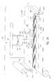
- FIG. 1is a schematic isometric view of a web-format planarizing machine 100 that has a support table 102 with a support surface 110 at a workstation defining a planarizing zone.
- the support surface 110is generally a rigid panel or plate attached to the table 102 to provide a flat, solid surface to which a portion of a web-format planarizing pad 140 is supported during planarization.
- the planarizing machine 100also has a plurality of rollers to guide, position, and hold the web-format pad 140 over the support surface 110 .
- the rollersgenerally include a supply roller 120 , first and second idler rollers 121 a and 121 b , first and second guide rollers 122 a and 122 b , and a take-up roller 123 .
- a motor(not shown) drives the take-up roller 123 , and possibly the supply roller 120 , to advance the pad 140 across the support surface 110 along a travel axis T—T.
- the first idler roller 121 a and the first guide roller 122 aalso stretch the pad 140 over the support surface 110 to hold the pad 140 during operation.
- the planarizing machine 100also has a carrier assembly 130 to translate a substrate assembly 12 across the pad 140 .
- the carrier assembly 130has a substrate assembly holder 132 to pick up, hold and release the substrate assembly 12 at appropriate stages of the planarizing process.
- the carrier assembly 130also has a support gantry 134 and a drive assembly 135 that can move along the gantry 134 .
- the drive assembly 135has an actuator 136 , a drive shaft 137 coupled to the actuator 136 , and an arm 138 projecting from the drive shaft 137 .
- the arm 138carries the substrate assembly holder 132 via another shaft 139 .
- the actuator 136orbits the substrate assembly holder 132 about an axis B—B to move the substrate assembly 12 across the pad 140 .
- the polishing pad 140may be a non-abrasive polymeric web (e.g., a polyurethane sheet), or it may be a fixed abrasive polishing pad having abrasive particles fixedly dispersed in a suspension medium.
- a planarizing fluid 144flows from a plurality of nozzles 145 .
- the planarizing fluid 144may be a conventional CMP slurry with abrasive particles and chemicals that etch and/or oxidize the substrate assembly 12 , or the planarizing fluid 144 may be a non-abrasive planarizing solution without abrasive particles. In most CMP applications, abrasive slurries are used on non-abrasive polishing pads, and non-abrasive planarizing solutions are used on fixed abrasive polishing pads.
- the planarizing machine 100incrementally moves the pad 140 across the support surface 110 either during or between planarizing cycles to change the particular portion of the polishing pad 140 in the planarizing zone.
- the supply and take-up rollers 120 and 123can drive the polishing pad 140 such that a point P moves incrementally across the support surface 110 to a number of intermediate locations I 1 , I 2 , etc.
- the rollers 120 and 123may drive the polishing pad 140 such that the point P moves all the way across the support surface 110 to completely remove a used portion of the pad 140 from the planarizing zone on the support surface 110 .
- the rollersmay also continuously drive the polishing pad at a slow rate such that the point P moves continuously across the support surface 110 .
- the polishing pad 140should be free to move axially over the length of the support surface 110 along the travel axis T—T.
- CMP processesshould consistently and accurately produce a uniform, planar surface on the substrate assembly to enable circuit and device patterns to be formed with photolithography techniques. As the density of integrated circuits increases, it is often necessary to accurately focus the critical dimensions of the photo-patterns to within a tolerance of approximately 0.1 ⁇ m. Focusing photo-patterns to such small tolerances, however, is difficult when the planarized surface of the wafer is not uniformly planar. Thus, CMP processes should create a highly uniform, planar surface to be effective.
- the polishing pad 140may move transversely to the travel axis T—T during a planarizing cycle of the substrate assembly 12 .
- the first idler roller 121 a and the first guide roller 122 astretch the pad 140 over the support surface 110
- the orbital motion of the substrate assembly 12 and the friction between the substrate assembly 12 and the pad 140may cause the pad 140 to move transverse to the travel axis T—T.
- Such transverse movement of the polishing pad 140can produce inconsistent planarizing results because it stretches and/or damages the polishing pad 140 .
- the transverse movement of the polishing pad 140may also allow the slurry to seep underneath the polishing pad 140 , which causes uneven wear of the pad 140 and contamination of the planarizing machine 200 . Moreover, if the pad wears unevenly, the topography of the pad may cause vibrations in the CMP machine that further affect the planarity of the finished surface and the consistency of the CMP process.
- a polishing pad for planarizing microelectronic-device substrate assemblieshas a first surface configured to engage a substrate assembly and a second surface configured to releasably engage the support surface of a planarizing machine.
- the second surface of the polishing padfor example, can have an interlocking element configured to engage a corresponding retaining member on the support surface to inhibit relative movement between the polishing pad and the support surface.
- the interlocking element and the retaining memberare configured so that the pad can move over the support surface along a travel path or axis, but relative movement between the pad and the support surface transverse to the travel axis is at least substantially inhibited.
- the interlocking element and the retaining membercan have several embodiments.
- the interlocking elementcan be an elongated tongue on the second surface of the polishing pad extending along the travel axis and the retaining member can be an elongated groove in the support surface.
- the interlocking element and the retaining membercan alternatively be another type of a protuberance and a reciprocal depression combination, such as elongated ridges or teeth extending along the travel axis.
- the support surfacecan further include one or more apertures coupled with a fluid pump to draw together or blow apart the interlocking elements and the retaining members.
- FIG. 1is a schematic isometric view of a web-format planarizing machine with a web-format polishing pad in accordance with the prior art.
- FIG. 2Ais a schematic isometric exploded view of a web-format planarizing machine including a sub-pad and a polishing pad having elongated ridges in accordance with an embodiment of the invention.
- FIG. 2Bis a partial cross-sectional isometric view of the polishing pad and the sub-pad of FIG. 2A along line 2 B— 2 B.
- FIG. 3Ais a schematic isometric exploded view of a web-format planarizing machine including a sub-pad having a plurality of teeth and a polishing pad having a plurality of reciprocal teeth in accordance with another embodiment of the invention.
- FIG. 3Bis a partial cross-sectional isometric view of the polishing pad and the sub-pad of FIG. 3A taken along line 3 B— 3 B.
- FIG. 4Ais a schematic isometric exploded view of a web-format planarizing machine including a sub-pad having depressions and a polishing pad having reciprocal protuberances in accordance with still another embodiment of the invention.
- FIGS. 4B and 4Care partial cross-sectional isometric views of alternative embodiments of the polishing pad and the sub-pad with depressions and reciprocal protuberances.
- FIG. 5Ais a schematic isometric exploded view of a web-format planarizing machine including a sub-pad having a groove and a polishing pad having a reciprocal tongue in accordance with yet another embodiment of the invention.
- FIGS. 5B and 5Care partial cross-sectional isometric views of alternative embodiments of the polishing pad and the sub-pad with grooves and reciprocal tongues.
- FIG. 6is a schematic isometric view of a web-format planarizing machine with a support surface having guide rails in accordance with still another embodiment of the invention.
- the present inventionis directed toward the methods and apparatuses for releasably engaging a polishing pad with a support surface of a planarizing machine to restrict movement of the polishing pad in mechanical and/or chemical-mechanical planarization of microelectronic-device substrate assemblies.
- Several embodiments of the inventionare directed toward polishing pads having interlocking elements that engage reciprocal retaining members on the support surface in a manner that restricts the pad from moving transversely to a travel axis but allows the pad to move along the travel axis.
- Many specific details of certain embodiments of the inventionare set forth in the following description and in FIGS. 2A-6 to provide a thorough understanding of such embodiments.
- One skilled in the art, however,will understand that the present invention may have additional embodiments, or that the invention may be practiced without several of the details described in the following description.
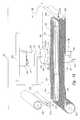
- FIG. 2Ais a schematic isometric view partially illustrating a web-format CMP apparatus 200 having a support surface 210 defined by an upper surface of a sub-pad 212 and a web-format polishing pad 240 in accordance with one embodiment of the invention.
- the planarizing machine 200may also have a carrier assembly 230 and a plurality of rollers for selectively moving the polishing pad 240 over the support surface 210 along a travel axis T—T.
- the carrier assembly 230 and the rollers 220 , 221 a , 221 b , 222 a , 222 b , and 223can be similar to those described above with reference to FIG. 1 .
- the support surface 210 and the polishing pad 240 of this embodimentinterlock with one another to allow the pad 240 to slide along the travel axis T—T, but to at least substantially inhibit the polishing pad 240 from moving transversely to the travel axis T—T during a planarizing cycle.
- “transverse”is defined as any non-parallel movement or configuration.
- FIG. 2Bis a partial cross-sectional view illustrating the polishing pad 240 and the support surface 210 of the sub-pad 212 in greater detail.
- the polishing pad 240 of this embodimenthas a body 241 with a planarizing surface 242 configured to engage the substrate assembly 12 and a backside surface 243 configured to engage the support surface 210 .
- the planarizing surface 242can be a highly planar surface, or it can have grooves, wells or other surface topographies to transport or hold a planarizing solution under the substrate assembly.
- the backside surface 243 of the pad 240can have at least one, and preferably a plurality, of interlocking elements 246 .
- the interlocking elements 246are elongated ridges extending along the backside 243 in a direction at least substantially parallel to the pad travel axis T—T.
- the support surface 210 of sub-pad 212can have at least one, and preferably a plurality, of retaining members 213 configured to releasably engage the interlocking elements 246 .
- the retaining members 213are elongated ridges extending along the support surface 210 to interlock with the interlocking elements 246 .
- the elongated ridges defining the interlocking elements 246 and the retaining members 213preferably have a plurality of alternating peaks 247 and troughs 248 with substantially similar dimensions.
- the peaks 247have a height of approximately 10-1000 ⁇ m. The representation of the peaks 247 and troughs 248 in FIG. 2, therefore, is exaggerated for purposes of illustration.
- the sub-pad 212interlocks with the polishing pad 240 to control the motion of the polishing pad 240 relative to the travel axis T—T.
- the sub-pad 212is preferably attached to a rigid, flat panel or plate 214 , such as a table.
- the sub-pad 212can be attached to the panel 214 with an adhesive, tape or other suitable compound typically used to adhere circular polishing pads to rotary planarizing machines.
- the fixed sub-pad 212at least substantially inhibits the polishing pad 240 from moving in a direction transverse to the travel axis T—T because the intermeshing of the elongated ridges 213 and the interlocking elements 246 impedes transverse movement between the sub-pad 212 and the pad 214 .
- the interlocking elements 246 and the retaining members 213allow the polishing pad 240 to move freely over the support surface 210 along the travel axis T—T.
- FIG. 2Abest illustrates an embodiment of planarizing the substrate assembly 12 with the planarizing apparatus 200 .
- the actuator 236orbits the substrate assembly holder 232 about the axis B—B to move the substrate assembly 12 across the pad 240 .
- the first idler roller 221 a and the first guide roller 222 astretch the polishing pad 240 over the sub-pad 212 to intermesh the interlocking elements 246 and the retaining members 213 .
- the actuator 236orbits the substrate assembly 12 across the polishing pad 240 , the interlocking elements 246 and the retaining members 213 impede the pad 240 from moving transversely to the travel axis T—T.
- the supply and take up rollers 220 and 223slide the polishing pad 240 over the sub-pad 212 along the travel axis T—T.
- the interlocking elements 246 and retaining members 213accordingly allow the pad 240 to move axially along the travel axis T—T because they extend at least substantially parallel to the travel axis T—T.
- planarizing apparatus 200is expected to prolong the pad life and provide consistent planarizing results. Unlike existing vacuum designs or adhesives, the planarizing apparatus 200 engages the interlocking elements 246 of the polishing pad 240 with the retaining members 213 of the sub-pad 212 to allow relative movement in a first direction (e.g., along the travel axis T—T) but to inhibit relative movement transverse to the first direction.
- a first directione.g., along the travel axis T—T
- One expected result of inhibiting such transverse movement of the polishing pad 240is to reduce wear or damage to the polishing pad 240 caused by stretching and/or twisting the pad transversely to the travel axis T—T.
- planarizing surface 242is expected to wear more evenly to produce more consistent planarizing results.
- Another expected result of inhibiting such transverse movement of the polishing pad 240is to reduce the volume of planarizing solution that seeps underneath the polishing pad 240 , which is expected to further reduce uneven wear of the pad and contamination of the planarizing machine 200 .
- the planarizing apparatus 200is expected to prolong the pad life and to more consistently planarize substrate assemblies.
- the polishing pad 240can be directly supported by the table 214 without the sub-pad 212 .
- the top surface of the table 214therefore, can have at least one, and preferably a plurality, of retaining members configured to releasably engage the interlocking elements of the polishing pad 240 .
- the retaining membersare elongated ridges extending along the table 214 similar to the retaining members 213 on the sub-pad. The polishing pad 240 can thus engage the top surface of the table 214 directly such that the support surface is defined by the top surface of the table 214 .
- FIG. 3Ais a schematic isometric view partially illustrating a web-format CMP apparatus 300 having a support surface 310 defined by an upper surface of a sub-pad 312 and a web-format polishing pad 340 in accordance with another embodiment of the invention.
- the planarizing machine 300may also have a carrier assembly 330 and a plurality of rollers for selectively moving the polishing pad 340 over the support surface 310 along a travel axis T—T.
- the support surface 310 and the polishing pad 340can interlock with one another to substantially inhibit the polishing pad 340 from moving in any direction during a planarizing cycle.
- FIG. 3Bis a partial cross-sectional view illustrating the polishing pad 340 and the support surface 310 of the sub-pad 312 in greater detail.
- polishing pad 340has a planarizing surface 342 configured to planarize a microelectronic-device substrate, a backside 343 opposite the planarizing surface 342 , and a plurality of pyramidal interlocking elements 344 projecting from the backside 343 .
- the support surface 310 of the sub-pad 312can have at least one, and preferably a plurality, of pyramidal retaining members 316 configured to releasably engage the interlocking elements 344 .
- the pyramidal interlocking elements 344 and retaining members 316preferably have a plurality of alternating peaks 347 and depressions 348 with substantially similar dimensions such that the depressions of one receives the peaks of the other.
- the pyramidal interlocking elements 344 and retaining members 316have a height from approximately 10-1000 ⁇ m, and more particularly from 30-50 ⁇ m. The representation of the interlocking elements 344 and the retaining members 316 in FIGS. 3A and 3B is thus exaggerated for purposes of illustration.
- the sub-pad 312interlocks with the polishing pad 340 to control the motion of the polishing pad 340 relative to the sub-pad 312 .
- the sub-pad 312is preferably attached to a rigid, flat panel or plate 314 , such as a table in a manner similar to that described above with reference to FIGS. 2A and 2B.
- the table 314 and the sub-pad 312may further include a plurality of fluid apertures 352 in fluid communication with a fluid passageway 354 .
- the fluid apertures 352may have a circular cross-sectional shape, comprise slots or have other shapes in other embodiments.
- the fluid passageway 354is connected to a conduit 358 that is in turn coupled to a pump 356 that can draw a fluid or blow a fluid through the passageway 354 .
- a liquid trapmay be positioned in the conduit 358 and apart from the base to separate liquid from the fluid drawn by the pump 356 .
- the liquid trap 359may form an integral component of the pump 356 .
- the polishing pad 340is rolled up on the supply roller 320 and one end is extended over the table 314 and attached to the take-up roller 323 .
- the pump 356draws a fluid against the backside 343 of the pad 340 to draw the polishing pad 340 tightly against the sub-pad 312 .
- the carrier assembly 330moves relative to the polishing pad 340 and presses the substrate 12 against the planarizing surface 342 to planarize the semiconductor substrate assembly 12 .
- the carrier assembly 330disengages the substrate assembly 12 from the pad 340 and the pump 356 reverses the flow to blow fluid through the passageway 354 .
- the positive pressure in the passageway 354disengages the interlocking elements 344 from the retaining member 316 so that the rollers 320 and 323 can advance the polishing pad 340 over the sub-pad 312 .
- the pump 356may draw the fluid against the pad 340 to reengage the interlocking elements 344 and the retaining members 316 .
- the pump 356can be replaced with a source of electrical current to apply a charge to the table 314 and attract the polishing pad 340 toward the table 314 via electrostatic forces.
- the polishing pad 340can include a conductive layer adjacent the table 314 , and in another aspect of this alternative embodiment the polishing pad 340 can include particles capable of receiving an induced electrostatic force.
- the polishing pad 340 and sub-pad 312can be cut in circular sheets for use on rotary planarizing machines, such as those disclosed in U.S. Pat. Nos. 5,486,131; 5,456,627; and 5,020,283, all of which are herein incorporated by reference.
- the CMP apparatus 300 shown in FIG. 3Acan securely engage the polishing pad 340 with the sub-pad 312 to prevent the pad 340 from wrinkling or folding when the semiconductor substrate assembly 12 is planarized.
- the CMP apparatus 300 shown in FIG. 3Aalso releasably attaches the polishing pad 340 to the sub-pad 312 without the need for tensioning the polishing pad 340 . Accordingly, the polishing pad 340 may be less likely to stretch or otherwise deform.
- FIG. 4Ais a schematic isometric view illustrating a web-format CMP apparatus 400 having a support surface 410 defined by an upper surface of a sub-pad 412 and a web-format polishing pad 440 in accordance with still another embodiment of the invention.
- the carrier assembly 430 and rollerscan be similar to those described above with reference to FIG. 1 .
- the support surface 410may also have a plurality of apertures (not shown) similar to those shown in FIG. 3A to draw a fluid to create a vacuum or blow the fluid to apply a positive pressure against the pad 440 .
- FIGS. 4B and 4Care partial cross-sectional views illustrating different aspects of the polishing pad 440 and the support surface 410 of the sub-pad 412 in greater detail.
- the support surface 410has a plurality of retaining members 416 defined by hemispherical depressions in the support surface 410 .
- the pad 440 in FIG. 4Bhas a flat planarizing surface 442 and a plurality of hemispherical interlocking elements 447 projecting from its backside.
- the planarizing surface 442 of the polishing pad 440 in FIG. 4Calso has a plurality of depressions to receive the interlocking elements 447 when the pad 440 is rolled on the supply and take up rollers 420 and 423 . In operation, the interlocking elements 447 mate with the retaining members 416 to inhibit relative movement between the pad 440 and the sub-pad 412 .
- FIG. 5Ais a schematic isometric view illustrating a web-format CMP apparatus 500 having a support surface 510 defined by an upper surface of a sub-pad 512 and a web-format polishing pad 540 in accordance with yet another embodiment of the invention.
- the carrier assembly 530 and rollerscan be similar to those described above with reference to FIG. 1 .
- FIGS. 5B and 5Care partial cross-sectional views illustrating different aspects of the polishing pad 540 and the sub-pad 512 in greater detail.
- the support surface 510 of FIG. 5Bhas a plurality of retaining members 518 defined by elongated tongues extending in the direction of the travel path T—T.
- the polishing pad 540 of FIG. 5Bhas a flat planarizing surface 542 and a backside 543 with a plurality of interlocking elements 548 defined by elongated grooves.
- the sub-pad 512 and polishing pad 540 of FIG. 5Chave an inverse tongue and groove arrangement from FIG. 5 B.
- the polishing pad 540has at least one interlocking element 548 that is an elongated tongue configured to fit in a groove type retaining member 518 .
- the planarizing surface 542 of the pad 540 shown in FIG. 5Calso has at least one groove indentation 549 to receive a corresponding interlocking element 548 when the pad is rolled-up on the rollers 520 and 523 .
- the sub-pad 512interlocks with the polishing pad 540 to control the motion of the polishing pad 540 relative to the sub-pad 512 .
- the sub-pad 512is preferably attached to a rigid, flat panel or plate 514 , such as a table in a manner similar to that described with reference to FIGS. 2A and 2B.
- the table 514has at least one retaining member 518 , such as an elongated groove or tongue, that interlocks with the interlocking element 548 to inhibit relative movement between the pad 540 and the table 514 transverse to the travel path T—T.
- FIG. 6is a schematic isometric view of a web-format CMP apparatus 600 having a support surface 610 , a sub-pad 612 , and a web-format polishing pad 640 similar to those described above with reference to FIG. 1 .
- the supply rollers 620 and the take up rollers 623may provide a positive tension on the polishing pad 640 in the direction of travel T—T.
- a guide wall 650projects upwardly from each edge of the support surface 610 and extends substantially parallel to the direction of travel T—T.
- the guide walls 650generally have a height above the thickness of the polishing pad 640 and are generally spaced apart the width of the polishing pad 640 .
- the guide walls 650permit the web-format polishing pad 640 to move freely in the direction of travel T—T, but inhibit the polishing pad 640 from moving transversely to the direction of travel path T—T.
- the fluid pump components of FIG. 3Acan be combined with any one of the above embodiments to engage the interlocking surfaces prior to planarization or to disengage the interlocking surfaces upon completion of the planarization cycle.
- the guide walls 650 of FIG. 6can be combined with any one of the above embodiments to further restrict transverse movement of the polishing pad relative to the travel path T—T.
Landscapes
- Engineering & Computer Science (AREA)
- Mechanical Engineering (AREA)
- Finish Polishing, Edge Sharpening, And Grinding By Specific Grinding Devices (AREA)
- Mechanical Treatment Of Semiconductor (AREA)
Abstract
Description
Claims (24)
Priority Applications (1)
| Application Number | Priority Date | Filing Date | Title |
|---|---|---|---|
| US09/696,336US6439970B1 (en) | 1999-04-02 | 2000-10-24 | Method and apparatus for releasably attaching polishing pads to planarizing machines in mechanical and/or chemical-mechanical planarization of microelectronic-device substrate assemblies |
Applications Claiming Priority (2)
| Application Number | Priority Date | Filing Date | Title |
|---|---|---|---|
| US09/285,319US6296557B1 (en) | 1999-04-02 | 1999-04-02 | Method and apparatus for releasably attaching polishing pads to planarizing machines in mechanical and/or chemical-mechanical planarization of microelectronic-device substrate assemblies |
| US09/696,336US6439970B1 (en) | 1999-04-02 | 2000-10-24 | Method and apparatus for releasably attaching polishing pads to planarizing machines in mechanical and/or chemical-mechanical planarization of microelectronic-device substrate assemblies |
Related Parent Applications (1)
| Application Number | Title | Priority Date | Filing Date |
|---|---|---|---|
| US09/285,319DivisionUS6296557B1 (en) | 1999-04-02 | 1999-04-02 | Method and apparatus for releasably attaching polishing pads to planarizing machines in mechanical and/or chemical-mechanical planarization of microelectronic-device substrate assemblies |
Publications (1)
| Publication Number | Publication Date |
|---|---|
| US6439970B1true US6439970B1 (en) | 2002-08-27 |
Family
ID=23093722
Family Applications (3)
| Application Number | Title | Priority Date | Filing Date |
|---|---|---|---|
| US09/285,319Expired - Fee RelatedUS6296557B1 (en) | 1999-04-02 | 1999-04-02 | Method and apparatus for releasably attaching polishing pads to planarizing machines in mechanical and/or chemical-mechanical planarization of microelectronic-device substrate assemblies |
| US09/696,336Expired - LifetimeUS6439970B1 (en) | 1999-04-02 | 2000-10-24 | Method and apparatus for releasably attaching polishing pads to planarizing machines in mechanical and/or chemical-mechanical planarization of microelectronic-device substrate assemblies |
| US09/696,335Expired - LifetimeUS6416616B1 (en) | 1999-04-02 | 2000-10-24 | Apparatus for releasably attaching polishing pads to planarizing machines in mechanical and/or chemical-mechanical planarization of microelectronic-device substrate assemblies |
Family Applications Before (1)
| Application Number | Title | Priority Date | Filing Date |
|---|---|---|---|
| US09/285,319Expired - Fee RelatedUS6296557B1 (en) | 1999-04-02 | 1999-04-02 | Method and apparatus for releasably attaching polishing pads to planarizing machines in mechanical and/or chemical-mechanical planarization of microelectronic-device substrate assemblies |
Family Applications After (1)
| Application Number | Title | Priority Date | Filing Date |
|---|---|---|---|
| US09/696,335Expired - LifetimeUS6416616B1 (en) | 1999-04-02 | 2000-10-24 | Apparatus for releasably attaching polishing pads to planarizing machines in mechanical and/or chemical-mechanical planarization of microelectronic-device substrate assemblies |
Country Status (1)
| Country | Link |
|---|---|
| US (3) | US6296557B1 (en) |
Cited By (1)
| Publication number | Priority date | Publication date | Assignee | Title |
|---|---|---|---|---|
| US20040053562A1 (en)* | 2002-07-12 | 2004-03-18 | Angela Petroski | Method for securing a polishing pad to a platen for use in chemical-mechanical polishing of wafers |
Families Citing this family (61)
| Publication number | Priority date | Publication date | Assignee | Title |
|---|---|---|---|---|
| US6075606A (en) | 1996-02-16 | 2000-06-13 | Doan; Trung T. | Endpoint detector and method for measuring a change in wafer thickness in chemical-mechanical polishing of semiconductor wafers and other microelectronic substrates |
| CN1345264A (en)* | 1999-03-30 | 2002-04-17 | 株式会社尼康 | Polishing disk, polishing machine, polishing method and method for manufacturing semiconductor device |
| US6296557B1 (en) | 1999-04-02 | 2001-10-02 | Micron Technology, Inc. | Method and apparatus for releasably attaching polishing pads to planarizing machines in mechanical and/or chemical-mechanical planarization of microelectronic-device substrate assemblies |
| EP1052062A1 (en) | 1999-05-03 | 2000-11-15 | Applied Materials, Inc. | Pré-conditioning fixed abrasive articles |
| US6722963B1 (en)* | 1999-08-03 | 2004-04-20 | Micron Technology, Inc. | Apparatus for chemical-mechanical planarization of microelectronic substrates with a carrier and membrane |
| US6273796B1 (en) | 1999-09-01 | 2001-08-14 | Micron Technology, Inc. | Method and apparatus for planarizing a microelectronic substrate with a tilted planarizing surface |
| US6383934B1 (en) | 1999-09-02 | 2002-05-07 | Micron Technology, Inc. | Method and apparatus for chemical-mechanical planarization of microelectronic substrates with selected planarizing liquids |
| US6520843B1 (en)* | 1999-10-27 | 2003-02-18 | Strasbaugh | High planarity chemical mechanical planarization |
| US6306768B1 (en) | 1999-11-17 | 2001-10-23 | Micron Technology, Inc. | Method for planarizing microelectronic substrates having apertures |
| US7077721B2 (en) | 2000-02-17 | 2006-07-18 | Applied Materials, Inc. | Pad assembly for electrochemical mechanical processing |
| US7029365B2 (en) | 2000-02-17 | 2006-04-18 | Applied Materials Inc. | Pad assembly for electrochemical mechanical processing |
| US6848970B2 (en) | 2002-09-16 | 2005-02-01 | Applied Materials, Inc. | Process control in electrochemically assisted planarization |
| US7303662B2 (en) | 2000-02-17 | 2007-12-04 | Applied Materials, Inc. | Contacts for electrochemical processing |
| US6979248B2 (en) | 2002-05-07 | 2005-12-27 | Applied Materials, Inc. | Conductive polishing article for electrochemical mechanical polishing |
| US7303462B2 (en) | 2000-02-17 | 2007-12-04 | Applied Materials, Inc. | Edge bead removal by an electro polishing process |
| US6991528B2 (en) | 2000-02-17 | 2006-01-31 | Applied Materials, Inc. | Conductive polishing article for electrochemical mechanical polishing |
| US7678245B2 (en) | 2000-02-17 | 2010-03-16 | Applied Materials, Inc. | Method and apparatus for electrochemical mechanical processing |
| US7059948B2 (en)* | 2000-12-22 | 2006-06-13 | Applied Materials | Articles for polishing semiconductor substrates |
| US7374644B2 (en) | 2000-02-17 | 2008-05-20 | Applied Materials, Inc. | Conductive polishing article for electrochemical mechanical polishing |
| US7670468B2 (en) | 2000-02-17 | 2010-03-02 | Applied Materials, Inc. | Contact assembly and method for electrochemical mechanical processing |
| US6962524B2 (en) | 2000-02-17 | 2005-11-08 | Applied Materials, Inc. | Conductive polishing article for electrochemical mechanical polishing |
| US7125477B2 (en) | 2000-02-17 | 2006-10-24 | Applied Materials, Inc. | Contacts for electrochemical processing |
| US6498101B1 (en) | 2000-02-28 | 2002-12-24 | Micron Technology, Inc. | Planarizing pads, planarizing machines and methods for making and using planarizing pads in mechanical and chemical-mechanical planarization of microelectronic device substrate assemblies |
| US6706139B1 (en)* | 2000-04-19 | 2004-03-16 | Micron Technology, Inc. | Method and apparatus for cleaning a web-based chemical mechanical planarization system |
| US6313038B1 (en) | 2000-04-26 | 2001-11-06 | Micron Technology, Inc. | Method and apparatus for controlling chemical interactions during planarization of microelectronic substrates |
| US6612901B1 (en) | 2000-06-07 | 2003-09-02 | Micron Technology, Inc. | Apparatus for in-situ optical endpointing of web-format planarizing machines in mechanical or chemical-mechanical planarization of microelectronic-device substrate assemblies |
| US6500056B1 (en)* | 2000-06-30 | 2002-12-31 | Lam Research Corporation | Linear reciprocating disposable belt polishing method and apparatus |
| US6495464B1 (en)* | 2000-06-30 | 2002-12-17 | Lam Research Corporation | Method and apparatus for fixed abrasive substrate preparation and use in a cluster CMP tool |
| US6520834B1 (en) | 2000-08-09 | 2003-02-18 | Micron Technology, Inc. | Methods and apparatuses for analyzing and controlling performance parameters in mechanical and chemical-mechanical planarization of microelectronic substrates |
| US6838382B1 (en) | 2000-08-28 | 2005-01-04 | Micron Technology, Inc. | Method and apparatus for forming a planarizing pad having a film and texture elements for planarization of microelectronic substrates |
| US6736869B1 (en) | 2000-08-28 | 2004-05-18 | Micron Technology, Inc. | Method for forming a planarizing pad for planarization of microelectronic substrates |
| US6592443B1 (en) | 2000-08-30 | 2003-07-15 | Micron Technology, Inc. | Method and apparatus for forming and using planarizing pads for mechanical and chemical-mechanical planarization of microelectronic substrates |
| US6609947B1 (en) | 2000-08-30 | 2003-08-26 | Micron Technology, Inc. | Planarizing machines and control systems for mechanical and/or chemical-mechanical planarization of micro electronic substrates |
| US6652764B1 (en) | 2000-08-31 | 2003-11-25 | Micron Technology, Inc. | Methods and apparatuses for making and using planarizing pads for mechanical and chemical-mechanical planarization of microelectronic substrates |
| US7077733B1 (en)* | 2000-08-31 | 2006-07-18 | Micron Technology, Inc. | Subpad support with a releasable subpad securing element and polishing apparatus including the subpad support |
| US6623329B1 (en) | 2000-08-31 | 2003-09-23 | Micron Technology, Inc. | Method and apparatus for supporting a microelectronic substrate relative to a planarization pad |
| US6475332B1 (en)* | 2000-10-05 | 2002-11-05 | Lam Research Corporation | Interlocking chemical mechanical polishing system |
| US7137879B2 (en) | 2001-04-24 | 2006-11-21 | Applied Materials, Inc. | Conductive polishing article for electrochemical mechanical polishing |
| US7344432B2 (en) | 2001-04-24 | 2008-03-18 | Applied Materials, Inc. | Conductive pad with ion exchange membrane for electrochemical mechanical polishing |
| US6722943B2 (en)* | 2001-08-24 | 2004-04-20 | Micron Technology, Inc. | Planarizing machines and methods for dispensing planarizing solutions in the processing of microelectronic workpieces |
| US6866566B2 (en) | 2001-08-24 | 2005-03-15 | Micron Technology, Inc. | Apparatus and method for conditioning a contact surface of a processing pad used in processing microelectronic workpieces |
| US6666749B2 (en) | 2001-08-30 | 2003-12-23 | Micron Technology, Inc. | Apparatus and method for enhanced processing of microelectronic workpieces |
| US20030047044A1 (en)* | 2001-09-07 | 2003-03-13 | Jose Porchia | Processing method using a film material |
| US20030224678A1 (en)* | 2002-05-31 | 2003-12-04 | Applied Materials, Inc. | Web pad design for chemical mechanical polishing |
| US8602851B2 (en)* | 2003-06-09 | 2013-12-10 | Rohm And Haas Electronic Materials Cmp Holdings, Inc. | Controlled penetration subpad |
| US6638391B1 (en)* | 2002-06-19 | 2003-10-28 | United Microelectronics Corp. | Wafer carrier assembly for a chemical mechanical polishing apparatus and a polishing method using the same |
| US7341502B2 (en) | 2002-07-18 | 2008-03-11 | Micron Technology, Inc. | Methods and systems for planarizing workpieces, e.g., microelectronic workpieces |
| US6884152B2 (en) | 2003-02-11 | 2005-04-26 | Micron Technology, Inc. | Apparatuses and methods for conditioning polishing pads used in polishing micro-device workpieces |
| US6935929B2 (en) | 2003-04-28 | 2005-08-30 | Micron Technology, Inc. | Polishing machines including under-pads and methods for mechanical and/or chemical-mechanical polishing of microfeature workpieces |
| US7030603B2 (en) | 2003-08-21 | 2006-04-18 | Micron Technology, Inc. | Apparatuses and methods for monitoring rotation of a conductive microfeature workpiece |
| US7135124B2 (en) | 2003-11-13 | 2006-11-14 | International Business Machines Corporation | Method for thinning wafers that have contact bumps |
| US7066792B2 (en) | 2004-08-06 | 2006-06-27 | Micron Technology, Inc. | Shaped polishing pads for beveling microfeature workpiece edges, and associate system and methods |
| US7520968B2 (en) | 2004-10-05 | 2009-04-21 | Applied Materials, Inc. | Conductive pad design modification for better wafer-pad contact |
| US7427340B2 (en) | 2005-04-08 | 2008-09-23 | Applied Materials, Inc. | Conductive pad |
| US7264539B2 (en) | 2005-07-13 | 2007-09-04 | Micron Technology, Inc. | Systems and methods for removing microfeature workpiece surface defects |
| US7294049B2 (en) | 2005-09-01 | 2007-11-13 | Micron Technology, Inc. | Method and apparatus for removing material from microfeature workpieces |
| KR100882045B1 (en)* | 2006-02-15 | 2009-02-09 | 어플라이드 머티어리얼스, 인코포레이티드 | Polishing apparatus with grooved subpad |
| US8968055B2 (en)* | 2012-04-28 | 2015-03-03 | Applied Materials, Inc. | Methods and apparatus for pre-chemical mechanical planarization buffing module |
| JP2023537084A (en)* | 2020-08-10 | 2023-08-30 | スリーエム イノベイティブ プロパティズ カンパニー | Polishing system and method of use |
| US20250091094A1 (en)* | 2023-09-20 | 2025-03-20 | Applied Materials, Inc. | Backflush seal cleaning apparatus |
| US20250141459A1 (en) | 2023-10-26 | 2025-05-01 | Analog Devices International Unlimited Company | Configurable digital-to-analog converter calibration |
Citations (25)
| Publication number | Priority date | Publication date | Assignee | Title |
|---|---|---|---|---|
| US3408705A (en)* | 1966-07-07 | 1968-11-05 | Minnesota Mining & Mfg | Fastener articles |
| US3522681A (en)* | 1968-12-18 | 1970-08-04 | Gerald Lampert | Rubbing apparatus |
| US3695131A (en) | 1970-11-09 | 1972-10-03 | Ampex | Method of and apparatus for slitting webs |
| US3869764A (en)* | 1972-02-29 | 1975-03-11 | Int Fastener Ets | Press-on and split-off type fastener and manufacturing device therefor |
| US3918220A (en) | 1973-08-09 | 1975-11-11 | Ryton Mach Tools Coventry Ltd | Method of grinding a surface of a workpiece and a tool for carrying out the method |
| US3955245A (en)* | 1972-03-24 | 1976-05-11 | Gene Ballin | Separable interlocking fasteners |
| US4263755A (en)* | 1979-10-12 | 1981-04-28 | Jack Globus | Abrasive product |
| US4609581A (en)* | 1985-04-15 | 1986-09-02 | Minnesota Mining And Manufacturing Company | Coated abrasive sheet material with loop attachment means |
| US4617767A (en) | 1985-01-14 | 1986-10-21 | Ali Frank F | Sanding, buffing and polishing tool and parts thereof |
| US4875259A (en)* | 1986-09-08 | 1989-10-24 | Minnesota Mining And Manufacturing Company | Intermeshable article |
| US5097570A (en)* | 1991-01-23 | 1992-03-24 | Bruce Gershenson | Fastening system |
| US5201101A (en)* | 1992-04-28 | 1993-04-13 | Minnesota Mining And Manufacturing Company | Method of attaching articles and a pair of articles fastened by the method |
| US5201785A (en) | 1991-05-10 | 1993-04-13 | Minnesota Mining & Manufacturing Company | Disc-holder assembly |
| EP0706855A2 (en) | 1994-10-11 | 1996-04-17 | Ontrak Systems, Inc. | Wafer polishing machine |
| EP0774323A2 (en) | 1995-10-27 | 1997-05-21 | Applied Materials, Inc. | Apparatus and method for polishing substrates |
| US5672186A (en)* | 1994-01-13 | 1997-09-30 | Minnesota Mining And Manufacturing Company | Method of making an abrasive article |
| US5722877A (en)* | 1996-10-11 | 1998-03-03 | Lam Research Corporation | Technique for improving within-wafer non-uniformity of material removal for performing CMP |
| US5735731A (en)* | 1995-08-07 | 1998-04-07 | Samsung Electronics Co., Ltd. | Wafer polishing device |
| US5876268A (en) | 1997-01-03 | 1999-03-02 | Minnesota Mining And Manufacturing Company | Method and article for the production of optical quality surfaces on glass |
| US5958794A (en) | 1995-09-22 | 1999-09-28 | Minnesota Mining And Manufacturing Company | Method of modifying an exposed surface of a semiconductor wafer |
| US6007407A (en) | 1996-08-08 | 1999-12-28 | Minnesota Mining And Manufacturing Company | Abrasive construction for semiconductor wafer modification |
| US6036586A (en) | 1998-07-29 | 2000-03-14 | Micron Technology, Inc. | Apparatus and method for reducing removal forces for CMP pads |
| US6099603A (en)* | 1998-12-29 | 2000-08-08 | Johnson Abrasive Company, Inc. | System and method of attaching abrasive articles to backing pads |
| US6261168B1 (en) | 1999-05-21 | 2001-07-17 | Lam Research Corporation | Chemical mechanical planarization or polishing pad with sections having varied groove patterns |
| US6296557B1 (en) | 1999-04-02 | 2001-10-02 | Micron Technology, Inc. | Method and apparatus for releasably attaching polishing pads to planarizing machines in mechanical and/or chemical-mechanical planarization of microelectronic-device substrate assemblies |
- 1999
- 1999-04-02USUS09/285,319patent/US6296557B1/ennot_activeExpired - Fee Related
- 2000
- 2000-10-24USUS09/696,336patent/US6439970B1/ennot_activeExpired - Lifetime
- 2000-10-24USUS09/696,335patent/US6416616B1/ennot_activeExpired - Lifetime
Patent Citations (25)
| Publication number | Priority date | Publication date | Assignee | Title |
|---|---|---|---|---|
| US3408705A (en)* | 1966-07-07 | 1968-11-05 | Minnesota Mining & Mfg | Fastener articles |
| US3522681A (en)* | 1968-12-18 | 1970-08-04 | Gerald Lampert | Rubbing apparatus |
| US3695131A (en) | 1970-11-09 | 1972-10-03 | Ampex | Method of and apparatus for slitting webs |
| US3869764A (en)* | 1972-02-29 | 1975-03-11 | Int Fastener Ets | Press-on and split-off type fastener and manufacturing device therefor |
| US3955245A (en)* | 1972-03-24 | 1976-05-11 | Gene Ballin | Separable interlocking fasteners |
| US3918220A (en) | 1973-08-09 | 1975-11-11 | Ryton Mach Tools Coventry Ltd | Method of grinding a surface of a workpiece and a tool for carrying out the method |
| US4263755A (en)* | 1979-10-12 | 1981-04-28 | Jack Globus | Abrasive product |
| US4617767A (en) | 1985-01-14 | 1986-10-21 | Ali Frank F | Sanding, buffing and polishing tool and parts thereof |
| US4609581A (en)* | 1985-04-15 | 1986-09-02 | Minnesota Mining And Manufacturing Company | Coated abrasive sheet material with loop attachment means |
| US4875259A (en)* | 1986-09-08 | 1989-10-24 | Minnesota Mining And Manufacturing Company | Intermeshable article |
| US5097570A (en)* | 1991-01-23 | 1992-03-24 | Bruce Gershenson | Fastening system |
| US5201785A (en) | 1991-05-10 | 1993-04-13 | Minnesota Mining & Manufacturing Company | Disc-holder assembly |
| US5201101A (en)* | 1992-04-28 | 1993-04-13 | Minnesota Mining And Manufacturing Company | Method of attaching articles and a pair of articles fastened by the method |
| US5672186A (en)* | 1994-01-13 | 1997-09-30 | Minnesota Mining And Manufacturing Company | Method of making an abrasive article |
| EP0706855A2 (en) | 1994-10-11 | 1996-04-17 | Ontrak Systems, Inc. | Wafer polishing machine |
| US5735731A (en)* | 1995-08-07 | 1998-04-07 | Samsung Electronics Co., Ltd. | Wafer polishing device |
| US5958794A (en) | 1995-09-22 | 1999-09-28 | Minnesota Mining And Manufacturing Company | Method of modifying an exposed surface of a semiconductor wafer |
| EP0774323A2 (en) | 1995-10-27 | 1997-05-21 | Applied Materials, Inc. | Apparatus and method for polishing substrates |
| US6007407A (en) | 1996-08-08 | 1999-12-28 | Minnesota Mining And Manufacturing Company | Abrasive construction for semiconductor wafer modification |
| US5722877A (en)* | 1996-10-11 | 1998-03-03 | Lam Research Corporation | Technique for improving within-wafer non-uniformity of material removal for performing CMP |
| US5876268A (en) | 1997-01-03 | 1999-03-02 | Minnesota Mining And Manufacturing Company | Method and article for the production of optical quality surfaces on glass |
| US6036586A (en) | 1998-07-29 | 2000-03-14 | Micron Technology, Inc. | Apparatus and method for reducing removal forces for CMP pads |
| US6099603A (en)* | 1998-12-29 | 2000-08-08 | Johnson Abrasive Company, Inc. | System and method of attaching abrasive articles to backing pads |
| US6296557B1 (en) | 1999-04-02 | 2001-10-02 | Micron Technology, Inc. | Method and apparatus for releasably attaching polishing pads to planarizing machines in mechanical and/or chemical-mechanical planarization of microelectronic-device substrate assemblies |
| US6261168B1 (en) | 1999-05-21 | 2001-07-17 | Lam Research Corporation | Chemical mechanical planarization or polishing pad with sections having varied groove patterns |
Cited By (2)
| Publication number | Priority date | Publication date | Assignee | Title |
|---|---|---|---|---|
| US20040053562A1 (en)* | 2002-07-12 | 2004-03-18 | Angela Petroski | Method for securing a polishing pad to a platen for use in chemical-mechanical polishing of wafers |
| US6964601B2 (en) | 2002-07-12 | 2005-11-15 | Raytech Innovative Solutions, Llc | Method for securing a polishing pad to a platen for use in chemical-mechanical polishing of wafers |
Also Published As
| Publication number | Publication date |
|---|---|
| US6416616B1 (en) | 2002-07-09 |
| US6296557B1 (en) | 2001-10-02 |
Similar Documents
| Publication | Publication Date | Title |
|---|---|---|
| US6439970B1 (en) | Method and apparatus for releasably attaching polishing pads to planarizing machines in mechanical and/or chemical-mechanical planarization of microelectronic-device substrate assemblies | |
| US7138072B2 (en) | Methods and apparatuses for planarizing microelectronic substrate assemblies | |
| US6620032B2 (en) | Polishing pads and planarizing machines for mechanical and/or chemical-mechanical planarization of microelectronic substrate assemblies | |
| US6929530B1 (en) | Apparatus for in-situ optical endpointing on web-format planarizing machines in mechanical or chemical-mechanical planarization of microelectronic-device substrate assemblies and methods for making and using same | |
| US6913519B2 (en) | Method and apparatus for mechanical and chemical-mechanical planarization of microelectronic substrates | |
| US6358127B1 (en) | Method and apparatus for planarizing and cleaning microelectronic substrates | |
| CN101244535A (en) | Polishing warehouse | |
| US6852017B2 (en) | Method and apparatus for chemical-mechanical planarization of microelectronic substrates with a carrier and membrane | |
| US6540595B1 (en) | Chemical-Mechanical polishing apparatus and method utilizing an advanceable polishing sheet | |
| US6780095B1 (en) | Method and apparatus for mechanical and chemical-mechanical planarization of microelectronic substrates |
Legal Events
| Date | Code | Title | Description |
|---|---|---|---|
| FEPP | Fee payment procedure | Free format text:PAYOR NUMBER ASSIGNED (ORIGINAL EVENT CODE: ASPN); ENTITY STATUS OF PATENT OWNER: LARGE ENTITY | |
| STCF | Information on status: patent grant | Free format text:PATENTED CASE | |
| FPAY | Fee payment | Year of fee payment:4 | |
| FPAY | Fee payment | Year of fee payment:8 | |
| FPAY | Fee payment | Year of fee payment:12 | |
| AS | Assignment | Owner name:U.S. BANK NATIONAL ASSOCIATION, AS COLLATERAL AGENT, CALIFORNIA Free format text:SECURITY INTEREST;ASSIGNOR:MICRON TECHNOLOGY, INC.;REEL/FRAME:038669/0001 Effective date:20160426 Owner name:U.S. BANK NATIONAL ASSOCIATION, AS COLLATERAL AGEN Free format text:SECURITY INTEREST;ASSIGNOR:MICRON TECHNOLOGY, INC.;REEL/FRAME:038669/0001 Effective date:20160426 | |
| AS | Assignment | Owner name:MORGAN STANLEY SENIOR FUNDING, INC., AS COLLATERAL AGENT, MARYLAND Free format text:PATENT SECURITY AGREEMENT;ASSIGNOR:MICRON TECHNOLOGY, INC.;REEL/FRAME:038954/0001 Effective date:20160426 Owner name:MORGAN STANLEY SENIOR FUNDING, INC., AS COLLATERAL Free format text:PATENT SECURITY AGREEMENT;ASSIGNOR:MICRON TECHNOLOGY, INC.;REEL/FRAME:038954/0001 Effective date:20160426 | |
| AS | Assignment | Owner name:U.S. BANK NATIONAL ASSOCIATION, AS COLLATERAL AGENT, CALIFORNIA Free format text:CORRECTIVE ASSIGNMENT TO CORRECT THE REPLACE ERRONEOUSLY FILED PATENT #7358718 WITH THE CORRECT PATENT #7358178 PREVIOUSLY RECORDED ON REEL 038669 FRAME 0001. ASSIGNOR(S) HEREBY CONFIRMS THE SECURITY INTEREST;ASSIGNOR:MICRON TECHNOLOGY, INC.;REEL/FRAME:043079/0001 Effective date:20160426 Owner name:U.S. BANK NATIONAL ASSOCIATION, AS COLLATERAL AGEN Free format text:CORRECTIVE ASSIGNMENT TO CORRECT THE REPLACE ERRONEOUSLY FILED PATENT #7358718 WITH THE CORRECT PATENT #7358178 PREVIOUSLY RECORDED ON REEL 038669 FRAME 0001. ASSIGNOR(S) HEREBY CONFIRMS THE SECURITY INTEREST;ASSIGNOR:MICRON TECHNOLOGY, INC.;REEL/FRAME:043079/0001 Effective date:20160426 | |
| AS | Assignment | Owner name:JPMORGAN CHASE BANK, N.A., AS COLLATERAL AGENT, ILLINOIS Free format text:SECURITY INTEREST;ASSIGNORS:MICRON TECHNOLOGY, INC.;MICRON SEMICONDUCTOR PRODUCTS, INC.;REEL/FRAME:047540/0001 Effective date:20180703 Owner name:JPMORGAN CHASE BANK, N.A., AS COLLATERAL AGENT, IL Free format text:SECURITY INTEREST;ASSIGNORS:MICRON TECHNOLOGY, INC.;MICRON SEMICONDUCTOR PRODUCTS, INC.;REEL/FRAME:047540/0001 Effective date:20180703 | |
| AS | Assignment | Owner name:MICRON TECHNOLOGY, INC., IDAHO Free format text:RELEASE BY SECURED PARTY;ASSIGNOR:U.S. BANK NATIONAL ASSOCIATION, AS COLLATERAL AGENT;REEL/FRAME:047243/0001 Effective date:20180629 | |
| AS | Assignment | Owner name:MICRON TECHNOLOGY, INC., IDAHO Free format text:RELEASE BY SECURED PARTY;ASSIGNOR:MORGAN STANLEY SENIOR FUNDING, INC., AS COLLATERAL AGENT;REEL/FRAME:050937/0001 Effective date:20190731 | |
| AS | Assignment | Owner name:MICRON TECHNOLOGY, INC., IDAHO Free format text:RELEASE BY SECURED PARTY;ASSIGNOR:JPMORGAN CHASE BANK, N.A., AS COLLATERAL AGENT;REEL/FRAME:051028/0001 Effective date:20190731 Owner name:MICRON SEMICONDUCTOR PRODUCTS, INC., IDAHO Free format text:RELEASE BY SECURED PARTY;ASSIGNOR:JPMORGAN CHASE BANK, N.A., AS COLLATERAL AGENT;REEL/FRAME:051028/0001 Effective date:20190731 |