US6439898B2 - Method and apparatus for interconnecting devices using an adhesive - Google Patents
Method and apparatus for interconnecting devices using an adhesiveDownload PDFInfo
- Publication number
- US6439898B2 US6439898B2US09/794,101US79410101AUS6439898B2US 6439898 B2US6439898 B2US 6439898B2US 79410101 AUS79410101 AUS 79410101AUS 6439898 B2US6439898 B2US 6439898B2
- Authority
- US
- United States
- Prior art keywords
- contact
- contact structure
- devices
- electrical contact
- spring contact
- Prior art date
- Legal status (The legal status is an assumption and is not a legal conclusion. Google has not performed a legal analysis and makes no representation as to the accuracy of the status listed.)
- Expired - Lifetime, expires
Links
Images


Classifications
- H—ELECTRICITY
- H05—ELECTRIC TECHNIQUES NOT OTHERWISE PROVIDED FOR
- H05K—PRINTED CIRCUITS; CASINGS OR CONSTRUCTIONAL DETAILS OF ELECTRIC APPARATUS; MANUFACTURE OF ASSEMBLAGES OF ELECTRICAL COMPONENTS
- H05K3/00—Apparatus or processes for manufacturing printed circuits
- H05K3/30—Assembling printed circuits with electric components, e.g. with resistor
- H05K3/32—Assembling printed circuits with electric components, e.g. with resistor electrically connecting electric components or wires to printed circuits
- H05K3/325—Assembling printed circuits with electric components, e.g. with resistor electrically connecting electric components or wires to printed circuits by abutting or pinching, i.e. without alloying process; mechanical auxiliary parts therefor
- H—ELECTRICITY
- H01—ELECTRIC ELEMENTS
- H01L—SEMICONDUCTOR DEVICES NOT COVERED BY CLASS H10
- H01L21/00—Processes or apparatus adapted for the manufacture or treatment of semiconductor or solid state devices or of parts thereof
- H01L21/02—Manufacture or treatment of semiconductor devices or of parts thereof
- H01L21/04—Manufacture or treatment of semiconductor devices or of parts thereof the devices having potential barriers, e.g. a PN junction, depletion layer or carrier concentration layer
- H01L21/50—Assembly of semiconductor devices using processes or apparatus not provided for in a single one of the groups H01L21/18 - H01L21/326 or H10D48/04 - H10D48/07 e.g. sealing of a cap to a base of a container
- H01L21/56—Encapsulations, e.g. encapsulation layers, coatings
- H01L21/563—Encapsulation of active face of flip-chip device, e.g. underfilling or underencapsulation of flip-chip, encapsulation preform on chip or mounting substrate
- H—ELECTRICITY
- H01—ELECTRIC ELEMENTS
- H01L—SEMICONDUCTOR DEVICES NOT COVERED BY CLASS H10
- H01L24/00—Arrangements for connecting or disconnecting semiconductor or solid-state bodies; Methods or apparatus related thereto
- H01L24/01—Means for bonding being attached to, or being formed on, the surface to be connected, e.g. chip-to-package, die-attach, "first-level" interconnects; Manufacturing methods related thereto
- H01L24/10—Bump connectors ; Manufacturing methods related thereto
- H01L24/12—Structure, shape, material or disposition of the bump connectors prior to the connecting process
- H01L24/13—Structure, shape, material or disposition of the bump connectors prior to the connecting process of an individual bump connector
- H—ELECTRICITY
- H01—ELECTRIC ELEMENTS
- H01L—SEMICONDUCTOR DEVICES NOT COVERED BY CLASS H10
- H01L24/00—Arrangements for connecting or disconnecting semiconductor or solid-state bodies; Methods or apparatus related thereto
- H01L24/71—Means for bonding not being attached to, or not being formed on, the surface to be connected
- H01L24/72—Detachable connecting means consisting of mechanical auxiliary parts connecting the device, e.g. pressure contacts using springs or clips
- H—ELECTRICITY
- H01—ELECTRIC ELEMENTS
- H01R—ELECTRICALLY-CONDUCTIVE CONNECTIONS; STRUCTURAL ASSOCIATIONS OF A PLURALITY OF MUTUALLY-INSULATED ELECTRICAL CONNECTING ELEMENTS; COUPLING DEVICES; CURRENT COLLECTORS
- H01R12/00—Structural associations of a plurality of mutually-insulated electrical connecting elements, specially adapted for printed circuits, e.g. printed circuit boards [PCB], flat or ribbon cables, or like generally planar structures, e.g. terminal strips, terminal blocks; Coupling devices specially adapted for printed circuits, flat or ribbon cables, or like generally planar structures; Terminals specially adapted for contact with, or insertion into, printed circuits, flat or ribbon cables, or like generally planar structures
- H01R12/50—Fixed connections
- H01R12/51—Fixed connections for rigid printed circuits or like structures
- H01R12/52—Fixed connections for rigid printed circuits or like structures connecting to other rigid printed circuits or like structures
- H—ELECTRICITY
- H01—ELECTRIC ELEMENTS
- H01R—ELECTRICALLY-CONDUCTIVE CONNECTIONS; STRUCTURAL ASSOCIATIONS OF A PLURALITY OF MUTUALLY-INSULATED ELECTRICAL CONNECTING ELEMENTS; COUPLING DEVICES; CURRENT COLLECTORS
- H01R4/00—Electrically-conductive connections between two or more conductive members in direct contact, i.e. touching one another; Means for effecting or maintaining such contact; Electrically-conductive connections having two or more spaced connecting locations for conductors and using contact members penetrating insulation
- H01R4/04—Electrically-conductive connections between two or more conductive members in direct contact, i.e. touching one another; Means for effecting or maintaining such contact; Electrically-conductive connections having two or more spaced connecting locations for conductors and using contact members penetrating insulation using electrically conductive adhesives
- H—ELECTRICITY
- H01—ELECTRIC ELEMENTS
- H01L—SEMICONDUCTOR DEVICES NOT COVERED BY CLASS H10
- H01L2224/00—Indexing scheme for arrangements for connecting or disconnecting semiconductor or solid-state bodies and methods related thereto as covered by H01L24/00
- H01L2224/01—Means for bonding being attached to, or being formed on, the surface to be connected, e.g. chip-to-package, die-attach, "first-level" interconnects; Manufacturing methods related thereto
- H01L2224/10—Bump connectors; Manufacturing methods related thereto
- H01L2224/12—Structure, shape, material or disposition of the bump connectors prior to the connecting process
- H01L2224/13—Structure, shape, material or disposition of the bump connectors prior to the connecting process of an individual bump connector
- H01L2224/13001—Core members of the bump connector
- H01L2224/13099—Material
- H—ELECTRICITY
- H01—ELECTRIC ELEMENTS
- H01L—SEMICONDUCTOR DEVICES NOT COVERED BY CLASS H10
- H01L2224/00—Indexing scheme for arrangements for connecting or disconnecting semiconductor or solid-state bodies and methods related thereto as covered by H01L24/00
- H01L2224/73—Means for bonding being of different types provided for in two or more of groups H01L2224/10, H01L2224/18, H01L2224/26, H01L2224/34, H01L2224/42, H01L2224/50, H01L2224/63, H01L2224/71
- H01L2224/732—Location after the connecting process
- H01L2224/73201—Location after the connecting process on the same surface
- H01L2224/73203—Bump and layer connectors
- H—ELECTRICITY
- H01—ELECTRIC ELEMENTS
- H01L—SEMICONDUCTOR DEVICES NOT COVERED BY CLASS H10
- H01L2924/00—Indexing scheme for arrangements or methods for connecting or disconnecting semiconductor or solid-state bodies as covered by H01L24/00
- H01L2924/01—Chemical elements
- H01L2924/01004—Beryllium [Be]
- H—ELECTRICITY
- H01—ELECTRIC ELEMENTS
- H01L—SEMICONDUCTOR DEVICES NOT COVERED BY CLASS H10
- H01L2924/00—Indexing scheme for arrangements or methods for connecting or disconnecting semiconductor or solid-state bodies as covered by H01L24/00
- H01L2924/01—Chemical elements
- H01L2924/01013—Aluminum [Al]
- H—ELECTRICITY
- H01—ELECTRIC ELEMENTS
- H01L—SEMICONDUCTOR DEVICES NOT COVERED BY CLASS H10
- H01L2924/00—Indexing scheme for arrangements or methods for connecting or disconnecting semiconductor or solid-state bodies as covered by H01L24/00
- H01L2924/01—Chemical elements
- H01L2924/01018—Argon [Ar]
- H—ELECTRICITY
- H01—ELECTRIC ELEMENTS
- H01L—SEMICONDUCTOR DEVICES NOT COVERED BY CLASS H10
- H01L2924/00—Indexing scheme for arrangements or methods for connecting or disconnecting semiconductor or solid-state bodies as covered by H01L24/00
- H01L2924/01—Chemical elements
- H01L2924/01022—Titanium [Ti]
- H—ELECTRICITY
- H01—ELECTRIC ELEMENTS
- H01L—SEMICONDUCTOR DEVICES NOT COVERED BY CLASS H10
- H01L2924/00—Indexing scheme for arrangements or methods for connecting or disconnecting semiconductor or solid-state bodies as covered by H01L24/00
- H01L2924/01—Chemical elements
- H01L2924/01024—Chromium [Cr]
- H—ELECTRICITY
- H01—ELECTRIC ELEMENTS
- H01L—SEMICONDUCTOR DEVICES NOT COVERED BY CLASS H10
- H01L2924/00—Indexing scheme for arrangements or methods for connecting or disconnecting semiconductor or solid-state bodies as covered by H01L24/00
- H01L2924/01—Chemical elements
- H01L2924/01029—Copper [Cu]
- H—ELECTRICITY
- H01—ELECTRIC ELEMENTS
- H01L—SEMICONDUCTOR DEVICES NOT COVERED BY CLASS H10
- H01L2924/00—Indexing scheme for arrangements or methods for connecting or disconnecting semiconductor or solid-state bodies as covered by H01L24/00
- H01L2924/01—Chemical elements
- H01L2924/01033—Arsenic [As]
- H—ELECTRICITY
- H01—ELECTRIC ELEMENTS
- H01L—SEMICONDUCTOR DEVICES NOT COVERED BY CLASS H10
- H01L2924/00—Indexing scheme for arrangements or methods for connecting or disconnecting semiconductor or solid-state bodies as covered by H01L24/00
- H01L2924/01—Chemical elements
- H01L2924/01039—Yttrium [Y]
- H—ELECTRICITY
- H01—ELECTRIC ELEMENTS
- H01L—SEMICONDUCTOR DEVICES NOT COVERED BY CLASS H10
- H01L2924/00—Indexing scheme for arrangements or methods for connecting or disconnecting semiconductor or solid-state bodies as covered by H01L24/00
- H01L2924/01—Chemical elements
- H01L2924/0104—Zirconium [Zr]
- H—ELECTRICITY
- H01—ELECTRIC ELEMENTS
- H01L—SEMICONDUCTOR DEVICES NOT COVERED BY CLASS H10
- H01L2924/00—Indexing scheme for arrangements or methods for connecting or disconnecting semiconductor or solid-state bodies as covered by H01L24/00
- H01L2924/01—Chemical elements
- H01L2924/01042—Molybdenum [Mo]
- H—ELECTRICITY
- H01—ELECTRIC ELEMENTS
- H01L—SEMICONDUCTOR DEVICES NOT COVERED BY CLASS H10
- H01L2924/00—Indexing scheme for arrangements or methods for connecting or disconnecting semiconductor or solid-state bodies as covered by H01L24/00
- H01L2924/01—Chemical elements
- H01L2924/01045—Rhodium [Rh]
- H—ELECTRICITY
- H01—ELECTRIC ELEMENTS
- H01L—SEMICONDUCTOR DEVICES NOT COVERED BY CLASS H10
- H01L2924/00—Indexing scheme for arrangements or methods for connecting or disconnecting semiconductor or solid-state bodies as covered by H01L24/00
- H01L2924/01—Chemical elements
- H01L2924/01046—Palladium [Pd]
- H—ELECTRICITY
- H01—ELECTRIC ELEMENTS
- H01L—SEMICONDUCTOR DEVICES NOT COVERED BY CLASS H10
- H01L2924/00—Indexing scheme for arrangements or methods for connecting or disconnecting semiconductor or solid-state bodies as covered by H01L24/00
- H01L2924/01—Chemical elements
- H01L2924/01049—Indium [In]
- H—ELECTRICITY
- H01—ELECTRIC ELEMENTS
- H01L—SEMICONDUCTOR DEVICES NOT COVERED BY CLASS H10
- H01L2924/00—Indexing scheme for arrangements or methods for connecting or disconnecting semiconductor or solid-state bodies as covered by H01L24/00
- H01L2924/01—Chemical elements
- H01L2924/01074—Tungsten [W]
- H—ELECTRICITY
- H01—ELECTRIC ELEMENTS
- H01L—SEMICONDUCTOR DEVICES NOT COVERED BY CLASS H10
- H01L2924/00—Indexing scheme for arrangements or methods for connecting or disconnecting semiconductor or solid-state bodies as covered by H01L24/00
- H01L2924/01—Chemical elements
- H01L2924/01078—Platinum [Pt]
- H—ELECTRICITY
- H01—ELECTRIC ELEMENTS
- H01L—SEMICONDUCTOR DEVICES NOT COVERED BY CLASS H10
- H01L2924/00—Indexing scheme for arrangements or methods for connecting or disconnecting semiconductor or solid-state bodies as covered by H01L24/00
- H01L2924/01—Chemical elements
- H01L2924/01079—Gold [Au]
- H—ELECTRICITY
- H01—ELECTRIC ELEMENTS
- H01L—SEMICONDUCTOR DEVICES NOT COVERED BY CLASS H10
- H01L2924/00—Indexing scheme for arrangements or methods for connecting or disconnecting semiconductor or solid-state bodies as covered by H01L24/00
- H01L2924/013—Alloys
- H01L2924/014—Solder alloys
- H—ELECTRICITY
- H01—ELECTRIC ELEMENTS
- H01L—SEMICONDUCTOR DEVICES NOT COVERED BY CLASS H10
- H01L2924/00—Indexing scheme for arrangements or methods for connecting or disconnecting semiconductor or solid-state bodies as covered by H01L24/00
- H01L2924/10—Details of semiconductor or other solid state devices to be connected
- H01L2924/11—Device type
- H01L2924/12—Passive devices, e.g. 2 terminal devices
- H01L2924/1204—Optical Diode
- H01L2924/12041—LED
- H—ELECTRICITY
- H01—ELECTRIC ELEMENTS
- H01L—SEMICONDUCTOR DEVICES NOT COVERED BY CLASS H10
- H01L2924/00—Indexing scheme for arrangements or methods for connecting or disconnecting semiconductor or solid-state bodies as covered by H01L24/00
- H01L2924/10—Details of semiconductor or other solid state devices to be connected
- H01L2924/11—Device type
- H01L2924/12—Passive devices, e.g. 2 terminal devices
- H01L2924/1204—Optical Diode
- H01L2924/12042—LASER
- H—ELECTRICITY
- H01—ELECTRIC ELEMENTS
- H01L—SEMICONDUCTOR DEVICES NOT COVERED BY CLASS H10
- H01L2924/00—Indexing scheme for arrangements or methods for connecting or disconnecting semiconductor or solid-state bodies as covered by H01L24/00
- H01L2924/10—Details of semiconductor or other solid state devices to be connected
- H01L2924/11—Device type
- H01L2924/14—Integrated circuits
- H—ELECTRICITY
- H01—ELECTRIC ELEMENTS
- H01L—SEMICONDUCTOR DEVICES NOT COVERED BY CLASS H10
- H01L2924/00—Indexing scheme for arrangements or methods for connecting or disconnecting semiconductor or solid-state bodies as covered by H01L24/00
- H01L2924/15—Details of package parts other than the semiconductor or other solid state devices to be connected
- H01L2924/181—Encapsulation
Definitions
- This inventiongenerally relates to interconnecting devices, such as integrated circuits, circuit boards, electrode arrays, or other devices.
- standard bonding techniques for electrically connecting integrated circuits, or chips, to a circuit board or other deviceinclude wire bonding, tab bonding, solder-bump and gold-bump flip-chip bonding and other techniques.
- these standard bonding techniquessuffer from various problems and limitations, including relatively low resistance to thermal and mechanical shock and being incapable of being made very small, e.g., allowing a contact pad pitch of several microns.
- the inventionprovides a method and apparatus for interconnecting two devices by using an adhesive that surrounds the contact structures on the devices and adheres to the device substrates.
- the two devicesare interconnected by first applying an adhesive to at least one of the devices.
- the adhesivecan be applied so that the adhesive surrounds at least some of the contact structures on the device or can be applied away from the contact structures.
- contact structurecan include contact pads, spring contact structures or other physical or electrical connection structures
- devicecan include any type of apparatus including circuit boards, semiconductor chips, a laser device, an optoelectronics module, etc.
- the devices and their corresponding contact structuresare aligned and the devices are brought into sufficient proximity to allow the contact structures on the devices to interconnect, e.g., electrically interconnect.
- the adhesivecan flow into areas where contact structures are present.
- adhesivecan flow around the contact structures during assembly.
- the adhesiveis cured or otherwise hardened to bond the devices together.
- the inventorshave discovered that if an adhesive is applied, e.g., injected in a conventional fashion, between devices after the devices are electrically connected, the adhesive can disrupt the connection between the devices, especially if delicate spring contacts are used to interconnect the devices. Thus, the adhesive is applied to at least one of the devices before the devices are assembled.
- the contact structure of at least one of the interconnected devicesincludes at least one spring contact.
- a spring contact that is part of a device's contact structureincludes a stress gradient formed in the spring contact, which causes the spring contact to bend away from the substrate and thus provide compliant contact with a corresponding contact pad.
- spring contacts included in a contact structure of a first deviceare formed of a thin metal strip which is in part fixed to a substrate and electrically connected to a via on the substrate.
- the free portion of the metal strip not fixed to the substratebends up and away from the substrate.
- the free portiondeforms and provides compliant contact with the contact pad. Since the metal strip is electrically conductive or coated with a conductive material, the via on the substrate is electrically connected to the contact pad on the second device via the spring contact.
- spring contactscan have various tip configurations, including a single point, multiple points, a deformable tab, a flat end, etc.
- spring contactscan have various configurations such that portions other than a tip of spring contact are connected to a corresponding contact pad.
- a spring contactcan curl to form an arc of 180 degrees or more.
- the contact structures of the devicescan include various connection devices.
- At least one of the interconnected devicescan be or include an LED device, a laser emitting device or devices, a photodetector, microelectronics devices, an LCD device, a driver device, etc.
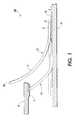
- FIG. 1is a spring contact in an undeformed free state and another spring contact deformed when contacting a contact pad;
- FIGS. 2-4show steps in a method of interconnecting two devices in accordance with the invention
- FIGS. 5-10show a plurality of types of spring contact tips
- FIG. 11shows an alternate contact structure for interconnecting two devices
- FIGS. 12 and 13show inverted “shepherd's hook” -type spring contacts
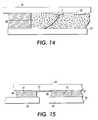
- FIG. 14shows an alternate contact structure for interconnecting two devices:
- FIG. 15shows an exemplary device interconnection structure for a liquid crystal display
- FIG. 16shows steps of a method of interconnecting two devices.
- the inventionis described below as interconnecting two different devices by applying an adhesive to at least one of the devices, aligning the contact structures of the two devices, bringing the devices into sufficient proximity (i.e., to allow the contact structures to interconnect) and curing or otherwise hardening the adhesive.
- the contact structures on the devicescan include any type of interconnect structure, such as electrical interconnect structures like contact pads and corresponding solder bumps.
- the inventionis described below in connection with using spring contacts as part of the contact structure of at least one of the interconnected devices. Accordingly, a brief description of a spring contact and how a spring contact can be made, as is fully described in U.S. Pat. Nos. 5,613,861 and 5,944,537, is provided before describing the device interconnect invention. It should be appreciated that the following description is only one example. Thus, the spring contacts can be made in any desired way, such as that described in U.S. Pat. Nos. 5,665,648 and 3,842,189, for example.
- FIG. 1shows a side view of an interconnected device structure 100 including a first device 14 that is connected to a second device 21 .
- the first device 14has a contact structure that includes a plurality of spring contacts 15 (although only one spring contact 15 is shown).
- Each spring contact 15comprises a free portion 11 and an anchor portion 12 fixed to a release layer 13 and electrically connected to a via 32 .
- Each spring contact 15is made of an extremely elastic material, such as a chrome-molybdenum alloy or a nickel-zirconium alloy.
- the spring contacts 15are formed of an elastic conductive material, although they can be formed of a non-conductive or semi-conductive material if they are coated or plated with a conductor material (assuming the devices 14 and 21 are to be electrically interconnected).
- the spring contacts 15are formed of a nickel-zirconium alloy having 1% zirconium, a chrome-molybdenum alloy (20% Cr-80% Mo), a tungsten (W)-based alloy, or a chronium (Cr) based alloy.
- Zirconiumis added to the nickel in the nickel-zirconium alloy to improve the elastic properties of the alloy while not greatly reducing the conductivity of the nickel.
- the elastic materialis not conductive, it is coated on at least one side with a conductive material, such as a metal or metal alloy.
- the via 32 and the contact pad 3 on the first and second devices 14 and 21can be the terminal ends of a communication line that electrically communicates with an electronic device formed on the first and second devices 14 and 21 , such as a transistor, a display electrode, or other electrical device, or can communicate with other contact structures such as wirebond pads, solder bumps, etc.
- the via 32 and the contact pad 3are typically made of aluminum, but can be made of any conductive material. If the contact pad 3 is made of aluminum, the contact pad 3 is preferably coated with a conductive and preferably inert material, such as gold, gold alloys, indium tin oxide, nickel, palladium, platinum, rhodium, etc.
- the spring contact 15allows the spring contact 15 to make better electrical contact with the contact pad 3 , since the spring contact 15 is not required to “scrub” the uncoated contact pad 3 to break through the aluminum oxide that forms on an uncoated aluminum contact pad 3 .
- a thin coating of Titanium (Ti)is applied to the uncoated aluminum contact pad 3 to promote good adhesion of the gold to the contact pad 3 .
- the release layer 13is made of silicon nitride or other etchable material, and can be electrically insulating or conducting. However, the release layer 13 is not necessary and can be eliminated.
- the release layer 13 and the via 32are formed on or over a first device 14 , which can have a substrate formed of an insulating material, such as oxidized silicon or glass.
- the spring contacts 15 on the device 14can be formed as follows.
- a via 32is formed on or over a substrate in the first device 14 .
- a release layer 13can be formed on or over the first device 14 .
- the release layer 13is not required and can be eliminated.
- a layer of metalis then deposited on or over a portion of the first device 14 .
- the metalis the nickel-zirconium alloy described above. Part of the metal layer is electrically connected to or directly contacts the via 32 and another portion of the metal layer is deposited on or over the release layer 13 , if present.
- the metal layeris sputter deposited.
- a plate of the metalcalled the target
- a cathodewhich is set to a high negative potential and immersed in a low-pressure, typically 1 to 100 millitorr, gas.
- a glow-discharge plasmato ignite, from which positive ions are accelerated into the negatively charged target.
- This ion bombardmentknocks metal atoms off the target, and many of these deposit on nearby surfaces, such as on the first device 14 .
- the metal layercan be thought of as deposited in several sub-layers to a final thickness of any desired thickness, e.g., approximately 1 ⁇ m.
- a stress gradientis introduced into the metal layer by altering the stress inherent in each of the sub-layers of the metal layer so that each sub-layer has a different level of inherent stress.
- Different stress levelscan be introduced into each sub-layer of the deposited metal layer during sputter deposition in a variety of ways, including adding a reactive gas to the plasma, depositing the metal at an angle, and changing the pressure of the plasma gas.
- the different levels of stressare introduced into the metal layer by varying the pressure of the plasma gas, which is preferably argon.
- the pressure of the plasma gascan be varied in a stepwise fashion, or continuously, as desired.
- the metal layeris formed so that a sub-layer near the device 14 substrate has a compressive stress and upper layers have increasingly tensile stress toward the top of the metal layer.
- the stress gradient in the metal layerbiases the layer to bend into an arc, the metal layer adheres to the release layer 13 , the first device 14 , and the contact pad 3 , and thus lies flat.
- the metal layeris photolithographically patterned into the spring contacts 15 .
- Photolithographic patterningis a well-known technique and is routinely used in the semiconductor chip industry and allows the spring contacts to be formed in almost any shape or configuration.
- the free portion 11 of the spring contact 15is released from the release layer 13 , preferably by a process of under-cut etching, i.e., removing at least a portion of the release layer 13 or other substrate under the free portion 11 .
- the spring contacts 15are released from the release layer 13 and are allowed to bend up and away from the release layer 13 due to the stress gradient in the spring contacts 15 .
- the spring contact 15contacts the pad 3 and elastically deforms. Therefore, the tip 30 of the spring contact 15 is compliantly forced into the contact pad 3 to establish an electrical contact between the contact pads 3 .
- a layer of gold or other resistance lowering materialsuch as copper, nickel, palladium, etc., can be formed over the outer surface of each spring contact 15 to reduce the resistance in the spring contacts 15 , but can be replaced with any other resistance lowering material.
- the process for forming the spring contacts 15is limited only by the design rules of photolithographic patterning, many hundreds or thousands of spring contacts 15 can be formed closely together in a relatively small area on the first device 14 .
- the typical width w of the spring contact 15can be 10-100 ⁇ m. Therefore, the spring contacts 15 can be formed close together, at a spacing of approximately 10-20 ⁇ m, and less if necessary. This makes the center-to-center die ice between adjacent spring contacts 15 approximately 20-120 ⁇ m, which is within or less than the typical center-to-center distance between adjacent contact pads 3 on a standard semiconductor chip.
- FIGS. 2-4show steps in a method for interconnecting two devices in accordance with the invention.
- a first device 14is provided that has a contact structure including at least a contact pad 3 .
- the contact structurecan of course include other interconnect structures including spring contacts, solder bumps, alignment structures that ensure alignment between interconnected devices, spacing structures that ensure proper spacing between interconnected devices, etc.
- an adhesive 40or molding compound, is applied to the first device 14 .
- the adhesive 40can be applied to portions of the first device 14 that include contact structures and/or to portions of the first device 14 that do not include contact structures.
- FIG. 2shows an example where adhesive 40 is applied over a contact structure on the first device 14 .
- the adhesive 40can be a UV-curable optically transparent adhesive, such as Loctite 352 , but other compounds, such as other UV-curable adhesives, thermal setting compounds, multi-component adhesives such as a two-part epoxy, or other compounds can be used.
- the adhesive 40or molding compound, is electrically insulating, but semiconductive, anisotropically conductive or conductive compounds could be used if desired.
- an adhesive 40that is only electrically conductive along an applied electric field, but otherwise insulating, could be used to interconnect contact pads 3 on the first and second devices 14 and 21 without requiring the contact pads 3 to physically touch.
- the adhesive 40can be applied to the first device 14 in various different ways, including using a micro-actuated applicator.
- a wireis dipped into a pool of viscous adhesive solution.
- an amount of adhesive 40is carried by the wire, and the adhesive 40 can be applied by lowering the wire to the desired portions of the first device 14 .
- the adhesive 40can also be applied to the second device 21 , if desired.
- the adhesive 40can also be applied in other ways, including spraying, injecting, etc.
- the contact structures of the first and second devices 14 and 21are next aligned with each other. That is, the contact structures, e.g., spring contacts, contact pads, etc., on the first and second devices 14 and 21 are aligned with each other so that when the first and second devices 14 and 21 are moved into sufficient proximity with each other, as shown in FIG. 4, the contact structures interconnect the devices 14 and 21 .
- the interconnectioncan be electrical interconnection and/or physical interconnection.
- the process of bringing the first and second devices 14 and 21 into sufficient proximitycan involve steps other than simply moving the devices 14 and 21 together.
- the first and second devices 14 and 21 and or elements in the respective contact structurescan be moved laterally relative to each other to scrub the spring contacts 15 into the corresponding contact pads 3 .
- excess adhesive 40is squeezed out and a thin layer of adhesive 40 is trapped between the devices 14 and 21 to encapsulate the entire package.
- the adhesive 40is cured or otherwise hardened to bond the devices 14 and 21 as well as their contact structures together.
- the devicescan be or include any type of apparatus such as a circuit board or other electrical interconnection device, a laser emitting element, a light modulating element, a light detecting element, a vertical cavity surface emitting laser, a light emitting diode, an edge emitting laser, a switching element, a controller, a data processing apparatus, a semiconductor chip, a semiconductor memory or logic chip, an optoelectronics module, and a micro-electro-mechanical device
- the inventorshave discovered that when at least one of the devices 14 and 21 includes spring contacts 15 as part of its contact structure, the devices 14 and 21 should be interconnected by first applying adhesive to at least one of the devices 14 and 21 and then assembling the devices 14 and 21 into a final package, especially when the spring contacts 15 are very thin, e.g., 5-20 microns. That is, the inventors have found that the interconnection between contact structures of the devices 14 and 21 can be disrupted if the adhesive 40 is injected between the devices in a conventional fashion after the contact structures are interconnected, e.g., injecting adhesive 40 after somewhat delicate spring contacts 15 and corresponding contact pads 3 are electrically connected.
- the electrical interconnect between the spring contacts 15 and the contact pads 3is disrupted by the surface tension of the adhesive 40 as it flows between the devices 14 and 21 , and some of the adhesive 40 forces itself between the spring contacts 15 and their corresponding contact pads 3 . Accordingly, applying the adhesive 40 to at least one of the devices 14 and 21 before the devices 14 and 21 are moved together and the contact structures interconnected can be critical to proper assembly of two devices having spring contacts 15 as part of a contact structure.
- Applying the adhesive 40 to one of the devices 14 and 21 before assemblyalso has the benefit of reducing the likelihood of void formation in the adhesive 40 since pressure is applied to the adhesive 40 when the devices 14 and 21 are moved together and the adhesive 40 is squeezed out from between the devices 14 and 21 .
- Interconnecting the devices 14 and 21 according to the inventionalso has the benefit of shorter assembly time since adhesive 40 can be forced out from between the devices 14 and 21 more quickly than adhesive 40 can be injected or wicked into the space between devices 14 and 21 after the devices 14 and 21 have been brought together.
- the adhesive 40can also provide a sealing function against atmospheric contaminants and, if properly selected, the adhesive 40 does not contribute contaminants of its own.
- the adhesive 40can undergo a slight contraction, e.g., up to 4%, which increases the compressive force of the spring contact 15 into the contact pad 3 .
- This compressionis caused by shrinkage of the adhesive 40 in the y direction, as shown in FIG. 4 .
- the adhesive 40shrinks in the y direction rather than the x direction because when the adhesive 40 is bonded to the first device 14 and the second device 21 , the first device 14 and the second device 21 resist shrinkage of the adhesive 40 in the x direction.
- the additional compressive force provided between the spring contact 15 and the contact pad 3will remain over a relatively wide temperature range, providing of course that the differential thermal expansion of the adhesive 40 relative to the contacts does not exceed the initial contraction value of, for example, 4%.
- the adhesive 40can also perform a heat sink function to remove heat from elements of the devices 14 and 21 .
- FIGS. 5-10show various tip 30 configurations for spring contacts 15 used with the invention.
- the shape of the spring contact tip 30can take different forms, depending on the application. Since the spring contacts 15 are photolithographically patterned, the spring contact tips 30 are easily formed in a variety of shapes.
- FIG. 5shows a spring contact tip 30 having a flat end.
- the spring contact tip 30 shown in FIG. 6has a pointed end which concentrates the force exerted by the spring contact 15 at a single point on the contact pad 3 . This pointed shape aids the spring contact tip 30 when breaking through native oxides which may be present on the contact pads 3 .
- FIGS. 7 and 8show spring contact tips 30 having multiple points for applications where contact redundancy is required.
- FIG. 9shows a spring contact tip 30 having a deformable tab.
- the deformable tabincreases the contact area with the contact pad 3 by deforming as shown in FIG. 10 when the spring contact 15 forces the tip 30 against the contact pad 3 .
- a tip 30 having a flat or deformable endhas been found to reduce resistance at the point of contact.
- FIG. 11shows an alternate type of spring contact that can be used with the invention.
- the spring contact 15is formed so that when it is released from the surface of the first device 14 , the free end of the spring contact 15 curls back to form an arc of 180 degrees or more.
- This arrangementcan be advantageous when a large contact area is needed between the spring contact 15 and the contact pad 3 , or when relative movement between the second device 21 and the first device 14 in the x direction might stress the spring contact 15 /contact pad 3 joint. Relative movement in the x direction is compensated for by flexure in the curved portion of the spring contact 15 between the contact pad 3 and the first device 14 .
- spring contact 15 configurationsinclude that shown in FIGS. 12 and 13.
- the bottom-most portion of the spring contacts 15have a tensile stress, while upper portions have decreasing levels of tensile stress and/or increasing levels of compressive stress. Therefore, when the free portion 11 of the spring contact 15 is released from the first device 14 , the free portion 11 bends so that the spring contact 15 moves up and away from the first device 14 .
- These configurationshave an advantage over other configurations where the free portion 11 does not contact the first device 14 after the free portion 11 is released, e.g., FIG. 1, in that the free portion 11 tends not to move too freely in the z direction shown in FIGS. 12 and 13. This can be an advantage in fine-pitch contact applications where the spring contacts 15 are spaced closely together, e.g., less than 10 ⁇ m apart, and can become entangled with each other.
- FIG. 14shows another configuration of two interconnected devices 14 and 21 where the contact structures, or one of the contact structures, of the devices 14 and 21 include an aligning or spacing structure 36 .
- the structure 36can, for example, have aligning grooves or bumps that interlock when the devices 14 and 21 are moved together, thus ensuring that the contact structures of the devices 14 and 21 are properly aligned.
- the structure 36can also ensure that the devices 14 and 21 are properly spaced apart, e.g., when the device 14 is an LCD panel backplane and the device 21 is an LCD panel front plane.
- the structure 36can also function to contain the adhesive 40 and/or prevent the adhesive 40 from contacting certain portions of the contacting structures, e.g., particularly sensitive or fine structures.
- the first and second devices 14 and 21can include any type of elements, such as switching elements (transistors), data processing elements, light emitting elements, etc.
- the element 35can be an LED or laser emitter and can communicate through the spring contact 15 to a driver on the first device 14 that controls the element 35 to selectively emit light.
- the adhesive 40 and the substrate of the first device 14can be transparent so that the element 35 can emit light through the adhesive 40 and the device 14 substrate while being protected from a harmful environment.
- the devices 14 and 21can be any desired set of devices that are interconnected, including, a circuit board, a semiconductor chip, a probe card, or other electronic devices.
- FIG. 15shows one detailed example of how three devices in a liquid crystal display (LCD) can be interconnected using the invention.
- an active matrix backplane 22 for the LCD and an off-display board 24such as a device driver, are interconnected with an LCD front plane 23 .
- the contact structure of the active matrix backplane 22 and the off-display board 24can include contact pads 3 , spring contacts 15 , metal traces, wirebond pads, bumps, tabs, etc.
- the contact structure of the LCD front plane 23can include metal traces (including indium-tin oxide (ITO) traces), spring contacts 15 , contact pads 3 , wirebond pads, bumps, tabs, etc.
- ITOindium-tin oxide
- the front plane 23includes spring contacts 15 that connect with contact pads 3 , traces or other structures (not shown) on the active matrix backplane 22 and the off-display board 24 .
- a conductive trace 51 or other structureelectrically connects the two spring contacts 15 shown so that appropriate elements in the active matrix backplane 22 and the off-display board 24 can communicate.
- adhesive 40is applied to the active matrix backplane 22 , the LCD front plane and/or the off-display board 24 .
- the backplane 22 , the front plane 23 and the off-display board 24are aligned and moved into sufficient proximity so that the respective contact structures interconnect.
- the adhesive 40is then cured or otherwise hardened to bond the devices 22 , 23 and 24 together.
- a liquid crystal material 52can be provided between the backplane 22 and the front plane 23 in a conventional fashion.
- the adhesive 40typically an epoxy, can function to both bond the devices 22 , 23 and 24 together in accordance with the invention as well as provide a sealing function for the liquid crystal material 52 .
- the spring contacts 15can also be arranged so that the spring contact tips 30 extend from the adhesive 40 into the liquid crystal material 52 to contact a structure on the backplane 22 .
- the devices 22 , 23 and 24are described as a backplane, front plane and off-display board, the devices 22 , 23 and 24 could be replaced with other devices such as a laser emitting or laser array device for the device 22 , an electronic device, such as an array of transistors and/or other switching elements for the device 23 and a photodetector or array of photodetectors for the device 24 . Such an arrangement could be used, for example, as a scanning device.
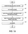
- FIG. 16shows steps of a method for interconnecting two devices.
- a first deviceis provided having a contact structure.
- the first devicecan include a single device or a group of devices that perform any desired function, such as a display driver, data processor, display, electrical interconnect, heat sink, light or other radiation emitter, detector or modulator, data storage, interface, etc.
- the contact structure associated with the first devicecan include any desired physical or electrical interconnect structure, such as contact pads, spring contacts, metal traces, wirebond pads, bumps, tabs, spacers, alignment features, etc.
- the contact structureincludes spring contacts for electrical interconnection with a corresponding contact pad.
- an adhesiveis applied to either the first or second device.
- the adhesivecan be applied to the contact structure or portions of the contact structure of either of the devices and/or to portions of the device that include no contact structure.
- the adhesivecan be any kind of compound having various different mechanical and/or electrical properties.
- the adhesivecan be a UV-curable optically transparent adhesive, such as Loctite 352 , but other compounds, such as other UV-curable adhesives, thermal setting compounds, multi-component adhesives such as two-part epoxy or other compounds can be used.
- the adhesiveis electrically insulating, but semiconductive, anisotropically conductive or conductive compounds could be used if desired.
- an adhesive that is only electrically conductive along an applied electric field, but otherwise insulatingcould be used to interconnect contact pads on the first and second devices without requiring the contact pads to physically touch.
- the adhesivecan be applied to the devices in various different ways, including using a micro-actuated applicator.
- a micro-actuated applicatorWhen using a micro-actuated applicator, a wire is dipped into a pool of viscous adhesive solution. When the wire is lifted from the pool, an amount of adhesive is carried by the wire, and the adhesive can be applied by lowering the wire to the desired portions of the first device.
- step S 30the second device having a complementary contact structure to the first device is aligned with the first device.
- the second devicecan be a single device or a group of devices that perform any desired function.
- the second devicecan also have a contact structure including any of the elements mentioned above.
- step S 40the first and second devices are brought into sufficient proximity to each other, preferably so that the contact structures interconnect either physically and/or electrically. Bringing the devices into sufficient proximity also can cause adhesive to flow in the space between the devices and preferably allows the adhesive to surround at least some of the contact structures of the first and second devices. This adhesive flow can prevent voids from forming in the adhesive and ensure the contact structures on the devices are surrounded by adhesive.
- step S 50the adhesive is cured or otherwise hardened, e.g., by exposing the adhesive to UV radiation, Of course, other methods for hardening or setting the adhesive can be used depending on the type of adhesive.
Landscapes
- Engineering & Computer Science (AREA)
- Microelectronics & Electronic Packaging (AREA)
- Computer Hardware Design (AREA)
- Power Engineering (AREA)
- Manufacturing & Machinery (AREA)
- General Physics & Mathematics (AREA)
- Condensed Matter Physics & Semiconductors (AREA)
- Physics & Mathematics (AREA)
- Metallurgy (AREA)
- Measuring Leads Or Probes (AREA)
- Connections Effected By Soldering, Adhesion, Or Permanent Deformation (AREA)
- Electric Connection Of Electric Components To Printed Circuits (AREA)
- Encapsulation Of And Coatings For Semiconductor Or Solid State Devices (AREA)
- Wire Bonding (AREA)
Abstract
Description
Claims (32)
Priority Applications (1)
| Application Number | Priority Date | Filing Date | Title |
|---|---|---|---|
| US09/794,101US6439898B2 (en) | 1999-12-15 | 2001-02-28 | Method and apparatus for interconnecting devices using an adhesive |
Applications Claiming Priority (2)
| Application Number | Priority Date | Filing Date | Title |
|---|---|---|---|
| US09/461,195US6213789B1 (en) | 1999-12-15 | 1999-12-15 | Method and apparatus for interconnecting devices using an adhesive |
| US09/794,101US6439898B2 (en) | 1999-12-15 | 2001-02-28 | Method and apparatus for interconnecting devices using an adhesive |
Related Parent Applications (1)
| Application Number | Title | Priority Date | Filing Date |
|---|---|---|---|
| US09/461,195ContinuationUS6213789B1 (en) | 1999-12-15 | 1999-12-15 | Method and apparatus for interconnecting devices using an adhesive |
Publications (2)
| Publication Number | Publication Date |
|---|---|
| US20010053620A1 US20010053620A1 (en) | 2001-12-20 |
| US6439898B2true US6439898B2 (en) | 2002-08-27 |
Family
ID=23831581
Family Applications (2)
| Application Number | Title | Priority Date | Filing Date |
|---|---|---|---|
| US09/461,195Expired - LifetimeUS6213789B1 (en) | 1999-12-15 | 1999-12-15 | Method and apparatus for interconnecting devices using an adhesive |
| US09/794,101Expired - LifetimeUS6439898B2 (en) | 1999-12-15 | 2001-02-28 | Method and apparatus for interconnecting devices using an adhesive |
Family Applications Before (1)
| Application Number | Title | Priority Date | Filing Date |
|---|---|---|---|
| US09/461,195Expired - LifetimeUS6213789B1 (en) | 1999-12-15 | 1999-12-15 | Method and apparatus for interconnecting devices using an adhesive |
Country Status (2)
| Country | Link |
|---|---|
| US (2) | US6213789B1 (en) |
| JP (1) | JP4516205B2 (en) |
Cited By (23)
| Publication number | Priority date | Publication date | Assignee | Title |
|---|---|---|---|---|
| US20020153092A1 (en)* | 2000-11-10 | 2002-10-24 | Rinne Glenn A. | Methods of positioning components using liquid prime movers and related structures |
| US20030184217A1 (en)* | 2002-03-26 | 2003-10-02 | Semiconductor Energy Laboratory Co., Ltd. | Light emitting device and method of manufacturing the same |
| US20040166702A1 (en)* | 2003-02-25 | 2004-08-26 | Shinko Electric Industries Co., Ltd. | Semiconductor device having external contact terminals and method for using the same |
| US6815961B2 (en) | 1999-07-28 | 2004-11-09 | Nanonexus, Inc. | Construction structures and manufacturing processes for integrated circuit wafer probe card assemblies |
| US6844214B1 (en) | 2003-08-21 | 2005-01-18 | Xerox, Corporation | Microelectromechanical system based sensors, sensor arrays, sensing systems, sensing methods and methods of fabrication |
| US20050026476A1 (en)* | 2000-06-20 | 2005-02-03 | Sammy Mok | Systems for testing and packaging integrated circuits |
| US20050130462A1 (en)* | 2003-12-15 | 2005-06-16 | Palo Alto Research Center, Incorporated | Stressed metal contact with enhanced lateral compliance |
| US7009412B2 (en) | 1999-05-27 | 2006-03-07 | Nanonexus, Inc. | Massively parallel interface for electronic circuit |
| US20060055055A1 (en)* | 2004-09-13 | 2006-03-16 | Infineon Technologies Ag | Semiconductor chip with flexible contacts at a face |
| US20060116010A1 (en)* | 2004-11-29 | 2006-06-01 | Palo Alto Research Center Incorporated | Latching structure and a method of making an electrical interconnect |
| US20060131163A1 (en)* | 2004-12-16 | 2006-06-22 | Xerox Corporation | Variable volume between flexible structure and support surface |
| US20060210237A1 (en)* | 2005-03-18 | 2006-09-21 | Kaoru Soeta | Electronic function part mounted body and method of manufacturing the electronic function part mounted body |
| US20070125486A1 (en)* | 2005-12-02 | 2007-06-07 | Palo Alto Research Center Incorporated | Vertically spaced plural microsprings |
| US7349223B2 (en) | 2000-05-23 | 2008-03-25 | Nanonexus, Inc. | Enhanced compliant probe card systems having improved planarity |
| US7382142B2 (en) | 2000-05-23 | 2008-06-03 | Nanonexus, Inc. | High density interconnect system having rapid fabrication cycle |
| US20080188107A1 (en)* | 2007-02-01 | 2008-08-07 | Motorola, Inc. | Submersible electrical connector assembly and method of forming same |
| US20090159996A1 (en)* | 2007-12-21 | 2009-06-25 | Palo Alto Research Center Incorporated | Method Of Producing Microsprings Having Nanowire Tip Structures |
| US7579848B2 (en) | 2000-05-23 | 2009-08-25 | Nanonexus, Inc. | High density interconnect system for IC packages and interconnect assemblies |
| US7952373B2 (en) | 2000-05-23 | 2011-05-31 | Verigy (Singapore) Pte. Ltd. | Construction structures and manufacturing processes for integrated circuit wafer probe card assemblies |
| US8441808B2 (en) | 2010-09-22 | 2013-05-14 | Palo Alto Research Center Incorporated | Interposer with microspring contacts |
| US8519534B2 (en) | 2010-09-22 | 2013-08-27 | Palo Alto Research Center Incorporated | Microsprings partially embedded in a laminate structure and methods for producing same |
| US8525353B2 (en) | 2011-12-19 | 2013-09-03 | Palo Alto Research Center Incorporated | Microspring structures adapted for target device cooling |
| US11054593B1 (en)* | 2020-03-11 | 2021-07-06 | Palo Alto Research Center Incorporated | Chip-scale optoelectronic transceiver with microspringed interposer |
Families Citing this family (31)
| Publication number | Priority date | Publication date | Assignee | Title |
|---|---|---|---|---|
| US6710609B2 (en)* | 2002-07-15 | 2004-03-23 | Nanonexus, Inc. | Mosaic decal probe |
| US20070245553A1 (en)* | 1999-05-27 | 2007-10-25 | Chong Fu C | Fine pitch microfabricated spring contact structure & method |
| US20050068054A1 (en)* | 2000-05-23 | 2005-03-31 | Sammy Mok | Standardized layout patterns and routing structures for integrated circuit wafer probe card assemblies |
| US6505811B1 (en)* | 2000-06-27 | 2003-01-14 | Kelsey-Hayes Company | High-pressure fluid control valve assembly having a microvalve device attached to fluid distributing substrate |
| US6528350B2 (en) | 2001-05-21 | 2003-03-04 | Xerox Corporation | Method for fabricating a metal plated spring structure |
| US6747298B2 (en) | 2001-07-23 | 2004-06-08 | Cree, Inc. | Collets for bonding of light emitting diodes having shaped substrates |
| US6888167B2 (en)* | 2001-07-23 | 2005-05-03 | Cree, Inc. | Flip-chip bonding of light emitting devices and light emitting devices suitable for flip-chip bonding |
| WO2003018865A1 (en)* | 2001-08-24 | 2003-03-06 | Nanonexus, Inc. | Method and apparatus for producing uniform isotropic stresses in a sputtered film |
| US6866255B2 (en)* | 2002-04-12 | 2005-03-15 | Xerox Corporation | Sputtered spring films with low stress anisotropy |
| US7006720B2 (en)* | 2002-04-30 | 2006-02-28 | Xerox Corporation | Optical switching system |
| US6891240B2 (en) | 2002-04-30 | 2005-05-10 | Xerox Corporation | Electrode design and positioning for controlled movement of a moveable electrode and associated support structure |
| US7241420B2 (en)* | 2002-08-05 | 2007-07-10 | Palo Alto Research Center Incorporated | Capillary-channel probes for liquid pickup, transportation and dispense using stressy metal |
| US8080221B2 (en)* | 2002-08-05 | 2011-12-20 | Palo Alto Research Center Incorporated | Capillary-channel probes for liquid pickup, transportation and dispense using stressy metal |
| TW590982B (en)* | 2002-09-27 | 2004-06-11 | Agnitio Science & Technology I | Micro-fluid driving device |
| US7015584B2 (en)* | 2003-07-08 | 2006-03-21 | Xerox Corporation | High force metal plated spring structure |
| US7410590B2 (en)* | 2003-12-19 | 2008-08-12 | Palo Alto Research Center Incorporated | Transferable micro spring structure |
| US7082684B2 (en)* | 2004-08-04 | 2006-08-01 | Palo Alto Research Center Incorporated | Intermetallic spring structure |
| US20060030179A1 (en)* | 2004-08-05 | 2006-02-09 | Palo Alto Research Center, Incorporated | Transmission-line spring structure |
| US8330485B2 (en)* | 2004-10-21 | 2012-12-11 | Palo Alto Research Center Incorporated | Curved spring structure with downturned tip |
| US7230440B2 (en) | 2004-10-21 | 2007-06-12 | Palo Alto Research Center Incorporated | Curved spring structure with elongated section located under cantilevered section |
| US7292294B2 (en)* | 2004-11-03 | 2007-11-06 | Chunghwa Picture Tubes, Ltd. | Manufacturing method of color filter on TFT array and manufacturing method of LCD panel |
| TWI401488B (en) | 2004-11-23 | 2013-07-11 | Samsung Display Co Ltd | Display device |
| JP5053542B2 (en)* | 2005-11-25 | 2012-10-17 | 東京エレクトロン株式会社 | Probe pin and method of manufacturing probe pin |
| US7982290B2 (en)* | 2006-01-12 | 2011-07-19 | Palo Alto Research Center, Inc. | Contact spring application to semiconductor devices |
| TWI351670B (en)* | 2006-05-18 | 2011-11-01 | Au Optronics Corp | Signal transmission assembly and display panel app |
| EP2197782B1 (en)* | 2007-09-12 | 2020-03-04 | Smoltek AB | Connecting and bonding adjacent layers with nanostructures |
| JP5239926B2 (en)* | 2009-02-16 | 2013-07-17 | 株式会社デンソー | Electronic device and manufacturing method thereof |
| US8405198B2 (en) | 2009-05-22 | 2013-03-26 | Palo Alto Research Center Incorporated | Stress-engineered interconnect packages with activator-assisted molds |
| US8039938B2 (en)* | 2009-05-22 | 2011-10-18 | Palo Alto Research Center Incorporated | Airgap micro-spring interconnect with bonded underfill seal |
| JP5884378B2 (en)* | 2011-09-30 | 2016-03-15 | ブラザー工業株式会社 | Display device and image forming apparatus |
| WO2013061486A1 (en)* | 2011-10-26 | 2013-05-02 | ユニテクノ株式会社 | Contact probe and inspection socket provided with same |
Citations (25)
| Publication number | Priority date | Publication date | Assignee | Title |
|---|---|---|---|---|
| US2562685A (en) | 1949-06-04 | 1951-07-31 | Soren S Adams | Thermostatic snap-action element |
| US3356369A (en) | 1965-01-22 | 1967-12-05 | Kolmer Bros Inc | Die agitating chance device |
| US3826984A (en) | 1969-02-28 | 1974-07-30 | Licentia Gmbh | Measuring device for the dynamic measurement of semiconductor parameters and method of making such a device |
| US3842189A (en)* | 1973-01-08 | 1974-10-15 | Rca Corp | Contact array and method of making the same |
| US4320438A (en) | 1980-05-15 | 1982-03-16 | Cts Corporation | Multi-layer ceramic package |
| US4423401A (en) | 1982-07-21 | 1983-12-27 | Tektronix, Inc. | Thin-film electrothermal device |
| US4758927A (en) | 1987-01-21 | 1988-07-19 | Tektronix, Inc. | Method of mounting a substrate structure to a circuit board |
| US5032006A (en) | 1988-09-16 | 1991-07-16 | Asulab, S.A. | Electrooptical cells having connection means |
| US5090118A (en) | 1990-07-31 | 1992-02-25 | Texas Instruments Incorporated | High performance test head and method of making |
| US5121298A (en) | 1988-08-16 | 1992-06-09 | Delco Electronics Corporation | Controlled adhesion conductor |
| US5142644A (en) | 1991-03-08 | 1992-08-25 | General Motors Corporation | Electrical contacts for polymer dispersed liquid crystal films |
| US5152695A (en) | 1991-10-10 | 1992-10-06 | Amp Incorporated | Surface mount electrical connector |
| US5233451A (en) | 1990-12-27 | 1993-08-03 | Seiko Epson Corporation | Liquid crystal display device with chamfered substrate edge |
| US5280139A (en) | 1990-03-01 | 1994-01-18 | Motorola, Inc. | Selectively releasing conductive runner and substrate assembly |
| WO1994009374A1 (en) | 1992-10-12 | 1994-04-28 | Kabushiki Kaisha Kobe Seiko Sho | Probe unit and method of manufacturing the same |
| JPH06249880A (en) | 1993-03-01 | 1994-09-09 | Kobe Steel Ltd | Probe unit |
| US5487999A (en) | 1991-06-04 | 1996-01-30 | Micron Technology, Inc. | Method for fabricating a penetration limited contact having a rough textured surface |
| US5513430A (en) | 1994-08-19 | 1996-05-07 | Motorola, Inc. | Method for manufacturing a probe |
| WO1996041506A1 (en) | 1995-06-07 | 1996-12-19 | Xerox Corporation | Photolithographically patterned spring contact |
| US5665648A (en)* | 1995-12-21 | 1997-09-09 | Hughes Electronics | Integrated circuit spring contact fabrication methods |
| US5789766A (en)* | 1997-03-20 | 1998-08-04 | Motorola, Inc. | Led array with stacked driver circuits and methods of manfacture |
| WO1999018445A1 (en) | 1997-10-02 | 1999-04-15 | New Jersey Institute Of Technology | Micromachined element and method of fabrication thereof |
| US5944537A (en)* | 1997-12-15 | 1999-08-31 | Xerox Corporation | Photolithographically patterned spring contact and apparatus and methods for electrically contacting devices |
| US6031590A (en) | 1997-01-22 | 2000-02-29 | Lg Electronics Inc. | Structure and method of mounting driver IC using anisotropic conductive film in liquid crystal display device |
| US6288417B1 (en)* | 1999-01-07 | 2001-09-11 | Xerox Corporation | Light-emitting devices including polycrystalline gan layers and method of forming devices |
Family Cites Families (2)
| Publication number | Priority date | Publication date | Assignee | Title |
|---|---|---|---|---|
| JPH0674972A (en)* | 1992-08-27 | 1994-03-18 | Shinko Electric Ind Co Ltd | Contact probe |
| JPH11345834A (en)* | 1998-06-01 | 1999-12-14 | Matsushita Electric Ind Co Ltd | Semiconductor element, method of manufacturing semiconductor device using the same, and semiconductor device |
- 1999
- 1999-12-15USUS09/461,195patent/US6213789B1/ennot_activeExpired - Lifetime
- 2000
- 2000-12-07JPJP2000372324Apatent/JP4516205B2/ennot_activeExpired - Fee Related
- 2001
- 2001-02-28USUS09/794,101patent/US6439898B2/ennot_activeExpired - Lifetime
Patent Citations (26)
| Publication number | Priority date | Publication date | Assignee | Title |
|---|---|---|---|---|
| US2562685A (en) | 1949-06-04 | 1951-07-31 | Soren S Adams | Thermostatic snap-action element |
| US3356369A (en) | 1965-01-22 | 1967-12-05 | Kolmer Bros Inc | Die agitating chance device |
| US3826984A (en) | 1969-02-28 | 1974-07-30 | Licentia Gmbh | Measuring device for the dynamic measurement of semiconductor parameters and method of making such a device |
| US3842189A (en)* | 1973-01-08 | 1974-10-15 | Rca Corp | Contact array and method of making the same |
| US4320438A (en) | 1980-05-15 | 1982-03-16 | Cts Corporation | Multi-layer ceramic package |
| US4423401A (en) | 1982-07-21 | 1983-12-27 | Tektronix, Inc. | Thin-film electrothermal device |
| US4758927A (en) | 1987-01-21 | 1988-07-19 | Tektronix, Inc. | Method of mounting a substrate structure to a circuit board |
| US5121298A (en) | 1988-08-16 | 1992-06-09 | Delco Electronics Corporation | Controlled adhesion conductor |
| US5032006A (en) | 1988-09-16 | 1991-07-16 | Asulab, S.A. | Electrooptical cells having connection means |
| US5280139A (en) | 1990-03-01 | 1994-01-18 | Motorola, Inc. | Selectively releasing conductive runner and substrate assembly |
| US5090118A (en) | 1990-07-31 | 1992-02-25 | Texas Instruments Incorporated | High performance test head and method of making |
| US5233451A (en) | 1990-12-27 | 1993-08-03 | Seiko Epson Corporation | Liquid crystal display device with chamfered substrate edge |
| US5142644A (en) | 1991-03-08 | 1992-08-25 | General Motors Corporation | Electrical contacts for polymer dispersed liquid crystal films |
| US5487999A (en) | 1991-06-04 | 1996-01-30 | Micron Technology, Inc. | Method for fabricating a penetration limited contact having a rough textured surface |
| US5152695A (en) | 1991-10-10 | 1992-10-06 | Amp Incorporated | Surface mount electrical connector |
| WO1994009374A1 (en) | 1992-10-12 | 1994-04-28 | Kabushiki Kaisha Kobe Seiko Sho | Probe unit and method of manufacturing the same |
| JPH06249880A (en) | 1993-03-01 | 1994-09-09 | Kobe Steel Ltd | Probe unit |
| US5513430A (en) | 1994-08-19 | 1996-05-07 | Motorola, Inc. | Method for manufacturing a probe |
| WO1996041506A1 (en) | 1995-06-07 | 1996-12-19 | Xerox Corporation | Photolithographically patterned spring contact |
| US5613861A (en)* | 1995-06-07 | 1997-03-25 | Xerox Corporation | Photolithographically patterned spring contact |
| US5665648A (en)* | 1995-12-21 | 1997-09-09 | Hughes Electronics | Integrated circuit spring contact fabrication methods |
| US6031590A (en) | 1997-01-22 | 2000-02-29 | Lg Electronics Inc. | Structure and method of mounting driver IC using anisotropic conductive film in liquid crystal display device |
| US5789766A (en)* | 1997-03-20 | 1998-08-04 | Motorola, Inc. | Led array with stacked driver circuits and methods of manfacture |
| WO1999018445A1 (en) | 1997-10-02 | 1999-04-15 | New Jersey Institute Of Technology | Micromachined element and method of fabrication thereof |
| US5944537A (en)* | 1997-12-15 | 1999-08-31 | Xerox Corporation | Photolithographically patterned spring contact and apparatus and methods for electrically contacting devices |
| US6288417B1 (en)* | 1999-01-07 | 2001-09-11 | Xerox Corporation | Light-emitting devices including polycrystalline gan layers and method of forming devices |
Non-Patent Citations (7)
| Title |
|---|
| A. Lee, J. Hamilton, J. Trevino, "A Low Power, Tight Seal, Polyimide Electrostatic Microvalve," Mirco-Electro-Mechanical Systems ASME, Dynamic Systems and Control Division Publication, v. 56, pp. 345-349, Nov. 17, 1996. |
| A.E. "Bill" Corwith, "Probing at Die Level", Advanced Packaging, Jan./Feb. 1995, p. 26 & 28. |
| Donald L. Smith et al., "A New Flip-Chip Technology for High-Density Packaging," Proc. 46th Electronic Components and Technology Conf., May 1996. |
| Donald L. Smith et al., "A New, High-Compliance Flip-Chip Technology," Display Works Conference, Feb. 1996. |
| Donald L. Smith et al., "Flip-Chip Bonding On 6-Um Pitch Thin-Film Microspring Technology," to be published in Proc. 48th Electronic Components And Technology Conf., May 1998. |
| IBM Technical Disclosure vol. 34, No. 78, Dec. 1991. |
| K. Bohringer, "Computational Methods for Design and Control of MEMS Actuator Arrays," Sep. 12, 1997, Abstract from Seminar. |
Cited By (46)
| Publication number | Priority date | Publication date | Assignee | Title |
|---|---|---|---|---|
| US7009412B2 (en) | 1999-05-27 | 2006-03-07 | Nanonexus, Inc. | Massively parallel interface for electronic circuit |
| US7772860B2 (en) | 1999-05-27 | 2010-08-10 | Nanonexus, Inc. | Massively parallel interface for electronic circuit |
| US7403029B2 (en) | 1999-05-27 | 2008-07-22 | Nanonexus Corporation | Massively parallel interface for electronic circuit |
| US7884634B2 (en) | 1999-05-27 | 2011-02-08 | Verigy (Singapore) Pte, Ltd | High density interconnect system having rapid fabrication cycle |
| US6815961B2 (en) | 1999-07-28 | 2004-11-09 | Nanonexus, Inc. | Construction structures and manufacturing processes for integrated circuit wafer probe card assemblies |
| US7952373B2 (en) | 2000-05-23 | 2011-05-31 | Verigy (Singapore) Pte. Ltd. | Construction structures and manufacturing processes for integrated circuit wafer probe card assemblies |
| US7349223B2 (en) | 2000-05-23 | 2008-03-25 | Nanonexus, Inc. | Enhanced compliant probe card systems having improved planarity |
| US7382142B2 (en) | 2000-05-23 | 2008-06-03 | Nanonexus, Inc. | High density interconnect system having rapid fabrication cycle |
| US7872482B2 (en) | 2000-05-23 | 2011-01-18 | Verigy (Singapore) Pte. Ltd | High density interconnect system having rapid fabrication cycle |
| US7579848B2 (en) | 2000-05-23 | 2009-08-25 | Nanonexus, Inc. | High density interconnect system for IC packages and interconnect assemblies |
| US20050026476A1 (en)* | 2000-06-20 | 2005-02-03 | Sammy Mok | Systems for testing and packaging integrated circuits |
| US7621761B2 (en) | 2000-06-20 | 2009-11-24 | Nanonexus, Inc. | Systems for testing and packaging integrated circuits |
| US20060240690A9 (en)* | 2000-06-20 | 2006-10-26 | Sammy Mok | Systems for testing and packaging integrated circuits |
| US7247035B2 (en) | 2000-06-20 | 2007-07-24 | Nanonexus, Inc. | Enhanced stress metal spring contactor |
| US20020153092A1 (en)* | 2000-11-10 | 2002-10-24 | Rinne Glenn A. | Methods of positioning components using liquid prime movers and related structures |
| US7213740B2 (en) | 2000-11-10 | 2007-05-08 | Unitive International Limited | Optical structures including liquid bumps and related methods |
| US7032806B2 (en)* | 2000-11-10 | 2006-04-25 | Unitive Electronics, Inc. | Methods of positioning components using liquid prime movers and related structures |
| US7629018B2 (en) | 2002-03-26 | 2009-12-08 | Semiconductor Energy Laboratory Co., Ltd. | Light emitting device and method of manufacturing the same |
| US7190335B2 (en)* | 2002-03-26 | 2007-03-13 | Semiconductor Energy Laboratory Co., Ltd. | Light emitting device and method of manufacturing the same |
| US20070160746A1 (en)* | 2002-03-26 | 2007-07-12 | Shunpei Yamazaki | Light emitting device and method of manufacturing the same |
| US20030184217A1 (en)* | 2002-03-26 | 2003-10-02 | Semiconductor Energy Laboratory Co., Ltd. | Light emitting device and method of manufacturing the same |
| US7025600B2 (en)* | 2003-02-25 | 2006-04-11 | Shinko Electric Industries Co., Ltd. | Semiconductor device having external contact terminals and method for using the same |
| US20040166702A1 (en)* | 2003-02-25 | 2004-08-26 | Shinko Electric Industries Co., Ltd. | Semiconductor device having external contact terminals and method for using the same |
| US6844214B1 (en) | 2003-08-21 | 2005-01-18 | Xerox, Corporation | Microelectromechanical system based sensors, sensor arrays, sensing systems, sensing methods and methods of fabrication |
| US7160121B2 (en)* | 2003-12-15 | 2007-01-09 | Palo Alto Research Center Incorporated | Stressed metal contact with enhanced lateral compliance |
| US20050130462A1 (en)* | 2003-12-15 | 2005-06-16 | Palo Alto Research Center, Incorporated | Stressed metal contact with enhanced lateral compliance |
| US7375434B2 (en)* | 2004-09-13 | 2008-05-20 | Infineon Technologies Ag | Semiconductor chip with flexible contacts at a face |
| US20060055055A1 (en)* | 2004-09-13 | 2006-03-16 | Infineon Technologies Ag | Semiconductor chip with flexible contacts at a face |
| US20060116010A1 (en)* | 2004-11-29 | 2006-06-01 | Palo Alto Research Center Incorporated | Latching structure and a method of making an electrical interconnect |
| US7710371B2 (en) | 2004-12-16 | 2010-05-04 | Xerox Corporation | Variable volume between flexible structure and support surface |
| US20060131163A1 (en)* | 2004-12-16 | 2006-06-22 | Xerox Corporation | Variable volume between flexible structure and support surface |
| US20060210237A1 (en)* | 2005-03-18 | 2006-09-21 | Kaoru Soeta | Electronic function part mounted body and method of manufacturing the electronic function part mounted body |
| US20070125486A1 (en)* | 2005-12-02 | 2007-06-07 | Palo Alto Research Center Incorporated | Vertically spaced plural microsprings |
| US7550855B2 (en) | 2005-12-02 | 2009-06-23 | Palo Alto Research Center Incorporated | Vertically spaced plural microsprings |
| US20080188107A1 (en)* | 2007-02-01 | 2008-08-07 | Motorola, Inc. | Submersible electrical connector assembly and method of forming same |
| US7484981B2 (en)* | 2007-02-01 | 2009-02-03 | Motorola, Inc. | Assembly for sealing an audio connector within an electronic device |
| US20110167526A1 (en)* | 2007-12-21 | 2011-07-07 | Palo Alto Research Center Incorporated | Microsprings Having Nanowire Tip Structures |
| US20090159996A1 (en)* | 2007-12-21 | 2009-06-25 | Palo Alto Research Center Incorporated | Method Of Producing Microsprings Having Nanowire Tip Structures |
| US20110163061A1 (en)* | 2007-12-21 | 2011-07-07 | Palo Alto Research Center Incorporated | Method Of Producing Microsprings Having Nanowire Tip Structures |
| US7927905B2 (en) | 2007-12-21 | 2011-04-19 | Palo Alto Research Center Incorporated | Method of producing microsprings having nanowire tip structures |
| US8441808B2 (en) | 2010-09-22 | 2013-05-14 | Palo Alto Research Center Incorporated | Interposer with microspring contacts |
| US8519534B2 (en) | 2010-09-22 | 2013-08-27 | Palo Alto Research Center Incorporated | Microsprings partially embedded in a laminate structure and methods for producing same |
| US9967982B2 (en) | 2010-09-22 | 2018-05-08 | Palo Alto Research Center Incorporated | Method of producing an interposer with microspring contacts |
| US8525353B2 (en) | 2011-12-19 | 2013-09-03 | Palo Alto Research Center Incorporated | Microspring structures adapted for target device cooling |
| US11054593B1 (en)* | 2020-03-11 | 2021-07-06 | Palo Alto Research Center Incorporated | Chip-scale optoelectronic transceiver with microspringed interposer |
| US11513301B2 (en) | 2020-03-11 | 2022-11-29 | Palo Alto Research Center Incorporated | Chip-scale optoelectronic transceiver having microsprings on an interposer substrate |
Also Published As
| Publication number | Publication date |
|---|---|
| JP2001230041A (en) | 2001-08-24 |
| US6213789B1 (en) | 2001-04-10 |
| US20010053620A1 (en) | 2001-12-20 |
| JP4516205B2 (en) | 2010-08-04 |
Similar Documents
| Publication | Publication Date | Title |
|---|---|---|
| US6439898B2 (en) | Method and apparatus for interconnecting devices using an adhesive | |
| US5944537A (en) | Photolithographically patterned spring contact and apparatus and methods for electrically contacting devices | |
| US6184065B1 (en) | Photolithographically patterned spring contact | |
| US7004760B2 (en) | Connector and an electronic apparatus having electronic parts connected to each other by the connector | |
| US7547850B2 (en) | Semiconductor device assemblies with compliant spring contact structures | |
| US6541867B1 (en) | Microelectronic connector with planar elastomer sockets | |
| JP5378585B2 (en) | Semiconductor device | |
| US7601626B2 (en) | Method for manufacturing semiconductor device, and method and structure for implementing semiconductor device | |
| JP2013138214A (en) | Microelectronic assemblies having compliancy | |
| KR100248313B1 (en) | A tape carrier package with improved connecting terminals and a method of electrically interconnecting the tape carrier package to external circuit board | |
| US20030124769A1 (en) | Semiconductor device, packaging method thereof, and package product thereof | |
| GB2523983A (en) | Bonded assemblies with pre-deposited polymer balls on demarcated areas and methods of forming such bonded assemblies | |
| US7011530B2 (en) | Multi-axis compliance spring | |
| JP4151634B2 (en) | SEMICONDUCTOR DEVICE AND ITS MANUFACTURING METHOD, CIRCUIT BOARD, ELECTRO-OPTICAL DEVICE, AND ELECTRONIC DEVICE | |
| KR100225398B1 (en) | Bonding Structure and Method of Semiconductor Bump | |
| JPH1012761A (en) | Ic package, ic prober, connector, an their manufacture | |
| CN117457613A (en) | Display panel, manufacturing method of display panel and electronic equipment | |
| US7053479B2 (en) | Package of semiconductor device and its manufacturing method | |
| US11908782B2 (en) | Spacers formed on a substrate with etched micro-springs | |
| JP2002217238A (en) | Semiconductor device and method of mounting the same | |
| WO2024044912A1 (en) | Wiring substrate and manufacturing method therefor, and light-emitting substrate and display apparatus | |
| JPH02110948A (en) | Semiconductor device and its mounting method |
Legal Events
| Date | Code | Title | Description |
|---|---|---|---|
| AS | Assignment | Owner name:BANK ONE, NA, AS ADMINISTRATIVE AGENT, ILLINOIS Free format text:SECURITY AGREEMENT;ASSIGNOR:XEROX CORPORATION;REEL/FRAME:013111/0001 Effective date:20020621 Owner name:BANK ONE, NA, AS ADMINISTRATIVE AGENT,ILLINOIS Free format text:SECURITY AGREEMENT;ASSIGNOR:XEROX CORPORATION;REEL/FRAME:013111/0001 Effective date:20020621 | |
| STCF | Information on status: patent grant | Free format text:PATENTED CASE | |
| AS | Assignment | Owner name:JPMORGAN CHASE BANK, AS COLLATERAL AGENT, TEXAS Free format text:SECURITY AGREEMENT;ASSIGNOR:XEROX CORPORATION;REEL/FRAME:015134/0476 Effective date:20030625 Owner name:JPMORGAN CHASE BANK, AS COLLATERAL AGENT,TEXAS Free format text:SECURITY AGREEMENT;ASSIGNOR:XEROX CORPORATION;REEL/FRAME:015134/0476 Effective date:20030625 | |
| FPAY | Fee payment | Year of fee payment:4 | |
| FEPP | Fee payment procedure | Free format text:PAYOR NUMBER ASSIGNED (ORIGINAL EVENT CODE: ASPN); ENTITY STATUS OF PATENT OWNER: LARGE ENTITY | |
| FPAY | Fee payment | Year of fee payment:8 | |
| FPAY | Fee payment | Year of fee payment:12 | |
| AS | Assignment | Owner name:XEROX CORPORATION, CONNECTICUT Free format text:RELEASE BY SECURED PARTY;ASSIGNOR:JPMORGAN CHASE BANK, N.A. AS SUCCESSOR-IN-INTEREST ADMINISTRATIVE AGENT AND COLLATERAL AGENT TO BANK ONE, N.A.;REEL/FRAME:061388/0388 Effective date:20220822 Owner name:XEROX CORPORATION, CONNECTICUT Free format text:RELEASE BY SECURED PARTY;ASSIGNOR:JPMORGAN CHASE BANK, N.A. AS SUCCESSOR-IN-INTEREST ADMINISTRATIVE AGENT AND COLLATERAL AGENT TO JPMORGAN CHASE BANK;REEL/FRAME:066728/0193 Effective date:20220822 |