US6438291B1 - Coupling of light into a monolithic waveguide device - Google Patents
Coupling of light into a monolithic waveguide deviceDownload PDFInfo
- Publication number
- US6438291B1 US6438291B1US09/204,147US20414798AUS6438291B1US 6438291 B1US6438291 B1US 6438291B1US 20414798 AUS20414798 AUS 20414798AUS 6438291 B1US6438291 B1US 6438291B1
- Authority
- US
- United States
- Prior art keywords
- face
- light
- grin lens
- waveguide device
- hybrid
- Prior art date
- Legal status (The legal status is an assumption and is not a legal conclusion. Google has not performed a legal analysis and makes no representation as to the accuracy of the status listed.)
- Expired - Lifetime
Links
- 230000008878couplingEffects0.000titleabstractdescription28
- 238000010168coupling processMethods0.000titleabstractdescription28
- 238000005859coupling reactionMethods0.000titleabstractdescription28
- 230000003287optical effectEffects0.000claimsabstractdescription19
- 239000013307optical fiberSubstances0.000claimsdescription24
- 239000000835fiberSubstances0.000abstractdescription9
- 239000000758substrateSubstances0.000description16
- 238000010586diagramMethods0.000description7
- 238000000034methodMethods0.000description6
- 239000004065semiconductorSubstances0.000description6
- 239000000463materialSubstances0.000description5
- 238000004519manufacturing processMethods0.000description4
- 239000013078crystalSubstances0.000description3
- 238000005516engineering processMethods0.000description3
- 238000009413insulationMethods0.000description2
- 229910001218Gallium arsenideInorganic materials0.000description1
- XUIMIQQOPSSXEZ-UHFFFAOYSA-NSiliconChemical compound[Si]XUIMIQQOPSSXEZ-UHFFFAOYSA-N0.000description1
- 230000002238attenuated effectEffects0.000description1
- 230000008859changeEffects0.000description1
- 238000005253claddingMethods0.000description1
- 239000011248coating agentSubstances0.000description1
- 238000000576coating methodMethods0.000description1
- 230000000295complement effectEffects0.000description1
- 230000001419dependent effectEffects0.000description1
- 230000002708enhancing effectEffects0.000description1
- 238000001914filtrationMethods0.000description1
- 239000011521glassSubstances0.000description1
- 230000010354integrationEffects0.000description1
- 238000005342ion exchangeMethods0.000description1
- 230000005693optoelectronicsEffects0.000description1
- 230000008569processEffects0.000description1
- 230000001902propagating effectEffects0.000description1
- 230000005855radiationEffects0.000description1
- 238000012827research and developmentMethods0.000description1
- 229910052710siliconInorganic materials0.000description1
- 239000010703siliconSubstances0.000description1
- 230000006641stabilisationEffects0.000description1
- 238000011105stabilizationMethods0.000description1
Images


Classifications
- G—PHYSICS
- G02—OPTICS
- G02B—OPTICAL ELEMENTS, SYSTEMS OR APPARATUS
- G02B6/00—Light guides; Structural details of arrangements comprising light guides and other optical elements, e.g. couplings
- G02B6/24—Coupling light guides
- G02B6/26—Optical coupling means
- G02B6/28—Optical coupling means having data bus means, i.e. plural waveguides interconnected and providing an inherently bidirectional system by mixing and splitting signals
- G02B6/293—Optical coupling means having data bus means, i.e. plural waveguides interconnected and providing an inherently bidirectional system by mixing and splitting signals with wavelength selective means
- G02B6/29346—Optical coupling means having data bus means, i.e. plural waveguides interconnected and providing an inherently bidirectional system by mixing and splitting signals with wavelength selective means operating by wave or beam interference
- G02B6/29361—Interference filters, e.g. multilayer coatings, thin film filters, dichroic splitters or mirrors based on multilayers, WDM filters
- G02B6/2937—In line lens-filtering-lens devices, i.e. elements arranged along a line and mountable in a cylindrical package for compactness, e.g. 3- port device with GRIN lenses sandwiching a single filter operating at normal incidence in a tubular package
- G—PHYSICS
- G02—OPTICS
- G02B—OPTICAL ELEMENTS, SYSTEMS OR APPARATUS
- G02B6/00—Light guides; Structural details of arrangements comprising light guides and other optical elements, e.g. couplings
- G02B6/10—Light guides; Structural details of arrangements comprising light guides and other optical elements, e.g. couplings of the optical waveguide type
- G02B6/12—Light guides; Structural details of arrangements comprising light guides and other optical elements, e.g. couplings of the optical waveguide type of the integrated circuit kind
- G02B6/122—Basic optical elements, e.g. light-guiding paths
- G02B6/125—Bends, branchings or intersections
- G—PHYSICS
- G02—OPTICS
- G02B—OPTICAL ELEMENTS, SYSTEMS OR APPARATUS
- G02B6/00—Light guides; Structural details of arrangements comprising light guides and other optical elements, e.g. couplings
- G02B6/24—Coupling light guides
- G02B6/26—Optical coupling means
- G02B6/28—Optical coupling means having data bus means, i.e. plural waveguides interconnected and providing an inherently bidirectional system by mixing and splitting signals
- G02B6/2804—Optical coupling means having data bus means, i.e. plural waveguides interconnected and providing an inherently bidirectional system by mixing and splitting signals forming multipart couplers without wavelength selective elements, e.g. "T" couplers, star couplers
- G—PHYSICS
- G02—OPTICS
- G02B—OPTICAL ELEMENTS, SYSTEMS OR APPARATUS
- G02B6/00—Light guides; Structural details of arrangements comprising light guides and other optical elements, e.g. couplings
- G02B6/24—Coupling light guides
- G02B6/26—Optical coupling means
- G02B6/28—Optical coupling means having data bus means, i.e. plural waveguides interconnected and providing an inherently bidirectional system by mixing and splitting signals
- G02B6/293—Optical coupling means having data bus means, i.e. plural waveguides interconnected and providing an inherently bidirectional system by mixing and splitting signals with wavelength selective means
- G02B6/29379—Optical coupling means having data bus means, i.e. plural waveguides interconnected and providing an inherently bidirectional system by mixing and splitting signals with wavelength selective means characterised by the function or use of the complete device
- G02B6/2938—Optical coupling means having data bus means, i.e. plural waveguides interconnected and providing an inherently bidirectional system by mixing and splitting signals with wavelength selective means characterised by the function or use of the complete device for multiplexing or demultiplexing, i.e. combining or separating wavelengths, e.g. 1xN, NxM
- G—PHYSICS
- G02—OPTICS
- G02B—OPTICAL ELEMENTS, SYSTEMS OR APPARATUS
- G02B6/00—Light guides; Structural details of arrangements comprising light guides and other optical elements, e.g. couplings
- G02B6/24—Coupling light guides
- G02B6/26—Optical coupling means
- G02B6/30—Optical coupling means for use between fibre and thin-film device
Definitions
- This inventionrelates to the optical coupling of light into and out of a monolithic waveguide device.
- Waveguide devices having a waveguide disposed on a substrateare well known. Typically these monolithic waveguide devices form various opto-electronic devices (OEDs) ranging from quantum well IR detectors to light sources. The coupling of radiation through the substrate is also possible in OEDs when the substrate is transparent.
- OEDsopto-electronic devices
- One of the more difficult general problems to overcome concerning waveguidesrelates to efficiently coupling light into and out of these often layered, generally planar structures.
- U.S. Pat. No. 5,195,150 in the name of Stegmueller et al., assigned to Siemens Aktiengesellschaft, issued in 1993relates to the coupling of light into a waveguide disposed on a substrate and including a mirror for reflecting light through the substrate discloses a plano-convex lens being integrated on a surface of the substrate lying opposite the waveguide.
- This deviceprovides a means of coupling light from an optical fibre to a substrate within the waveguide chip. Although this device performs its intended function, it is very costly to manufacture and difficult to implement.
- G.S. Pat. No. 5,447,695 entitled Waveguide-Optical Fiber Connection Structure And Waveguide-Optical Fiber Connection Methodin the name of Yamane Takashi et al, assigned to Fujitsu Limited of Japan, issued Sep. 17, 1996 discloses an improved simplified waveguide-optical fiber connection structure for connecting a waveguide to an optical fiber.
- the waveguide-optical fiber connection structurecomprises an optical fiber, a waveguide substrate having a waveguide integrally formed thereon and having a first guide groove formed thereon adjacent an end portion of the waveguide for positioning the optical fiber therein, and a fiber substrate provided in an opposing relationship to the first guide groove for cooperating with the first guide groove to hold the optical fiber thereon.
- U.S. Pat. No. 5,629,534 issued May 13, 1997, entitled Semiconductor device in the name of Inuzuka Hajime et al.discloses a monolithic photocoupler which is easy to integrate.
- An SOI structureis formed by providing a first insulation layer on a silicon substrate.
- the semiconductor single crystal regionis further divided by trench insulation layers into separate regions.
- Light emitting elementsare formed on one of the separated semiconductor single crystal region and light receiving elements are formed on the other semiconductor single crystal region.
- the light emitting elementsare obtained by forming light emitting diodes made of GaAs or the like on the substrate using a heterogeneous growth process.
- An optical waveguidemade of a material which is optically transparent and electrically insulative such as a TiO(2) film on each pair of light emitting and light receiving elements.
- U.S. Pat. No. 4,455,696 entitled Self-aligned coupling of optical fiber to semiconductor laser or LED in the name of Carney; James K. assigned to Honeywell Inc. issued Aug. 21, 1984is directed to the self-aligned coupling of the core of an optical fiber to the narrow stripe emitting spot in the active layer of a narrow stripe semiconductor laser.
- a V-grooveis etched into the same substrate onto which the epitaxial layers for the narrow stripe laser have been grown.
- U.S. Pat. No. 4,933,262 entitled method of making integrated optical component, in the name of Beguin; Alain M. J. assigned to Corning Incorporateddiscloses a method of making an integrated optical component in which a central planar region includes an optical circuit path and a lateral region includes an optical fiber positioning groove in alignment with the path.
- a glass body having central and lateral regionsis coated with a mask material.
- a photolithographic techniqueis used to provide the mask material with a patterned opening in the central region corresponding in shape to the circuit path and a patterned opening in the lateral region corresponding to the shape of the alignment groove.
- a layer of resisting materialis applied over the mask on the central region and the lateral region is etched to form the groove. The layer of resisting material is removed, and the zone of the central region that is exposed by the opening in the mask is subjected to an ion exchange process in order to form therein an optical path that is in registration with the fiber positioning groove.
- hybrid modulesare provided that complement the use of planar waveguides by their combination with bulk optics that are provided in a single package.
- temperature stabilizationcan be more easily realized by combining by coupling bulk optics components with planar waveguides.
- a hybrid light guiding systemcomprising:
- a monolithic (planar) waveguide devicehaving a light transmitting path therein extending to an end face thereof;
- a GRIN lens systemhaving a first end face thereof optically coupled with an optical fibre, and a second end face thereof optically coupled with the light transmitting path at the end face of the monolithic waveguide device.
- a hybrid light guiding systemcomprising:
- a monolithic (planar) waveguide devicehaving a first and second light transmitting path spaced apart a distance d 1 therein extending to an end face of the waveguide;
- a first GRIN lens systemhaving a first end face thereof optically coupled with the light transmitting paths at the end face of the monolithic waveguide device, the first GRIN lens system for receiving light from one of the first and second light transmitting paths and having a highly reflective second end face for reflecting backwards along the other of the first and second paths, for providing a reversal in direction of light launched into the waveguide along one of the first and second paths.
- this inventionprovides an inexpensive, simple method of coupling light from an optical fibre to a planar waveguide device having light transmissive waveguiding paths therein. Furthermore, this invention obviates the need for complex integration of certain functions into a planar waveguide device by combining the functionality of bulk optics components with planar waveguide chip technology.
- FIG. 1is a schematic diagram of a prior art coupling structure
- FIG. 2is a schematic diagram of an embodiment of a coupling structure in accordance with the instant invention.
- FIG. 3is a schematic diagram of an embodiment of a coupling structure having a substantially reflective end, in accordance with the instant invention
- FIG. 4is a schematic diagram of an embodiment of a coupling structure including a bandpass filter placed between back-to-back GRIN lenses in accordance with the instant invention
- FIG. 5is a functional schematic diagram of a multiplexer
- FIG. 6is a schematic diagram of an embodiment of a coupling structure in accordance with the instant invention for multiplexing a plurality of optical signals.
- GRIN lens systemshall be understood hereafter as being a lens system comprising one or more GRIN lenses that may be optically coupled having another optical element therebetween.
- U.S. Pat. No. 5,195,150discloses a structure wherein an optical fibre 28 whose end face can be perpendicular or oblique, visa-vis the beam direction, can be fitted onto the substrate 23 .
- a lensis provided in a recess 25 of a second substrate 23 .
- a depth 2 of the recess 25is dimensioned adequately large for the presence of both a lens 4 for the substrate 1 and the lens 24 of the second substrate 23 .
- FIG. 2in accordance with this invention, illustrates a means of coupling light from a first optical fibre 110 a to a monolithic waveguide chip 120 having, for example, a splitter therein.
- a guided light transmitting path 122extends to an end face 124 of the waveguide chip 120 .
- the splitterdivides the guided light transmitting path 122 into first 122 a and second branches 122 b .
- the waveguide chip 120includes plurality of regions including a first region 126 that defines the guided light transmitting path 122 and a second region 128 having a refractive index that is lower than the first region 126 , for confining a beam of light launched into the guided light transmitting path 122 to said path.
- the waveguide chip 120has additional functionality fabricated therein shown by blocks 130 and 132 , which may be any integrated optical components such as detectors.
- a GRIN lens systemin the form of a pair of substantially quarter pitch graded index (GRIN) lenses 112 a are used for coupling light from the optical fibre 110 a into the waveguide chip 120 .
- a first end face 111 a of the GRIN lens systemis optically coupled to the optical fibre 110 a
- a second end face 111 bis optically coupled to the guided light transmitting path at the end face 124 of the waveguide chip 120 .
- a monolithic waveguide chip 125 having integrated optical components 130 and 132is shown in a novel arrangement wherein input light is launched into the device via a GRIN lens system in the form of back-to-back substantially quarter pitch GRIN lenses 112 a (or alternatively a half pitch lens).
- the waveguide chip 125includes at least two channel waveguides 127 and 129 separated by a predetermined distance d 1 extending to an end face 123 of the waveguide chip 125 .
- a GRIN lens systemin the form of a quarter pitch GRIN lens 112 a having an at least partially reflective surface 113 is provided.
- the GRIN lens systemis shown including a first end face 114 a optically coupled with the light transmitting paths 127 and 129 at the end face 123 of the monolithic waveguide device, and a highly reflective second end face 114 b for reflecting backwards along the other of the first and second paths.
- the quarter pitch GRIN lens 112 ahas a diameter greater than the predetermined distance d 1 .
- the at least partially reflective surfaceis a coating providing a substantially reflective end 113 allowing only 5% of the light incident upon it to pass therethrough for returning the input light propagating in a direction of the arrow 140 a , into the waveguide chip 125 , so that is will propagate in a reverse direction shown by arrow 140 b , substantially parallel to the input light.
- the GRIN lens 112 aserves as a means of coupling light out of and into an end of the waveguide chip 125 , and furthermore, in this instance, provides the functionality of reversing the direction of the beam of light along a parallel path. 5% of light leaking through the reflective end face of the GRIN lens 112 a is used as a monitor tap by placing a detector (not shown) in the path of the light. This arrangement is also useful for directing light from one waveguide layer to another, wherein the GRIN lens 112 a spans two spaced light transmissive layers having a least a cladding layer between, within the device 125 .
- Blocks 130 and 132comprise circuitry fabricated within the device 125 , operating on the light passing therethrough.
- lenses and mirrors designed into a waveguide chipas shown in prior art FIG. 1, provided difficult solutions to having light enter a monolithic waveguide chip from an optical fibre, having light change direction within a waveguide chip or alternatively routing a beam from one waveguide layer to another within a multilayer waveguide chip.
- FIG. 4shows an alternative embodiment of this invention, wherein a bandpass optical filter 160 is placed between back-to-back GRIN lenses 112 a , and wherein the lenses 112 a serve to couple light into the monolithic waveguide chip 120 ; the filter 160 allows a wavelength band of light centered about the wavelength ⁇ 1 to pass through while reflecting other wavelengths ⁇ 2 and ⁇ 3 .
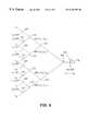
- FIG. 5shows a functional schematic diagram of an 8:1 multiplexor having taps near each input port and having a tap at the single output port.
- signalsare combined 210 , 212 , 214 , 216 , 218 , 220 , and 222 .
- some energy lossis present and the signals are attenuated.
- some unwanted signal lossoccurs at each tap 200 , . . . 207 and 224 , where light is coupled out.
- FIG. 6illustrates an embodiment of the invention that is less expensive to manufacture and wherein unwanted signal loss is reduced.
- a monolithic waveguide chip 310is designed to couple with 8 input signals (or channels) and to multiplex these signals on a single output waveguide within the device.
- Two back-to-back GRIN lenses 320 b and 320 a having a dichroic filter element 325 disposed therebetweenare coupled to the device 310 such that input fibers optically coupled to an input end of the GRIN lens 320 b are optically aligned within corresponding input waveguide ports at the edge of the monolithic waveguide chip 310 .
- the dichroic filter element 325is designed to pass 95% of the light energy of the wavelengths ⁇ 1 to ⁇ 8 incident thereupon, and to reflect 5% of the light to tap ports at the input end face of the lens 320 b .
- One or more fiber tubes not shownmay be used to physically couple the fibers to the GRIN lens 320 b.
- a second pair of back-to-back GRIN lenses 320 a and 320 b having a filter element 325 coupled therebetweenis provided for reflecting backwards 5% of light incident upon it and for passing 95% of the light to an output port. 5% of reflected light is shown to be routed via a waveguide to the input end.
Landscapes
- Physics & Mathematics (AREA)
- General Physics & Mathematics (AREA)
- Optics & Photonics (AREA)
- Engineering & Computer Science (AREA)
- Microelectronics & Electronic Packaging (AREA)
- Optical Couplings Of Light Guides (AREA)
- Optical Integrated Circuits (AREA)
Abstract
Description
Claims (10)
Priority Applications (4)
| Application Number | Priority Date | Filing Date | Title |
|---|---|---|---|
| CA002217688ACA2217688C (en) | 1997-10-07 | 1997-10-07 | Coupling of light into a monolithic waveguide device |
| EP98121476AEP1001288A1 (en) | 1997-10-07 | 1998-11-12 | Coupling of light into a monolithic waveguide device |
| JP10326726AJP2000147309A (en) | 1997-10-07 | 1998-11-17 | Hybrid optical waveguide device |
| US09/204,147US6438291B1 (en) | 1997-10-07 | 1998-12-03 | Coupling of light into a monolithic waveguide device |
Applications Claiming Priority (4)
| Application Number | Priority Date | Filing Date | Title |
|---|---|---|---|
| CA002217688ACA2217688C (en) | 1997-10-07 | 1997-10-07 | Coupling of light into a monolithic waveguide device |
| EP98121476AEP1001288A1 (en) | 1997-10-07 | 1998-11-12 | Coupling of light into a monolithic waveguide device |
| JP10326726AJP2000147309A (en) | 1997-10-07 | 1998-11-17 | Hybrid optical waveguide device |
| US09/204,147US6438291B1 (en) | 1997-10-07 | 1998-12-03 | Coupling of light into a monolithic waveguide device |
Publications (1)
| Publication Number | Publication Date |
|---|---|
| US6438291B1true US6438291B1 (en) | 2002-08-20 |
Family
ID=27427395
Family Applications (1)
| Application Number | Title | Priority Date | Filing Date |
|---|---|---|---|
| US09/204,147Expired - LifetimeUS6438291B1 (en) | 1997-10-07 | 1998-12-03 | Coupling of light into a monolithic waveguide device |
Country Status (4)
| Country | Link |
|---|---|
| US (1) | US6438291B1 (en) |
| EP (1) | EP1001288A1 (en) |
| JP (1) | JP2000147309A (en) |
| CA (1) | CA2217688C (en) |
Cited By (14)
| Publication number | Priority date | Publication date | Assignee | Title |
|---|---|---|---|---|
| US20020164119A1 (en)* | 2001-05-03 | 2002-11-07 | Bryan Michael A. | Integrated gradient index lenses |
| US20040109645A1 (en)* | 2002-12-03 | 2004-06-10 | Alcatel | Thin film filter with waveguide substrate |
| US7492992B1 (en)* | 2003-08-08 | 2009-02-17 | Neophotonics Corporation | Bi-directional PLC transceiver device |
| US9201197B2 (en) | 2013-09-09 | 2015-12-01 | Panduit Corp. | Multi-channel, multi-port optical tap coupler |
| US20170023750A1 (en)* | 2014-04-18 | 2017-01-26 | Source Photonics (Chengdu) Co., Ltd. | NxN PARALLEL OPTICAL TRANSCEIVER |
| US10302859B1 (en) | 2018-06-22 | 2019-05-28 | International Business Machines Corporation | Single edge coupling of chips with integrated waveguides |
| US11063406B1 (en)* | 2020-06-04 | 2021-07-13 | Acacia Communications, Inc. | Configuration for low-ripple optical gain with single-facet semiconductor optical amplifiers |
| CN114077016A (en)* | 2020-08-11 | 2022-02-22 | 美国莫列斯有限公司 | Package structure with photonic integrated circuit |
| WO2022076992A1 (en)* | 2020-10-06 | 2022-04-14 | The Boeing Company | Optical waveguide structure with triple partially overlapping loops |
| US20220229230A1 (en)* | 2019-05-30 | 2022-07-21 | Nippon Telegraph And Telephone Corporation | Optical Multiplexing Circuit and Light Source |
| CN114911002A (en)* | 2022-04-29 | 2022-08-16 | 深圳市砺芯科技有限公司 | Reverse transmission structure of optical waveguide chip |
| US12393094B2 (en) | 2020-10-06 | 2025-08-19 | The Boeing Company | Optical waveguide structure with partially overlapping loops in direction dependent material |
| US12399416B2 (en) | 2020-10-06 | 2025-08-26 | The Boeing Company | Optical waveguide structure with partially overlapping loops in direction dependent material |
| US12442994B2 (en) | 2020-08-11 | 2025-10-14 | Molex, Llc | Package structure having photonic integrated circuit |
Families Citing this family (5)
| Publication number | Priority date | Publication date | Assignee | Title |
|---|---|---|---|---|
| JP2006201313A (en)* | 2005-01-18 | 2006-08-03 | Fuji Xerox Co Ltd | Optical transmission device and optical module |
| CN100412587C (en)* | 2005-12-31 | 2008-08-20 | 中国科学院物理研究所 | Active alignment fixture and method for single-mode lensed fiber and slab ridge waveguide |
| WO2011057812A2 (en)* | 2009-11-16 | 2011-05-19 | Leoni Kabel Holding Gmbh | Optical assembly |
| GB2477740B (en)* | 2010-02-10 | 2014-06-25 | Oclaro Technology Ltd | Reduced length optoelectronic devices |
| US9188745B2 (en) | 2013-09-09 | 2015-11-17 | Panduit Corp. | Multi-channel, multi-port optical tap coupler |
Citations (15)
| Publication number | Priority date | Publication date | Assignee | Title |
|---|---|---|---|---|
| US4693544A (en)* | 1982-12-14 | 1987-09-15 | Nippon Sheet Glass Co., Ltd. | Optical branching device with internal waveguide |
| US4878728A (en) | 1983-12-17 | 1989-11-07 | U.S. Philips Corporation | Multilayer integrated optical device |
| US5009477A (en) | 1989-05-12 | 1991-04-23 | At&T Bell Laboratories | Optical interconnect arrangement |
| US5050954A (en)* | 1990-01-12 | 1991-09-24 | At&T Bell Laboratories | Multiport optical devices |
| US5071216A (en) | 1990-06-28 | 1991-12-10 | Honeywell Inc. | Optical interconnect waveguide-beam coupler |
| US5555330A (en)* | 1994-12-21 | 1996-09-10 | E-Tek Dynamics, Inc. | Wavelength division multiplexed coupler with low crosstalk between channels and integrated coupler/isolator device |
| US5657155A (en)* | 1996-08-16 | 1997-08-12 | Jds Fitel Inc. | Optical tap coupler device |
| GB2315882A (en) | 1996-07-30 | 1998-02-11 | Seiko Giken Kk | Optical device with different diameter optic fibre cores and GRIN lens |
| EP0856764A2 (en) | 1997-01-31 | 1998-08-05 | Jds Fitel Inc. | Grin lensed optical device |
| US5852505A (en)* | 1994-12-28 | 1998-12-22 | Lucent Technologies Inc. | Dense waveguide division multiplexers implemented using a first stage fourier filter |
| US6005995A (en)* | 1997-08-01 | 1999-12-21 | Dicon Fiberoptics, Inc. | Frequency sorter, and frequency locker for monitoring frequency shift of radiation source |
| US6044187A (en)* | 1998-04-01 | 2000-03-28 | Duck; Gary S. | Multi-port fiber optical device |
| US6055347A (en)* | 1997-08-26 | 2000-04-25 | Li; Jinghui | Multi-pass optical filter |
| US6215924B1 (en)* | 1998-08-06 | 2001-04-10 | Optical Coating Laboratory, Inc. | Optical coupler device for dense wavelength division multiplexing |
| EP0729044B1 (en) | 1995-02-21 | 2003-01-29 | Ngk Insulators, Ltd. | Optical fiber-fixing substrate, method of producing the same and optical device |
- 1997
- 1997-10-07CACA002217688Apatent/CA2217688C/ennot_activeExpired - Fee Related
- 1998
- 1998-11-12EPEP98121476Apatent/EP1001288A1/ennot_activeWithdrawn
- 1998-11-17JPJP10326726Apatent/JP2000147309A/enactivePending
- 1998-12-03USUS09/204,147patent/US6438291B1/ennot_activeExpired - Lifetime
Patent Citations (15)
| Publication number | Priority date | Publication date | Assignee | Title |
|---|---|---|---|---|
| US4693544A (en)* | 1982-12-14 | 1987-09-15 | Nippon Sheet Glass Co., Ltd. | Optical branching device with internal waveguide |
| US4878728A (en) | 1983-12-17 | 1989-11-07 | U.S. Philips Corporation | Multilayer integrated optical device |
| US5009477A (en) | 1989-05-12 | 1991-04-23 | At&T Bell Laboratories | Optical interconnect arrangement |
| US5050954A (en)* | 1990-01-12 | 1991-09-24 | At&T Bell Laboratories | Multiport optical devices |
| US5071216A (en) | 1990-06-28 | 1991-12-10 | Honeywell Inc. | Optical interconnect waveguide-beam coupler |
| US5555330A (en)* | 1994-12-21 | 1996-09-10 | E-Tek Dynamics, Inc. | Wavelength division multiplexed coupler with low crosstalk between channels and integrated coupler/isolator device |
| US5852505A (en)* | 1994-12-28 | 1998-12-22 | Lucent Technologies Inc. | Dense waveguide division multiplexers implemented using a first stage fourier filter |
| EP0729044B1 (en) | 1995-02-21 | 2003-01-29 | Ngk Insulators, Ltd. | Optical fiber-fixing substrate, method of producing the same and optical device |
| GB2315882A (en) | 1996-07-30 | 1998-02-11 | Seiko Giken Kk | Optical device with different diameter optic fibre cores and GRIN lens |
| US5657155A (en)* | 1996-08-16 | 1997-08-12 | Jds Fitel Inc. | Optical tap coupler device |
| EP0856764A2 (en) | 1997-01-31 | 1998-08-05 | Jds Fitel Inc. | Grin lensed optical device |
| US6005995A (en)* | 1997-08-01 | 1999-12-21 | Dicon Fiberoptics, Inc. | Frequency sorter, and frequency locker for monitoring frequency shift of radiation source |
| US6055347A (en)* | 1997-08-26 | 2000-04-25 | Li; Jinghui | Multi-pass optical filter |
| US6044187A (en)* | 1998-04-01 | 2000-03-28 | Duck; Gary S. | Multi-port fiber optical device |
| US6215924B1 (en)* | 1998-08-06 | 2001-04-10 | Optical Coating Laboratory, Inc. | Optical coupler device for dense wavelength division multiplexing |
Cited By (33)
| Publication number | Priority date | Publication date | Assignee | Title |
|---|---|---|---|---|
| US20020164119A1 (en)* | 2001-05-03 | 2002-11-07 | Bryan Michael A. | Integrated gradient index lenses |
| US7164818B2 (en)* | 2001-05-03 | 2007-01-16 | Neophontonics Corporation | Integrated gradient index lenses |
| US20070116409A1 (en)* | 2001-05-03 | 2007-05-24 | Neophotonics Corporation | Integrated gradient index lenses |
| US7391940B2 (en) | 2001-05-03 | 2008-06-24 | Neophotonics Corporation | Integrated gradient index lenses |
| US20040109645A1 (en)* | 2002-12-03 | 2004-06-10 | Alcatel | Thin film filter with waveguide substrate |
| US7092601B2 (en)* | 2002-12-03 | 2006-08-15 | Alcatel | Thin film filter with waveguide substrate |
| US7492992B1 (en)* | 2003-08-08 | 2009-02-17 | Neophotonics Corporation | Bi-directional PLC transceiver device |
| US9201197B2 (en) | 2013-09-09 | 2015-12-01 | Panduit Corp. | Multi-channel, multi-port optical tap coupler |
| US20170023750A1 (en)* | 2014-04-18 | 2017-01-26 | Source Photonics (Chengdu) Co., Ltd. | NxN PARALLEL OPTICAL TRANSCEIVER |
| US9709759B2 (en)* | 2014-04-18 | 2017-07-18 | Source Photonics (Chengdu) Co., Ltd. | NxN parallel optical transceiver |
| US10302859B1 (en) | 2018-06-22 | 2019-05-28 | International Business Machines Corporation | Single edge coupling of chips with integrated waveguides |
| US10444429B1 (en)* | 2018-06-22 | 2019-10-15 | International Business Machines Corporation | Single edge coupling of chips with integrated waveguides |
| US20190391330A1 (en)* | 2018-06-22 | 2019-12-26 | International Business Machines Corporation | Single edge coupling of chips with integrated waveguides |
| US10527787B1 (en) | 2018-06-22 | 2020-01-07 | International Business Machines Corporation | Single edge coupling of chips with integrated waveguides |
| US10901147B2 (en) | 2018-06-22 | 2021-01-26 | International Business Machines Corporation | Single edge coupling of chips with integrated waveguides |
| US10901146B2 (en)* | 2018-06-22 | 2021-01-26 | International Business Machines Corporation | Single edge coupling of chips with integrated waveguides |
| US20220229230A1 (en)* | 2019-05-30 | 2022-07-21 | Nippon Telegraph And Telephone Corporation | Optical Multiplexing Circuit and Light Source |
| US12197006B2 (en)* | 2019-05-30 | 2025-01-14 | Nippon Telegraph And Telephone Corporation | Optical multiplexing circuit and light source |
| US11063406B1 (en)* | 2020-06-04 | 2021-07-13 | Acacia Communications, Inc. | Configuration for low-ripple optical gain with single-facet semiconductor optical amplifiers |
| CN114077016B (en)* | 2020-08-11 | 2023-09-01 | 美国莫列斯有限公司 | Package structure with photonic integrated circuit |
| US12442994B2 (en) | 2020-08-11 | 2025-10-14 | Molex, Llc | Package structure having photonic integrated circuit |
| CN114077016A (en)* | 2020-08-11 | 2022-02-22 | 美国莫列斯有限公司 | Package structure with photonic integrated circuit |
| US11988867B2 (en) | 2020-08-11 | 2024-05-21 | Molex, Llc | Package structure having photonic integrated circuit |
| US11614673B2 (en) | 2020-10-06 | 2023-03-28 | The Boeing Company | Nonlinear optical waveguide structures for light generation and conversion |
| US11561454B2 (en) | 2020-10-06 | 2023-01-24 | The Boeing Company | Optical waveguide structure with partially overlapping loops in direction dependent material |
| WO2022076991A1 (en)* | 2020-10-06 | 2022-04-14 | The Boeing Company | Directional phase matching optical waveguide |
| US11614672B2 (en) | 2020-10-06 | 2023-03-28 | The Boeing Company | Optical waveguide structure with triple partially overlapping loops |
| US11550201B2 (en) | 2020-10-06 | 2023-01-10 | The Boeing Company | Directional phase matching optical waveguide |
| WO2022076992A1 (en)* | 2020-10-06 | 2022-04-14 | The Boeing Company | Optical waveguide structure with triple partially overlapping loops |
| US12393094B2 (en) | 2020-10-06 | 2025-08-19 | The Boeing Company | Optical waveguide structure with partially overlapping loops in direction dependent material |
| US12399416B2 (en) | 2020-10-06 | 2025-08-26 | The Boeing Company | Optical waveguide structure with partially overlapping loops in direction dependent material |
| WO2022076993A1 (en)* | 2020-10-06 | 2022-04-14 | The Boeing Company | Nonlinear optical waveguide structures for light generation and conversion |
| CN114911002A (en)* | 2022-04-29 | 2022-08-16 | 深圳市砺芯科技有限公司 | Reverse transmission structure of optical waveguide chip |
Also Published As
| Publication number | Publication date |
|---|---|
| CA2217688C (en) | 2006-12-05 |
| CA2217688A1 (en) | 1999-04-07 |
| JP2000147309A (en) | 2000-05-26 |
| EP1001288A1 (en) | 2000-05-17 |
Similar Documents
| Publication | Publication Date | Title |
|---|---|---|
| US6438291B1 (en) | Coupling of light into a monolithic waveguide device | |
| US7561765B2 (en) | Optical integrated circuit and optical integrated circuit module | |
| US6061481A (en) | Optoelectronic circuit | |
| US6744945B2 (en) | Wavelength multiplexer and optical unit | |
| EP0234369B1 (en) | Optical branching filter | |
| CA2256886C (en) | Method and device for optical coupling | |
| US20100111468A1 (en) | Optical integrated circuit and optical integrated circuit module | |
| JPH04212110A (en) | Electronic and optical module of optical fiber | |
| CA2175886C (en) | Optical wavelength division multiplexer device | |
| US4564755A (en) | Transmission and reception device for a fiber-optical sensor system | |
| EP0947865B1 (en) | Multi-port optical coupler with lens | |
| US6157760A (en) | Two-way optical communication device and two-way optical communication apparatus | |
| JP2005004204A (en) | Optical hybrid module and manufacturing method thereof | |
| EP0463779A1 (en) | Fibre optic waveguide beam splitter | |
| US6845197B2 (en) | Optical tap | |
| JP2002277675A (en) | Optical wave circuit module | |
| JPH05203830A (en) | Optical multiplexer demultiplexer | |
| EP0947861A1 (en) | Hybrid waveguiding optical device | |
| JP3120777B2 (en) | Optical waveguide type signal light monitor device | |
| JP2579092B2 (en) | WDM module for bidirectional optical transmission | |
| JPH05181035A (en) | Optical demultiplexing / branching device | |
| JP2005249966A (en) | Optical member, its manufacturing method, and optical module | |
| JPS63106606A (en) | Optical multiplexer and demultiplexer | |
| KR100513846B1 (en) | Bi-directional transceiver using photonic crystal structures | |
| JPS629305A (en) | optical coupling parts |
Legal Events
| Date | Code | Title | Description |
|---|---|---|---|
| AS | Assignment | Owner name:JDS FITEL INC., CANADA Free format text:ASSIGNMENT OF ASSIGNORS INTEREST;ASSIGNORS:DUCK, GARY;CHENG, YIHAO;INGENHOFF, JAN;AND OTHERS;REEL/FRAME:009629/0510;SIGNING DATES FROM 19981118 TO 19981127 Owner name:INTEGRIERTE OPTIK GMBH, GERMANY Free format text:ASSIGNMENT OF ASSIGNORS INTEREST;ASSIGNORS:DUCK, GARY;CHENG, YIHAO;INGENHOFF, JAN;AND OTHERS;REEL/FRAME:009629/0510;SIGNING DATES FROM 19981118 TO 19981127 | |
| STCF | Information on status: patent grant | Free format text:PATENTED CASE | |
| CC | Certificate of correction | ||
| AS | Assignment | Owner name:JDS UNIPHASE INC., CANADA Free format text:MERGER;ASSIGNOR:JDS FITEL INC.;REEL/FRAME:015676/0001 Effective date:19990706 | |
| FEPP | Fee payment procedure | Free format text:PAYOR NUMBER ASSIGNED (ORIGINAL EVENT CODE: ASPN); ENTITY STATUS OF PATENT OWNER: LARGE ENTITY Free format text:PAYER NUMBER DE-ASSIGNED (ORIGINAL EVENT CODE: RMPN); ENTITY STATUS OF PATENT OWNER: LARGE ENTITY | |
| FPAY | Fee payment | Year of fee payment:4 | |
| AS | Assignment | Owner name:JDS UNIPHASE PHOTONICS GMBH & CO. KG, GERMANY Free format text:CHANGE OF NAME;ASSIGNOR:IOT INTEGRIERTE OPTIK GMBH & CO, KG;REEL/FRAME:019690/0232 Effective date:20000701 | |
| AS | Assignment | Owner name:JDS UNIPHASE CORPORATION, CALIFORNIA Free format text:ASSIGNMENT OF ASSIGNORS INTEREST;ASSIGNOR:JDS UNIPHASE PHOTONICS GMBH I.L.;REEL/FRAME:022939/0443 Effective date:20080715 | |
| FPAY | Fee payment | Year of fee payment:8 | |
| FPAY | Fee payment | Year of fee payment:12 | |
| AS | Assignment | Owner name:JDS UNIPHASE CORPORATION, CALIFORNIA Free format text:ASSIGNMENT OF ASSIGNORS INTEREST;ASSIGNOR:JDS UNIPHASE INC.;REEL/FRAME:036087/0320 Effective date:20150626 | |
| AS | Assignment | Owner name:LUMENTUM OPERATIONS LLC, CALIFORNIA Free format text:ASSIGNMENT OF ASSIGNORS INTEREST;ASSIGNOR:JDS UNIPHASE CORPORATION;REEL/FRAME:036420/0340 Effective date:20150731 | |
| FEPP | Fee payment procedure | Free format text:PAYOR NUMBER ASSIGNED (ORIGINAL EVENT CODE: ASPN); ENTITY STATUS OF PATENT OWNER: LARGE ENTITY Free format text:PAYER NUMBER DE-ASSIGNED (ORIGINAL EVENT CODE: RMPN); ENTITY STATUS OF PATENT OWNER: LARGE ENTITY | |
| AS | Assignment | Owner name:LUMENTUM OPERATIONS LLC, CALIFORNIA Free format text:CORRECTIVE ASSIGNMENT TO CORRECT THE PATENTS LISTED ON PAGE A-A33 PREVIOUSLY RECORDED ON REEL 036420 FRAME 0340. ASSIGNOR(S) HEREBY CONFIRMS THE PATENT NUMBERS 7,868,247 AND 6,476,312 WERE LISTED IN ERROR AND SHOULD BE REMOVED;ASSIGNOR:JDS UNIPHASE CORPORATION;REEL/FRAME:037562/0513 Effective date:20150731 Owner name:LUMENTUM OPERATIONS LLC, CALIFORNIA Free format text:CORRECTIVE ASSIGNMENT TO CORRECT INCORRECT PATENTS 7,868,247 AND 6,476,312 ON PAGE A-A33 PREVIOUSLY RECORDED ON REEL 036420 FRAME 0340. ASSIGNOR(S) HEREBY CONFIRMS THE ASSIGNMENT;ASSIGNOR:JDS UNIPHASE CORPORATION;REEL/FRAME:037562/0513 Effective date:20150731 | |
| AS | Assignment | Owner name:LUMENTUM OPERATIONS LLC, CALIFORNIA Free format text:CORRECTIVE ASSIGNMENT TO CORRECT THE PATENTS LISTED ON PAGE A-A33 PATENT NUMBERS 7,868,247 AND 6,476,312 WERE LISTED IN ERROR AND SHOULD BE REMOVED. PREVIOUSLY RECORDED ON REEL 036420 FRAME 0340. ASSIGNOR(S) HEREBY CONFIRMS THE ASSIGNMENT;ASSIGNOR:JDS UNIPHASE CORPORATION;REEL/FRAME:037627/0641 Effective date:20150731 Owner name:LUMENTUM OPERATIONS LLC, CALIFORNIA Free format text:CORRECTIVE ASSIGNMENT TO CORRECT PATENTS 7,868,247 AND 6,476,312 LISTED ON PAGE A-A33 PREVIOUSLY RECORDED ON REEL 036420 FRAME 0340. ASSIGNOR(S) HEREBY CONFIRMS THE ASSIGNMENT;ASSIGNOR:JDS UNIPHASE CORPORATION;REEL/FRAME:037627/0641 Effective date:20150731 | |
| FEPP | Fee payment procedure | Free format text:PAYOR NUMBER ASSIGNED (ORIGINAL EVENT CODE: ASPN); ENTITY STATUS OF PATENT OWNER: LARGE ENTITY Free format text:PAYER NUMBER DE-ASSIGNED (ORIGINAL EVENT CODE: RMPN); ENTITY STATUS OF PATENT OWNER: LARGE ENTITY | |
| AS | Assignment | Owner name:DEUTSCHE BANK AG NEW YORK BRANCH, AS COLLATERAL AGENT, NEW YORK Free format text:PATENT SECURITY AGREEMENT;ASSIGNORS:LUMENTUM OPERATIONS LLC;OCLARO FIBER OPTICS, INC.;OCLARO, INC.;REEL/FRAME:047788/0511 Effective date:20181210 Owner name:DEUTSCHE BANK AG NEW YORK BRANCH, AS COLLATERAL AG Free format text:PATENT SECURITY AGREEMENT;ASSIGNORS:LUMENTUM OPERATIONS LLC;OCLARO FIBER OPTICS, INC.;OCLARO, INC.;REEL/FRAME:047788/0511 Effective date:20181210 | |
| AS | Assignment | Owner name:OCLARO FIBER OPTICS, INC., CALIFORNIA Free format text:RELEASE BY SECURED PARTY;ASSIGNOR:DEUTSCHE AG NEW YORK BRANCH;REEL/FRAME:051287/0556 Effective date:20191212 Owner name:LUMENTUM OPERATIONS LLC, CALIFORNIA Free format text:RELEASE BY SECURED PARTY;ASSIGNOR:DEUTSCHE AG NEW YORK BRANCH;REEL/FRAME:051287/0556 Effective date:20191212 Owner name:OCLARO, INC., CALIFORNIA Free format text:RELEASE BY SECURED PARTY;ASSIGNOR:DEUTSCHE AG NEW YORK BRANCH;REEL/FRAME:051287/0556 Effective date:20191212 |