US6436768B1 - Source drain implant during ONO formation for improved isolation of SONOS devices - Google Patents
Source drain implant during ONO formation for improved isolation of SONOS devicesDownload PDFInfo
- Publication number
- US6436768B1 US6436768B1US09/893,279US89327901AUS6436768B1US 6436768 B1US6436768 B1US 6436768B1US 89327901 AUS89327901 AUS 89327901AUS 6436768 B1US6436768 B1US 6436768B1
- Authority
- US
- United States
- Prior art keywords
- charge trapping
- layer
- trapping dielectric
- dielectric
- over
- Prior art date
- Legal status (The legal status is an assumption and is not a legal conclusion. Google has not performed a legal analysis and makes no representation as to the accuracy of the status listed.)
- Expired - Lifetime
Links
Images


Classifications
- H—ELECTRICITY
- H01—ELECTRIC ELEMENTS
- H01L—SEMICONDUCTOR DEVICES NOT COVERED BY CLASS H10
- H01L21/00—Processes or apparatus adapted for the manufacture or treatment of semiconductor or solid state devices or of parts thereof
- H01L21/02—Manufacture or treatment of semiconductor devices or of parts thereof
- H01L21/04—Manufacture or treatment of semiconductor devices or of parts thereof the devices having potential barriers, e.g. a PN junction, depletion layer or carrier concentration layer
- H01L21/18—Manufacture or treatment of semiconductor devices or of parts thereof the devices having potential barriers, e.g. a PN junction, depletion layer or carrier concentration layer the devices having semiconductor bodies comprising elements of Group IV of the Periodic Table or AIIIBV compounds with or without impurities, e.g. doping materials
- H01L21/26—Bombardment with radiation
- H01L21/263—Bombardment with radiation with high-energy radiation
- H01L21/265—Bombardment with radiation with high-energy radiation producing ion implantation
- H01L21/26506—Bombardment with radiation with high-energy radiation producing ion implantation in group IV semiconductors
- H01L21/26513—Bombardment with radiation with high-energy radiation producing ion implantation in group IV semiconductors of electrically active species
- H01L21/2652—Through-implantation
- H—ELECTRICITY
- H01—ELECTRIC ELEMENTS
- H01L—SEMICONDUCTOR DEVICES NOT COVERED BY CLASS H10
- H01L21/00—Processes or apparatus adapted for the manufacture or treatment of semiconductor or solid state devices or of parts thereof
- H01L21/02—Manufacture or treatment of semiconductor devices or of parts thereof
- H01L21/04—Manufacture or treatment of semiconductor devices or of parts thereof the devices having potential barriers, e.g. a PN junction, depletion layer or carrier concentration layer
- H01L21/18—Manufacture or treatment of semiconductor devices or of parts thereof the devices having potential barriers, e.g. a PN junction, depletion layer or carrier concentration layer the devices having semiconductor bodies comprising elements of Group IV of the Periodic Table or AIIIBV compounds with or without impurities, e.g. doping materials
- H01L21/26—Bombardment with radiation
- H01L21/263—Bombardment with radiation with high-energy radiation
- H01L21/265—Bombardment with radiation with high-energy radiation producing ion implantation
- H01L21/2658—Bombardment with radiation with high-energy radiation producing ion implantation of a molecular ion, e.g. decaborane
- H—ELECTRICITY
- H10—SEMICONDUCTOR DEVICES; ELECTRIC SOLID-STATE DEVICES NOT OTHERWISE PROVIDED FOR
- H10B—ELECTRONIC MEMORY DEVICES
- H10B43/00—EEPROM devices comprising charge-trapping gate insulators
- H10B43/30—EEPROM devices comprising charge-trapping gate insulators characterised by the memory core region
- H—ELECTRICITY
- H10—SEMICONDUCTOR DEVICES; ELECTRIC SOLID-STATE DEVICES NOT OTHERWISE PROVIDED FOR
- H10D—INORGANIC ELECTRIC SEMICONDUCTOR DEVICES
- H10D30/00—Field-effect transistors [FET]
- H10D30/01—Manufacture or treatment
- H10D30/021—Manufacture or treatment of FETs having insulated gates [IGFET]
- H10D30/0413—Manufacture or treatment of FETs having insulated gates [IGFET] of FETs having charge-trapping gate insulators, e.g. MNOS transistors
Definitions
- the present inventiongenerally relates to fabricating SONOS type nonvolatile memory semiconductor devices.
- the present inventionrelates to improved methods of fabricating the source/drain regions and the charge trapping dielectric of SONOS type nonvolatile memory semiconductor devices.
- EEPROMselectrically erasable programmable read only memory
- a memory cellcharacterized by a vertical stack of a tunnel oxide, a first polysilicon layer over the tunnel oxide, an ONO (oxide-nitride-oxide) interlevel dielectric over the first polysilicon layer, and a second polysilicon layer over the ONO interlevel dielectric.
- ONOoxide-nitride-oxide
- Guterman et alrelates to a floating gate nonvolatile memory cell consisting of a floating gate sandwiched between a gate oxide and an interlevel oxide, with a control gate over the interlevel oxide.
- a flash memory cellis programmed by inducing hot electron injection from a portion of the substrate, such as the channel section near the drain region, to the floating gate. Electron injection carries negative charge into the floating gate.
- the injection mechanismcan be induced by grounding the source region and a bulk portion of the substrate and applying a relatively high positive voltage to the control electrode to create an electron attracting field and applying a positive voltage of moderate magnitude to the drain region in order to generate “hot” (high energy) electrons.
- the negative potential of the floating gateraises the threshold voltage of its field effect transistor (FET) and inhibits current flow through the channel region through a subsequent “read” mode.
- FETfield effect transistor
- the magnitude of the read currentis used to determine whether or not a flash memory cell is programmed.
- the act of discharging the floating gate of a flash memory cellis called the erase function.
- the erase functionis typically carried out by a Fowler-Nordheim tunneling mechanism between the floating gate and the source region of the transistor (source erase or negative gate erase) or between the floating gate and the substrate (channel erase).
- a source erase operationis induced by applying a high positive voltage to the source region and grounding the control gate and the substrate while floating the drain of the respective memory cell.
- SONOSSilicon Oxide Nitride Oxide Silicon
- flash memory cellsare constructed having a charge trapping non-conducting dielectric layer, typically a silicon nitride layer, sandwiched between two silicon dioxide layers (insulating layers).
- the nonconducting dielectric layerfunctions as an electrical charge trapping medium.
- a conducting gate layeris placed over the upper silicon dioxide layer. Since the electrical charge is trapped locally near whichever side that is used as the drain, this structure can be described as a two-transistor cell, or two-bits per cell. If multi-level is used, then four or more bits per cell can be accomplished.
- Multi-bit cellsenable SONOS type memory devices to have the advantage over others in facilitating the continuing trend increasing the amount of information held/processed on an integrated circuit chip.
- each bitis read in a direction opposite that in which it is programmed with a relatively low gate voltage.
- the right bitis programmed conventionally by applying programming voltages to the gate and the drain while the source is grounded or at a lower voltage. Hot electrons are accelerated sufficiently so that they are injected into a region of the trapping dielectric layer near the drain.
- the deviceis read in the opposite direction from which it is written, meaning voltages are applied to the gate and the source while the drain is grounded or at a lower voltage.
- the left bitis similarly programmed and read by swapping the functionality of source and drain terminals. Programming one of the bits leaves the other bit with its information intact.
- Reading in the reverse directionis most effective when relatively low gate voltages are used.
- a benefit of utilizing relatively low gate voltages in combination with reading in the reverse directionis that the potential drop across the portion of the channel beneath the trapped charge region is significantly reduced.
- a relatively small programming region or charge trapping regionis possible due to the lower channel potential drop under the charge trapping region. This permits much faster programming times because the effect of the charge trapped in the localized trapping region is amplified. Programming times are reduced while the delta in threshold voltage between the programmed versus unprogrammed states remains the same as when the device is read in the forward direction.
- SONOS type memory devicesoffer additional advantages as well.
- the erase mechanism of the memory cellis greatly enhanced. Both bits of the memory cell can be erased by applying suitable erase voltages to the gate and the drain for the right bit and to the gate and the source for the left bit.
- Another advantageincludes reduced wearout from cycling thus increasing device longevity.
- An effect of reading in the reverse directionis that a much higher threshold voltage for the same amount of programming is possible.
- a much smaller region of trapped chargeis required when the cell is read in the reverse direction than when the cell is read in the forward direction.
- the erase mechanismis enhanced when the charge trapping region is made as narrow as possible. Programming in the forward direction and reading in the reverse direction permits limiting the width of the charge trapping region to a narrow region near the drain (right bit) or the source. This allows for much more efficient erasing of the memory cell.
- Another advantage of localized charge trappingis that during erase, the region of the nitride away from the drain does not experience deep depletion since the erase occurs near the drain only.
- the final threshold of the cell after erasingis self limited by the device structure itself. This is in direct contrast to conventional single transistor floating gate flash memory cells which often have deep depletion problems.
- a well formed ONO dielectricprovides adequate poly to source/drain isolation. Contamination and dopants/implants that undesirably become incorporated into an ONO dielectric decrease the poly to source/drain isolation, thereby decreasing the reliability of the memory devices made therewith. This is especially a concern if attempts are made to form bitlines by implanting source/drains after the ONO dielectric is formed. However, if the source/drains are implanted prior to forming the ONO dielectric, unwanted excessive diffusion of the implants occurs. This is because there are several thermal cycles associated with making and annealing the ONO dielectric. There is an unmet need for SONOS type nonvolatile memory devices having both improved poly to source/drain isolation and little or no excessive diffusion of implants.
- the present inventionprovides a simplified process for fabricating SONOS type nonvolatile memory devices, and in particular, a simplified process for forming charge trapping dielectrics and source/drains in SONOS type nonvolatile memory devices.
- the SONOS type nonvolatile memory deviceslead to the efficient production of dense, robust single-poly nonvolatile memory devices.
- the present inventionminimizes defects, contamination, and cost commonly associated with ONO formation in the core region, improves poly to source/drain isolation, and mitigates excessive diffusion of source/drain implants.
- the present inventionalso leads to the formation of charge trapping dielectrics having uniform and precise thickness while improved scaling.
- One aspect of the present inventionrelates to a method of forming a SONOS type non-volatile semiconductor memory device, involving forming a first layer of a charge trapping dielectric on a semiconductor substrate; forming a second layer of the charge trapping dielectric over the first layer of the charge trapping dielectric on the semiconductor substrate; optionally at least partially forming a third layer of the charge trapping dielectric over the second layer of the charge trapping dielectric on the semiconductor substrate; optionally removing the third layer of the charge trapping dielectric, if present; forming a source/drain mask over the charge trapping dielectric; implanting a source/drain implant through the charge trapping dielectric into the semiconductor substrate; optionally removing the third layer of the charge trapping dielectric, if present; and one of forming the third layer of the charge trapping dielectric over the second layer of the charge trapping dielectric on the semiconductor substrate, reforming the third layer of the charge trapping dielectric over the second layer of the charge trapping dielectric on the semiconductor substrate, or forming additional
- FIG. 1illustrates a cross-sectional view of a SONOS type memory cell in accordance with one aspect of the invention.
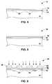
- FIG. 2illustrates a cross-sectional view of a first method of forming a SONOS type nonvolatile memory device in accordance with one aspect of the present invention.
- FIG. 3illustrates another cross-sectional view of a first method of forming a SONOS type nonvolatile memory device in accordance with one aspect of the present invention.
- FIG. 4illustrates yet another cross-sectional view of a first method of forming a SONOS type nonvolatile memory device in accordance with one aspect of the present invention.
- FIG. 5illustrates a cross-sectional view of a second method of forming a SONOS type nonvolatile memory device in accordance with one aspect of the present invention.
- FIG. 6illustrates another cross-sectional view of a second method of forming a SONOS type nonvolatile memory device in accordance with one aspect of the present invention.
- FIG. 7illustrates yet another cross-sectional view of a second method of forming a SONOS type nonvolatile memory device in accordance with one aspect of the present invention.
- FIG. 8illustrates still yet another cross-sectional view of a second method of forming a SONOS type nonvolatile memory device in accordance with one aspect of the present invention.
- FIG. 9illustrates a cross-sectional view of a third method of forming a SONOS type nonvolatile memory device in accordance with one aspect of the present invention.
- FIG. 10illustrates another cross-sectional view of a third method of forming a SONOS type nonvolatile memory device in accordance with one aspect of the present invention.
- FIG. 11illustrates yet another cross-sectional view of a third method of forming a SONOS type nonvolatile memory device in accordance with one aspect of the present invention.
- FIG. 12illustrates a cross-sectional view of a fourth method of forming a SONOS type nonvolatile memory device in accordance with one aspect of the present invention.
- FIG. 13illustrates another cross-sectional view of a fourth method of forming a SONOS type nonvolatile memory device in accordance with one aspect of the present invention.
- FIG. 14illustrates yet another cross-sectional view of a fourth method of forming a SONOS type nonvolatile memory device in accordance with one aspect of the present invention.
- FIG. 15illustrates still yet another cross-sectional view of a second method of forming a SONOS type nonvolatile memory device in accordance with one aspect of the present invention.
- cascading rangesare employed. It is understood that the high or low figure of one of such cascading ranges may be used with the high or low figure of another of such cascading ranges.
- the present inventioninvolves a process for fabricating SONOS type nonvolatile memory devices, and in particular, an improved process for forming the source/drain regions and the charge trapping dielectric in SONOS type nonvolatile memory devices.
- the SONOS type memory cellshave an improved poly to source/drain isolation, little or no excessive diffusion of source/drain implants, and/or a charge trapping dielectric with precise thickness and minimal, if any, defects or contamination.
- the charge trapping dielectricfunctions by storing one or two bits therein. Since the charge storage features of the charge trapping dielectric influence the quality and reliability of SONOS type nonvolatile memory devices, it is important to properly form the charge trapping dielectric.
- the present inventionprovides SONOS type memory cells having charge trapping dielectrics with precise thickness and minimal defects by forming source/drain regions and the charge trapping dielectric using a source/drain mask and/or forming at least additional top layer of the charge trapping dielectric (typically the top oxide layer).
- the present inventioninvolves forming or partially forming the charge trapping dielectric over at least the core region of a memory substrate.
- Partially forming the charge trapping dielectricinvolves partially or not completely forming the top layer, such as not completely forming the top oxide of an ONO charge trapping dielectric.
- the top layermay be partially formed or not formed at all. If present, the top layer of the charge trapping dielectric or partially formed charge trapping dielectric is optionally removed. Source/drain implants are implanted into the core region of the substrate. If present, the top layer of the charge trapping dielectric or partially formed charge trapping dielectric is optionally removed. A new or additional top layer material is formed to provide a charge trapping dielectric over the source/drain implanted core region. As a result, an improved poly to source/drain isolation is provided, as well as mitigation of excessive source/drain diffusion that is typically caused by forming the charge trapping layer after the source/drain implant is performed.
- a SONOS type memory cellis shown.
- a charge trapping dielectric 4is positioned over the silicon substrate 3
- a poly layer 5is positioned over the charge trapping dielectric 4 .
- Source 6 and drain 7 regionsare positioned within the substrate 3 near the edges of the cell 2 .
- the charge trapping dielectric 4contains three layers; namely, a first silicon dioxide layer, a silicon nitride layer, and a second silicon dioxide layer (an ONO charge trapping dielectric). Particularly in the case of an ONO dielectric, the electron trapping is in the silicon nitride layer.
- the charge trapping dielectricmay be any dielectric layer or layers that are capable of or facilitate electron trapping.
- the charge trapping dielectrichas a layer with a lower barrier height than the layers sandwiching it (two layers with relatively higher barrier heights sandwiching a layer with a relatively lower barrier height).
- the oxide layershave a barrier height of about 3.1 eV whereas the nitride layer has a barrier height of about 2.1 eV. In this connection, a well is created in the middle layer.
- charge trapping dielectricsinclude an ONO trilayer dielectric, an oxide/nitride bilayer dielectric, a nitride/oxide bilayer dielectric, an oxide/tantalum oxide bilayer dielectric (SiO 2 /Ta 2 /O 5 ), an oxide/tantalum oxide/oxide trilayer dielectric (SiO 2 /Ta 2 O 5 /SiO 2 ), an oxide/strontium titanate bilayer dielectric (SiO 2 /SrTiO 3 ), an oxide/barium strontium titanate bilayer dielectric (SiO 2 /BaSrTiO 2 ), an oxide/strontium titanate/oxide trilayer dielectric (SiO 2 /SrTiO 3 /SiO 2 ), an oxide/strontium titanate/barium strontium titanate trilayer dielectric (SiO 2 /SrTiO 3 /SiO 2 ), an oxide/strontium titanate/barium str
- a SONOS type nonvolatile memory devicemay contain any of the charge trapping dielectrics described above.
- a SONOS type nonvolatile memory devicecontains any dielectric layer or layers that are capable of or facilitate electron trapping, and the SONOS type nonvolatile memory device contains an ONO charge trapping dielectric only when a specific reference to such dielectric is indicated.
- one or both of the silicon dioxide layersmay be a silicon-rich silicon dioxide layer.
- One or both of the silicon dioxide layersmay also be an oxygen-rich silicon dioxide layer.
- One or both of the silicon dioxide layersmay be a thermally grown or a deposited oxide.
- One or both of the silicon dioxide layersmay be nitrided oxide layers.
- the nitridemay be a silicon-rich silicon nitride layer or a silicon nitride containing oxygen.
- the nitridemay also be an nitrogen-rich silicon nitride layer.
- the charge trapping dielectric 16has a thickness from about 75 ⁇ to about 300 ⁇ . In another embodiment, the charge trapping dielectric 16 has a thickness from about 100 ⁇ to about 275 ⁇ . In yet another embodiment, the charge trapping dielectric 16 has a thickness from about 110 ⁇ to about 250 ⁇ .
- the oxide layersindividually have thicknesses from about 50 ⁇ to about 150 ⁇ while the nitride layer has a thickness from about 20 ⁇ to about 100 ⁇ . In another embodiment, the oxide layers individually have thicknesses from about 60 ⁇ to about 140 ⁇ while the nitride layer has a thickness from about 25 ⁇ to about 95 ⁇ . In yet another embodiment, the oxide layers individually have thicknesses from about 70 ⁇ to about 130 ⁇ while the nitride layer has a thickness from about 30 ⁇ to about 90 ⁇ .
- FIGS. 2 to 4one aspect of the present invention is specifically described.
- a semiconductor structure 10is shown.
- Semiconductor substrate 12contains two regions, the core region containing the memory cells and the periphery region containing the rest of the chip such as the controlling logic and input/output devices. Processing activity in the core region is highlighted in FIGS. 2 to 4 .
- a silicon dioxide layer 14is formed over the silicon substrate 12 .
- the silicon dioxide layer 14is provided using any suitable means, such as chemical vapor deposition (CVD), including low pressure chemical vapor deposition (LPCVD) and plasma enhanced chemical vapor deposition (PECVD), dry oxidation, wet oxidation or rapid thermal oxidation.
- CVDchemical vapor deposition
- PECVDplasma enhanced chemical vapor deposition
- a silicon nitride layer 16is formed over the silicon dioxide layer 14 .
- the silicon nitride layer 16is provided using any suitable means, such as CVD, including LPCVD and PECVD.
- a source/drain mask 18is provided over the silicon nitride layer 16 by any suitable means.
- a photoresistmay be used to cover portions of the core region while leaving exposed the regions of the substrate to which a source/drain implant is incorporated. That is, a photoresist is deposited over the substrate 12 and patterned to form a source/drain mask 18 (areas of the partially formed charge trapping dielectric directly over the subsequently formed buried bitlines are exposed by the patterned photoresist). In this aspect of the invention, all or substantially all of the periphery region (not shown) of the substrate 12 is masked.
- ionsare implanted into the substrate 12 , as shown by the arrows, forming implanted regions 20 in the substrate 12 directly below openings in the patterned photoresist.
- the semiconductor structure 10is optionally annealed at a suitable temperature after implantation.
- One or more suitable implantation materialsmay be employed. The selection of implantation materials primarily depends on the type of device desired, for example, whether a p-type or n-type is used. Examples of implantation materials include one or more of arsenic, boron, BF 2 ⁇ , antimony, indium, and phosphorus. In one embodiment, an n-type dopant is employed for implantation. In another embodiment, a p-type dopant is employed for implantation. Implantation is conducted to achieve a suitable dosage.
- the implantation materialsare implanted at a dosage suitable to form source/drain regions in the substrate 12 .
- the implantation materialsare implanted at a dosage from about 1 ⁇ 10 14 to about 1 ⁇ 10 16 atoms/cm 2 .
- the implantation materialsare implanted at a dosage from about 5 ⁇ 10 14 to about 7 ⁇ 10 15 atoms/cm 2 .
- the implantation materialsare implanted at a dosage from about 1 ⁇ 10 15 to about 5 ⁇ 10 15 atoms/cm 2 .
- Implanted regions 20form the source/drains of the memory cells in the resultant SONOS type nonvolatile memory device.
- the width of the implanted regions 20at least substantially corresponds to the width of the openings in the source/drain mask 18 .
- the width of the implanted regions 20 (and the subsequently formed source/drains)is from about 0.1 ⁇ m to about 1.5 ⁇ m.
- the width of the implanted regions 20is from about 0.12 ⁇ m to about 1 ⁇ m.
- the width of the implanted regions 20is from about 0.14 ⁇ m to about 0.75 ⁇ m.
- the source/drain mask 18is stripped or removed from the structure 10 .
- the silicon nitride layer 16is optionally cleaned.
- another silicon dioxide layer 22is formed over silicon nitride layer 16 .
- the silicon dioxide layer 22is provided using any suitable means, such as CVD, including LPCVD and PECVD, dry oxidation, wet oxidation or rapid thermal oxidation.
- the second silicon dioxide layer 22is formed in the same manner or a different manner as the first silicon dioxide layer 14 .
- SONOS type flash memory devicesfurther processing is performed to complete the fabrication of SONOS type flash memory devices. For example, polysilicon gates/wordlines are formed over the structure, periphery source/drain regions and gates are doped, spacers are formed, salicidation, completion of formation of SONOS type flash memory cells, select gates, high voltage gates, and low voltage gates, and so on. Using peripheral decoders and control circuitry, each memory cell formed in the core region can be addressed for programming, reading or erasing functions.
- FIGS. 5 to 8another aspect of the present invention is specifically described.
- a semiconductor structure 30is shown.
- Semiconductor substrate 32contains two regions, the core region containing the memory cells and the periphery region containing the rest of the chip such as the controlling logic and input/output devices. Processing activity in the core region is highlighted in FIGS. 5 to 8 .
- a silicon dioxide layer 34is formed over the silicon substrate 32 .
- the silicon dioxide layer 34is provided using any suitable means, such as CVD, including LPCVD and PECVD, dry oxidation, wet oxidation or rapid thermal oxidation.
- a silicon nitride layer 36is formed over the silicon dioxide layer 34 .
- the silicon nitride layer 36is provided using any suitable means, such as CVD, including LPCVD and PECVD.
- Another silicon dioxide layer 38is formed over silicon nitride layer 36 .
- the silicon dioxide layer 38is provided using any suitable means, such as CVD, including LPCVD and PECVD, dry oxidation, wet oxidation or rapid thermal oxidation.
- the second silicon dioxide layer 38is formed in the same manner or a different manner as the first silicon dioxide layer 34 .
- the second silicon dioxide layer 38is fully or partially formed.
- a source/drain mask 40is provided over the second silicon dioxide layer 38 by any suitable means.
- a photoresistmay be used to cover portions of the core region while leaving exposed the regions of the substrate to which a source/drain implant is incorporated. That is, a photoresist is deposited over the substrate 32 and patterned to form a source/drain mask 40 (areas of the fully or partially formed charge trapping dielectric directly over the subsequently formed buried bitlines are exposed by the patterned photoresist). In this aspect of the invention, all or substantially all of the periphery region (not shown) of the substrate 32 is masked.
- ionsare implanted into the substrate 32 , as shown by the arrows, forming implanted regions 42 in the substrate 32 directly below openings in the patterned photoresist.
- the semiconductor structure 30is optionally annealed at a suitable temperature after implantation.
- One or more suitable implantation materialsmay be employed. The selection of implantation materials primarily depends on the type of device desired, for example, whether a p-type or n-type is used. Examples of implantation materials include one or more of arsenic, boron, BF 2 ⁇ , antimony, indium, and phosphorus. In one embodiment, an n-type dopant is employed for implantation. In another embodiment, a p-type dopant is employed for implantation. Implantation is conducted to achieve a suitable dosage.
- the implantation materialsare implanted at a dosage suitable to form source/drain regions in the substrate 32 .
- the implantation materialsare implanted at a dosage from about 1 ⁇ 10 14 to about 1 ⁇ 10 16 atoms/cm 2 .
- the implantation materialsare implanted at a dosage from about 5 ⁇ 10 14 to about 7 ⁇ 10 15 atoms/cm 2 .
- the implantation materialsare implanted at a dosage from about 1 ⁇ 10 15 to about 5 ⁇ 10 15 atoms/cm 2 .
- Implanted regions 42form the source/drains of the memory cells in the resultant SONOS type nonvolatile memory device.
- the width of the implanted regions 42at least substantially corresponds to the width of the openings in the source/drain mask 40 .
- the width of the implanted regions 42 (and the subsequently formed source/drains)is from about 0.1 ⁇ m to about 1.5 ⁇ m.
- the width of the implanted regions 42is from about 0.12 ⁇ m to about 1 ⁇ m.
- the width of the implanted regions 42is from about 0.14 ⁇ m to about 0.75 ⁇ m.
- the source/drain mask 40is stripped or removed from the structure 30 .
- the second silicon dioxide layer 38is optionally cleaned.
- the second silicon dioxide layer 38is removed from the structure by any suitable means. Wet etching, dry etching, plasma etching, or acidic etching may be employed to remove the second silicon dioxide layer 38 from the structure 30 .
- the silicon nitride layer 36is optionally cleaned.
- another silicon dioxide layer 44is formed over silicon nitride layer 36 .
- the silicon dioxide layer 44is provided using any suitable means, such as CVD, including LPCVD and PECVD, dry oxidation, wet oxidation or rapid thermal oxidation.
- the third silicon dioxide layer 44is formed in the same manner or a different manner as the first silicon dioxide layer 34 .
- SONOS type flash memory devicesfurther processing is performed to complete the fabrication of SONOS type flash memory devices. For example, polysilicon gates/wordlines are formed over the structure, periphery source/drain regions and gates are doped, spacers are formed, salicidation, completion of formation of SONOS type flash memory cells, select gates, high voltage gates, and low voltage gates, and so on. Using peripheral decoders and control circuitry, each memory cell formed in the core region can be addressed for programming, reading or erasing functions.
- FIGS. 9 to I 1yet another aspect of the present invention is specifically described.
- a semiconductor structure 50is shown.
- Semiconductor substrate 52contains two regions, the core region containing the memory cells and the periphery region containing the rest of the chip such as the controlling logic and input/output devices. Processing activity in the core region is highlighted in FIGS. 9 to 11 .
- a silicon dioxide layer 54is formed over the silicon substrate 52 .
- the silicon dioxide layer 54is provided using any suitable means, such as CVD, including LPCVD and PECVD, dry oxidation, wet oxidation or rapid thermal oxidation.
- a silicon nitride layer 56is formed over the silicon dioxide layer 54 .
- the silicon nitride layer 56is provided using any suitable means, such as CVD, including LPCVD and PECVD.
- Another silicon dioxide layer 58is formed over silicon nitride layer 56 .
- the silicon dioxide layer 58is provided using any suitable means, such as CVD, including LPCVD and PECVD, dry oxidation, wet oxidation or rapid thermal oxidation.
- the second silicon dioxide layer 58is formed in the same manner or a different manner as the first silicon dioxide layer 54 .
- the second silicon dioxide layer 58is fully or partially formed.
- a source/drain mask 60is provided over the second silicon dioxide layer 58 by any suitable means.
- a photoresistmay be used to cover portions of the core region while leaving exposed the regions of the substrate to which a source/drain implant is incorporated. That is, a photoresist is deposited over the substrate 52 and patterned to form a source/drain mask 60 (areas of the fully or partially formed charge trapping dielectric directly over the subsequently formed buried bitlines are exposed by the patterned photoresist). In this aspect of the invention, all or substantially all of the periphery region (not shown) of the substrate 52 is masked.
- ionsare implanted into the substrate 52 , as shown by the arrows, forming implanted regions 62 in the substrate 52 directly below openings in the patterned photoresist.
- the semiconductor structure 50is optionally annealed at a suitable temperature after implantation.
- One or more suitable implantation materialsmay be employed. The selection of implantation materials primarily depends on the type of device desired, for example, whether a p-type or n-type is used. Examples of implantation materials include one or more of arsenic, boron, BF 2 + , antimony, indium, and phosphorus. In one embodiment, an n-type dopant is employed for implantation. In another embodiment, a p-type dopant is employed for implantation. Implantation is conducted to achieve a suitable dosage.
- the implantation materialsare implanted at a dosage suitable to form source/drain regions in the substrate 52 .
- the implantation materialsare implanted at a dosage from about 1 ⁇ 10 14 to about 1 ⁇ 10 16 atoms/cm 2 .
- the implantation materialsare implanted at a dosage from about 5 ⁇ 10 14 to about 7 ⁇ 10 15 atoms/cm 2 .
- the implantation materialsare implanted at a dosage from about 1 ⁇ 10 15 to about 5 ⁇ 10 15 atoms/cm 2 .
- Implanted regions 62form the source/drains of the memory cells in the resultant SONOS type nonvolatile memory device.
- the width of the implanted regions 62at least substantially corresponds to the width of the openings in the source/drain mask 60 .
- the width of the implanted regions 62 (and the subsequently formed source/drains)is from about 0.1 ⁇ m to about 1.5 ⁇ m.
- the width of the implanted regions 62is from about 0.12 ⁇ m to about 1 ⁇ m.
- the width of the implanted regions 62is from about 0.14 ⁇ m to about 0.75 ⁇ m.
- the source/drain mask 60is stripped or removed from the structure 50 .
- the second silicon dioxide layeris optionally cleaned.
- Additional silicon dioxide materialis formed over the second silicon dioxide layer to provide silicon dioxide layer 64 over silicon nitride layer 56 .
- the additional silicon dioxide material used to form the silicon dioxide layer 64is provided using any suitable means, such as CVD, including LPCVD and PECVD, dry oxidation, wet oxidation or rapid thermal oxidation.
- the additional silicon dioxide materialis provided in the same manner or a different manner as the first silicon dioxide layer 54 and/or in the same manner or a different manner as the second silicon dioxide layer 58 .
- FIGS. 12 to 15still yet another aspect of the present invention is specifically described.
- a semiconductor structure 70is shown.
- Semiconductor substrate 72contains two regions, the core region containing the memory cells and the periphery region containing the rest of the chip such as the controlling logic and input/output devices. Processing activity in the core region is highlighted in FIGS. 12 to 15 .
- a silicon dioxide layer 74is formed over the silicon substrate 72 .
- the silicon dioxide layer 74is provided using any suitable means, such as CVD, including LPCVD and PECVD, dry oxidation, wet oxidation or rapid thermal oxidation.
- a silicon nitride layer 76is formed over the silicon dioxide layer 74 .
- the silicon nitride layer 76is provided using any suitable means, such as CVD, including LPCVD and PECVD.
- Another silicon dioxide layer 78is formed over silicon nitride layer 76 .
- the silicon dioxide layer 78is provided using any suitable means, such as CVD, including LPCVD and PECVD, dry oxidation, wet oxidation or rapid thermal oxidation.
- the second silicon dioxide layer 78is formed in the same manner or a different manner as the first silicon dioxide layer 74 .
- the second silicon dioxide layer 78is fully or partially formed.
- the second silicon dioxide layer 78which is fully or partially formed, is removed or stripped from the structure by any suitable means. Wet etching, dry etching, plasma etching, or acidic etching may be employed to remove the second silicon dioxide layer 78 from the structure 70 . After removing the second silicon dioxide layer 78 , the silicon nitride layer 76 is optionally cleaned.
- a source/drain mask 80is provided over the silicon nitride layer 76 by any suitable means.
- a photoresistmay be used to cover portions of the core region while leaving exposed the regions of the substrate to which a source/drain implant is incorporated. That is, a photoresist is deposited over the substrate 72 and patterned to form a source/drain mask 80 (areas of the partially formed charge trapping dielectric directly over the subsequently formed buried bitlines are exposed by the patterned photoresist). In this aspect of the invention, all or substantially all of the periphery region (not shown) of the substrate 72 is masked.
- ionsare implanted into the substrate 72 , as shown by the arrows, forming implanted regions 82 in the substrate 72 directly below openings in the patterned photoresist.
- the semiconductor structure 70is optionally annealed at a suitable temperature after implantation.
- One or more suitable implantation materialsmay be employed. The selection of implantation materials primarily depends on the type of device desired, for example, whether a p-type or n-type is used. Examples of implantation materials include one or more of arsenic, boron, BF 2 ⁇ , antimony, indium, and phosphorus. In one embodiment, an n-type dopant is employed for implantation. In another embodiment, a p-type dopant is employed for implantation. Implantation is conducted to achieve a suitable dosage.
- the implantation materialsare implanted at a dosage suitable to form source/drain regions in the substrate 72 .
- the implantation materialsare implanted at a dosage from about 1 ⁇ 10 14 to about 1 ⁇ 10 16 atoms/cm 2 .
- the implantation materialsare implanted at a dosage from about 5 ⁇ 10 14 to about 7 ⁇ 10 15 atoms/cm 2 .
- the implantation materialsare implanted at a dosage from about 1 ⁇ 10 15 to about 5 ⁇ 10 15 atoms/cm 2 .
- Implanted regions 82form the source/drains of the memory cells in the resultant SONOS type nonvolatile memory device.
- the width of the implanted regions 82at least substantially corresponds to the width of the openings in the source/drain mask 80 .
- the width of the implanted regions 82 (and the subsequently formed source/drains)is from about 0.1 ⁇ m to about 1.5 ⁇ m.
- the width of the implanted regions 82is from about 0.12 ⁇ m to about 1 ⁇ m.
- the width of the implanted regions 82is from about 0.14 ⁇ m to about 0.75 ⁇ m.
- the source/drain mask 80is stripped or removed from the structure 70 .
- the silicon nitride layer 76is optionally cleaned.
- another silicon dioxide layer 84is formed over silicon nitride layer 76 .
- the silicon dioxide layer 84is provided using any suitable means, such as CVD, including LPCVD and PECVD, dry oxidation, wet oxidation or rapid thermal oxidation.
- the second silicon dioxide layer 84is formed in the same manner or a different manner as the first silicon dioxide layer 74 .
- SONOS type flash memory devicesfurther processing is performed to complete the fabrication of SONOS type flash memory devices. For example, polysilicon gates/wordlines are formed over the structure, periphery source/drain regions and gates are doped, spacers are formed, salicidation, completion of formation of SONOS type flash memory cells, select gates, high voltage gates, and low voltage gates, and so on. Using peripheral decoders and control circuitry, each memory cell formed in the core region can be addressed for programming, reading or erasing functions.
Landscapes
- Physics & Mathematics (AREA)
- Engineering & Computer Science (AREA)
- High Energy & Nuclear Physics (AREA)
- Condensed Matter Physics & Semiconductors (AREA)
- Toxicology (AREA)
- Health & Medical Sciences (AREA)
- General Physics & Mathematics (AREA)
- Manufacturing & Machinery (AREA)
- Computer Hardware Design (AREA)
- Microelectronics & Electronic Packaging (AREA)
- Power Engineering (AREA)
- Spectroscopy & Molecular Physics (AREA)
- Non-Volatile Memory (AREA)
- Semiconductor Memories (AREA)
Abstract
Description
Claims (22)
Priority Applications (6)
| Application Number | Priority Date | Filing Date | Title |
|---|---|---|---|
| US09/893,279US6436768B1 (en) | 2001-06-27 | 2001-06-27 | Source drain implant during ONO formation for improved isolation of SONOS devices |
| EP01996286AEP1399965B1 (en) | 2001-06-27 | 2001-12-14 | Isolation of sonos devices |
| DE60143856TDE60143856D1 (en) | 2001-06-27 | 2001-12-14 | SONOS COMPONENTS INSULATION |
| PCT/US2001/049047WO2003003451A1 (en) | 2001-06-27 | 2001-12-14 | Isolation of sonos devices |
| JP2003509528AJP4885420B2 (en) | 2001-06-27 | 2001-12-14 | Source / drain implantation during ONO formation to improve isolation of SONOS type devices |
| TW091109752ATW550786B (en) | 2001-06-27 | 2002-05-10 | Source drain implant during ONO formation for improved isolation of SONOS devices |
Applications Claiming Priority (1)
| Application Number | Priority Date | Filing Date | Title |
|---|---|---|---|
| US09/893,279US6436768B1 (en) | 2001-06-27 | 2001-06-27 | Source drain implant during ONO formation for improved isolation of SONOS devices |
Publications (1)
| Publication Number | Publication Date |
|---|---|
| US6436768B1true US6436768B1 (en) | 2002-08-20 |
Family
ID=25401319
Family Applications (1)
| Application Number | Title | Priority Date | Filing Date |
|---|---|---|---|
| US09/893,279Expired - LifetimeUS6436768B1 (en) | 2001-06-27 | 2001-06-27 | Source drain implant during ONO formation for improved isolation of SONOS devices |
Country Status (6)
| Country | Link |
|---|---|
| US (1) | US6436768B1 (en) |
| EP (1) | EP1399965B1 (en) |
| JP (1) | JP4885420B2 (en) |
| DE (1) | DE60143856D1 (en) |
| TW (1) | TW550786B (en) |
| WO (1) | WO2003003451A1 (en) |
Cited By (86)
| Publication number | Priority date | Publication date | Assignee | Title |
|---|---|---|---|---|
| US20030082871A1 (en)* | 2001-10-31 | 2003-05-01 | Eliyahou Harari | Multi-state non-volatile integrated circuit memory systems that employ dielectric storage elements |
| US20030109093A1 (en)* | 2001-10-31 | 2003-06-12 | Eliyahou Harari | Multi-state non-volatile integrated circuit memory systems that employ dielectric storage elements |
| US20040023451A1 (en)* | 2001-08-09 | 2004-02-05 | Chang-Hyun Lee | Non-volatile memory device having floating trap type memory cell and method of forming the same |
| US6730564B1 (en)* | 2002-08-12 | 2004-05-04 | Fasl, Llc | Salicided gate for virtual ground arrays |
| US20040121544A1 (en)* | 2002-12-24 | 2004-06-24 | Kent Kuohua Chang | High-k tunneling dielectric for read only memory device and fabrication method thereof |
| DE10259783A1 (en)* | 2002-12-19 | 2004-07-15 | Infineon Technologies Ag | Method for improving process step sequence in forming semiconductor memories with charge trapping memory cells, used same masks as used for forming doped troughs outside memory cell field for removing HV gate dielectric |
| WO2004079824A3 (en)* | 2003-03-05 | 2004-10-28 | Spansion Llc | Charge-trapping memory arrays |
| US6834013B2 (en)* | 2001-12-04 | 2004-12-21 | Macronix International Co., Ltd. | Method for programming and erasing non-volatile memory with nitride tunneling layer |
| US6872609B1 (en) | 2004-01-12 | 2005-03-29 | Advanced Micro Devices, Inc. | Narrow bitline using Safier for mirrorbit |
| US6878988B1 (en) | 2004-06-02 | 2005-04-12 | United Microelectronics Corp. | Non-volatile memory with induced bit lines |
| US20050079674A1 (en)* | 2003-10-09 | 2005-04-14 | Chartered Semiconductor Manufacturing Ltd. | Multi-level gate SONOS flash memory device with high voltage oxide and method for the fabrication thereof |
| US20050142801A1 (en)* | 2003-12-30 | 2005-06-30 | Dongbuanam Semiconductor Inc. | Method for manufacturing semiconductor device |
| US20050141324A1 (en)* | 2003-12-29 | 2005-06-30 | Jae-Bum Ko | Semiconductor memory device for high speed data access |
| US20050153508A1 (en)* | 2004-01-12 | 2005-07-14 | Lingunis Emmanuil H. | Pocket implant for complementary bit disturb improvement and charging improvement of SONOS memory cell |
| US20050169055A1 (en)* | 2004-02-03 | 2005-08-04 | Macronix International Co., Ltd. | Trap read only non-volatile memory (TROM) |
| US20050214996A1 (en)* | 2002-12-09 | 2005-09-29 | Nec Electronics Corporation | Method of manufacturing a nonvolatile semiconductor memory device |
| US20050219906A1 (en)* | 2004-01-27 | 2005-10-06 | Macronix International Co., Ltd. | Operation scheme for programming charge trapping non-volatile memory |
| US20050226054A1 (en)* | 2004-04-01 | 2005-10-13 | Macronix International Co., Ltd. | Integrated code and data flash memory |
| US20050237801A1 (en)* | 2004-04-26 | 2005-10-27 | Macronix International Co., Ltd. | Operation scheme with charge balancing for charge trapping non-volatile memory |
| US20050237813A1 (en)* | 2004-04-26 | 2005-10-27 | Macronix International Co., Ltd. | Method and system for self-convergent erase in charge trapping memory cells |
| US20050237816A1 (en)* | 2004-04-26 | 2005-10-27 | Macronix International Co., Ltd. | Operation scheme for spectrum shift in charge trapping non-volatile memory |
| US20050237809A1 (en)* | 2004-04-26 | 2005-10-27 | Macronix International Co., Ltd. | Operation scheme with high work function gate and charge balancing for charge trapping non-volatile memory |
| US20050237815A1 (en)* | 2004-04-26 | 2005-10-27 | Macronix International Co., Ltd. | Operation scheme with charge balancing erase for charge trapping non-volatile memory |
| US6962849B1 (en) | 2003-12-05 | 2005-11-08 | Advanced Micro Devices, Inc. | Hard mask spacer for sublithographic bitline |
| US20050251617A1 (en)* | 2004-05-07 | 2005-11-10 | Sinclair Alan W | Hybrid non-volatile memory system |
| US20050255651A1 (en)* | 2004-05-11 | 2005-11-17 | Weidong Qian | Bitline implant utilizing dual poly |
| US20050281085A1 (en)* | 2004-06-17 | 2005-12-22 | Macronix International Co., Ltd. | Operation scheme for programming charge trapping non-volatile memory |
| US20060007732A1 (en)* | 2004-07-06 | 2006-01-12 | Macronix International Co., Ltd. | Charge trapping non-volatile memory and method for operating same |
| US20060007741A1 (en)* | 2004-07-06 | 2006-01-12 | Macronix International Co., Ltd. | Charge trapping non-volatile memory with two trapping locations per gate, and method for operating same |
| US20060046403A1 (en)* | 2004-08-31 | 2006-03-02 | Taiwan Semiconductor Manufacturing Company, Ltd. | Method of forming separated charge-holding regions in a semiconductor device |
| US20060109717A1 (en)* | 2004-11-19 | 2006-05-25 | Macronix International Co., Ltd. | Method and apparatus for programming nonvolatile memory |
| US20060113586A1 (en)* | 2004-11-29 | 2006-06-01 | Macronix International Co., Ltd. | Charge trapping dielectric structure for non-volatile memory |
| US7116577B2 (en) | 1997-08-01 | 2006-10-03 | Saifun Semiconductors Ltd | Two bit non-volatile electrically erasable and programmable semiconductor memory cell utilizing asymmetrical charge trapping |
| US20060220110A1 (en)* | 2003-10-17 | 2006-10-05 | Chartered Semiconductor Manufacturing Ltd. | Integrated circuit with protected implantation profiles and method for the formation thereof |
| US20060245246A1 (en)* | 2005-04-29 | 2006-11-02 | Macronix International Co., Ltd. | Inversion bit line, charge trapping non-volatile memory and method of operating same |
| US7176113B1 (en) | 2004-06-07 | 2007-02-13 | Spansion Llc | LDC implant for mirrorbit to improve Vt roll-off and form sharper junction |
| US20070054449A1 (en)* | 2005-08-23 | 2007-03-08 | Macronix International Co. Ltd. | Methods of forming charge-trapping dielectric layers for semiconductor memory devices |
| US20070066087A1 (en)* | 2005-09-20 | 2007-03-22 | Dongbuanam Semiconductors Inc. | Method of manufacturing a semiconductor device |
| US20070081393A1 (en)* | 2005-09-23 | 2007-04-12 | Macronix International Co., Ltd. | Multi-operation mode nonvolatile memory |
| US7221138B2 (en) | 2005-09-27 | 2007-05-22 | Saifun Semiconductors Ltd | Method and apparatus for measuring charge pump output current |
| US20070138539A1 (en)* | 2005-12-15 | 2007-06-21 | Macronix International Co., Ltd. | Non-volatile memory device having a nitride-oxide dielectric layer |
| US20070267687A1 (en)* | 2005-01-03 | 2007-11-22 | Macronix International Co., Ltd. | Bandgap engineered split gate memory |
| US7317633B2 (en) | 2004-07-06 | 2008-01-08 | Saifun Semiconductors Ltd | Protection of NROM devices from charge damage |
| US20080012060A1 (en)* | 2006-07-17 | 2008-01-17 | Spansion Llc | Memory cell system with charge trap |
| US20080023776A1 (en)* | 2006-07-25 | 2008-01-31 | Micrel, Incorporated | Metal oxide semiconductor device with improved threshold voltage and drain junction breakdown voltage and method for fabricating same |
| US7352627B2 (en) | 2006-01-03 | 2008-04-01 | Saifon Semiconductors Ltd. | Method, system, and circuit for operating a non-volatile memory array |
| US20080083946A1 (en)* | 2006-10-10 | 2008-04-10 | Spansion Llc | Memory cell system with charge trap |
| US20080096357A1 (en)* | 2006-10-20 | 2008-04-24 | Spansion Llc | Method for manufacturing a memory device |
| US7369440B2 (en) | 2005-01-19 | 2008-05-06 | Saifun Semiconductors Ltd. | Method, circuit and systems for erasing one or more non-volatile memory cells |
| CN100391000C (en)* | 2004-06-24 | 2008-05-28 | 旺宏电子股份有限公司 | integrated circuit device |
| US7420848B2 (en) | 2002-01-31 | 2008-09-02 | Saifun Semiconductors Ltd. | Method, system, and circuit for operating a non-volatile memory array |
| US7457183B2 (en) | 2003-09-16 | 2008-11-25 | Saifun Semiconductors Ltd. | Operating array cells with matched reference cells |
| US7466594B2 (en) | 2004-08-12 | 2008-12-16 | Saifun Semiconductors Ltd. | Dynamic matching of signal path and reference path for sensing |
| US7473589B2 (en) | 2005-12-09 | 2009-01-06 | Macronix International Co., Ltd. | Stacked thin film transistor, non-volatile memory devices and methods for fabricating the same |
| US20090039414A1 (en)* | 2007-08-09 | 2009-02-12 | Macronix International Co., Ltd. | Charge trapping memory cell with high speed erase |
| US7512009B2 (en) | 2001-04-05 | 2009-03-31 | Saifun Semiconductors Ltd. | Method for programming a reference cell |
| US7518908B2 (en) | 2001-01-18 | 2009-04-14 | Saifun Semiconductors Ltd. | EEPROM array and method for operation thereof |
| US7532529B2 (en) | 2004-03-29 | 2009-05-12 | Saifun Semiconductors Ltd. | Apparatus and methods for multi-level sensing in a memory array |
| US7535765B2 (en) | 2004-12-09 | 2009-05-19 | Saifun Semiconductors Ltd. | Non-volatile memory device and method for reading cells |
| US7605579B2 (en) | 2006-09-18 | 2009-10-20 | Saifun Semiconductors Ltd. | Measuring and controlling current consumption and output current of charge pumps |
| US7638835B2 (en) | 2006-02-28 | 2009-12-29 | Saifun Semiconductors Ltd. | Double density NROM with nitride strips (DDNS) |
| US7638850B2 (en) | 2004-10-14 | 2009-12-29 | Saifun Semiconductors Ltd. | Non-volatile memory structure and method of fabrication |
| US7668017B2 (en) | 2005-08-17 | 2010-02-23 | Saifun Semiconductors Ltd. | Method of erasing non-volatile memory cells |
| US7675782B2 (en) | 2002-10-29 | 2010-03-09 | Saifun Semiconductors Ltd. | Method, system and circuit for programming a non-volatile memory array |
| US7692961B2 (en) | 2006-02-21 | 2010-04-06 | Saifun Semiconductors Ltd. | Method, circuit and device for disturb-control of programming nonvolatile memory cells by hot-hole injection (HHI) and by channel hot-electron (CHE) injection |
| US7701779B2 (en) | 2006-04-27 | 2010-04-20 | Sajfun Semiconductors Ltd. | Method for programming a reference cell |
| US7738304B2 (en) | 2002-07-10 | 2010-06-15 | Saifun Semiconductors Ltd. | Multiple use memory chip |
| US7743230B2 (en) | 2003-01-31 | 2010-06-22 | Saifun Semiconductors Ltd. | Memory array programming circuit and a method for using the circuit |
| US7760554B2 (en) | 2006-02-21 | 2010-07-20 | Saifun Semiconductors Ltd. | NROM non-volatile memory and mode of operation |
| US7786512B2 (en) | 2005-07-18 | 2010-08-31 | Saifun Semiconductors Ltd. | Dense non-volatile memory array and method of fabrication |
| US7808818B2 (en) | 2006-01-12 | 2010-10-05 | Saifun Semiconductors Ltd. | Secondary injection for NROM |
| US7811890B2 (en) | 2006-10-11 | 2010-10-12 | Macronix International Co., Ltd. | Vertical channel transistor structure and manufacturing method thereof |
| US7907450B2 (en) | 2006-05-08 | 2011-03-15 | Macronix International Co., Ltd. | Methods and apparatus for implementing bit-by-bit erase of a flash memory device |
| US20110116312A1 (en)* | 2009-11-17 | 2011-05-19 | International Business Machines Corporation | Non volatile cell and architecture with single bit random access read, program and erase |
| US8053812B2 (en) | 2005-03-17 | 2011-11-08 | Spansion Israel Ltd | Contact in planar NROM technology |
| US8223540B2 (en) | 2007-02-02 | 2012-07-17 | Macronix International Co., Ltd. | Method and apparatus for double-sided biasing of nonvolatile memory |
| US8253452B2 (en) | 2006-02-21 | 2012-08-28 | Spansion Israel Ltd | Circuit and method for powering up an integrated circuit and an integrated circuit utilizing same |
| US8772858B2 (en) | 2006-10-11 | 2014-07-08 | Macronix International Co., Ltd. | Vertical channel memory and manufacturing method thereof and operating method using the same |
| US8772057B1 (en) | 2011-05-13 | 2014-07-08 | Cypress Semiconductor Corporation | Inline method to monitor ONO stack quality |
| US20140264543A1 (en)* | 2013-03-12 | 2014-09-18 | Macronix International Co., Ltd. | Structure and manufacturing method of a non-voltaile memory |
| US8916432B1 (en)* | 2014-01-21 | 2014-12-23 | Cypress Semiconductor Corporation | Methods to integrate SONOS into CMOS flow |
| US20150064836A1 (en)* | 2013-08-27 | 2015-03-05 | Semiconductor Components Industries, Llc | Range modulated implants for image sensors |
| US9240405B2 (en) | 2011-04-19 | 2016-01-19 | Macronix International Co., Ltd. | Memory with off-chip controller |
| USRE47311E1 (en) | 2005-01-03 | 2019-03-19 | Macronix International Co., Ltd. | Silicon on insulator and thin film transistor bandgap engineered split gate memory |
| US10446401B2 (en)* | 2017-11-29 | 2019-10-15 | Renesas Electronics Corporation | Method of manufacturing semiconductor device |
| WO2024093374A1 (en)* | 2022-11-03 | 2024-05-10 | 上海华虹宏力半导体制造有限公司 | Sonos structure, programming method and forming method therefor, and memory |
Citations (15)
| Publication number | Priority date | Publication date | Assignee | Title |
|---|---|---|---|---|
| US4173766A (en) | 1977-09-16 | 1979-11-06 | Fairchild Camera And Instrument Corporation | Insulated gate field-effect transistor read-only memory cell |
| US5168334A (en) | 1987-07-31 | 1992-12-01 | Texas Instruments, Incorporated | Non-volatile semiconductor memory |
| US5349221A (en) | 1991-10-25 | 1994-09-20 | Rohm Co., Ltd. | Semiconductor memory device and method of reading out information for the same |
| US5585293A (en)* | 1994-06-03 | 1996-12-17 | Motorola Inc. | Fabrication process for a 1-transistor EEPROM memory device capable of low-voltage operation |
| US5644533A (en) | 1992-11-02 | 1997-07-01 | Nvx Corporation | Flash memory system, and methods of constructing and utilizing same |
| US5768192A (en) | 1996-07-23 | 1998-06-16 | Saifun Semiconductors, Ltd. | Non-volatile semiconductor memory cell utilizing asymmetrical charge trapping |
| US5774400A (en)* | 1995-12-26 | 1998-06-30 | Nvx Corporation | Structure and method to prevent over erasure of nonvolatile memory transistors |
| US5825686A (en) | 1995-02-16 | 1998-10-20 | Siemens Aktiengesellschaft | Multi-value read-only memory cell having an improved signal-to-noise ratio |
| US5963465A (en) | 1997-12-12 | 1999-10-05 | Saifun Semiconductors, Ltd. | Symmetric segmented memory array architecture |
| US5966603A (en) | 1997-06-11 | 1999-10-12 | Saifun Semiconductors Ltd. | NROM fabrication method with a periphery portion |
| WO1999060631A1 (en) | 1998-05-20 | 1999-11-25 | Saifun Semiconductors Ltd. | Nrom cell with improved programming, erasing and cycling |
| US6001709A (en) | 1997-12-19 | 1999-12-14 | Nanya Technology Corporation | Modified LOCOS isolation process for semiconductor devices |
| US6011725A (en) | 1997-08-01 | 2000-01-04 | Saifun Semiconductors, Ltd. | Two bit non-volatile electrically erasable and programmable semiconductor memory cell utilizing asymmetrical charge trapping |
| US6030871A (en) | 1998-05-05 | 2000-02-29 | Saifun Semiconductors Ltd. | Process for producing two bit ROM cell utilizing angled implant |
| US6117730A (en) | 1999-10-25 | 2000-09-12 | Advanced Micro Devices, Inc. | Integrated method by using high temperature oxide for top oxide and periphery gate oxide |
Family Cites Families (6)
| Publication number | Priority date | Publication date | Assignee | Title |
|---|---|---|---|---|
| JPS62142363A (en)* | 1985-12-17 | 1987-06-25 | Mitsubishi Electric Corp | Semiconductor memory device and manufacture thereof |
| JPH0567789A (en)* | 1991-09-09 | 1993-03-19 | Rohm Co Ltd | Non-volatile memory device and its manufacture |
| US5436481A (en)* | 1993-01-21 | 1995-07-25 | Nippon Steel Corporation | MOS-type semiconductor device and method of making the same |
| US5408115A (en)* | 1994-04-04 | 1995-04-18 | Motorola Inc. | Self-aligned, split-gate EEPROM device |
| US6133095A (en)* | 1999-02-04 | 2000-10-17 | Saifun Semiconductors Ltd. | Method for creating diffusion areas for sources and drains without an etch step |
| US6218227B1 (en)* | 1999-10-25 | 2001-04-17 | Advanced Micro Devices, Inc. | Method to generate a MONOS type flash cell using polycrystalline silicon as an ONO top layer |
- 2001
- 2001-06-27USUS09/893,279patent/US6436768B1/ennot_activeExpired - Lifetime
- 2001-12-14JPJP2003509528Apatent/JP4885420B2/ennot_activeExpired - Lifetime
- 2001-12-14WOPCT/US2001/049047patent/WO2003003451A1/ennot_activeCeased
- 2001-12-14DEDE60143856Tpatent/DE60143856D1/ennot_activeExpired - Lifetime
- 2001-12-14EPEP01996286Apatent/EP1399965B1/ennot_activeExpired - Lifetime
- 2002
- 2002-05-10TWTW091109752Apatent/TW550786B/ennot_activeIP Right Cessation
Patent Citations (15)
| Publication number | Priority date | Publication date | Assignee | Title |
|---|---|---|---|---|
| US4173766A (en) | 1977-09-16 | 1979-11-06 | Fairchild Camera And Instrument Corporation | Insulated gate field-effect transistor read-only memory cell |
| US5168334A (en) | 1987-07-31 | 1992-12-01 | Texas Instruments, Incorporated | Non-volatile semiconductor memory |
| US5349221A (en) | 1991-10-25 | 1994-09-20 | Rohm Co., Ltd. | Semiconductor memory device and method of reading out information for the same |
| US5644533A (en) | 1992-11-02 | 1997-07-01 | Nvx Corporation | Flash memory system, and methods of constructing and utilizing same |
| US5585293A (en)* | 1994-06-03 | 1996-12-17 | Motorola Inc. | Fabrication process for a 1-transistor EEPROM memory device capable of low-voltage operation |
| US5825686A (en) | 1995-02-16 | 1998-10-20 | Siemens Aktiengesellschaft | Multi-value read-only memory cell having an improved signal-to-noise ratio |
| US5774400A (en)* | 1995-12-26 | 1998-06-30 | Nvx Corporation | Structure and method to prevent over erasure of nonvolatile memory transistors |
| US5768192A (en) | 1996-07-23 | 1998-06-16 | Saifun Semiconductors, Ltd. | Non-volatile semiconductor memory cell utilizing asymmetrical charge trapping |
| US5966603A (en) | 1997-06-11 | 1999-10-12 | Saifun Semiconductors Ltd. | NROM fabrication method with a periphery portion |
| US6011725A (en) | 1997-08-01 | 2000-01-04 | Saifun Semiconductors, Ltd. | Two bit non-volatile electrically erasable and programmable semiconductor memory cell utilizing asymmetrical charge trapping |
| US5963465A (en) | 1997-12-12 | 1999-10-05 | Saifun Semiconductors, Ltd. | Symmetric segmented memory array architecture |
| US6001709A (en) | 1997-12-19 | 1999-12-14 | Nanya Technology Corporation | Modified LOCOS isolation process for semiconductor devices |
| US6030871A (en) | 1998-05-05 | 2000-02-29 | Saifun Semiconductors Ltd. | Process for producing two bit ROM cell utilizing angled implant |
| WO1999060631A1 (en) | 1998-05-20 | 1999-11-25 | Saifun Semiconductors Ltd. | Nrom cell with improved programming, erasing and cycling |
| US6117730A (en) | 1999-10-25 | 2000-09-12 | Advanced Micro Devices, Inc. | Integrated method by using high temperature oxide for top oxide and periphery gate oxide |
Non-Patent Citations (3)
| Title |
|---|
| "A True Single-Transistor Oxide-Nitride-Oxide EEPROM Device," T.Y. Chan, et al., IEEE Electron Device Letters, vol. EDL 8, No. 3, Mar. 1987. |
| "An Electrically Alterable Nonvolatile Memory Cell Using a Floating-Gate Structure," Daniel C. Guterman, et al., IEEE Transactions on Electron Devices, vol. ED-26, No. 4, Apr. 1979. |
| "NROM: A Novel Localized Trapping, 2-Bit Nonvolatile Memory Cell," Boaz Eitan, et al., IEEE Electron Device Letters, vol. 21, No. 11 Nov. 2000. |
Cited By (152)
| Publication number | Priority date | Publication date | Assignee | Title |
|---|---|---|---|---|
| US7405969B2 (en) | 1997-08-01 | 2008-07-29 | Saifun Semiconductors Ltd. | Non-volatile memory cell and non-volatile memory devices |
| US7116577B2 (en) | 1997-08-01 | 2006-10-03 | Saifun Semiconductors Ltd | Two bit non-volatile electrically erasable and programmable semiconductor memory cell utilizing asymmetrical charge trapping |
| US7518908B2 (en) | 2001-01-18 | 2009-04-14 | Saifun Semiconductors Ltd. | EEPROM array and method for operation thereof |
| US7512009B2 (en) | 2001-04-05 | 2009-03-31 | Saifun Semiconductors Ltd. | Method for programming a reference cell |
| US7084030B2 (en) | 2001-08-09 | 2006-08-01 | Samsung Electronics Co., Ltd. | Method of forming a non-volatile memory device having floating trap type memory cell |
| US20040023451A1 (en)* | 2001-08-09 | 2004-02-05 | Chang-Hyun Lee | Non-volatile memory device having floating trap type memory cell and method of forming the same |
| US6781193B2 (en)* | 2001-08-09 | 2004-08-24 | Samsung Electronics Co., Ltd. | Non-volatile memory device having floating trap type memory cell and method of forming the same |
| US7342279B2 (en) | 2001-10-31 | 2008-03-11 | Sandisk Corporation | Multi-state non-volatile integrated circuit memory systems that employ dielectric storage elements |
| US20050180210A1 (en)* | 2001-10-31 | 2005-08-18 | Eliyahou Harari | Multi-state non-volatile integrated circuit memory systems that employ dielectric storage elements |
| US20080116509A1 (en)* | 2001-10-31 | 2008-05-22 | Eliyahou Harari | Multi-State Non-Volatile Integrated Circuit Memory Systems that Employ Dielectric Storage Elements |
| US7834392B2 (en) | 2001-10-31 | 2010-11-16 | Sandisk Corporation | Multi-state non-volatile integrated circuit memory systems that employ dielectric storage elements |
| US7579247B2 (en) | 2001-10-31 | 2009-08-25 | Sandisk Corporation | Multi-state non-volatile integrated circuit memory systems that employ dielectric storage elements |
| US20080119026A1 (en)* | 2001-10-31 | 2008-05-22 | Eliyahou Harari | Multi-State Non-Volatile Integrated Circuit Memory Systems that Employ Dielectric Storage Elements |
| US6897522B2 (en) | 2001-10-31 | 2005-05-24 | Sandisk Corporation | Multi-state non-volatile integrated circuit memory systems that employ dielectric storage elements |
| US7341918B2 (en) | 2001-10-31 | 2008-03-11 | Sandisk Corporation | Multi-state non-volatile integrated circuit memory systems that employ dielectric storage elements |
| US7479677B2 (en) | 2001-10-31 | 2009-01-20 | Sandisk Corporation | Multi-state non-volatile integrated circuit memory systems that employ dielectric storage elements |
| US20030109093A1 (en)* | 2001-10-31 | 2003-06-12 | Eliyahou Harari | Multi-state non-volatile integrated circuit memory systems that employ dielectric storage elements |
| US20050157551A1 (en)* | 2001-10-31 | 2005-07-21 | Eliyahou Harari | Multi-state non-volatile integrated circuit memory systems that employ dielectric storage elements |
| US6925007B2 (en) | 2001-10-31 | 2005-08-02 | Sandisk Corporation | Multi-state non-volatile integrated circuit memory systems that employ dielectric storage elements |
| US20030082871A1 (en)* | 2001-10-31 | 2003-05-01 | Eliyahou Harari | Multi-state non-volatile integrated circuit memory systems that employ dielectric storage elements |
| US6834013B2 (en)* | 2001-12-04 | 2004-12-21 | Macronix International Co., Ltd. | Method for programming and erasing non-volatile memory with nitride tunneling layer |
| US7420848B2 (en) | 2002-01-31 | 2008-09-02 | Saifun Semiconductors Ltd. | Method, system, and circuit for operating a non-volatile memory array |
| US7738304B2 (en) | 2002-07-10 | 2010-06-15 | Saifun Semiconductors Ltd. | Multiple use memory chip |
| US6730564B1 (en)* | 2002-08-12 | 2004-05-04 | Fasl, Llc | Salicided gate for virtual ground arrays |
| US7675782B2 (en) | 2002-10-29 | 2010-03-09 | Saifun Semiconductors Ltd. | Method, system and circuit for programming a non-volatile memory array |
| US20050214996A1 (en)* | 2002-12-09 | 2005-09-29 | Nec Electronics Corporation | Method of manufacturing a nonvolatile semiconductor memory device |
| DE10259783A1 (en)* | 2002-12-19 | 2004-07-15 | Infineon Technologies Ag | Method for improving process step sequence in forming semiconductor memories with charge trapping memory cells, used same masks as used for forming doped troughs outside memory cell field for removing HV gate dielectric |
| US6797567B2 (en)* | 2002-12-24 | 2004-09-28 | Macronix International Co., Ltd. | High-K tunneling dielectric for read only memory device and fabrication method thereof |
| US20040121544A1 (en)* | 2002-12-24 | 2004-06-24 | Kent Kuohua Chang | High-k tunneling dielectric for read only memory device and fabrication method thereof |
| US7743230B2 (en) | 2003-01-31 | 2010-06-22 | Saifun Semiconductors Ltd. | Memory array programming circuit and a method for using the circuit |
| GB2415091B (en)* | 2003-03-05 | 2006-04-05 | Spansion Llc | Charge-trapping memory arrays resistant to damage from contact hole formation |
| GB2415091A (en)* | 2003-03-05 | 2005-12-14 | Spansion Llc | Charge-trapping memory arrays |
| KR101017713B1 (en)* | 2003-03-05 | 2011-02-25 | 스펜션 엘엘씨 | Charge-Trap Memory Array Prevents Damage Due to Contact Hole Formation |
| WO2004079824A3 (en)* | 2003-03-05 | 2004-10-28 | Spansion Llc | Charge-trapping memory arrays |
| US7457183B2 (en) | 2003-09-16 | 2008-11-25 | Saifun Semiconductors Ltd. | Operating array cells with matched reference cells |
| US7015101B2 (en) | 2003-10-09 | 2006-03-21 | Chartered Semiconductor Manufacturing Ltd. | Multi-level gate SONOS flash memory device with high voltage oxide and method for the fabrication thereof |
| US20050079674A1 (en)* | 2003-10-09 | 2005-04-14 | Chartered Semiconductor Manufacturing Ltd. | Multi-level gate SONOS flash memory device with high voltage oxide and method for the fabrication thereof |
| US7501683B2 (en)* | 2003-10-17 | 2009-03-10 | Chartered Semiconductor Manufacturing Ltd. | Integrated circuit with protected implantation profiles and method for the formation thereof |
| US20060220110A1 (en)* | 2003-10-17 | 2006-10-05 | Chartered Semiconductor Manufacturing Ltd. | Integrated circuit with protected implantation profiles and method for the formation thereof |
| US6962849B1 (en) | 2003-12-05 | 2005-11-08 | Advanced Micro Devices, Inc. | Hard mask spacer for sublithographic bitline |
| US20050141324A1 (en)* | 2003-12-29 | 2005-06-30 | Jae-Bum Ko | Semiconductor memory device for high speed data access |
| US20050142801A1 (en)* | 2003-12-30 | 2005-06-30 | Dongbuanam Semiconductor Inc. | Method for manufacturing semiconductor device |
| US7288452B2 (en)* | 2003-12-30 | 2007-10-30 | Dongbu Electronics Co., Ltd. | Method for manufacturing semiconductor device |
| US20050153508A1 (en)* | 2004-01-12 | 2005-07-14 | Lingunis Emmanuil H. | Pocket implant for complementary bit disturb improvement and charging improvement of SONOS memory cell |
| US6872609B1 (en) | 2004-01-12 | 2005-03-29 | Advanced Micro Devices, Inc. | Narrow bitline using Safier for mirrorbit |
| US6958272B2 (en)* | 2004-01-12 | 2005-10-25 | Advanced Micro Devices, Inc. | Pocket implant for complementary bit disturb improvement and charging improvement of SONOS memory cell |
| KR101135715B1 (en)* | 2004-01-12 | 2012-04-13 | 어드밴스드 마이크로 디바이시즈, 인코포레이티드 | Pocket implant for complementary bit disturb improvement and charging improvement of sonos memory cell |
| US7151692B2 (en) | 2004-01-27 | 2006-12-19 | Macronix International Co., Ltd. | Operation scheme for programming charge trapping non-volatile memory |
| US20050219906A1 (en)* | 2004-01-27 | 2005-10-06 | Macronix International Co., Ltd. | Operation scheme for programming charge trapping non-volatile memory |
| US20050169055A1 (en)* | 2004-02-03 | 2005-08-04 | Macronix International Co., Ltd. | Trap read only non-volatile memory (TROM) |
| US7209389B2 (en) | 2004-02-03 | 2007-04-24 | Macronix International Co., Ltd. | Trap read only non-volatile memory (TROM) |
| US7532529B2 (en) | 2004-03-29 | 2009-05-12 | Saifun Semiconductors Ltd. | Apparatus and methods for multi-level sensing in a memory array |
| US20050226054A1 (en)* | 2004-04-01 | 2005-10-13 | Macronix International Co., Ltd. | Integrated code and data flash memory |
| US7158411B2 (en) | 2004-04-01 | 2007-01-02 | Macronix International Co., Ltd. | Integrated code and data flash memory |
| US7133313B2 (en) | 2004-04-26 | 2006-11-07 | Macronix International Co., Ltd. | Operation scheme with charge balancing for charge trapping non-volatile memory |
| US20050237815A1 (en)* | 2004-04-26 | 2005-10-27 | Macronix International Co., Ltd. | Operation scheme with charge balancing erase for charge trapping non-volatile memory |
| US7164603B2 (en)* | 2004-04-26 | 2007-01-16 | Yen-Hao Shih | Operation scheme with high work function gate and charge balancing for charge trapping non-volatile memory |
| US7075828B2 (en) | 2004-04-26 | 2006-07-11 | Macronix International Co., Intl. | Operation scheme with charge balancing erase for charge trapping non-volatile memory |
| US7187590B2 (en) | 2004-04-26 | 2007-03-06 | Macronix International Co., Ltd. | Method and system for self-convergent erase in charge trapping memory cells |
| US20050237809A1 (en)* | 2004-04-26 | 2005-10-27 | Macronix International Co., Ltd. | Operation scheme with high work function gate and charge balancing for charge trapping non-volatile memory |
| US20050237816A1 (en)* | 2004-04-26 | 2005-10-27 | Macronix International Co., Ltd. | Operation scheme for spectrum shift in charge trapping non-volatile memory |
| US20050237801A1 (en)* | 2004-04-26 | 2005-10-27 | Macronix International Co., Ltd. | Operation scheme with charge balancing for charge trapping non-volatile memory |
| US20050237813A1 (en)* | 2004-04-26 | 2005-10-27 | Macronix International Co., Ltd. | Method and system for self-convergent erase in charge trapping memory cells |
| US7209390B2 (en) | 2004-04-26 | 2007-04-24 | Macronix International Co., Ltd. | Operation scheme for spectrum shift in charge trapping non-volatile memory |
| US20100023681A1 (en)* | 2004-05-07 | 2010-01-28 | Alan Welsh Sinclair | Hybrid Non-Volatile Memory System |
| US20050251617A1 (en)* | 2004-05-07 | 2005-11-10 | Sinclair Alan W | Hybrid non-volatile memory system |
| US20050255651A1 (en)* | 2004-05-11 | 2005-11-17 | Weidong Qian | Bitline implant utilizing dual poly |
| US6989320B2 (en) | 2004-05-11 | 2006-01-24 | Advanced Micro Devices, Inc. | Bitline implant utilizing dual poly |
| US6878988B1 (en) | 2004-06-02 | 2005-04-12 | United Microelectronics Corp. | Non-volatile memory with induced bit lines |
| US7176113B1 (en) | 2004-06-07 | 2007-02-13 | Spansion Llc | LDC implant for mirrorbit to improve Vt roll-off and form sharper junction |
| US7190614B2 (en) | 2004-06-17 | 2007-03-13 | Macronix International Co., Ltd. | Operation scheme for programming charge trapping non-volatile memory |
| US20050281085A1 (en)* | 2004-06-17 | 2005-12-22 | Macronix International Co., Ltd. | Operation scheme for programming charge trapping non-volatile memory |
| CN100391000C (en)* | 2004-06-24 | 2008-05-28 | 旺宏电子股份有限公司 | integrated circuit device |
| US20060007741A1 (en)* | 2004-07-06 | 2006-01-12 | Macronix International Co., Ltd. | Charge trapping non-volatile memory with two trapping locations per gate, and method for operating same |
| US7317633B2 (en) | 2004-07-06 | 2008-01-08 | Saifun Semiconductors Ltd | Protection of NROM devices from charge damage |
| US7106625B2 (en) | 2004-07-06 | 2006-09-12 | Macronix International Co, Td | Charge trapping non-volatile memory with two trapping locations per gate, and method for operating same |
| US20060007732A1 (en)* | 2004-07-06 | 2006-01-12 | Macronix International Co., Ltd. | Charge trapping non-volatile memory and method for operating same |
| US7466594B2 (en) | 2004-08-12 | 2008-12-16 | Saifun Semiconductors Ltd. | Dynamic matching of signal path and reference path for sensing |
| US20060046403A1 (en)* | 2004-08-31 | 2006-03-02 | Taiwan Semiconductor Manufacturing Company, Ltd. | Method of forming separated charge-holding regions in a semiconductor device |
| US7964459B2 (en) | 2004-10-14 | 2011-06-21 | Spansion Israel Ltd. | Non-volatile memory structure and method of fabrication |
| US7638850B2 (en) | 2004-10-14 | 2009-12-29 | Saifun Semiconductors Ltd. | Non-volatile memory structure and method of fabrication |
| US7133317B2 (en) | 2004-11-19 | 2006-11-07 | Macronix International Co., Ltd. | Method and apparatus for programming nonvolatile memory |
| US20060109717A1 (en)* | 2004-11-19 | 2006-05-25 | Macronix International Co., Ltd. | Method and apparatus for programming nonvolatile memory |
| US20060113586A1 (en)* | 2004-11-29 | 2006-06-01 | Macronix International Co., Ltd. | Charge trapping dielectric structure for non-volatile memory |
| US20060281331A1 (en)* | 2004-11-29 | 2006-12-14 | Macronix International Co., Ltd. | Charge trapping dielectric structure for non-volatile memory |
| US7879738B2 (en) | 2004-11-29 | 2011-02-01 | Macronix International Co., Ltd. | Charge trapping dielectric structure for non-volatile memory |
| US7535765B2 (en) | 2004-12-09 | 2009-05-19 | Saifun Semiconductors Ltd. | Non-volatile memory device and method for reading cells |
| US20100155823A1 (en)* | 2005-01-03 | 2010-06-24 | Macronix International Co., Ltd. | Depletion mode bandgap engineered memory |
| US7688626B2 (en) | 2005-01-03 | 2010-03-30 | Macronix International Co., Ltd. | Depletion mode bandgap engineered memory |
| US20070267687A1 (en)* | 2005-01-03 | 2007-11-22 | Macronix International Co., Ltd. | Bandgap engineered split gate memory |
| USRE47311E1 (en) | 2005-01-03 | 2019-03-19 | Macronix International Co., Ltd. | Silicon on insulator and thin film transistor bandgap engineered split gate memory |
| US8094497B2 (en) | 2005-01-03 | 2012-01-10 | Macronix International Co., Ltd. | Multi-gate bandgap engineered memory |
| US7426140B2 (en) | 2005-01-03 | 2008-09-16 | Macronix International Co., Ltd. | Bandgap engineered split gate memory |
| US8315095B2 (en) | 2005-01-03 | 2012-11-20 | Macronix International Co., Ltd. | Multi-gate bandgap engineered memory |
| US20080291726A1 (en)* | 2005-01-03 | 2008-11-27 | Macronix International Co., Ltd. | Bandgap engineered split gate memory |
| US8730726B2 (en) | 2005-01-03 | 2014-05-20 | Macronix International Co., Ltd. | Multi-gate bandgap engineered memory |
| US7369440B2 (en) | 2005-01-19 | 2008-05-06 | Saifun Semiconductors Ltd. | Method, circuit and systems for erasing one or more non-volatile memory cells |
| US7468926B2 (en) | 2005-01-19 | 2008-12-23 | Saifun Semiconductors Ltd. | Partial erase verify |
| US8053812B2 (en) | 2005-03-17 | 2011-11-08 | Spansion Israel Ltd | Contact in planar NROM technology |
| US7158420B2 (en) | 2005-04-29 | 2007-01-02 | Macronix International Co., Ltd. | Inversion bit line, charge trapping non-volatile memory and method of operating same |
| US20060245246A1 (en)* | 2005-04-29 | 2006-11-02 | Macronix International Co., Ltd. | Inversion bit line, charge trapping non-volatile memory and method of operating same |
| US7786512B2 (en) | 2005-07-18 | 2010-08-31 | Saifun Semiconductors Ltd. | Dense non-volatile memory array and method of fabrication |
| US7668017B2 (en) | 2005-08-17 | 2010-02-23 | Saifun Semiconductors Ltd. | Method of erasing non-volatile memory cells |
| US20070054449A1 (en)* | 2005-08-23 | 2007-03-08 | Macronix International Co. Ltd. | Methods of forming charge-trapping dielectric layers for semiconductor memory devices |
| US7704865B2 (en) | 2005-08-23 | 2010-04-27 | Macronix International Co., Ltd. | Methods of forming charge-trapping dielectric layers for semiconductor memory devices |
| US7588986B2 (en)* | 2005-09-20 | 2009-09-15 | Dongbu Electronics Co., Ltd. | Method of manufacturing a semiconductor device |
| US20070066087A1 (en)* | 2005-09-20 | 2007-03-22 | Dongbuanam Semiconductors Inc. | Method of manufacturing a semiconductor device |
| US7881123B2 (en) | 2005-09-23 | 2011-02-01 | Macronix International Co., Ltd. | Multi-operation mode nonvolatile memory |
| US20070081393A1 (en)* | 2005-09-23 | 2007-04-12 | Macronix International Co., Ltd. | Multi-operation mode nonvolatile memory |
| US7221138B2 (en) | 2005-09-27 | 2007-05-22 | Saifun Semiconductors Ltd | Method and apparatus for measuring charge pump output current |
| US7473589B2 (en) | 2005-12-09 | 2009-01-06 | Macronix International Co., Ltd. | Stacked thin film transistor, non-volatile memory devices and methods for fabricating the same |
| US7999295B2 (en) | 2005-12-09 | 2011-08-16 | Macronix International Co., Ltd. | Stacked thin film transistor, non-volatile memory devices and methods for fabricating the same |
| US7763927B2 (en) | 2005-12-15 | 2010-07-27 | Macronix International Co., Ltd. | Non-volatile memory device having a nitride-oxide dielectric layer |
| US8481388B2 (en) | 2005-12-15 | 2013-07-09 | Macronix International Co., Ltd. | Non-volatile memory device having a nitride-oxide dielectric layer |
| US20070138539A1 (en)* | 2005-12-15 | 2007-06-21 | Macronix International Co., Ltd. | Non-volatile memory device having a nitride-oxide dielectric layer |
| US20100311217A1 (en)* | 2005-12-15 | 2010-12-09 | Macronix International Co., Ltd. | Non-Volatile Memory Device Having A Nitride-Oxide Dielectric Layer |
| US7352627B2 (en) | 2006-01-03 | 2008-04-01 | Saifon Semiconductors Ltd. | Method, system, and circuit for operating a non-volatile memory array |
| US7808818B2 (en) | 2006-01-12 | 2010-10-05 | Saifun Semiconductors Ltd. | Secondary injection for NROM |
| US7760554B2 (en) | 2006-02-21 | 2010-07-20 | Saifun Semiconductors Ltd. | NROM non-volatile memory and mode of operation |
| US8253452B2 (en) | 2006-02-21 | 2012-08-28 | Spansion Israel Ltd | Circuit and method for powering up an integrated circuit and an integrated circuit utilizing same |
| US7692961B2 (en) | 2006-02-21 | 2010-04-06 | Saifun Semiconductors Ltd. | Method, circuit and device for disturb-control of programming nonvolatile memory cells by hot-hole injection (HHI) and by channel hot-electron (CHE) injection |
| US7638835B2 (en) | 2006-02-28 | 2009-12-29 | Saifun Semiconductors Ltd. | Double density NROM with nitride strips (DDNS) |
| US7701779B2 (en) | 2006-04-27 | 2010-04-20 | Sajfun Semiconductors Ltd. | Method for programming a reference cell |
| US7907450B2 (en) | 2006-05-08 | 2011-03-15 | Macronix International Co., Ltd. | Methods and apparatus for implementing bit-by-bit erase of a flash memory device |
| US20080012060A1 (en)* | 2006-07-17 | 2008-01-17 | Spansion Llc | Memory cell system with charge trap |
| US8587049B2 (en) | 2006-07-17 | 2013-11-19 | Spansion, Llc | Memory cell system with charge trap |
| US20080023776A1 (en)* | 2006-07-25 | 2008-01-31 | Micrel, Incorporated | Metal oxide semiconductor device with improved threshold voltage and drain junction breakdown voltage and method for fabricating same |
| US7605579B2 (en) | 2006-09-18 | 2009-10-20 | Saifun Semiconductors Ltd. | Measuring and controlling current consumption and output current of charge pumps |
| US8143661B2 (en) | 2006-10-10 | 2012-03-27 | Spansion Llc | Memory cell system with charge trap |
| US20080083946A1 (en)* | 2006-10-10 | 2008-04-10 | Spansion Llc | Memory cell system with charge trap |
| US7811890B2 (en) | 2006-10-11 | 2010-10-12 | Macronix International Co., Ltd. | Vertical channel transistor structure and manufacturing method thereof |
| US9246015B2 (en) | 2006-10-11 | 2016-01-26 | Macronix International Co., Ltd. | Vertical channel transistor structure and manufacturing method thereof |
| US8772858B2 (en) | 2006-10-11 | 2014-07-08 | Macronix International Co., Ltd. | Vertical channel memory and manufacturing method thereof and operating method using the same |
| US20110012192A1 (en)* | 2006-10-11 | 2011-01-20 | Macronix International Co., Ltd. | Vertical Channel Transistor Structure and Manufacturing Method Thereof |
| US20080096357A1 (en)* | 2006-10-20 | 2008-04-24 | Spansion Llc | Method for manufacturing a memory device |
| US8223540B2 (en) | 2007-02-02 | 2012-07-17 | Macronix International Co., Ltd. | Method and apparatus for double-sided biasing of nonvolatile memory |
| US7737488B2 (en) | 2007-08-09 | 2010-06-15 | Macronix International Co., Ltd. | Blocking dielectric engineered charge trapping memory cell with high speed erase |
| US8343840B2 (en) | 2007-08-09 | 2013-01-01 | Macronix International Co., Ltd. | Blocking dielectric engineered charge trapping memory cell with high speed erase |
| US20090039414A1 (en)* | 2007-08-09 | 2009-02-12 | Macronix International Co., Ltd. | Charge trapping memory cell with high speed erase |
| US20110116312A1 (en)* | 2009-11-17 | 2011-05-19 | International Business Machines Corporation | Non volatile cell and architecture with single bit random access read, program and erase |
| US8345475B2 (en) | 2009-11-17 | 2013-01-01 | International Business Machines Corporation | Non volatile cell and architecture with single bit random access read, program and erase |
| US9240405B2 (en) | 2011-04-19 | 2016-01-19 | Macronix International Co., Ltd. | Memory with off-chip controller |
| US8772057B1 (en) | 2011-05-13 | 2014-07-08 | Cypress Semiconductor Corporation | Inline method to monitor ONO stack quality |
| US20140264543A1 (en)* | 2013-03-12 | 2014-09-18 | Macronix International Co., Ltd. | Structure and manufacturing method of a non-voltaile memory |
| US8981459B2 (en)* | 2013-03-12 | 2015-03-17 | Macronix International Co., Ltd. | Structure and manufacturing method of a non-volatile memory |
| US20150064836A1 (en)* | 2013-08-27 | 2015-03-05 | Semiconductor Components Industries, Llc | Range modulated implants for image sensors |
| US9312293B2 (en)* | 2013-08-27 | 2016-04-12 | Semiconductor Components Industries, Llc | Range modulated implants for image sensors |
| WO2015112245A1 (en)* | 2014-01-21 | 2015-07-30 | Cypress Semiconductor Corporation | Methods to integrate sonos into cmos flow |
| US9893172B2 (en)* | 2014-01-21 | 2018-02-13 | Cypress Semiconductor Corporation | Methods to integrate SONOS into CMOS flow |
| US8916432B1 (en)* | 2014-01-21 | 2014-12-23 | Cypress Semiconductor Corporation | Methods to integrate SONOS into CMOS flow |
| US10446401B2 (en)* | 2017-11-29 | 2019-10-15 | Renesas Electronics Corporation | Method of manufacturing semiconductor device |
| WO2024093374A1 (en)* | 2022-11-03 | 2024-05-10 | 上海华虹宏力半导体制造有限公司 | Sonos structure, programming method and forming method therefor, and memory |
Also Published As
| Publication number | Publication date |
|---|---|
| WO2003003451A1 (en) | 2003-01-09 |
| TW550786B (en) | 2003-09-01 |
| DE60143856D1 (en) | 2011-02-24 |
| EP1399965B1 (en) | 2011-01-12 |
| JP2004522312A (en) | 2004-07-22 |
| EP1399965A1 (en) | 2004-03-24 |
| JP4885420B2 (en) | 2012-02-29 |
Similar Documents
| Publication | Publication Date | Title |
|---|---|---|
| US6436768B1 (en) | Source drain implant during ONO formation for improved isolation of SONOS devices | |
| US6555436B2 (en) | Simultaneous formation of charge storage and bitline to wordline isolation | |
| US6468865B1 (en) | Method of simultaneous formation of bitline isolation and periphery oxide | |
| US6630384B1 (en) | Method of fabricating double densed core gates in sonos flash memory | |
| US6445030B1 (en) | Flash memory erase speed by fluorine implant or fluorination | |
| US6707078B1 (en) | Dummy wordline for erase and bitline leakage | |
| US6252276B1 (en) | Non-volatile semiconductor memory device including assymetrically nitrogen doped gate oxide | |
| US6818944B2 (en) | Nonvolatile memory devices and methods of fabricating the same | |
| US6482708B2 (en) | Nonvolatile memory device and method for manufacturing the same | |
| US6001713A (en) | Methods for forming nitrogen-rich regions in a floating gate and interpoly dielectric layer in a non-volatile semiconductor memory device | |
| US20030134478A1 (en) | Non-volatile memory and fabrication thereof | |
| US6465303B1 (en) | Method of manufacturing spacer etch mask for silicon-oxide-nitride-oxide-silicon (SONOS) type nonvolatile memory | |
| KR100606928B1 (en) | Nonvolatile Memory Device and Manufacturing Method Thereof | |
| JP4969748B2 (en) | Nonvolatile semiconductor memory device and method of manufacturing nonvolatile memory cell | |
| US6989319B1 (en) | Methods for forming nitrogen-rich regions in non-volatile semiconductor memory devices | |
| KR100685880B1 (en) | Flash Y pyrom cell and manufacturing method thereof | |
| EP1338037B1 (en) | Non-volatile SONOS semiconductor memory device | |
| KR100594384B1 (en) | Nonvolatile Memory Devices |
Legal Events
| Date | Code | Title | Description |
|---|---|---|---|
| AS | Assignment | Owner name:ADVANCED MICRO DEVICES, INC., CALIFORNIA Free format text:ASSIGNMENT OF ASSIGNORS INTEREST;ASSIGNORS:YANG, JEAN YEE-MEI;RAMSBEY, MARK T.;LINGUNIS, EMMANUIL MANOS;AND OTHERS;REEL/FRAME:011947/0475;SIGNING DATES FROM 20010612 TO 20010626 Owner name:FUJITSU LIMITED, JAPAN Free format text:ASSIGNMENT OF ASSIGNORS INTEREST;ASSIGNORS:YANG, JEAN YEE-MEI;RAMSBEY, MARK T.;LINGUNIS, EMMANUIL MANOS;AND OTHERS;REEL/FRAME:011947/0475;SIGNING DATES FROM 20010612 TO 20010626 | |
| STCF | Information on status: patent grant | Free format text:PATENTED CASE | |
| AS | Assignment | Owner name:AMD HOLDINGS, INC., CALIFORNIA Free format text:ASSIGNMENT OF ASSIGNORS INTEREST;ASSIGNOR:ADVANCED MICRO DEVICES, INC.;REEL/FRAME:015452/0593 Effective date:20040330 | |
| AS | Assignment | Owner name:AMD INVESTMENTS, INC., CALIFORNIA Free format text:ASSIGNMENT OF ASSIGNORS INTEREST;ASSIGNOR:AMD HOLDINGS, INC.;REEL/FRAME:015478/0820 Effective date:20040330 Owner name:FASL, LLC, CALIFORNIA Free format text:ASSIGNMENT OF ASSIGNORS INTEREST;ASSIGNORS:AMD INVESTMENTS, INC.;FUJITSU LIMITED;REEL/FRAME:014754/0749;SIGNING DATES FROM 20040330 TO 20040514 | |
| FPAY | Fee payment | Year of fee payment:4 | |
| FPAY | Fee payment | Year of fee payment:8 | |
| AS | Assignment | Owner name:SPANSION LLC,CALIFORNIA Free format text:CHANGE OF NAME;ASSIGNOR:FASL LLC;REEL/FRAME:024170/0300 Effective date:20100401 | |
| AS | Assignment | Owner name:BARCLAYS BANK PLC,NEW YORK Free format text:SECURITY AGREEMENT;ASSIGNORS:SPANSION LLC;SPANSION INC.;SPANSION TECHNOLOGY INC.;AND OTHERS;REEL/FRAME:024522/0338 Effective date:20100510 Owner name:BARCLAYS BANK PLC, NEW YORK Free format text:SECURITY AGREEMENT;ASSIGNORS:SPANSION LLC;SPANSION INC.;SPANSION TECHNOLOGY INC.;AND OTHERS;REEL/FRAME:024522/0338 Effective date:20100510 | |
| FPAY | Fee payment | Year of fee payment:12 | |
| AS | Assignment | Owner name:SPANSION TECHNOLOGY LLC, CALIFORNIA Free format text:RELEASE BY SECURED PARTY;ASSIGNOR:BARCLAYS BANK PLC;REEL/FRAME:035201/0159 Effective date:20150312 Owner name:SPANSION INC., CALIFORNIA Free format text:RELEASE BY SECURED PARTY;ASSIGNOR:BARCLAYS BANK PLC;REEL/FRAME:035201/0159 Effective date:20150312 Owner name:SPANSION LLC, CALIFORNIA Free format text:RELEASE BY SECURED PARTY;ASSIGNOR:BARCLAYS BANK PLC;REEL/FRAME:035201/0159 Effective date:20150312 | |
| AS | Assignment | Owner name:MORGAN STANLEY SENIOR FUNDING, INC., NEW YORK Free format text:SECURITY INTEREST;ASSIGNORS:CYPRESS SEMICONDUCTOR CORPORATION;SPANSION LLC;REEL/FRAME:035240/0429 Effective date:20150312 | |
| AS | Assignment | Owner name:CYPRESS SEMICONDUCTOR CORPORATION, CALIFORNIA Free format text:ASSIGNMENT OF ASSIGNORS INTEREST;ASSIGNOR:SPANSION, LLC;REEL/FRAME:036033/0060 Effective date:20150601 | |
| AS | Assignment | Owner name:LONGITUDE FLASH MEMORY SOLUTIONS LTD., IRELAND Free format text:ASSIGNMENT OF ASSIGNORS INTEREST;ASSIGNOR:CYPRESS SEMICONDUCTOR CORPORATION;REEL/FRAME:049086/0803 Effective date:20190503 | |
| AS | Assignment | Owner name:CYPRESS SEMICONDUCTOR CORPORATION, CALIFORNIA Free format text:RELEASE BY SECURED PARTY;ASSIGNOR:MORGAN STANLEY SENIOR FUNDING, INC.;REEL/FRAME:049109/0573 Effective date:20190503 Owner name:SPANSION LLC, CALIFORNIA Free format text:RELEASE BY SECURED PARTY;ASSIGNOR:MORGAN STANLEY SENIOR FUNDING, INC.;REEL/FRAME:049109/0573 Effective date:20190503 | |
| AS | Assignment | Owner name:MORGAN STANLEY SENIOR FUNDING, INC., NEW YORK Free format text:CORRECTIVE ASSIGNMENT TO CORRECT THE 8647899 PREVIOUSLY RECORDED ON REEL 035240 FRAME 0429. ASSIGNOR(S) HEREBY CONFIRMS THE SECURITY INTERST;ASSIGNORS:CYPRESS SEMICONDUCTOR CORPORATION;SPANSION LLC;REEL/FRAME:058002/0470 Effective date:20150312 |