US6433401B1 - Microfabricated structures with trench-isolation using bonded-substrates and cavities - Google Patents
Microfabricated structures with trench-isolation using bonded-substrates and cavitiesDownload PDFInfo
- Publication number
- US6433401B1 US6433401B1US09/543,936US54393600AUS6433401B1US 6433401 B1US6433401 B1US 6433401B1US 54393600 AUS54393600 AUS 54393600AUS 6433401 B1US6433401 B1US 6433401B1
- Authority
- US
- United States
- Prior art keywords
- substrate
- trench
- device substrate
- handle
- wafer
- Prior art date
- Legal status (The legal status is an assumption and is not a legal conclusion. Google has not performed a legal analysis and makes no representation as to the accuracy of the status listed.)
- Expired - Fee Related
Links
- 239000000758substrateSubstances0.000titleclaimsabstractdescription264
- 238000002955isolationMethods0.000titleabstractdescription61
- 239000000463materialSubstances0.000claimsabstractdescription64
- 239000004065semiconductorSubstances0.000claimsabstractdescription5
- 235000012431wafersNutrition0.000claimsdescription35
- VYPSYNLAJGMNEJ-UHFFFAOYSA-NSilicium dioxideChemical compoundO=[Si]=OVYPSYNLAJGMNEJ-UHFFFAOYSA-N0.000claimsdescription30
- 229910052710siliconInorganic materials0.000claimsdescription25
- 239000010703siliconSubstances0.000claimsdescription25
- 235000012239silicon dioxideNutrition0.000claimsdescription16
- 239000000377silicon dioxideSubstances0.000claimsdescription14
- 239000004020conductorSubstances0.000claimsdescription10
- 239000011521glassSubstances0.000claimsdescription10
- 229910052581Si3N4Inorganic materials0.000claimsdescription9
- HQVNEWCFYHHQES-UHFFFAOYSA-Nsilicon nitrideChemical compoundN12[Si]34N5[Si]62N3[Si]51N64HQVNEWCFYHHQES-UHFFFAOYSA-N0.000claimsdescription9
- ZOXJGFHDIHLPTG-UHFFFAOYSA-NBoronChemical compound[B]ZOXJGFHDIHLPTG-UHFFFAOYSA-N0.000claimsdescription7
- 229910052785arsenicInorganic materials0.000claimsdescription7
- RQNWIZPPADIBDY-UHFFFAOYSA-Narsenic atomChemical compound[As]RQNWIZPPADIBDY-UHFFFAOYSA-N0.000claimsdescription7
- 229910052796boronInorganic materials0.000claimsdescription7
- BOTDANWDWHJENH-UHFFFAOYSA-NTetraethyl orthosilicateChemical compoundCCO[Si](OCC)(OCC)OCCBOTDANWDWHJENH-UHFFFAOYSA-N0.000claimsdescription5
- 229910021420polycrystalline siliconInorganic materials0.000claimsdescription5
- 239000005380borophosphosilicate glassSubstances0.000claimsdescription4
- 239000005360phosphosilicate glassSubstances0.000claimsdescription4
- 229920005591polysiliconPolymers0.000claimsdescription4
- TWNQGVIAIRXVLR-UHFFFAOYSA-Noxo(oxoalumanyloxy)alumaneChemical compoundO=[Al]O[Al]=OTWNQGVIAIRXVLR-UHFFFAOYSA-N0.000claimsdescription2
- 239000010453quartzSubstances0.000claimsdescription2
- 239000012212insulatorSubstances0.000claims3
- 238000000034methodMethods0.000abstractdescription38
- 238000005530etchingMethods0.000abstractdescription8
- 239000003989dielectric materialSubstances0.000description22
- 230000015572biosynthetic processEffects0.000description19
- 239000003990capacitorSubstances0.000description17
- 238000004519manufacturing processMethods0.000description17
- 238000000151depositionMethods0.000description16
- XUIMIQQOPSSXEZ-UHFFFAOYSA-NSiliconChemical compound[Si]XUIMIQQOPSSXEZ-UHFFFAOYSA-N0.000description15
- 238000012545processingMethods0.000description15
- 230000008021depositionEffects0.000description10
- 239000002019doping agentSubstances0.000description10
- 238000000206photolithographyMethods0.000description10
- IJGRMHOSHXDMSA-UHFFFAOYSA-NAtomic nitrogenChemical compoundN#NIJGRMHOSHXDMSA-UHFFFAOYSA-N0.000description8
- 238000000059patterningMethods0.000description8
- WGTYBPLFGIVFAS-UHFFFAOYSA-Mtetramethylammonium hydroxideChemical compound[OH-].C[N+](C)(C)CWGTYBPLFGIVFAS-UHFFFAOYSA-M0.000description8
- KWYUFKZDYYNOTN-UHFFFAOYSA-MPotassium hydroxideChemical compound[OH-].[K+]KWYUFKZDYYNOTN-UHFFFAOYSA-M0.000description7
- 239000011810insulating materialSubstances0.000description7
- 230000000873masking effectEffects0.000description7
- XKRFYHLGVUSROY-UHFFFAOYSA-NArgonChemical compound[Ar]XKRFYHLGVUSROY-UHFFFAOYSA-N0.000description6
- 230000001133accelerationEffects0.000description6
- 230000007423decreaseEffects0.000description5
- 238000005498polishingMethods0.000description5
- 230000006835compressionEffects0.000description4
- 238000007906compressionMethods0.000description4
- 238000009792diffusion processMethods0.000description4
- 238000005516engineering processMethods0.000description4
- 230000004927fusionEffects0.000description4
- 238000005259measurementMethods0.000description4
- 229910052757nitrogenInorganic materials0.000description4
- 230000003071parasitic effectEffects0.000description4
- 238000001020plasma etchingMethods0.000description4
- XLYOFNOQVPJJNP-UHFFFAOYSA-NwaterSubstancesOXLYOFNOQVPJJNP-UHFFFAOYSA-N0.000description4
- DDFHBQSCUXNBSA-UHFFFAOYSA-N5-(5-carboxythiophen-2-yl)thiophene-2-carboxylic acidChemical compoundS1C(C(=O)O)=CC=C1C1=CC=C(C(O)=O)S1DDFHBQSCUXNBSA-UHFFFAOYSA-N0.000description3
- UFHFLCQGNIYNRP-UHFFFAOYSA-NHydrogenChemical compound[H][H]UFHFLCQGNIYNRP-UHFFFAOYSA-N0.000description3
- GRYLNZFGIOXLOG-UHFFFAOYSA-NNitric acidChemical compoundO[N+]([O-])=OGRYLNZFGIOXLOG-UHFFFAOYSA-N0.000description3
- 229910052787antimonyInorganic materials0.000description3
- WATWJIUSRGPENY-UHFFFAOYSA-Nantimony atomChemical compound[Sb]WATWJIUSRGPENY-UHFFFAOYSA-N0.000description3
- 229910052786argonInorganic materials0.000description3
- QVGXLLKOCUKJST-UHFFFAOYSA-Natomic oxygenChemical compound[O]QVGXLLKOCUKJST-UHFFFAOYSA-N0.000description3
- 230000008901benefitEffects0.000description3
- 238000004320controlled atmosphereMethods0.000description3
- 230000007547defectEffects0.000description3
- 239000007789gasSubstances0.000description3
- 238000000227grindingMethods0.000description3
- 229910052734heliumInorganic materials0.000description3
- 239000001307heliumSubstances0.000description3
- SWQJXJOGLNCZEY-UHFFFAOYSA-Nhelium atomChemical compound[He]SWQJXJOGLNCZEY-UHFFFAOYSA-N0.000description3
- BHEPBYXIRTUNPN-UHFFFAOYSA-Nhydridophosphorus(.) (triplet)Chemical compound[PH]BHEPBYXIRTUNPN-UHFFFAOYSA-N0.000description3
- 239000001257hydrogenSubstances0.000description3
- 229910052739hydrogenInorganic materials0.000description3
- 238000005468ion implantationMethods0.000description3
- 229910052751metalInorganic materials0.000description3
- 239000002184metalSubstances0.000description3
- 239000000203mixtureSubstances0.000description3
- 229910021421monocrystalline siliconInorganic materials0.000description3
- 229910017604nitric acidInorganic materials0.000description3
- 239000001301oxygenSubstances0.000description3
- 229910052760oxygenInorganic materials0.000description3
- 230000036961partial effectEffects0.000description3
- 230000033001locomotionEffects0.000description2
- 238000012986modificationMethods0.000description2
- 230000004048modificationEffects0.000description2
- 230000003287optical effectEffects0.000description2
- 230000000717retained effectEffects0.000description2
- 230000035945sensitivityEffects0.000description2
- 230000001629suppressionEffects0.000description2
- UGFAIRIUMAVXCW-UHFFFAOYSA-NCarbon monoxideChemical compound[O+]#[C-]UGFAIRIUMAVXCW-UHFFFAOYSA-N0.000description1
- 229910002091carbon monoxideInorganic materials0.000description1
- 238000005229chemical vapour depositionMethods0.000description1
- 239000013078crystalSubstances0.000description1
- 230000003247decreasing effectEffects0.000description1
- 230000008030eliminationEffects0.000description1
- 238000003379elimination reactionMethods0.000description1
- 239000000945fillerSubstances0.000description1
- 238000002513implantationMethods0.000description1
- 238000004377microelectronicMethods0.000description1
- 238000013508migrationMethods0.000description1
- 230000005012migrationEffects0.000description1
- 230000010355oscillationEffects0.000description1
- 230000002829reductive effectEffects0.000description1
- 239000000126substanceSubstances0.000description1
Images


Classifications
- G—PHYSICS
- G01—MEASURING; TESTING
- G01P—MEASURING LINEAR OR ANGULAR SPEED, ACCELERATION, DECELERATION, OR SHOCK; INDICATING PRESENCE, ABSENCE, OR DIRECTION, OF MOVEMENT
- G01P15/00—Measuring acceleration; Measuring deceleration; Measuring shock, i.e. sudden change of acceleration
- G01P15/02—Measuring acceleration; Measuring deceleration; Measuring shock, i.e. sudden change of acceleration by making use of inertia forces using solid seismic masses
- G01P15/08—Measuring acceleration; Measuring deceleration; Measuring shock, i.e. sudden change of acceleration by making use of inertia forces using solid seismic masses with conversion into electric or magnetic values
- G01P15/13—Measuring acceleration; Measuring deceleration; Measuring shock, i.e. sudden change of acceleration by making use of inertia forces using solid seismic masses with conversion into electric or magnetic values by measuring the force required to restore a proofmass subjected to inertial forces to a null position
- G01P15/131—Measuring acceleration; Measuring deceleration; Measuring shock, i.e. sudden change of acceleration by making use of inertia forces using solid seismic masses with conversion into electric or magnetic values by measuring the force required to restore a proofmass subjected to inertial forces to a null position with electrostatic counterbalancing means
- B—PERFORMING OPERATIONS; TRANSPORTING
- B81—MICROSTRUCTURAL TECHNOLOGY
- B81C—PROCESSES OR APPARATUS SPECIALLY ADAPTED FOR THE MANUFACTURE OR TREATMENT OF MICROSTRUCTURAL DEVICES OR SYSTEMS
- B81C1/00—Manufacture or treatment of devices or systems in or on a substrate
- B81C1/00015—Manufacture or treatment of devices or systems in or on a substrate for manufacturing microsystems
- B81C1/00222—Integrating an electronic processing unit with a micromechanical structure
- B81C1/00246—Monolithic integration, i.e. micromechanical structure and electronic processing unit are integrated on the same substrate
- G—PHYSICS
- G01—MEASURING; TESTING
- G01P—MEASURING LINEAR OR ANGULAR SPEED, ACCELERATION, DECELERATION, OR SHOCK; INDICATING PRESENCE, ABSENCE, OR DIRECTION, OF MOVEMENT
- G01P15/00—Measuring acceleration; Measuring deceleration; Measuring shock, i.e. sudden change of acceleration
- G01P15/02—Measuring acceleration; Measuring deceleration; Measuring shock, i.e. sudden change of acceleration by making use of inertia forces using solid seismic masses
- G01P15/08—Measuring acceleration; Measuring deceleration; Measuring shock, i.e. sudden change of acceleration by making use of inertia forces using solid seismic masses with conversion into electric or magnetic values
- G01P15/0802—Details
- G—PHYSICS
- G01—MEASURING; TESTING
- G01P—MEASURING LINEAR OR ANGULAR SPEED, ACCELERATION, DECELERATION, OR SHOCK; INDICATING PRESENCE, ABSENCE, OR DIRECTION, OF MOVEMENT
- G01P15/00—Measuring acceleration; Measuring deceleration; Measuring shock, i.e. sudden change of acceleration
- G01P15/02—Measuring acceleration; Measuring deceleration; Measuring shock, i.e. sudden change of acceleration by making use of inertia forces using solid seismic masses
- G01P15/08—Measuring acceleration; Measuring deceleration; Measuring shock, i.e. sudden change of acceleration by making use of inertia forces using solid seismic masses with conversion into electric or magnetic values
- G01P15/125—Measuring acceleration; Measuring deceleration; Measuring shock, i.e. sudden change of acceleration by making use of inertia forces using solid seismic masses with conversion into electric or magnetic values by capacitive pick-up
- H—ELECTRICITY
- H01—ELECTRIC ELEMENTS
- H01G—CAPACITORS; CAPACITORS, RECTIFIERS, DETECTORS, SWITCHING DEVICES, LIGHT-SENSITIVE OR TEMPERATURE-SENSITIVE DEVICES OF THE ELECTROLYTIC TYPE
- H01G5/00—Capacitors in which the capacitance is varied by mechanical means, e.g. by turning a shaft; Processes of their manufacture
- H01G5/16—Capacitors in which the capacitance is varied by mechanical means, e.g. by turning a shaft; Processes of their manufacture using variation of distance between electrodes
- H01G5/18—Capacitors in which the capacitance is varied by mechanical means, e.g. by turning a shaft; Processes of their manufacture using variation of distance between electrodes due to change in inclination, e.g. by flexing, by spiral wrapping
- H—ELECTRICITY
- H01—ELECTRIC ELEMENTS
- H01G—CAPACITORS; CAPACITORS, RECTIFIERS, DETECTORS, SWITCHING DEVICES, LIGHT-SENSITIVE OR TEMPERATURE-SENSITIVE DEVICES OF THE ELECTROLYTIC TYPE
- H01G5/00—Capacitors in which the capacitance is varied by mechanical means, e.g. by turning a shaft; Processes of their manufacture
- H01G5/40—Structural combinations of variable capacitors with other electric elements not covered by this subclass, the structure mainly consisting of a capacitor, e.g. RC combinations
- B—PERFORMING OPERATIONS; TRANSPORTING
- B81—MICROSTRUCTURAL TECHNOLOGY
- B81B—MICROSTRUCTURAL DEVICES OR SYSTEMS, e.g. MICROMECHANICAL DEVICES
- B81B2201/00—Specific applications of microelectromechanical systems
- B81B2201/02—Sensors
- B81B2201/0228—Inertial sensors
- B81B2201/0235—Accelerometers
- B—PERFORMING OPERATIONS; TRANSPORTING
- B81—MICROSTRUCTURAL TECHNOLOGY
- B81B—MICROSTRUCTURAL DEVICES OR SYSTEMS, e.g. MICROMECHANICAL DEVICES
- B81B2203/00—Basic microelectromechanical structures
- B81B2203/01—Suspended structures, i.e. structures allowing a movement
- B81B2203/0109—Bridges
- B—PERFORMING OPERATIONS; TRANSPORTING
- B81—MICROSTRUCTURAL TECHNOLOGY
- B81B—MICROSTRUCTURAL DEVICES OR SYSTEMS, e.g. MICROMECHANICAL DEVICES
- B81B2203/00—Basic microelectromechanical structures
- B81B2203/05—Type of movement
- B81B2203/056—Rotation in a plane parallel to the substrate
- B—PERFORMING OPERATIONS; TRANSPORTING
- B81—MICROSTRUCTURAL TECHNOLOGY
- B81B—MICROSTRUCTURAL DEVICES OR SYSTEMS, e.g. MICROMECHANICAL DEVICES
- B81B2207/00—Microstructural systems or auxiliary parts thereof
- B81B2207/01—Microstructural systems or auxiliary parts thereof comprising a micromechanical device connected to control or processing electronics, i.e. Smart-MEMS
- B81B2207/015—Microstructural systems or auxiliary parts thereof comprising a micromechanical device connected to control or processing electronics, i.e. Smart-MEMS the micromechanical device and the control or processing electronics being integrated on the same substrate
- B—PERFORMING OPERATIONS; TRANSPORTING
- B81—MICROSTRUCTURAL TECHNOLOGY
- B81C—PROCESSES OR APPARATUS SPECIALLY ADAPTED FOR THE MANUFACTURE OR TREATMENT OF MICROSTRUCTURAL DEVICES OR SYSTEMS
- B81C2203/00—Forming microstructural systems
- B81C2203/03—Bonding two components
- B81C2203/033—Thermal bonding
- B81C2203/036—Fusion bonding
- B—PERFORMING OPERATIONS; TRANSPORTING
- B81—MICROSTRUCTURAL TECHNOLOGY
- B81C—PROCESSES OR APPARATUS SPECIALLY ADAPTED FOR THE MANUFACTURE OR TREATMENT OF MICROSTRUCTURAL DEVICES OR SYSTEMS
- B81C2203/00—Forming microstructural systems
- B81C2203/07—Integrating an electronic processing unit with a micromechanical structure
- B81C2203/0707—Monolithic integration, i.e. the electronic processing unit is formed on or in the same substrate as the micromechanical structure
- B81C2203/0742—Interleave, i.e. simultaneously forming the micromechanical structure and the CMOS circuit
- G—PHYSICS
- G01—MEASURING; TESTING
- G01P—MEASURING LINEAR OR ANGULAR SPEED, ACCELERATION, DECELERATION, OR SHOCK; INDICATING PRESENCE, ABSENCE, OR DIRECTION, OF MOVEMENT
- G01P15/00—Measuring acceleration; Measuring deceleration; Measuring shock, i.e. sudden change of acceleration
- G01P15/02—Measuring acceleration; Measuring deceleration; Measuring shock, i.e. sudden change of acceleration by making use of inertia forces using solid seismic masses
- G01P15/08—Measuring acceleration; Measuring deceleration; Measuring shock, i.e. sudden change of acceleration by making use of inertia forces using solid seismic masses with conversion into electric or magnetic values
- G01P2015/0805—Measuring acceleration; Measuring deceleration; Measuring shock, i.e. sudden change of acceleration by making use of inertia forces using solid seismic masses with conversion into electric or magnetic values being provided with a particular type of spring-mass-system for defining the displacement of a seismic mass due to an external acceleration
- G01P2015/0808—Measuring acceleration; Measuring deceleration; Measuring shock, i.e. sudden change of acceleration by making use of inertia forces using solid seismic masses with conversion into electric or magnetic values being provided with a particular type of spring-mass-system for defining the displacement of a seismic mass due to an external acceleration for defining in-plane movement of the mass, i.e. movement of the mass in the plane of the substrate
- G01P2015/0811—Measuring acceleration; Measuring deceleration; Measuring shock, i.e. sudden change of acceleration by making use of inertia forces using solid seismic masses with conversion into electric or magnetic values being provided with a particular type of spring-mass-system for defining the displacement of a seismic mass due to an external acceleration for defining in-plane movement of the mass, i.e. movement of the mass in the plane of the substrate for one single degree of freedom of movement of the mass
- G01P2015/0814—Measuring acceleration; Measuring deceleration; Measuring shock, i.e. sudden change of acceleration by making use of inertia forces using solid seismic masses with conversion into electric or magnetic values being provided with a particular type of spring-mass-system for defining the displacement of a seismic mass due to an external acceleration for defining in-plane movement of the mass, i.e. movement of the mass in the plane of the substrate for one single degree of freedom of movement of the mass for translational movement of the mass, e.g. shuttle type
Definitions
- This inventionrelates generally to microfabricated devices, and more particularly to three-dimensional devices fabricated with high vertical to horizontal aspect ratios. This invention results in high-aspect-ratio devices that may be fabricated with integrated circuitry on the same substrate using conventional microfabrication techniques.
- MicroElectroMechanical Systemscombine mechanical structures and microelectronic circuits to create devices.
- MEMShave many useful applications such as microsensors and microactuators.
- microsensorsinclude inertial instruments such as accelerometers and gyroscopes, detectors for gasses such as carbon-monoxide, and pressure sensors.
- microactuatorsinclude optical mirrors used for video displays and disk-drive head actuators used for increasing track density.
- Passive mechanical structuresmay also be fabricated in a MEMS technology such as a gimbal for a disk-drive head actuator.
- MEMS-based devicesutilize electrical circuits combined with air-gap capacitors to sense motion, or to apply electrostatic forces to a movable structure.
- Air-gap capacitorsare often formed between sets of capacitor plates anchored to a substrate interleaved with plates attached to a movable structure.
- the performance of many capacitive-based MEMSimproves as: 1) the overlap area of capacitor plates increases, 2) the distance between the stationary and movable capacitor plates decreases, 3) the compliance of the structure varies dramatically in different directions, 4) the mass of the structure increases, and 5) the ratio of parasitic capacitance to active sense capacitance decreases.
- Each of these performance issuesis enhanced using high-aspect-ratio semiconductor technologies, wherein thickness or depth of fabricated structures is much larger than small lateral dimensions such as width of flexible beams and gaps between capacitor plates.
- capacitive-based MEMSrequire electrically isolated nodes spanned by one or more variable capacitors such as an air-gap capacitor.
- capacitive interfaces using capacitors formed between structural elementsrequire electrical isolation between these structural elements when the structural elements are formed out of a single conductive substrate.
- the performance of devices such as accelerometers and gyroscopesmay benefit from combining high-aspect-ratio structures with circuits integrated in the same substrate.
- a high-aspect-ratio structure etched into a single-crystal silicon substrate that also contains integrated circuitsis of particular interest.
- a process sequencethat yields structures and circuits in the same substrate but does not significantly alter complex and expensive circuit fabrication processes. Such a process sequence enables cost-effective manufacture of devices comprising integrated circuits and structures on a single substrate.
- an integrated MEMS processshould address three issues.
- First, the structural elementsshould be formed by a high-aspect-ratio process.
- Second, fabrication of mechanical structuresshould have a minimal impact on fabrication of associated circuitry on the same substrate.
- Third, structural elementsshould be electrically isolated from one another, the substrate, and circuit elements except where interconnection is desired.
- the methodincludes: providing a handle substrate; providing a device substrate in which high-aspect-ratio structures and optional integrated circuitry will be fabricated; forming one or more filled isolation trenches within a recessed cavity on a first surface of the device substrate or alternatively forming one or more filled isolation trenches on a first surface of the device substrate and forming a recessed cavity on a first surface of the handle substrate; bonding the first surface of the device substrate to the handle substrate; removing a substantially uniform amount of material from the second surface of the device substrate to expose at least one isolation trench; optionally forming circuits and interconnection on a second surface of the device substrate; and etching a set of features in the second surface of the device substrate to complete the definition of electrically isolated structural elements.
- the structural-definition etchmay also provide electrical isolation among various structural elements, and provide electrical isolation between structural elements and the device substrate except at mechanical attachment points between structural elements or structural elements and the device substrate.
- the isolation trenches and an insulating material deposited in the isolation trenchesmay provide electrical isolation at these mechanical attachment points.
- Structural elementsmay include, but are not limited to one or more of the following: beams, flexures, springs, levers, proof-masses, fixed air-gap capacitors, and variable air-gap capacitors.
- a devicein a further aspect of the invention, includes: a device substrate having a first surface, a second surface, and a semiconductor layer; a handle substrate, the first surface of the device substrate bonded to the handle substrate; one or more first trenches formed in the device substrate, the first trenches extending from the second surface of the device substrate through the device substrate towards the handle substrate; a dielectric within the first trenches; one or more cavities disposed below the second surface of the device layer, a cavity enclosing a portion of at least one trench; at least one second trench formed in the second surface of the device substrate, the second trench completing definition of one or more micromechanical devices.
- the second trenchmay provide electrical isolation among various structural elements, and provide electrical isolation between structural elements and the device substrate except at mechanical attachment points between structural elements or structural elements and the device substrate.
- the first trenchesprovide electrical isolation at these mechanical attachment points.
- Micromechanical elementsmay include, but are not limited to one or more of the following: beams, flexures, springs, levers, proof-masses, fixed air-gap capacitors, and variable air-gap capacitors.
- the inventionallows conducting material to be deposited over exposed isolating trenches to provide electrical connectivity to the structural elements.
- Conducting material deposited over exposed isolating trenchesmay also be used to interconnect among electrically isolated circuit and structural elements.
- Circuit elementsmay be formed in the device substrate including active devices such as transistors.
- a single insulating material deposited or grown in the trenchesmay entirely fill the trenches or an additional filler material may be added to complete filling of trenches after an initial deposition of a first insulating material.
- the handle or device substratemay include single-crystal or epitaxial silicon, the isolation material may include silicon dioxide or silicon nitride, and the trench fill material may include polycrystalline silicon.
- Advantages of the inventioninclude improving the performance of microstructures fabricated in accordance with the invention due to the high-aspect-ratio fabrication that yields larger mass, air-gap capacitors with larger sensitivity, and improved suppression of undesired deflections particularly deflections out of the plane of the device substrate.
- Fabrication of devices in accordance with the inventionmay provide mechanical structures mechanically free from the handle substrate without a wet release step. Fabrication of devices in accordance with the invention may also provide a means for alignment of photolithographic masks to a nominally hidden recessed cavity, enabling accurate placement of mechanical structures and optional interconnect or circuits with respect to the recessed cavity with standard photolithographic tools.
- Fabrication of devices in accordance with the inventionmay provide substantially voidless isolation trench fill while maintaining good electrical isolation across isolation trenches. Fabrication of devices in accordance with the invention may furthermore provide lower parasitic capacitances in proportion to active sense capacitance than prior art inventions since the invention allows for the use of lower dielectric constant isolation materials than prior art solutions.
- performance of devices fabricated in accordance with the inventionmay be improved due to the proximity of interface circuitry built into the same substrate as the microstructure.
- the handle substrateis comprised of heavily doped silicon
- the device substrateis comprised of silicon
- the two substratesare bonded by either fusion or thermal compression bonding, a low resistance contact to the back-side of the circuits may be attained.
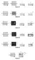
- FIGS. 1A-1Ishow plan- and cross-sectional views of a handle substrate and device substrate, respectively, illustrating a first embodiment of the present invention wherein:
- FIG. 1Ais a plan- and cross-sectional view of a handle-substrate and device substrate.
- FIG. 1Bis a plan- and cross-sectional view of a handle-substrate and device substrate after formation of a cavity.
- FIG. 1Cis a plan- and cross-sectional view of a handle-substrate and device substrate after formation of a trench and optional doping.
- FIG. 1Dis a plan- and cross-sectional view of a handle-substrate and device substrate after deposition or growth of an insulating dielectric material.
- FIG. 1Eis a plan- and cross-sectional view of a handle-substrate and device substrate after blanket etchback of the dielectric material from the device substrate.
- FIG. 1Fis a plan- and cross-sectional view of a handle-substrate and device substrate after bonding to form a bonded wafer pair
- FIG. 1Gis a plan- and cross-sectional view of a bonded wafer pair after removal of a portion of the device substrate showing an exposed isolation trench.
- FIG. 1His a plan- and cross-sectional view of a bonded wafer pair after optional processing that results in the formation of electrical interconnect.
- FIG. 1Iis a plan- and cross-sectional view of a bonded wafer pair after structural definition.
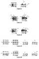
- FIGS. 2A-2Kare plan- and cross-sectional views of a handle substrate and device substrate illustrating a second embodiment of the invention wherein:
- FIG. 2Ais a plan- and cross-sectional view of a handle-substrate and device substrate.
- FIG. 2Bis a plan- and cross-sectional view of a handle-substrate and device substrate after formation of a trench.
- FIG. 2Cis a plan- and cross-sectional view of a handle-substrate and device substrate after deposition or growth of an insulating dielectric material.
- FIG. 2Dis a plan- and cross-sectional view of a handle-substrate and device substrate after patterning of the dielectric material into a hard-mask.
- FIG. 2Eis a plan- and cross-sectional view of a handle-substrate and device substrate after formation of a cavity.
- FIG. 2Fis a plan- and cross-sectional view of a handle-substrate and device substrate after blanket etchback of the remaining dielectric material from the device substrate.
- FIG. 2Gis a plan- and cross-sectional view of a handle-substrate and device substrate after an optional doping step.
- FIG. 2His a plan- and cross-sectional view of a handle-substrate and device substrate after bonding to form a bonded wafer pair
- FIG. 2Iis a plan- and cross-sectional view of a bonded wafer pair after removal of a portion of the device substrate showing an exposed isolation trench.
- FIG. 2Jis a plan- and cross-sectional view of a bonded wafer pair after optional processing that results in the formation of electrical interconnect.
- FIG. 2Kis a plan- and cross-sectional view of a bonded wafer pair after structural definition.
- FIGS. 3A-3Iare plan- and cross-sectional views of a handle substrate and device substrate illustrating a third embodiment of the invention wherein:
- FIG. 3Ais a plan- and cross-sectional view of a handle-substrate and device substrate.
- FIG. 3Bis a plan- and cross-sectional view of a handle-substrate and device substrate after formation of a trench.
- FIG. 3Cis a plan- and cross-sectional view of a handle-substrate and device substrate after an optional doping step.
- FIG. 3Dis a plan- and cross-sectional view of a handle-substrate and device substrate after deposition or growth of an insulating dielectric material.
- FIG. 3Eis a plan- and cross-sectional view of a handle-substrate and device substrate after blanket etchback of the dielectric material from the device substrate, and formation of a cavity in the handle substrate.
- FIG. 3Fis a plan- and cross-sectional view of a handle-substrate and device substrate after bonding to form a bonded wafer pair
- FIG. 3Gis a plan- and cross-sectional view of a bonded wafer pair after removal of a portion of the device substrate showing an exposed isolation trench.
- FIG. 3His a plan- and cross-sectional view of a bonded wafer pair after optional processing that results in the formation of electrical interconnect.
- FIG. 3Iis a plan- and cross-sectional view of a bonded wafer pair after structural definition.
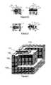
- FIG. 4is a perspective view of an electrically isolated structure with interconnection formed in accordance with the invention.
- FIG. 5is a perspective view of a single structural element comprised of two rigidly coupled masses with two distinct electrical nodes formed in accordance with the invention.
- FIG. 6is a plan- and cross-sectional view of a bonded wafer pair after structural definition with a trench-isolated region and a mechanical structure free from the handle wafer formed in the same device substrate in accordance with the invention.
- FIG. 7is a perspective cut-away view of one region in which stringers may form.
- FIG. 8Ais a plan-view and FIGS. 8 B,C are cross-sectional views of a trench with a condyle.
- FIG. 9Ais a plan-view and FIGS. 9 B,C are cross-sectional views of a trench with a condyle during deposition of insulating material and before pinching-off of the trench occurs.
- FIG. 10Ais a plan-view and FIGS. 10 B,C are cross-sectional views of a trench with a condyle during deposition of insulating material after pinching-off of the trench, but before pinching-off of the condyle occurs.
- FIG. 11Ais a plan-view and FIGS. 11 B,C are cross-sectional views of a trench with a condyle after deposition of insulating material and after pinching-off of both the trench and the condyle.
- FIGS. 12A-Fare a series of plan views of filled trenches with different-shaped filled condyles.
- FIG. 13is a plan view of a substantially planar device with multiple mechanical structures and multiple interconnects integrated with circuitry.
- FIG. 14is a plan view of a second substantially planar device with multiple mechanical structures and multiple interconnects integrated with circuitry.
- fabrication of a micromechanical device in accordance with the inventioncomprises six basic steps: providing a device substrate with first and second surfaces; providing a handle substrate with first and second surfaces; forming one or more filled isolation trenches portions of which lie within a recessed cavity on the first surface of the device substrate or alternatively forming one or more filled isolation trenches on the first surface of the device substrate and forming a recessed cavity on the first surface of the handle substrate; bonding the first surface of the device substrate to the first surface of the handle substrate; removing a portion of the second surface of the device substrate to expose at least one isolation trench; and etching a set of features in the second surface of the device substrate to complete the definition of electrically isolated structural elements.
- FIGS. 1 A through FIG. 1Iillustrate a first embodiment of the present invention. Both plan- and cross-sectional views of a portion of the device and handle substrates are shown to illustrate the steps in fabrication of devices in accordance with the present invention. Although only one mechanical device is shown for clarity throughout the following description, it will be understood that many mechanical structures are typically formed simultaneously on a single set of device and handle substrates.
- FIG. 1Ashows a handle substrate 100 and device substrate 101 , in plan view, and cross-sections A—A and B—B.
- the handle substrate 100may be a substantially homogenous material including, but not limited to: doped or undoped single-crystal silicon, quartz, glass, or aluminum oxide.
- the handle substratemay be a structure having a number of layers including: a thin layer of silicon dioxide on a first surface of silicon, and a thin layer of silicon nitride on a first surface of silicon.
- the device substrate 101may be single-crystal silicon, undoped silicon, p-type silicon, n-type silicon, silicon with a thin (5 to 50 microns) layer of heavily p-doped silicon on the first surface, and silicon with a thin layer (5 to 50 microns) of heavily ndoped silicon on the first surface.
- Both the handle and device substratesmay be substantially cylindrical wafers having a thickness of approximately 250 microns to 2 millimeters and a diameter from approximately 100 mm to 300 mm.
- a photolithographic mask(not shown) is used to form a first pattern in photosensitive material on a first face of the device substrate.
- the photosensitive materialmay be used to form a hard-mask pattern on the first surface of the device layer.
- a first etchdenoted the cavity etch, forms one or more cavities 102 in the first surface of the device substrate including at least one cavity that may be used for alignment of subsequent photolithography steps, the cavities being formed in regions where the device substrate is exposed through the first pattern.
- the cavity 102is typically 0.5 to 25 microns deep and may be etched using a plasma-etch, a wet anisotropic etch including potassium hydroxide (KOH), tetramethyl ammonium hydroxide (TMAH), ethylenediamine-pyrocatechol water (EDP), or an isotropic etch including a silicon etchant solution made from nitric acid, water, and ammonium fluoride.
- KOHpotassium hydroxide
- TMAHtetramethyl ammonium hydroxide
- EDPethylenediamine-pyrocatechol water
- an isotropic etchincluding a silicon etchant solution made from nitric acid, water, and ammonium fluoride.
- the first masking materialis removed, a photosensitive material is deposited on the first surface of the device substrate, a second photolithographic mask (not shown) is aligned to a feature formed during the cavity etch, and the photosensitive material patterned.
- the photosensitive materialmay be used to form a hard-mask pattern.
- a second etchforms one or more trenches 103 within a cavity 102 . At least one such trench may be used for alignment of subsequent photolithography steps.
- the trenchesare formed in regions where the device substrate is exposed through the second pattern.
- Trenches 103are typically 5 to 250 microns deep, 1 to 10 microns wide, and may be etched using a plasma-etch which may be a deep reactive-ion-etch, for example.
- the trenches 103may have a tapered profile as shown in FIG. 1C, or alternatively the trench may have substantially parallel sides.
- the trenchesmay have a tapered profile narrowing with depth, with sidewall angles less than approximately 20 degrees from the substantially parallel case.
- the second masking materialis removed.
- an optional doping stepmay be performed resulting in a layer of doped material 104 .
- the dopantmay include boron, phosphorous, antimony, arsenic or other species, and may be performed using solid-source diffusion, ion implantation, or liquid-dopants either spun-on or vapor-deposited. Solid-source and liquid-dopants allow the active species to be deposited along the sides of trenches 103 , potentially lowering structural interconnect resistance.
- the optional doping stepmay include a high-temperature drive-in step in which the dopant is diffused into the substrate.
- the insulating dielectricmay include, for example, deposited silicon dioxide, grown thermal oxide, deposited TEOS oxide, low-pressure chemical vapor deposited (LPCVD) silicon nitride, deposited phosphosilicate glass, deposited arsenic glass, deposited boron glass, or deposited boro-phosphosilicate glass.
- the insulating dielectricmay substantially fill the trenches 103 , or a separate material, such as polysilicon, may be subsequently deposited to substantially fill the trenches.
- the material deposited or grown during the previous stepmay be blanket-etched from the first surface of the covered device substrate, with the etch continuing until the first surface of the device substrate is exposed except at regions where trenches 103 exist, shown in FIG. 1 E.
- This etchalternatively referred to herein as a dielectric-removal etch, may be a plasma-etch or wet etch, with a composition appropriate for the chosen dielectric material 105 . Since this etch is a blanket-etch and ends when the substrate is exposed, dielectric material will remain in trenches 103 forming substantially filled isolation trenches 106 .
- a separate masking step in which a photolithographic mask is aligned to one or more features formed during either the cavity or trench etchesmay be used to protect selected areas of the deposited dielectric from removal at regions other than the trenches 103 .
- the first surface of the device substrate, or dielectricis bonded to the first surface of the handle substrate forming a bonded substrate pair 107 , as shown in FIG. 1 F.
- Bondingmay be attained by any of a number of well-known techniques including fusion bonding, thermal compression bonding, or anodic bonding.
- the bonding surfaces of the device- and handle-substratesmay be planarized to decrease defects in the device- to handle-substrate bond. Planarization may be achieved using, among other methods, chemical-mechanical polishing (CMP).
- CMPchemical-mechanical polishing
- the bonding processmay be carried out in a controlled atmosphere so that closed cavities 104 B are filled by a defined gas at a defined pressure.
- the bonding processmay be carried out in a partial vacuum, or in an atmosphere including nitrogen, argon, helium, oxygen, or hydrogen.
- device substrate materialis removed until the bottom 109 of at least one filled isolation trench 106 is exposed from a second surface of the device substrate that also forms a first surface 101 a of the bonded substrate pair 108 as shown in FIG. 1 G.
- removal of the substrate materialmay also expose filled isolation trenches that may be used for alignment of subsequent photolithography steps. Removal of material during this step may be achieved using many techniques known to those skilled in the art including: grinding, CMP, plasma-etching, and electrochemical etching. Note that if a particularly large micromechanical structure is to be formed, and thus a large cavity is required, studs may be created to help support the device layer in the presence of a differential pressure across the device layer.
- a differential pressuremay arise, for example, when the bonded substrate pair is placed in a low-pressure, high temperature chemical vapor deposition furnace and the cavity is filled with nitrogen.
- a studmay be formed by defining an annular or similar shaped cavity wherein the center of the annulus is incorporated into the bonding interface between the device and handle substrates. Large structures may be freed from studs by removing material surrounding the stud during the structural definition etch, described below.
- processingthat provides for electrical interconnect or circuitry, including transistors, may be carried out.
- Alignment of photolithographic masks used to define the interconnect or circuitry to the second surface of the device substratemay be achieved using the exposed trench bottoms 109 .
- the optional processingmay include the steps of: depositing or growing a first dielectric material 110 ; patterning the first dielectric material using photolithographic masks aligned to an alignment mark formed by one or more exposed trench bottoms 109 ; depositing a first layer of conducting material 111 ; patterning the first layer of conducting material; depositing a second dielectric layer 112 ; and patterning the second dielectric layer.
- the pattern formed in the first dielectric materialmay include one or more regions where electrical contacts 111 C to subsequently defined structural elements 116 are formed by the first layer of deposited conducting material.
- the optional processingmay include: alignment of a first photolithographic mask to an alignment mark formed by one or more exposed trench bottoms 109 ; implantation and diffusion of a doping material 113 ; depositing or growing a first dielectric material 110 ; patterning the first dielectric material 110 ; depositing a first layer of metal 111 ; patterning the first layer of metal; depositing a second dielectric layer 112 ; and patterning the second dielectric layer 112 .
- Circuit formationmay be accomplished using any number of well-known semiconductor circuit fabrication processes, including CMOS or BiCMOS, that will result in electronic circuit elements, such as transistors, and electrical interconnection among circuit elements. Circuit elements may be formed in regions remote from subsequently defined mechanical structures 116 . Circuit elements may also be formed in regions that are later defined into isolated mechanical structures 116 . Some of these structures may be movable with respect to the remainder of the device substrate. Note that the formation of mechanical structures mechanically free from the handle substrate without a wet release step renders etch holes unnecessary, enabling significant circuit complexity to be brought onto a mechanical structure. In addition, circuit formation may result in one or more conductors 111 that connect to the substrate material by contacts 111 C, shown in FIG. 1 H.
- the conductors and contactsmay permit electrical connection among subsequently defined structures 116 and electrical circuits.
- Electrical circuitsmay be used for measurement of capacitance (often called sense-capacitance) between isolated mechanical structures to yield a quantity representative of distance between the mechanical structures, for example. Electrical circuits may also be used to apply voltages to electrically isolated mechanical structures to generate electrostatic forces. Other uses of electrical circuits include, but are not limited to: calculating or signal processing of quantities based on measurements of sense-capacitance; sustaining oscillation of a mechanical structure; measurement of changes in a piezoresistor which may be formed in the device substrate; and measurement of current flow due to electron-tunneling between isolated mechanical structures.
- One or more mechanical structures 116are defined with a third etch, alternatively referred to herein as a structure-definition etch.
- an anisotropic etchwhich may, for example, be a deep reactive-ion-etch, removes portions of device substrate 101 to expose and open at least one closed cavity 104 B. Removal of excess material of substrate 101 leaves open regions 115 that define at least one mechanical structure 116 .
- Structural elementsmay include but are not limited to, one or more beams, flexures, springs, levers, proof-masses, fixed air-gap capacitors, and variable air-gap capacitors. The removal of excess material of substrate 101 not only defines mechanical structures but also provides a majority of required electrical isolation between isolated mechanical structures. Additional isolation is provided by isolation trenches 106 .
- a perspective view of a simple cantilever beam with electrical isolation and interconnection formed in accordance with the present inventionis shown in FIG. 4 .
- the specific order in which certain steps occurmay be interchanged, or the substrate in which the cavity is formed may be varied.
- a first variationis shown in FIG. 2 A through FIG. 2K in accordance with a second embodiment of the method according to the invention.
- the method according to the inventionis comprised of the same six basic steps as the first embodiment, with a variation in the means by which the filled isolation trenches within a recessed cavity on the first surface of the device substrate are formed.
- a photolithographic mask(not shown) is used to form a first pattern in photosensitive material on a first face of the device substrate 201 .
- the photosensitive materialmay be used to form a hard-mask pattern on the first surface of the device layer.
- a trench etchforms one or more trenches 203 in the first surface of the device substrate including at least one trench that may be used for alignment of subsequent photolithography steps, the trenches being formed in regions where the device substrate is exposed through the first pattern.
- Trenches 203are typically 5 to 250 microns deep, 1 to 10 microns wide, and may be etched using a plasma-etch which may be a deep reactive-ion-etch, for example.
- the trenches 203may have a tapered profile as shown in FIG. 2B, or alternatively the trench may have substantially parallel sides.
- the trenchesmay have a tapered profile narrowing with depth, the profile having sidewall angles less than approximately 20 degrees from the substantially parallel case.
- an insulating dielectric 205is deposited or grown on the device substrate as illustrated in FIG. 2 C.
- the insulating dielectricmay include deposited silicon dioxide, grown wet thermal oxide, grown dry thermal oxide, deposited TEOS oxide, LPCVD silicon nitride, deposited phosphosilicate glass, deposited arsenic glass, deposited boron glass, or deposited boro-phosphosilicate glass.
- the insulating dielectricmay substantially fill the trenches 203 , or a separate material, such as polysilicon, may be subsequently deposited to substantially fill the trenches.
- dielectric 205 deposited or grown during the previous stepmay be photolithographically patterned, with a mask aligned to one or more filled isolation trenches, and etched from the first surface of the covered device substrate. The etch continues until the first surface of the device substrate is exposed in areas defined by openings in the mask, FIG. 2 D.
- This etchalternatively referred to herein as the dielectricremoval etch, may be a plasma-etch or wet etch, with a composition appropriate for the chosen dielectric material 205 . Patterning the dielectric material 205 in this fashion results in a hard-mask that may be used in the subsequent cavity-etch step.
- the material deposited or grown during the previous stepmay be blanket-etched from the first surface of the covered device substrate, with the etch continuing until the first surface of the device substrate is exposed except at regions where trenches 203 exist.
- a separate photolithography step with a photosensitive material, aligned to one or more filled isolation trenches,is performed to define areas in which subsequent cavities are to be etched. Note that in both cases the blanket-etch ends when the substrate is exposed; thus, dielectric material will remain in trenches 203 forming substantially filled isolation trenches 206 .
- a cavity etchsubsequently forms one or more cavities 202 in the first surface of the device substrate, the cavities being formed in regions where the device substrate is exposed through the hard-mask pattern or the pattern formed by the photosensitive material.
- the cavity 202is typically 0.5 to 25 microns deep and may be etched using a plasma-etch, a wet anisotropic etch including potassium hydroxide, TMAH, or EDP, or an isotropic etch including a silicon etchant solution made from nitric acid, water, and ammonium fluoride.
- TMAHpotassium hydroxide
- EDPan isotropic etch including a silicon etchant solution made from nitric acid, water, and ammonium fluoride.
- An optional doping stepmay now be performed resulting in a layer of doped material 204 , shown in FIG. 2 G.
- the dopantmay include boron, phosphorous, antimony, arsenic or other species and may be deposited using solid-source diffusion, ion implantation, or liquid-dopants either spun-on or vapor-deposited.
- the optional doping stepmay include a high-temperature drive-in step in which the dopant is diffused into the substrate.
- the first surface of the device substrate, or dielectric if not removed from the first surface of the device substrate,may be bonded to the first surface of the handle substrate 200 forming a bonded substrate pair 207 , as shown in FIG. 2 H.
- Bondingmay be attained by any of a number of well-known techniques including fusion bonding, thermal compression bonding, or anodic bonding.
- the bonding surfaces of the device- and handle-substratesmay be planarized to decrease defects in the device- to handle-substrate bond. Planarization may be achieved using, among other methods, chemical-mechanical polishing.
- the bonding processmay be carried out in a controlled atmosphere so that closed cavities 204 B are filled by a defined gas at a defined pressure.
- the bonding processmay be carried out in a partial vacuum, or in an atmosphere including nitrogen, argon, or helium, oxygen, or hydrogen.
- materialis removed until the bottom 209 of at least one filled isolation trench 206 is exposed from a second surface of the device substrate that also forms a first surface of the bonded substrate pair 208 as shown in FIG. 2 I.
- removal of the substrate materialmay also expose filled isolation trenches that may be used for alignment of subsequent photolithography steps. Removal of material during this step may be achieved using many techniques known to those skilled in the art including: grinding, chemical-mechanical polishing, plasma-etching, and electrochemical etching.
- optional processingthat provides for electrical interconnect or circuitry, including transistors, may be carried out, as described in the first embodiment and shown in FIG. 2 J. Structures are subsequently defined as described in the first embodiment and shown in FIG. 2 K.
- FIG. 3 A through FIG. 3IA second variation of the method according to the invention is shown in FIG. 3 A through FIG. 3I in a third embodiment.
- the method according to the inventionis comprised of the same six basic steps as the first embodiment, with a variation in which substrate the cavities are formed; specifically, cavities are formed in the first surface of the handle substrate.
- a photolithographic mask(not shown) is used to form a first pattern in photosensitive material on a first face of the device substrate.
- the photosensitive materialmay be used to form a hard-mask pattern on the first surface of the device layer.
- a trench etchforms one or more trenches 303 in the first surface of the device substrate 301 including at least one trench that may be used for alignment of subsequent photolithography steps, the trenches being formed in regions where the device substrate is exposed through the first pattern.
- Trenches 303are typically 5 to 250 microns deep, 1 to 10 microns wide, and may be etched using a plasma-etch which may be a deep reactive-ion-etch, for example.
- the trenches 303may have a tapered profile as shown in FIG. 3 b, or alternatively the trench may have substantially parallel sides.
- the trenchesmay have a tapered profile narrowing with depth, the profile having sidewall angles less than approximately 20 degrees from the substantially parallel case.
- An optional doping stepmay now be performed resulting in a layer of doped material 304 , shown in FIG. 3 C.
- the dopantmay include boron, phosphorous, antimony, arsenic or other species and may be deposited using solid-source diffusion, ion implantation, or liquid-dopants either spun-on or vapor-deposited.
- the optional doping stepmay include a high-temperature drive-in step in which the dopant is diffused into the substrate.
- the insulating dielectric 305is deposited or grown on the device substrate as illustrated in FIG. 3 D.
- the insulating dielectric 305may include deposited silicon dioxide, grown wet thermal oxide, grown dry thermal oxide, deposited TEOS oxide, LPCVD silicon nitride, deposited phosphosilicate glass, deposited arsenic glass, deposited boron glass, or deposited boro-phosphosilicate glass.
- the insulating dielectricmay substantially fill the trenches 303 , or a separate material, such as polysilicon, may be subsequently deposited to substantially fill the trenches.
- the insulating dielectric 305 deposited or grown during the previous stepmay be blanket-etched from the first surface of the covered device substrate, with the etch continuing until the first surface of the device substrate is exposed except at regions where trenches 303 exist.
- This etchalternatively referred to as the dielectric-removal etch, may be a plasma-etch or wet etch, with a composition appropriate for the chosen dielectric material 305 . Since the blanket-etch ends when the substrate is exposed, dielectric material will remain in trenches 303 forming substantially filled isolation trenches 306 .
- a separate masking step in which a photolithographic mask is aligned to one or more features formed during the trench etchmay be used to protect selected areas of the deposited dielectric from removal at regions other than the trenches 303 .
- a cavity etchforms one or more cavities 302 in the first surface of the handle substrate, the cavities being formed in regions where the handle substrate is exposed through a hard-mask, formed by a photolithography and etch step to form a hard-mask pattern, or a pattern formed by a photolithography step.
- the cavity 302is typically 0.5 to 25 microns deep and may be etched using a plasma-etch, a wet anisotropic etch including potassium hydroxide, TMAH, or EDP, or an isotropic etch including a silicon etchant solution made from nitric acid, water, and ammonium fluoride.
- TMAHpotassium hydroxide
- EDPan isotropic etch including a silicon etchant solution made from nitric acid, water, and ammonium fluoride.
- the first surface of the device substrate 301may be aligned and bonded to the first surface of the handle substrate 300 forming a bonded substrate pair 307 , as shown in FIG. 3 F.
- Alignment of the filled trenches 306 to the cavities 302may be provided by an optical alignment system that uses infrared light to make the relative positions of filled trenches 306 and cavities 302 known.
- an aligner that uses visible light for wafer to wafer alignmentmay be used, such as the Karl Suss Bond Aligner (MA/BA6). Bonding may be attained by any of a number of well known techniques including fusion bonding, thermal compression bonding, or anodic bonding.
- the bonding surfaces of the device- and handle-substratesmay be planarized to decrease defects in the device- to handle-substrate bond. Planarization may be achieved using, among other methods, chemical-mechanical polishing.
- the bonding processmay be carried out in a controlled atmosphere so that closed cavities 304 B are filled by a defined gas at a defined pressure.
- the bonding processmay be carried out in a partial vacuum, or in an atmosphere including nitrogen, argon, or helium, oxygen, or hydrogen.
- materialis removed until the bottom 309 of at least one filled isolation trench 306 is exposed from a second surface of the device substrate that also forms a first surface of the bonded substrate pair 308 as shown in FIG. 3 G.
- removal of the substrate materialmay also expose filled isolation trenches that may be used for alignment of subsequent photolithography steps. Removal of material during this step may be achieved using many techniques known to those skilled in the art including: grinding, chemical-mechanical polishing, plasma-etching, and electrochemical etching.
- optional processing that provides for electrical interconnect or circuitry, including transistorsmay be carried out, as described in the first embodiment and shown in FIG. 3 H. Structures are subsequently defined as described in the first embodiment and shown in FIG. 3 I.
- FIG. 5shows an example of a single structural element that contains two masses 116 a,b rigidly joined by a trench 106 c, the structural element having two distinct electrical nodes.
- structural nodesmay be electrically isolated from one another by such refilled trenches 106 c.
- the structureis electrically isolated from and mechanically anchored to the device substrate by refilled trench 106 a. Electrical interconnection to the different masses is made using conductive interconnect 111 f,g in conjunction with electrical contacts 111 d,e.
- Note refilled trench 106 cis not mechanically attached to the underlying handle substrate due to the nature of the process sequence, thereby enabling movement of released mechanical structures with respect to the substrate.
- the method described abovealso provides for formation of structural elements in the same device substrate as electrically isolated regions that are firmly attached to the handle substrate. Isolation of regions of the device substrate attached to the handle substrate may be provided for when the device 201 a and handle substrates 200 a are bonded with a layer of insulating dielectric 205 b between or part of at least one of the substrates, and filled trenches 206 b are formed outside regions where a cavity is etched into the first surface of the device substrate during the cavity etch. For example, referring to FIG.
- the isolated regions 201 bare laterally isolated from the remainder of the device substrate 201 a by a filled isolation trench 206 b, and are vertically isolated from the handle substrate 200 a by the layer of the deposited or grown dielectric material 205 b. Note the method provides for simultaneous formation of electrically isolated mechanical structures 216 a with isolation trenches 206 c that are mechanically free from the underlying handle substrate.
- Co-location of mechanical structures that are free from the handle substrate on the same device substrate as electrically isolated regions attached to the handle substratemay be advantageous in cases when it is desirable to have particular regions of circuitry isolated from one another, including: mixed signal circuits with an analog and a digital component; there are sensitive portions of an analog circuit, for example a voltage reference; isolation of the collector from the substrate in a bipolar transistor formed in a CMOS circuit technology; and decoupling of circuit power and ground, allowing for the use of two or more independent power supplies.
- One method by which electrical conduction may occuris through conductive “stringers” 428 (FIG. 7) located along the wall of the isolation trench.
- a stringeris defined as undesirable material left behind after etching.
- An example of a stringeris shown in FIG. 7 .
- Use of a tapered trench profile such as shown in FIG. 1Cmay help minimize stringer formation.
- Further elimination of stringersmay be provided by ensuring isolation trenches extend into a region cleared during the structural-definition etch at each point where isolation is desired. A protrusion of a trench into such a region is termed a “nubbin” 423 .
- every isolation trench 106 , 206 , 306terminates in a region 115 , 215 , 315 cleared during the structural-definition etch (i.e. every trench ends with a nubbin)
- three faces of the trenchare exposed to the etch.
- Increased exposure to the structural-definition etchreduces incidence of stringers and results improved isolation characteristics of the device.
- trench fill materials attacked by the second deep etchmay be selected, including silicon nitride and silicon dioxide, resulting in etching of the nubbins 423 .
- trenches 103may have keyholes 427 after filling.
- a keyholeis produced when the trench-fill material plugs the exposed entrance to a trench before enough material may be deposited to completely fill the center region of the trench. Keyhole formation is undesirable because keyholes may significantly reduce the mechanical strength and reliability of the trench.
- Use of a tapered trench profile such as shown in FIG. 1Cmay help minimize keyhole formation.
- the trench-fill depositionis substantially isotropic (such as LPCVD silicon nitride or TEOS silicon dioxide) keyhole formation may be further reduced using condyles, which are areas along the length of the filled trenches with an increased width.
- FIG. 8A, 8 B-Cshow plan and cross-sectional views of a trench 403 a and a condyle 403 b before dielectric insulating material 405 is deposited.
- FIG. 9shows the formation of lips 429 at the top of the trench which eventually pinch-off the trench entrance as shown in FIG. 10 . Once the lips pinch-off further deposition of material inside the trench from the top is prevented. Since the cross-sectional area of the condyle is greater than the cross sectional area of the trench the condyle enables further deposition of material by lateral migration until the lips at the top of the condyle pinch-off, shown in FIG. 11 .
- filled condyles 424 a-f attached to filled trenches 406are shown in FIG. 12A-F.
- small regions of a trenchmay be chosen to have an increased width.
- condylesmay be formed at one or both ends of a trench, along the length of a trench including one or more ends, or along the length of a trench not including the ends, as illustrated in FIG. 12A-F.
- Condyle shapesare not limited to the examples shown, many shapes with an effective cross-sectional width greater than the nominal trench width may serve as a condyle.
- FIG. 13illustrates an accelerometer that measures translational acceleration along an input axis.
- the principles of the inventionare applicable to many other devices including, but not limited to: gyroscopes; angular accelerometers; mechanical filters; resonators or oscillators; mechanical valves; actuators, such as disk-drive head actuators; and passive mechanical structures such as gimbals.
- the illustrated accelerometer built in device substrate 101 aincludes a proof-mass 116 c, stationary interdigitated comb fingers 116 f,g CMOS electronic circuitry 125 a, and electrical interconnect 111 h,i,j. Electrical contact from the interconnect to the mechanical structures are made with contacts 111 k, which are, in this example, substrate contacts formed during CMOS circuit processing.
- the proof-mass 116 cis defined by removal of regions of excess device substrate material 101 a leaving open area 115 b.
- the proof-massincludes a flexure 116 d that allows the proofmass to deflect, and comb-fingers 116 e that are interleaved with stationary comb-fingers 116 f,g.
- Proof-mass comb-fingers 116 eform the center node of a capacitive half-bridge with stationary comb-fingers 116 f,g. Deflections of the proof-mass from translational accelerations along the input axis result in an imbalance in the half-bridge.
- Electronic circuitry 125 amay measure this imbalance to infer acceleration. Furthermore, electronic circuitry 125 a may force-balance the proof-mass using electrostatic attraction between comb-fingers 116 e and 116 f,g or one or more separate sets of comb-fingers.
- FIG. 14illustrates an accelerometer that measures translational acceleration having a single isolation trench 106 f.
- the illustrated accelerometer built in device substrate 101 bincludes a proof-mass 116 h, stationary interdigitated comb fingers 116 k,m CMOS electronic circuitry 125 b, and a first layer of conductive electrical interconnect 111 m,n,o. Electrical contact from the first layer of interconnect to the mechanical structures are made with contacts 111 p, which are, in this example, substrate contacts formed during CMOS circuit processing.
- contacts 111 pwhich are, in this example, substrate contacts formed during CMOS circuit processing.
- a second layer of conductive interconnect 121 amay be used for routing of electrical signals and is connected to the first layer of conductive interconnect by contacts 111 q.
- the proof-mass 116 his defined by removal of regions of excess device substrate material 101 b leaving open area 115 c.
- the proof-massincludes a flexure 116 i that allows the proof-mass to deflect, and comb-fingers 116 j that are interleaved with stationary comb-fingers 116 k,m.
- Proof-mass comb-fingers 116 jform the center node of a capacitive half-bridge with stationary comb-fingers 116 k,m. Deflections of the proof-mass from translational accelerations along the input axis result in an imbalance in the half-bridge.
- Electronic circuitry 125 bmay measure this imbalance to infer acceleration.
- electronic circuitry 125 bmay force-balance the proof-mass using electrostatic attraction between comb-fingers 116 j and 116 k,m or one or more separate sets of comb-fingers.
- Many of the mechanical elementssuch as the proof-mass and the stationary, interdigitated comb-fingers are electrically isolated from each other, the circuitry, and the remainder of the substrate by a combination of regions 115 c formed during the structural definition etch, and a filled isolation trench 106 f that encloses a region in which mechanical structures are defined.
- Optional condylesmay be added for improved trench filling.
- Accelerometer performanceis enhanced over prior-art implementations due to the high-aspect-ratio fabrication that yields larger mass, air-gap capacitors with larger sensitivity, and improved suppression of undesired deflections out of the plane of the device substrate.
- Fabrication of accelerometers in accordance with the inventionprovides mechanical structures mechanically free from the handle substrate without a wet release step, increasing yield and decreasing processing complexity.
- Fabrication of accelerometers in accordance with the inventionprovides for substantially voidless isolation trench fill while maintaining good electrical isolation across isolation trenches. Isolation may be enhanced when the trenches use either nubbins or a tapered trench profile as shown in FIG. 1 C.
- a trenchmay extend through the device substrate such that only a portion of the trench is disposed above a cavity; trenches may be various shapes, including a U, for example; and trenches may include curves or bends as viewed from perspective view.
- the embodimentswere chosen and described in order to best explain the principles of the invention and its practical applications, to thereby enable others skilled in the art to best utilize the invention and various embodiments with various modifications as are suited to the particular use contemplated.
Landscapes
- Engineering & Computer Science (AREA)
- Power Engineering (AREA)
- Physics & Mathematics (AREA)
- General Physics & Mathematics (AREA)
- Microelectronics & Electronic Packaging (AREA)
- Manufacturing & Machinery (AREA)
- Micromachines (AREA)
- Element Separation (AREA)
Abstract
Description
This application claims priority to Provisional Application Serial No. 60/127,973 filed Apr. 6, 1999 entitled “MICROFABRICATED STRUCTURES WITH TRENCH-ISOLATION USING BONDED-SUBSTRATES AND CAVITIES.”
1. Field of the Invention
This invention relates generally to microfabricated devices, and more particularly to three-dimensional devices fabricated with high vertical to horizontal aspect ratios. This invention results in high-aspect-ratio devices that may be fabricated with integrated circuitry on the same substrate using conventional microfabrication techniques.
2. Description of the Related Art
MicroElectroMechanical Systems (MEMS) combine mechanical structures and microelectronic circuits to create devices. MEMS have many useful applications such as microsensors and microactuators. Examples of microsensors include inertial instruments such as accelerometers and gyroscopes, detectors for gasses such as carbon-monoxide, and pressure sensors. Examples of microactuators include optical mirrors used for video displays and disk-drive head actuators used for increasing track density. Passive mechanical structures may also be fabricated in a MEMS technology such as a gimbal for a disk-drive head actuator.
Many MEMS-based devices utilize electrical circuits combined with air-gap capacitors to sense motion, or to apply electrostatic forces to a movable structure. Air-gap capacitors are often formed between sets of capacitor plates anchored to a substrate interleaved with plates attached to a movable structure. The performance of many capacitive-based MEMS improves as: 1) the overlap area of capacitor plates increases, 2) the distance between the stationary and movable capacitor plates decreases, 3) the compliance of the structure varies dramatically in different directions, 4) the mass of the structure increases, and 5) the ratio of parasitic capacitance to active sense capacitance decreases. Each of these performance issues is enhanced using high-aspect-ratio semiconductor technologies, wherein thickness or depth of fabricated structures is much larger than small lateral dimensions such as width of flexible beams and gaps between capacitor plates.
Electrical interfaces for capacitive-based MEMS require electrically isolated nodes spanned by one or more variable capacitors such as an air-gap capacitor. Thus, capacitive interfaces using capacitors formed between structural elements require electrical isolation between these structural elements when the structural elements are formed out of a single conductive substrate.
The performance of devices such as accelerometers and gyroscopes may benefit from combining high-aspect-ratio structures with circuits integrated in the same substrate. Hence, a high-aspect-ratio structure etched into a single-crystal silicon substrate that also contains integrated circuits is of particular interest. Of even greater interest is a process sequence that yields structures and circuits in the same substrate but does not significantly alter complex and expensive circuit fabrication processes. Such a process sequence enables cost-effective manufacture of devices comprising integrated circuits and structures on a single substrate.
For improved performance, an integrated MEMS process should address three issues. First, the structural elements should be formed by a high-aspect-ratio process. Second, fabrication of mechanical structures should have a minimal impact on fabrication of associated circuitry on the same substrate. Third, structural elements should be electrically isolated from one another, the substrate, and circuit elements except where interconnection is desired.
The invention, roughly described, comprises a microelectromechanical structure and method of forming the structure. In one aspect, the method includes: providing a handle substrate; providing a device substrate in which high-aspect-ratio structures and optional integrated circuitry will be fabricated; forming one or more filled isolation trenches within a recessed cavity on a first surface of the device substrate or alternatively forming one or more filled isolation trenches on a first surface of the device substrate and forming a recessed cavity on a first surface of the handle substrate; bonding the first surface of the device substrate to the handle substrate; removing a substantially uniform amount of material from the second surface of the device substrate to expose at least one isolation trench; optionally forming circuits and interconnection on a second surface of the device substrate; and etching a set of features in the second surface of the device substrate to complete the definition of electrically isolated structural elements. The structural-definition etch may also provide electrical isolation among various structural elements, and provide electrical isolation between structural elements and the device substrate except at mechanical attachment points between structural elements or structural elements and the device substrate. The isolation trenches and an insulating material deposited in the isolation trenches may provide electrical isolation at these mechanical attachment points. Structural elements may include, but are not limited to one or more of the following: beams, flexures, springs, levers, proof-masses, fixed air-gap capacitors, and variable air-gap capacitors.
In a further aspect of the invention, a device includes: a device substrate having a first surface, a second surface, and a semiconductor layer; a handle substrate, the first surface of the device substrate bonded to the handle substrate; one or more first trenches formed in the device substrate, the first trenches extending from the second surface of the device substrate through the device substrate towards the handle substrate; a dielectric within the first trenches; one or more cavities disposed below the second surface of the device layer, a cavity enclosing a portion of at least one trench; at least one second trench formed in the second surface of the device substrate, the second trench completing definition of one or more micromechanical devices. The second trench may provide electrical isolation among various structural elements, and provide electrical isolation between structural elements and the device substrate except at mechanical attachment points between structural elements or structural elements and the device substrate. The first trenches provide electrical isolation at these mechanical attachment points. Micromechanical elements may include, but are not limited to one or more of the following: beams, flexures, springs, levers, proof-masses, fixed air-gap capacitors, and variable air-gap capacitors.
The invention allows conducting material to be deposited over exposed isolating trenches to provide electrical connectivity to the structural elements. Conducting material deposited over exposed isolating trenches may also be used to interconnect among electrically isolated circuit and structural elements. Circuit elements may be formed in the device substrate including active devices such as transistors. A single insulating material deposited or grown in the trenches may entirely fill the trenches or an additional filler material may be added to complete filling of trenches after an initial deposition of a first insulating material. The handle or device substrate may include single-crystal or epitaxial silicon, the isolation material may include silicon dioxide or silicon nitride, and the trench fill material may include polycrystalline silicon.
Advantages of the invention include improving the performance of microstructures fabricated in accordance with the invention due to the high-aspect-ratio fabrication that yields larger mass, air-gap capacitors with larger sensitivity, and improved suppression of undesired deflections particularly deflections out of the plane of the device substrate. Fabrication of devices in accordance with the invention may provide mechanical structures mechanically free from the handle substrate without a wet release step. Fabrication of devices in accordance with the invention may also provide a means for alignment of photolithographic masks to a nominally hidden recessed cavity, enabling accurate placement of mechanical structures and optional interconnect or circuits with respect to the recessed cavity with standard photolithographic tools. Fabrication of devices in accordance with the invention may provide substantially voidless isolation trench fill while maintaining good electrical isolation across isolation trenches. Fabrication of devices in accordance with the invention may furthermore provide lower parasitic capacitances in proportion to active sense capacitance than prior art inventions since the invention allows for the use of lower dielectric constant isolation materials than prior art solutions. When circuits are co-fabricated on the device substrate with the mechanical device, performance of devices fabricated in accordance with the invention may be improved due to the proximity of interface circuitry built into the same substrate as the microstructure. Furthermore, when circuits are co-fabricated on the device substrate with the mechanical device, the handle substrate is comprised of heavily doped silicon, the device substrate is comprised of silicon, and the two substrates are bonded by either fusion or thermal compression bonding, a low resistance contact to the back-side of the circuits may be attained.
The invention will be described with respect to the particular embodiments thereof. Other objects, features, and advantages of the invention will become apparent with reference to the specification and drawings in which:
FIGS. 1A-1I show plan- and cross-sectional views of a handle substrate and device substrate, respectively, illustrating a first embodiment of the present invention wherein:
FIG. 1A is a plan- and cross-sectional view of a handle-substrate and device substrate.
FIG. 1B is a plan- and cross-sectional view of a handle-substrate and device substrate after formation of a cavity.
FIG. 1C is a plan- and cross-sectional view of a handle-substrate and device substrate after formation of a trench and optional doping.
FIG. 1D is a plan- and cross-sectional view of a handle-substrate and device substrate after deposition or growth of an insulating dielectric material.
FIG. 1E is a plan- and cross-sectional view of a handle-substrate and device substrate after blanket etchback of the dielectric material from the device substrate.
FIG. 1F is a plan- and cross-sectional view of a handle-substrate and device substrate after bonding to form a bonded wafer pair
FIG. 1G is a plan- and cross-sectional view of a bonded wafer pair after removal of a portion of the device substrate showing an exposed isolation trench.
FIG. 1H is a plan- and cross-sectional view of a bonded wafer pair after optional processing that results in the formation of electrical interconnect.
FIG. 1I is a plan- and cross-sectional view of a bonded wafer pair after structural definition.
FIGS. 2A-2K are plan- and cross-sectional views of a handle substrate and device substrate illustrating a second embodiment of the invention wherein:
FIG. 2A is a plan- and cross-sectional view of a handle-substrate and device substrate.
FIG. 2B is a plan- and cross-sectional view of a handle-substrate and device substrate after formation of a trench.
FIG. 2C is a plan- and cross-sectional view of a handle-substrate and device substrate after deposition or growth of an insulating dielectric material.
FIG. 2D is a plan- and cross-sectional view of a handle-substrate and device substrate after patterning of the dielectric material into a hard-mask.
FIG. 2E is a plan- and cross-sectional view of a handle-substrate and device substrate after formation of a cavity.
FIG. 2F is a plan- and cross-sectional view of a handle-substrate and device substrate after blanket etchback of the remaining dielectric material from the device substrate.
FIG. 2G is a plan- and cross-sectional view of a handle-substrate and device substrate after an optional doping step.
FIG. 2H is a plan- and cross-sectional view of a handle-substrate and device substrate after bonding to form a bonded wafer pair
FIG. 2I is a plan- and cross-sectional view of a bonded wafer pair after removal of a portion of the device substrate showing an exposed isolation trench.
FIG. 2J is a plan- and cross-sectional view of a bonded wafer pair after optional processing that results in the formation of electrical interconnect.
FIG. 2K is a plan- and cross-sectional view of a bonded wafer pair after structural definition.
FIGS. 3A-3I are plan- and cross-sectional views of a handle substrate and device substrate illustrating a third embodiment of the invention wherein:
FIG. 3A is a plan- and cross-sectional view of a handle-substrate and device substrate.
FIG. 3B is a plan- and cross-sectional view of a handle-substrate and device substrate after formation of a trench.
FIG. 3C is a plan- and cross-sectional view of a handle-substrate and device substrate after an optional doping step.
FIG. 3D is a plan- and cross-sectional view of a handle-substrate and device substrate after deposition or growth of an insulating dielectric material.
FIG. 3E is a plan- and cross-sectional view of a handle-substrate and device substrate after blanket etchback of the dielectric material from the device substrate, and formation of a cavity in the handle substrate.
FIG. 3F is a plan- and cross-sectional view of a handle-substrate and device substrate after bonding to form a bonded wafer pair
FIG. 3G is a plan- and cross-sectional view of a bonded wafer pair after removal of a portion of the device substrate showing an exposed isolation trench.
FIG. 3H is a plan- and cross-sectional view of a bonded wafer pair after optional processing that results in the formation of electrical interconnect.
FIG. 3I is a plan- and cross-sectional view of a bonded wafer pair after structural definition.
FIG. 4 is a perspective view of an electrically isolated structure with interconnection formed in accordance with the invention.
FIG. 5 is a perspective view of a single structural element comprised of two rigidly coupled masses with two distinct electrical nodes formed in accordance with the invention.
FIG. 6 is a plan- and cross-sectional view of a bonded wafer pair after structural definition with a trench-isolated region and a mechanical structure free from the handle wafer formed in the same device substrate in accordance with the invention.
FIG. 7 is a perspective cut-away view of one region in which stringers may form.
FIG. 8A is a plan-view and FIGS.8B,C are cross-sectional views of a trench with a condyle.
FIG. 9A is a plan-view and FIGS.9B,C are cross-sectional views of a trench with a condyle during deposition of insulating material and before pinching-off of the trench occurs.
FIG. 10A is a plan-view and FIGS.10B,C are cross-sectional views of a trench with a condyle during deposition of insulating material after pinching-off of the trench, but before pinching-off of the condyle occurs.
FIG. 11A is a plan-view and FIGS.11B,C are cross-sectional views of a trench with a condyle after deposition of insulating material and after pinching-off of both the trench and the condyle.
FIGS. 12A-F are a series of plan views of filled trenches with different-shaped filled condyles.
FIG. 13 is a plan view of a substantially planar device with multiple mechanical structures and multiple interconnects integrated with circuitry.
FIG. 14 is a plan view of a second substantially planar device with multiple mechanical structures and multiple interconnects integrated with circuitry.
In general, fabrication of a micromechanical device in accordance with the invention comprises six basic steps: providing a device substrate with first and second surfaces; providing a handle substrate with first and second surfaces; forming one or more filled isolation trenches portions of which lie within a recessed cavity on the first surface of the device substrate or alternatively forming one or more filled isolation trenches on the first surface of the device substrate and forming a recessed cavity on the first surface of the handle substrate; bonding the first surface of the device substrate to the first surface of the handle substrate; removing a portion of the second surface of the device substrate to expose at least one isolation trench; and etching a set of features in the second surface of the device substrate to complete the definition of electrically isolated structural elements.
FIGS.1A through FIG. 1I illustrate a first embodiment of the present invention. Both plan- and cross-sectional views of a portion of the device and handle substrates are shown to illustrate the steps in fabrication of devices in accordance with the present invention. Although only one mechanical device is shown for clarity throughout the following description, it will be understood that many mechanical structures are typically formed simultaneously on a single set of device and handle substrates.
FIG. 1A shows ahandle substrate 100 anddevice substrate 101, in plan view, and cross-sections A—A and B—B. For convenience, FIGS. 1B-1I use common nomenclature and reference numbers. While different materials may be used, thehandle substrate 100 may be a substantially homogenous material including, but not limited to: doped or undoped single-crystal silicon, quartz, glass, or aluminum oxide. Alternatively the handle substrate may be a structure having a number of layers including: a thin layer of silicon dioxide on a first surface of silicon, and a thin layer of silicon nitride on a first surface of silicon. Thedevice substrate 101 may be single-crystal silicon, undoped silicon, p-type silicon, n-type silicon, silicon with a thin (5 to 50 microns) layer of heavily p-doped silicon on the first surface, and silicon with a thin layer (5 to 50 microns) of heavily ndoped silicon on the first surface. Both the handle and device substrates may be substantially cylindrical wafers having a thickness of approximately 250 microns to 2 millimeters and a diameter from approximately 100 mm to 300 mm.
In FIG. 1B, a photolithographic mask (not shown) is used to form a first pattern in photosensitive material on a first face of the device substrate. Alternatively, in conjunction with an appropriate deposited or grown masking material such as silicon dioxide, the photosensitive material may be used to form a hard-mask pattern on the first surface of the device layer. A first etch, denoted the cavity etch, forms one ormore cavities 102 in the first surface of the device substrate including at least one cavity that may be used for alignment of subsequent photolithography steps, the cavities being formed in regions where the device substrate is exposed through the first pattern. Thecavity 102 is typically 0.5 to 25 microns deep and may be etched using a plasma-etch, a wet anisotropic etch including potassium hydroxide (KOH), tetramethyl ammonium hydroxide (TMAH), ethylenediamine-pyrocatechol water (EDP), or an isotropic etch including a silicon etchant solution made from nitric acid, water, and ammonium fluoride.
Next, the first masking material is removed, a photosensitive material is deposited on the first surface of the device substrate, a second photolithographic mask (not shown) is aligned to a feature formed during the cavity etch, and the photosensitive material patterned. Again, alternatively the photosensitive material may be used to form a hard-mask pattern.
As shown in FIG. 1C, a second etch, alternatively referred to herein as the trench etch, forms one ormore trenches 103 within acavity 102. At least one such trench may be used for alignment of subsequent photolithography steps. The trenches are formed in regions where the device substrate is exposed through the second pattern.Trenches 103 are typically 5 to 250 microns deep, 1 to 10 microns wide, and may be etched using a plasma-etch which may be a deep reactive-ion-etch, for example. Thetrenches 103 may have a tapered profile as shown in FIG. 1C, or alternatively the trench may have substantially parallel sides. The trenches may have a tapered profile narrowing with depth, with sidewall angles less than approximately 20 degrees from the substantially parallel case. Next, the second masking material is removed.
At this point an optional doping step may be performed resulting in a layer of dopedmaterial 104. If the doping step is performed the dopant may include boron, phosphorous, antimony, arsenic or other species, and may be performed using solid-source diffusion, ion implantation, or liquid-dopants either spun-on or vapor-deposited. Solid-source and liquid-dopants allow the active species to be deposited along the sides oftrenches 103, potentially lowering structural interconnect resistance. The optional doping step may include a high-temperature drive-in step in which the dopant is diffused into the substrate.
At this point an insulatingdielectric 105 is deposited or grown on the device substrate as illustrated in FIG.1D. The insulating dielectric may include, for example, deposited silicon dioxide, grown thermal oxide, deposited TEOS oxide, low-pressure chemical vapor deposited (LPCVD) silicon nitride, deposited phosphosilicate glass, deposited arsenic glass, deposited boron glass, or deposited boro-phosphosilicate glass. The insulating dielectric may substantially fill thetrenches 103, or a separate material, such as polysilicon, may be subsequently deposited to substantially fill the trenches. Next, the material deposited or grown during the previous step may be blanket-etched from the first surface of the covered device substrate, with the etch continuing until the first surface of the device substrate is exposed except at regions wheretrenches 103 exist, shown in FIG. 1 E. This etch, alternatively referred to herein as a dielectric-removal etch, may be a plasma-etch or wet etch, with a composition appropriate for the chosendielectric material 105. Since this etch is a blanket-etch and ends when the substrate is exposed, dielectric material will remain intrenches 103 forming substantially filledisolation trenches 106. Alternatively, when the dielectric material is desired for substrate bonding, a separate masking step in which a photolithographic mask is aligned to one or more features formed during either the cavity or trench etches may be used to protect selected areas of the deposited dielectric from removal at regions other than thetrenches 103.
Following this step, the first surface of the device substrate, or dielectric (if not removed from selected regions of the first surface of the device substrate), is bonded to the first surface of the handle substrate forming a bondedsubstrate pair 107, as shown in FIG.1F. Bonding may be attained by any of a number of well-known techniques including fusion bonding, thermal compression bonding, or anodic bonding. Prior to bonding, the bonding surfaces of the device- and handle-substrates may be planarized to decrease defects in the device- to handle-substrate bond. Planarization may be achieved using, among other methods, chemical-mechanical polishing (CMP). The bonding process may be carried out in a controlled atmosphere so that closed cavities104B are filled by a defined gas at a defined pressure. For example, the bonding process may be carried out in a partial vacuum, or in an atmosphere including nitrogen, argon, helium, oxygen, or hydrogen.
After bonding, device substrate material is removed until thebottom 109 of at least one filledisolation trench 106 is exposed from a second surface of the device substrate that also forms a first surface101aof the bondedsubstrate pair 108 as shown in FIG.1G. Note that removal of the substrate material may also expose filled isolation trenches that may be used for alignment of subsequent photolithography steps. Removal of material during this step may be achieved using many techniques known to those skilled in the art including: grinding, CMP, plasma-etching, and electrochemical etching. Note that if a particularly large micromechanical structure is to be formed, and thus a large cavity is required, studs may be created to help support the device layer in the presence of a differential pressure across the device layer. A differential pressure may arise, for example, when the bonded substrate pair is placed in a low-pressure, high temperature chemical vapor deposition furnace and the cavity is filled with nitrogen. A stud may be formed by defining an annular or similar shaped cavity wherein the center of the annulus is incorporated into the bonding interface between the device and handle substrates. Large structures may be freed from studs by removing material surrounding the stud during the structural definition etch, described below.
At this point, optional processing that provides for electrical interconnect or circuitry, including transistors, may be carried out. Alignment of photolithographic masks used to define the interconnect or circuitry to the second surface of the device substrate may be achieved using the exposedtrench bottoms 109.
Referring to FIG. 1H, if the optional processing provides for only electrical interconnection between structural elements formed subsequently, the optional processing may include the steps of: depositing or growing a firstdielectric material 110; patterning the first dielectric material using photolithographic masks aligned to an alignment mark formed by one or moreexposed trench bottoms 109; depositing a first layer of conductingmaterial 111; patterning the first layer of conducting material; depositing asecond dielectric layer 112; and patterning the second dielectric layer. The pattern formed in the first dielectric material may include one or more regions where electrical contacts111C to subsequently definedstructural elements 116 are formed by the first layer of deposited conducting material. If the optional processing provides for both electrical interconnection and circuitry formed on the second surface of the device substrate, the optional processing may include: alignment of a first photolithographic mask to an alignment mark formed by one or moreexposed trench bottoms 109; implantation and diffusion of adoping material 113; depositing or growing a firstdielectric material 110; patterning the firstdielectric material 110; depositing a first layer ofmetal 111; patterning the first layer of metal; depositing asecond dielectric layer 112; and patterning thesecond dielectric layer 112.
Circuit formation may be accomplished using any number of well-known semiconductor circuit fabrication processes, including CMOS or BiCMOS, that will result in electronic circuit elements, such as transistors, and electrical interconnection among circuit elements. Circuit elements may be formed in regions remote from subsequently definedmechanical structures 116. Circuit elements may also be formed in regions that are later defined into isolatedmechanical structures 116. Some of these structures may be movable with respect to the remainder of the device substrate. Note that the formation of mechanical structures mechanically free from the handle substrate without a wet release step renders etch holes unnecessary, enabling significant circuit complexity to be brought onto a mechanical structure. In addition, circuit formation may result in one ormore conductors 111 that connect to the substrate material by contacts111C, shown in FIG.1H. The conductors and contacts may permit electrical connection among subsequently definedstructures 116 and electrical circuits. Electrical circuits may be used for measurement of capacitance (often called sense-capacitance) between isolated mechanical structures to yield a quantity representative of distance between the mechanical structures, for example. Electrical circuits may also be used to apply voltages to electrically isolated mechanical structures to generate electrostatic forces. Other uses of electrical circuits include, but are not limited to: calculating or signal processing of quantities based on measurements of sense-capacitance; sustaining oscillation of a mechanical structure; measurement of changes in a piezoresistor which may be formed in the device substrate; and measurement of current flow due to electron-tunneling between isolated mechanical structures.
One or moremechanical structures 116 are defined with a third etch, alternatively referred to herein as a structure-definition etch. Referring to FIG. 11, an anisotropic etch, which may, for example, be a deep reactive-ion-etch, removes portions ofdevice substrate 101 to expose and open at least one closed cavity104B. Removal of excess material ofsubstrate 101 leavesopen regions 115 that define at least onemechanical structure 116. Structural elements may include but are not limited to, one or more beams, flexures, springs, levers, proof-masses, fixed air-gap capacitors, and variable air-gap capacitors. The removal of excess material ofsubstrate 101 not only defines mechanical structures but also provides a majority of required electrical isolation between isolated mechanical structures. Additional isolation is provided byisolation trenches 106. A perspective view of a simple cantilever beam with electrical isolation and interconnection formed in accordance with the present invention is shown in FIG.4.
In alternative versions of the method according to the invention, the specific order in which certain steps occur may be interchanged, or the substrate in which the cavity is formed may be varied. For example, a first variation is shown in FIG.2A through FIG. 2K in accordance with a second embodiment of the method according to the invention. In this embodiment, the method according to the invention is comprised of the same six basic steps as the first embodiment, with a variation in the means by which the filled isolation trenches within a recessed cavity on the first surface of the device substrate are formed.
In FIG. 2B, a photolithographic mask (not shown) is used to form a first pattern in photosensitive material on a first face of thedevice substrate 201. Alternatively, the photosensitive material may be used to form a hard-mask pattern on the first surface of the device layer. A trench etch forms one ormore trenches 203 in the first surface of the device substrate including at least one trench that may be used for alignment of subsequent photolithography steps, the trenches being formed in regions where the device substrate is exposed through the first pattern.Trenches 203 are typically 5 to 250 microns deep, 1 to 10 microns wide, and may be etched using a plasma-etch which may be a deep reactive-ion-etch, for example. Thetrenches 203 may have a tapered profile as shown in FIG. 2B, or alternatively the trench may have substantially parallel sides. The trenches may have a tapered profile narrowing with depth, the profile having sidewall angles less than approximately 20 degrees from the substantially parallel case. At this point an insulatingdielectric 205 is deposited or grown on the device substrate as illustrated in FIG.2C. The insulating dielectric may include deposited silicon dioxide, grown wet thermal oxide, grown dry thermal oxide, deposited TEOS oxide, LPCVD silicon nitride, deposited phosphosilicate glass, deposited arsenic glass, deposited boron glass, or deposited boro-phosphosilicate glass. The insulating dielectric may substantially fill thetrenches 203, or a separate material, such as polysilicon, may be subsequently deposited to substantially fill the trenches.
Next, dielectric205 deposited or grown during the previous step may be photolithographically patterned, with a mask aligned to one or more filled isolation trenches, and etched from the first surface of the covered device substrate. The etch continues until the first surface of the device substrate is exposed in areas defined by openings in the mask, FIG.2D. This etch, alternatively referred to herein as the dielectricremoval etch, may be a plasma-etch or wet etch, with a composition appropriate for the chosendielectric material 205. Patterning thedielectric material 205 in this fashion results in a hard-mask that may be used in the subsequent cavity-etch step. Alternatively, the material deposited or grown during the previous step may be blanket-etched from the first surface of the covered device substrate, with the etch continuing until the first surface of the device substrate is exposed except at regions wheretrenches 203 exist. In this case a separate photolithography step with a photosensitive material, aligned to one or more filled isolation trenches, is performed to define areas in which subsequent cavities are to be etched. Note that in both cases the blanket-etch ends when the substrate is exposed; thus, dielectric material will remain intrenches 203 forming substantially filledisolation trenches 206.
Referring to FIG. 2E, a cavity etch subsequently forms one ormore cavities 202 in the first surface of the device substrate, the cavities being formed in regions where the device substrate is exposed through the hard-mask pattern or the pattern formed by the photosensitive material. Thecavity 202 is typically 0.5 to 25 microns deep and may be etched using a plasma-etch, a wet anisotropic etch including potassium hydroxide, TMAH, or EDP, or an isotropic etch including a silicon etchant solution made from nitric acid, water, and ammonium fluoride. At this point, if the masking material is a photosensitive material it is removed. If a hard-mask is used the hard-mask may be removed or retained to aid in the bonding process. In FIG. 2F, the hard-mask is removed.
An optional doping step may now be performed resulting in a layer of dopedmaterial 204, shown in FIG.2G. If the doping step is performed the dopant may include boron, phosphorous, antimony, arsenic or other species and may be deposited using solid-source diffusion, ion implantation, or liquid-dopants either spun-on or vapor-deposited. The optional doping step may include a high-temperature drive-in step in which the dopant is diffused into the substrate.
Following this step, the first surface of the device substrate, or dielectric if not removed from the first surface of the device substrate, may be bonded to the first surface of thehandle substrate 200 forming a bondedsubstrate pair 207, as shown in FIG.2H. Bonding may be attained by any of a number of well-known techniques including fusion bonding, thermal compression bonding, or anodic bonding. Prior to bonding, the bonding surfaces of the device- and handle-substrates may be planarized to decrease defects in the device- to handle-substrate bond. Planarization may be achieved using, among other methods, chemical-mechanical polishing. The bonding process may be carried out in a controlled atmosphere so that closed cavities204B are filled by a defined gas at a defined pressure. For example, the bonding process may be carried out in a partial vacuum, or in an atmosphere including nitrogen, argon, or helium, oxygen, or hydrogen. After bonding, material is removed until thebottom 209 of at least one filledisolation trench 206 is exposed from a second surface of the device substrate that also forms a first surface of the bondedsubstrate pair 208 as shown in FIG.2I. Note that removal of the substrate material may also expose filled isolation trenches that may be used for alignment of subsequent photolithography steps. Removal of material during this step may be achieved using many techniques known to those skilled in the art including: grinding, chemical-mechanical polishing, plasma-etching, and electrochemical etching. At this point, optional processing that provides for electrical interconnect or circuitry, including transistors, may be carried out, as described in the first embodiment and shown in FIG.2J. Structures are subsequently defined as described in the first embodiment and shown in FIG.2K.
A second variation of the method according to the invention is shown in FIG.3A through FIG. 3I in a third embodiment. In this embodiment the method according to the invention is comprised of the same six basic steps as the first embodiment, with a variation in which substrate the cavities are formed; specifically, cavities are formed in the first surface of the handle substrate.
In FIG. 3B, a photolithographic mask (not shown) is used to form a first pattern in photosensitive material on a first face of the device substrate. Alternatively, the photosensitive material may be used to form a hard-mask pattern on the first surface of the device layer. A trench etch forms one ormore trenches 303 in the first surface of thedevice substrate 301 including at least one trench that may be used for alignment of subsequent photolithography steps, the trenches being formed in regions where the device substrate is exposed through the first pattern.Trenches 303 are typically 5 to 250 microns deep, 1 to 10 microns wide, and may be etched using a plasma-etch which may be a deep reactive-ion-etch, for example. Thetrenches 303 may have a tapered profile as shown in FIG. 3b,or alternatively the trench may have substantially parallel sides. The trenches may have a tapered profile narrowing with depth, the profile having sidewall angles less than approximately 20 degrees from the substantially parallel case.
An optional doping step may now be performed resulting in a layer of dopedmaterial 304, shown in FIG.3C. If the doping step is performed the dopant may include boron, phosphorous, antimony, arsenic or other species and may be deposited using solid-source diffusion, ion implantation, or liquid-dopants either spun-on or vapor-deposited. The optional doping step may include a high-temperature drive-in step in which the dopant is diffused into the substrate.
At this point an insulatingdielectric 305 is deposited or grown on the device substrate as illustrated in FIG.3D. The insulatingdielectric 305 may include deposited silicon dioxide, grown wet thermal oxide, grown dry thermal oxide, deposited TEOS oxide, LPCVD silicon nitride, deposited phosphosilicate glass, deposited arsenic glass, deposited boron glass, or deposited boro-phosphosilicate glass. The insulating dielectric may substantially fill thetrenches 303, or a separate material, such as polysilicon, may be subsequently deposited to substantially fill the trenches.
Referring to FIG. 3E, the insulatingdielectric 305 deposited or grown during the previous step may be blanket-etched from the first surface of the covered device substrate, with the etch continuing until the first surface of the device substrate is exposed except at regions wheretrenches 303 exist. This etch, alternatively referred to as the dielectric-removal etch, may be a plasma-etch or wet etch, with a composition appropriate for the chosendielectric material 305. Since the blanket-etch ends when the substrate is exposed, dielectric material will remain intrenches 303 forming substantially filledisolation trenches 306. Alternatively, when thedielectric material 305 is desired for substrate bonding, a separate masking step in which a photolithographic mask is aligned to one or more features formed during the trench etch may be used to protect selected areas of the deposited dielectric from removal at regions other than thetrenches 303.
Again referring to FIG. 3E, a cavity etch forms one ormore cavities 302 in the first surface of the handle substrate, the cavities being formed in regions where the handle substrate is exposed through a hard-mask, formed by a photolithography and etch step to form a hard-mask pattern, or a pattern formed by a photolithography step. Thecavity 302 is typically 0.5 to 25 microns deep and may be etched using a plasma-etch, a wet anisotropic etch including potassium hydroxide, TMAH, or EDP, or an isotropic etch including a silicon etchant solution made from nitric acid, water, and ammonium fluoride. At this point, if the masking material is a photosensitive material it is removed. If a hard-mask is used the hard-mask may be removed or retained to aid in the bonding process.
Following this step, the first surface of thedevice substrate 301, or dielectric if not removed from the first surface of the device substrate, may be aligned and bonded to the first surface of thehandle substrate 300 forming a bondedsubstrate pair 307, as shown in FIG.3F. Alignment of the filledtrenches 306 to thecavities 302 may be provided by an optical alignment system that uses infrared light to make the relative positions of filledtrenches 306 andcavities 302 known. Alternatively, an aligner that uses visible light for wafer to wafer alignment may be used, such as the Karl Suss Bond Aligner (MA/BA6). Bonding may be attained by any of a number of well known techniques including fusion bonding, thermal compression bonding, or anodic bonding. Prior to bonding, the bonding surfaces of the device- and handle-substrates may be planarized to decrease defects in the device- to handle-substrate bond. Planarization may be achieved using, among other methods, chemical-mechanical polishing. The bonding process may be carried out in a controlled atmosphere so that closed cavities304B are filled by a defined gas at a defined pressure. For example, the bonding process may be carried out in a partial vacuum, or in an atmosphere including nitrogen, argon, or helium, oxygen, or hydrogen. After bonding, material is removed until thebottom 309 of at least one filledisolation trench 306 is exposed from a second surface of the device substrate that also forms a first surface of the bondedsubstrate pair 308 as shown in FIG.3G. Note that removal of the substrate material may also expose filled isolation trenches that may be used for alignment of subsequent photolithography steps. Removal of material during this step may be achieved using many techniques known to those skilled in the art including: grinding, chemical-mechanical polishing, plasma-etching, and electrochemical etching. At this point, optional processing that provides for electrical interconnect or circuitry, including transistors, may be carried out, as described in the first embodiment and shown in FIG.3H. Structures are subsequently defined as described in the first embodiment and shown in FIG.3I.
The method described above also provides for fabrication of structural elements that comprise multiple electrical nodes. FIG. 5 shows an example of a single structural element that contains two masses116a,brigidly joined by atrench 106c,the structural element having two distinct electrical nodes. In a unique feature of the present invention, structural nodes may be electrically isolated from one another by such refilledtrenches 106c.The structure is electrically isolated from and mechanically anchored to the device substrate by refilledtrench 106a.Electrical interconnection to the different masses is made usingconductive interconnect 111f,gin conjunction with electrical contacts111d,e.Note refilledtrench 106cis not mechanically attached to the underlying handle substrate due to the nature of the process sequence, thereby enabling movement of released mechanical structures with respect to the substrate.
The method described above also provides for formation of structural elements in the same device substrate as electrically isolated regions that are firmly attached to the handle substrate. Isolation of regions of the device substrate attached to the handle substrate may be provided for when the device201aand handle substrates200aare bonded with a layer of insulatingdielectric 205bbetween or part of at least one of the substrates, and filledtrenches 206bare formed outside regions where a cavity is etched into the first surface of the device substrate during the cavity etch. For example, referring to FIG. 6, the isolated regions201bare laterally isolated from the remainder of the device substrate201aby a filledisolation trench 206b,and are vertically isolated from the handle substrate200aby the layer of the deposited or growndielectric material 205b.Note the method provides for simultaneous formation of electrically isolatedmechanical structures 216awithisolation trenches 206cthat are mechanically free from the underlying handle substrate. Co-location of mechanical structures that are free from the handle substrate on the same device substrate as electrically isolated regions attached to the handle substrate may be advantageous in cases when it is desirable to have particular regions of circuitry isolated from one another, including: mixed signal circuits with an analog and a digital component; there are sensitive portions of an analog circuit, for example a voltage reference; isolation of the collector from the substrate in a bipolar transistor formed in a CMOS circuit technology; and decoupling of circuit power and ground, allowing for the use of two or more independent power supplies.
Because of restrictions of processing technology, including RIE, a potential exists for electrical conduction between mechanical structures intended to be isolated. One method by which electrical conduction may occur is through conductive “stringers”428 (FIG. 7) located along the wall of the isolation trench. A stringer is defined as undesirable material left behind after etching. An example of a stringer is shown in FIG.7. Use of a tapered trench profile such as shown in FIG. 1C may help minimize stringer formation. Further elimination of stringers may be provided by ensuring isolation trenches extend into a region cleared during the structural-definition etch at each point where isolation is desired. A protrusion of a trench into such a region is termed a “nubbin”423. By ensuring that everyisolation trench region nubbins 423.
Becausetrenches 103 typically have a large height-to-width aspect-ratio, trenches may havekeyholes 427 after filling. A keyhole is produced when the trench-fill material plugs the exposed entrance to a trench before enough material may be deposited to completely fill the center region of the trench. Keyhole formation is undesirable because keyholes may significantly reduce the mechanical strength and reliability of the trench. Use of a tapered trench profile such as shown in FIG. 1C may help minimize keyhole formation. When the trench-fill deposition is substantially isotropic (such as LPCVD silicon nitride or TEOS silicon dioxide) keyhole formation may be further reduced using condyles, which are areas along the length of the filled trenches with an increased width. Condyles reduce keyholing by enabling trench-fill material to travel down and laterally into the keyhole. FIG. 8A,8B-C show plan and cross-sectional views of atrench 403aand acondyle 403bbefore dielectric insulatingmaterial 405 is deposited. FIG. 9 shows the formation oflips 429 at the top of the trench which eventually pinch-off the trench entrance as shown in FIG.10. Once the lips pinch-off further deposition of material inside the trench from the top is prevented. Since the cross-sectional area of the condyle is greater than the cross sectional area of the trench the condyle enables further deposition of material by lateral migration until the lips at the top of the condyle pinch-off, shown in FIG.11. Examples of filled condyles424a-fattached to filledtrenches 406 are shown in FIG. 12A-F. To prevent keyholes along the length of a trench, small regions of a trench may be chosen to have an increased width. Note that condyles may be formed at one or both ends of a trench, along the length of a trench including one or more ends, or along the length of a trench not including the ends, as illustrated in FIG. 12A-F. Condyle shapes are not limited to the examples shown, many shapes with an effective cross-sectional width greater than the nominal trench width may serve as a condyle.
As a first example of a device fabricated in accordance with the present invention, FIG. 13 illustrates an accelerometer that measures translational acceleration along an input axis. However, the principles of the invention are applicable to many other devices including, but not limited to: gyroscopes; angular accelerometers; mechanical filters; resonators or oscillators; mechanical valves; actuators, such as disk-drive head actuators; and passive mechanical structures such as gimbals.
The illustrated accelerometer built in device substrate101aincludes a proof-mass116c,stationaryinterdigitated comb fingers 116f,gCMOSelectronic circuitry 125a,andelectrical interconnect 111h,i,j.Electrical contact from the interconnect to the mechanical structures are made withcontacts 111k,which are, in this example, substrate contacts formed during CMOS circuit processing. The proof-mass116cis defined by removal of regions of excess device substrate material101aleavingopen area 115b.The proof-mass includes aflexure 116dthat allows the proofmass to deflect, and comb-fingers 116ethat are interleaved with stationary comb-fingers 116f,g.Proof-mass comb-fingers 116eform the center node of a capacitive half-bridge with stationary comb-fingers 116f,g.Deflections of the proof-mass from translational accelerations along the input axis result in an imbalance in the half-bridge.Electronic circuitry 125amay measure this imbalance to infer acceleration. Furthermore,electronic circuitry 125amay force-balance the proof-mass using electrostatic attraction between comb-fingers fingers 116f,gare electrically isolated from each other, the circuitry, and the remainder of the substrate by a combination ofregions 115a,bformed during the structural-definition etch, and a set of filled isolation trenches106d,ewithnubbins 123. Optional condyles may be added for improved trench filling.
As an alternative example of a device fabricated in accordance with the present invention, FIG. 14 illustrates an accelerometer that measures translational acceleration having asingle isolation trench 106f.The illustrated accelerometer built in device substrate101bincludes a proof-mass116h,stationaryinterdigitated comb fingers 116k,mCMOSelectronic circuitry 125b,and a first layer of conductiveelectrical interconnect 111m,n,o.Electrical contact from the first layer of interconnect to the mechanical structures are made withcontacts 111p,which are, in this example, substrate contacts formed during CMOS circuit processing. A second layer ofconductive interconnect 121amay be used for routing of electrical signals and is connected to the first layer of conductive interconnect bycontacts 111q.The proof-mass116his defined by removal of regions of excess device substrate material101bleavingopen area 115c.The proof-mass includes aflexure 116ithat allows the proof-mass to deflect, and comb-fingers 116jthat are interleaved with stationary comb-fingers 116k,m.Proof-mass comb-fingers 116jform the center node of a capacitive half-bridge with stationary comb-fingers 116k,m.Deflections of the proof-mass from translational accelerations along the input axis result in an imbalance in the half-bridge.Electronic circuitry 125bmay measure this imbalance to infer acceleration. Furthermore, electronic circuitry125bmay force-balance the proof-mass using electrostatic attraction between comb-fingers regions 115cformed during the structural definition etch, and a filledisolation trench 106fthat encloses a region in which mechanical structures are defined. Optional condyles may be added for improved trench filling.
Accelerometer performance is enhanced over prior-art implementations due to the high-aspect-ratio fabrication that yields larger mass, air-gap capacitors with larger sensitivity, and improved suppression of undesired deflections out of the plane of the device substrate. Fabrication of accelerometers in accordance with the invention provides mechanical structures mechanically free from the handle substrate without a wet release step, increasing yield and decreasing processing complexity. Fabrication of accelerometers in accordance with the invention provides for substantially voidless isolation trench fill while maintaining good electrical isolation across isolation trenches. Isolation may be enhanced when the trenches use either nubbins or a tapered trench profile as shown in FIG.1C. In addition, lower parasitic capacitances in proportion to active sense capacitance than prior art inventions may be formed between the mechanical structures and the device substrate since the invention allows for the use of lower dielectric constant isolation materials than prior art solutions. The co-fabrication of circuits on the device substrate with the mechanical device further enhances performance due to the proximity of interface circuitry. Furthermore, use of metal interconnect results in a lowered parasitic interconnect resistance over prior-art solutions translating to a lower thermal noise inherent to the sensor.
The foregoing description, for the purposes of explanation, used specific nomenclature to provide a thorough understanding of the invention. However, it will be apparent to one skilled in the art that the specific details are not required in order to practice the invention. Thus, the foregoing descriptions of specific embodiments of the invention are presented for the purposes of illustration and description. They are not intended to be exhaustive or to limit the invention to the precise forms disclosed, obviously many modifications and variations are possible in view of the above teachings. For example, a trench may extend through the device substrate such that only a portion of the trench is disposed above a cavity; trenches may be various shapes, including a U, for example; and trenches may include curves or bends as viewed from perspective view. The embodiments were chosen and described in order to best explain the principles of the invention and its practical applications, to thereby enable others skilled in the art to best utilize the invention and various embodiments with various modifications as are suited to the particular use contemplated.
Claims (23)
1. A micromechanical device comprising:
a device substrate having a first surface, a second surface, and a semiconductor layer;
a handle substrate having a first surface and a second surface, the first surface of the device substrate bonded to the first surface of the handle substrate;
at least a first trench formed in the device substrate, said at least first trench extending from the second surface of the device substrate through the device substrate towards the handle substrate;
a dielectric within the first trenches;
at least one cavity formed in at least one of said substrates and disposed below the second surface of the device substrate, said cavity enclosing at least a portion of said at least one first trench;
at least a second trench formed in the second surface of the device substrate, the at least second trench defining at least one micromechanical device.
2. The device ofclaim 1 , further including:
a dielectric formed upon the second surface of the device substrate, the dielectric including at least one exposed contact region exposing the second surface of the device substrate;
at least one electrical conductor, the electrical conductor interconnecting at least one micromechanical device through said at least one contact region.
3. The device ofclaim 1 , further including circuitry formed in the second surface of the device layer, the circuitry including at least one transistor.
4. The device ofclaim 2 wherein the electrical conductor defines an interconnection over at least one first trench.
5. The device ofclaim 1 , additionally including circuitry formed upon a micromechanical structure defined by the second trench.
6. The device ofclaim 1 wherein the handle substrate comprises a wafer of material chosen from at least one of: silicon, silicon dioxide on silicon, silicon nitride on silicon, quartz, glass, and aluminum oxide.
7. The device ofclaim 1 wherein the device substrate comprises a wafer of material chosen from at least one of: undoped silicon, p-type silicon, n-type silicon, silicon having a thin layer of heavily p-doped silicon on the first surface of the device layer, and silicon having a thin layer of heavily n-doped silicon on the first surface of the device layer.
8. The device ofclaim 1 wherein the dielectric comprises a material chosen from at least one of: deposited silicon dioxide, TEOS oxide, silicon nitride, phosphosilicate glass, arsenic glass, boron glass, boro-phosphosilicate glass, grown silicon dioxide.
9. The device ofclaim 1 wherein said at least one first trench extends into said at least second trench thereby forming a nubbin.
10. The device ofclaim 1 wherein said at least one first trench contains one or more condyles.
11. The device ofclaim 1 wherein the dielectric substantially fills said at least first trench.
12. The device ofclaim 1 further including a second material formed on the dielectric, the second material substantially filling each first trench.
13. The device ofclaim 12 wherein said second material includes polysilicon.
14. The device ofclaim 1 , further including one or more studs.
15. The device ofclaim 1 , wherein the cavity disposed below the second surface of the device layer is formed into the first surface of the device layer.
16. The device ofclaim 1 , wherein the cavity disposed below the second surface of the device layer is formed into the first surface of the handle layer.
17. The device ofclaim 1 wherein the first surface of the device substrate is anodic-bonded to the first surface of the handle substrate.
18. The device ofclaim 1 wherein the first surface of the device substrate is fusion-bonded to the first surface of the handle substrate.
19. The device ofclaim 1 further including a layer of silicon dioxide at the bond interface between the first surface of the device substrate and the first surface of the handle substrate.
20. The device ofclaim 1 wherein said first trench is tapered toward said second surface.
21. A device, comprising:
a device wafer having a first surface and a second surface;
a handle wafer bonded to said device wafer at said first surface;
at least a first trench formed in the device substrate having a taper toward said second surface;
an insulator in said first trench;
at least one cavity formed in at least one of said wafers between said device wafer and said handle wafer: and
at least a second trench formed in said device wafer defining at least one micromechanical device.
22. The device ofclaim 21 wherein said insulator is silicon dioxide.
23. A device, comprising:
a device wafer having a first surface and a second surface;
a handle wafer having a first surface bonded to said device wafer device wafer at said first surface of said device wafer;
at least a first trench formed in the first surface of said device substrate and extending from said first surface through toward said second surface;
a silicon dioxide insulator substantially occupying said first trench;
at least one cavity formed in at least one of said wafers between said device wafer and said handle wafer; and
at least a second trench formed in said device wafer defining at least one micromechanical device.
Priority Applications (1)
| Application Number | Priority Date | Filing Date | Title |
|---|---|---|---|
| US09/543,936US6433401B1 (en) | 1999-04-06 | 2000-04-05 | Microfabricated structures with trench-isolation using bonded-substrates and cavities |
Applications Claiming Priority (2)
| Application Number | Priority Date | Filing Date | Title |
|---|---|---|---|
| US12797399P | 1999-04-06 | 1999-04-06 | |
| US09/543,936US6433401B1 (en) | 1999-04-06 | 2000-04-05 | Microfabricated structures with trench-isolation using bonded-substrates and cavities |
Publications (1)
| Publication Number | Publication Date |
|---|---|
| US6433401B1true US6433401B1 (en) | 2002-08-13 |
Family
ID=26826137
Family Applications (1)
| Application Number | Title | Priority Date | Filing Date |
|---|---|---|---|
| US09/543,936Expired - Fee RelatedUS6433401B1 (en) | 1999-04-06 | 2000-04-05 | Microfabricated structures with trench-isolation using bonded-substrates and cavities |
Country Status (1)
| Country | Link |
|---|---|
| US (1) | US6433401B1 (en) |
Cited By (83)
| Publication number | Priority date | Publication date | Assignee | Title |
|---|---|---|---|---|
| US20020117728A1 (en)* | 2000-08-03 | 2002-08-29 | Brosnihhan Timothy J. | Bonded wafer optical MEMS process |
| US20030134486A1 (en)* | 2002-01-16 | 2003-07-17 | Zhongze Wang | Semiconductor-on-insulator comprising integrated circuitry |
| US20040021403A1 (en)* | 2002-08-01 | 2004-02-05 | Georgia Tech Research Corporation | Piezoelectric on semiconductor-on-insulator microelectromechanical resonators and methods of fabrication |
| US20040060897A1 (en)* | 2002-09-27 | 2004-04-01 | Mattes Michael F. | Method for forming a microstructure from a monocrystalline substrate |
| US20040065940A1 (en)* | 2002-08-07 | 2004-04-08 | Farrokh Ayazi | Capacitive resonators and methods of fabrication |
| US20040102021A1 (en)* | 2001-01-02 | 2004-05-27 | Sawyer William D. | Method for microfabricating structures using silicon-on-insulator material |
| US20040132227A1 (en)* | 2003-01-06 | 2004-07-08 | Horning Robert D. | Methods and structure for improving wafer bow control |
| US20040180464A1 (en)* | 2003-03-10 | 2004-09-16 | Horning Robert D. | Methods and systems for buried electrical feedthroughs in a glass-silicon mems process |
| US6872630B1 (en)* | 2002-06-12 | 2005-03-29 | Taiwan Semiconductor Manufacturing Company | Using V-groove etching method to reduce alignment mark asymmetric damage in integrated circuit process |
| WO2004017371A3 (en)* | 2002-08-15 | 2005-08-18 | Draper Lab Charles S | Method for microfabricating structures using silicon-on-insulator material |
| US6936491B2 (en) | 2003-06-04 | 2005-08-30 | Robert Bosch Gmbh | Method of fabricating microelectromechanical systems and devices having trench isolated contacts |
| US6952041B2 (en) | 2003-07-25 | 2005-10-04 | Robert Bosch Gmbh | Anchors for microelectromechanical systems having an SOI substrate, and method of fabricating same |
| US20060008936A1 (en)* | 2004-07-06 | 2006-01-12 | Denso Corporation | Method for manufacturing semiconductor physical quantity sensor |
| EP1617178A1 (en)* | 2004-07-12 | 2006-01-18 | STMicroelectronics S.r.l. | Micro-electro-mechanical structure having electrically insulated regions and manufacturing process thereof |
| US20060027885A1 (en)* | 2004-08-09 | 2006-02-09 | Martin John R | MEMS device with non-standard profile |
| US20060071274A1 (en)* | 2004-09-28 | 2006-04-06 | International Business Machines Corporation | Method and structure for bonded silicon-on-insulator wafer |
| US7068125B2 (en) | 2004-03-04 | 2006-06-27 | Robert Bosch Gmbh | Temperature controlled MEMS resonator and method for controlling resonator frequency |
| US7075160B2 (en) | 2003-06-04 | 2006-07-11 | Robert Bosch Gmbh | Microelectromechanical systems and devices having thin film encapsulated mechanical structures |
| US7102467B2 (en) | 2004-04-28 | 2006-09-05 | Robert Bosch Gmbh | Method for adjusting the frequency of a MEMS resonator |
| US20060205128A1 (en)* | 2005-03-10 | 2006-09-14 | Micron Technology, Inc. | Integrated circuits and methods of forming a field effect transistor |
| US20060211169A1 (en)* | 2005-03-21 | 2006-09-21 | Honeywell International, Inc. | Vacuum packaged single crystal silicon device |
| US20060207087A1 (en)* | 2005-03-21 | 2006-09-21 | Honeywell International, Inc. | Method of manufacturing vibrating micromechanical structures |
| US20060260401A1 (en)* | 2003-02-24 | 2006-11-23 | Huikai Xie | Integrated monolithic tri-axial micromachined accelerometer |
| US20070037395A1 (en)* | 2005-08-10 | 2007-02-15 | Milton Beachy | Stringer elimination in a BiCMOS process |
| US20070284699A1 (en)* | 2006-04-21 | 2007-12-13 | Bioscale, Inc. | Microfabricated Devices and Method for Fabricating Microfabricated Devices |
| US20080003779A1 (en)* | 2001-01-02 | 2008-01-03 | The Charles Stark Draper Laboratory, Inc. | Mems device and interposer and method for integrating mems device and interposer |
| US20080042224A1 (en)* | 2004-05-08 | 2008-02-21 | X-Fab Semiconductor Foundries Ag | Soi Disks Comprising Mems Structures and Filled Isolating Trenches Having a Defined Cross-Section |
| US20080044979A1 (en)* | 2006-08-18 | 2008-02-21 | Micron Technology, Inc. | Integrated circuitry, electromagnetic radiation interaction components, transistor devices and semiconductor construction; and methods of forming integrated circuitry, electromagnetic radiation interaction components, transistor devices and semiconductor constructions |
| US20080121611A1 (en)* | 2006-11-27 | 2008-05-29 | Bioscale, Inc. | Micro-fabricated devices having a suspended membrane or plate structure |
| US20080121042A1 (en)* | 2006-11-27 | 2008-05-29 | Bioscale, Inc. | Fluid paths in etchable materials |
| US20080188019A1 (en)* | 2007-02-07 | 2008-08-07 | Wells David H | Methods of forming electromagnetic radiation emitters and conduits, methods of forming imager systems, methods of forming nanofluidic channels, fluorimetry methods |
| US7514283B2 (en) | 2003-03-20 | 2009-04-07 | Robert Bosch Gmbh | Method of fabricating electromechanical device having a controlled atmosphere |
| WO2010132552A1 (en)* | 2009-05-12 | 2010-11-18 | The Board Of Trustees Of The University Of Illinois | Printed assemblies of ultrathin, microscale inorganic light emitting diodes for deformable and semitransparent displays |
| US20100289124A1 (en)* | 2004-06-04 | 2010-11-18 | The Board Of Trustees Of The University Of Illinois | Printable Semiconductor Structures and Related Methods of Making and Assembling |
| US20110067495A1 (en)* | 2009-09-22 | 2011-03-24 | Duli Yu | Micromachined accelerometer with monolithic electrodes and method of making the same |
| US7982296B2 (en) | 2004-06-04 | 2011-07-19 | The Board Of Trustees Of The University Of Illinois | Methods and devices for fabricating and assembling printable semiconductor elements |
| US8349635B1 (en)* | 2008-05-20 | 2013-01-08 | Silicon Laboratories Inc. | Encapsulated MEMS device and method to form the same |
| US20130026584A1 (en)* | 2011-02-14 | 2013-01-31 | Kionix, Inc. | Micro-Electromechanical System Devices |
| US8372726B2 (en) | 2008-10-07 | 2013-02-12 | Mc10, Inc. | Methods and applications of non-planar imaging arrays |
| US8372677B2 (en) | 2006-05-10 | 2013-02-12 | Qualtre, Inc. | Three-axis accelerometers and fabrication methods |
| US8389862B2 (en) | 2008-10-07 | 2013-03-05 | Mc10, Inc. | Extremely stretchable electronics |
| US8536667B2 (en) | 2008-10-07 | 2013-09-17 | Mc10, Inc. | Systems, methods, and devices having stretchable integrated circuitry for sensing and delivering therapy |
| US8624349B1 (en)* | 2010-10-11 | 2014-01-07 | Maxim Integrated Products, Inc. | Simultaneous isolation trench and handle wafer contact formation |
| US8648432B2 (en)* | 2011-11-28 | 2014-02-11 | Texas Instruments Deutschland Gmbh | Fully embedded micromechanical device, system on chip and method for manufacturing the same |
| US8666471B2 (en) | 2010-03-17 | 2014-03-04 | The Board Of Trustees Of The University Of Illinois | Implantable biomedical devices on bioresorbable substrates |
| US8695426B2 (en) | 2010-12-23 | 2014-04-15 | Industrial Technology Research Institute | Micro-electromechanical system device having electrical insulating structure and manufacturing methods |
| US8871551B2 (en) | 2006-01-20 | 2014-10-28 | Sitime Corporation | Wafer encapsulated microelectromechanical structure and method of manufacturing same |
| US8886334B2 (en) | 2008-10-07 | 2014-11-11 | Mc10, Inc. | Systems, methods, and devices using stretchable or flexible electronics for medical applications |
| US8934965B2 (en) | 2011-06-03 | 2015-01-13 | The Board Of Trustees Of The University Of Illinois | Conformable actively multiplexed high-density surface electrode array for brain interfacing |
| US9018715B2 (en) | 2012-11-30 | 2015-04-28 | Silicon Laboratories Inc. | Gas-diffusion barriers for MEMS encapsulation |
| US20150162253A1 (en)* | 2013-12-06 | 2015-06-11 | Infineon Technologies Dresden Gmbh | Carrier and a method for processing a carrier |
| US9079763B2 (en) | 2013-04-22 | 2015-07-14 | Freescale Semiconductor, Inc. | MEMS device with stress isolation and method of fabrication |
| US9159635B2 (en) | 2011-05-27 | 2015-10-13 | Mc10, Inc. | Flexible electronic structure |
| US9171794B2 (en) | 2012-10-09 | 2015-10-27 | Mc10, Inc. | Embedding thin chips in polymer |
| US9242856B2 (en) | 2012-11-09 | 2016-01-26 | Analog Devices, Inc. | Microchip with blocking apparatus |
| US9289132B2 (en) | 2008-10-07 | 2016-03-22 | Mc10, Inc. | Catheter balloon having stretchable integrated circuitry and sensor array |
| US9446940B2 (en) | 2014-10-03 | 2016-09-20 | Freescale Semiconductor, Inc. | Stress isolation for MEMS device |
| US9458008B1 (en)* | 2015-03-16 | 2016-10-04 | Freescale Semiconductor, Inc. | Method of making a MEMS die having a MEMS device on a suspended structure |
| US9554484B2 (en) | 2012-03-30 | 2017-01-24 | The Board Of Trustees Of The University Of Illinois | Appendage mountable electronic devices conformable to surfaces |
| US9560765B2 (en) | 2013-12-06 | 2017-01-31 | Infineon Technologies Dresden Gmbh | Electronic device, a method for manufacturing an electronic device, and a method for operating an electronic device |
| US9676614B2 (en) | 2013-02-01 | 2017-06-13 | Analog Devices, Inc. | MEMS device with stress relief structures |
| US9691873B2 (en) | 2011-12-01 | 2017-06-27 | The Board Of Trustees Of The University Of Illinois | Transient devices designed to undergo programmable transformations |
| US9716015B2 (en) | 2013-12-06 | 2017-07-25 | Infineon Technologies Dresden Gmbh | Carrier and a method for processing a carrier |
| US9723122B2 (en) | 2009-10-01 | 2017-08-01 | Mc10, Inc. | Protective cases with integrated electronics |
| US9765934B2 (en) | 2011-05-16 | 2017-09-19 | The Board Of Trustees Of The University Of Illinois | Thermally managed LED arrays assembled by printing |
| US9837526B2 (en) | 2014-12-08 | 2017-12-05 | Nxp Usa, Inc. | Semiconductor device wtih an interconnecting semiconductor electrode between first and second semiconductor electrodes and method of manufacture therefor |
| US20180065846A1 (en)* | 2016-09-07 | 2018-03-08 | Infineon Technologies Dresden Gmbh | Microelectromechanical device and method for forming a microelectromechanical device having a support structure holding a lamella structure |
| US9936574B2 (en) | 2009-12-16 | 2018-04-03 | The Board Of Trustees Of The University Of Illinois | Waterproof stretchable optoelectronics |
| US9970764B2 (en) | 2009-08-31 | 2018-05-15 | Georgia Tech Research Corporation | Bulk acoustic wave gyroscope with spoked structure |
| US10131538B2 (en) | 2015-09-14 | 2018-11-20 | Analog Devices, Inc. | Mechanically isolated MEMS device |
| US10167189B2 (en) | 2014-09-30 | 2019-01-01 | Analog Devices, Inc. | Stress isolation platform for MEMS devices |
| US10348295B2 (en) | 2015-11-19 | 2019-07-09 | Nxp Usa, Inc. | Packaged unidirectional power transistor and control circuit therefore |
| US10441185B2 (en) | 2009-12-16 | 2019-10-15 | The Board Of Trustees Of The University Of Illinois | Flexible and stretchable electronic systems for epidermal electronics |
| CN111435648A (en)* | 2019-01-11 | 2020-07-21 | 中国科学院上海微系统与信息技术研究所 | Preparation method of SOI substrate with patterned structure |
| CN111435649A (en)* | 2019-01-11 | 2020-07-21 | 中国科学院上海微系统与信息技术研究所 | Semiconductor nanowire structure based on patterned SOI substrate and preparation method thereof |
| CN111435666A (en)* | 2019-01-11 | 2020-07-21 | 中国科学院上海微系统与信息技术研究所 | SOI substrate with patterned structure and preparation method thereof |
| US10918298B2 (en) | 2009-12-16 | 2021-02-16 | The Board Of Trustees Of The University Of Illinois | High-speed, high-resolution electrophysiology in-vivo using conformal electronics |
| US10925543B2 (en) | 2015-11-11 | 2021-02-23 | The Board Of Trustees Of The University Of Illinois | Bioresorbable silicon electronics for transient implants |
| US11029198B2 (en) | 2015-06-01 | 2021-06-08 | The Board Of Trustees Of The University Of Illinois | Alternative approach for UV sensing |
| US11118965B2 (en) | 2015-06-01 | 2021-09-14 | The Board Of Trustees Of The University Of Illinois | Miniaturized electronic systems with wireless power and near-field communication capabilities |
| US11279614B2 (en) | 2019-06-28 | 2022-03-22 | Analog Devices, Inc. | Low-parasitic capacitance MEMS inertial sensors and related methods |
| US11417611B2 (en) | 2020-02-25 | 2022-08-16 | Analog Devices International Unlimited Company | Devices and methods for reducing stress on circuit components |
| US11981560B2 (en) | 2020-06-09 | 2024-05-14 | Analog Devices, Inc. | Stress-isolated MEMS device comprising substrate having cavity and method of manufacture |
Citations (47)
| Publication number | Priority date | Publication date | Assignee | Title |
|---|---|---|---|---|
| US4861420A (en) | 1984-06-04 | 1989-08-29 | Tactile Perceptions, Inc. | Method of making a semiconductor transducer |
| US4882933A (en) | 1988-06-03 | 1989-11-28 | Novasensor | Accelerometer with integral bidirectional shock protection and controllable viscous damping |
| US4904978A (en) | 1988-04-29 | 1990-02-27 | Solartron Electronics, Inc. | Mechanical sensor for high temperature environments |
| US4993143A (en) | 1989-03-06 | 1991-02-19 | Delco Electronics Corporation | Method of making a semiconductive structure useful as a pressure sensor |
| US5060526A (en) | 1989-05-30 | 1991-10-29 | Schlumberger Industries, Inc. | Laminated semiconductor sensor with vibrating element |
| US5062302A (en) | 1988-04-29 | 1991-11-05 | Schlumberger Industries, Inc. | Laminated semiconductor sensor with overpressure protection |
| US5084408A (en) | 1989-10-16 | 1992-01-28 | Kabushiki Kaisha Toshiba | Method of making complete dielectric isolation structure in semiconductor integrated circuit |
| US5198390A (en) | 1992-01-16 | 1993-03-30 | Cornell Research Foundation, Inc. | RIE process for fabricating submicron, silicon electromechanical structures |
| US5231301A (en) | 1991-10-02 | 1993-07-27 | Lucas Novasensor | Semiconductor sensor with piezoresistors and improved electrostatic structures |
| US5313836A (en) | 1989-07-17 | 1994-05-24 | Nippondenso Co., Ltd. | Semiconductor sensor for accelerometer |
| US5326726A (en) | 1990-08-17 | 1994-07-05 | Analog Devices, Inc. | Method for fabricating monolithic chip containing integrated circuitry and suspended microstructure |
| US5343064A (en) | 1988-03-18 | 1994-08-30 | Spangler Leland J | Fully integrated single-crystal silicon-on-insulator process, sensors and circuits |
| US5355712A (en) | 1991-09-13 | 1994-10-18 | Lucas Novasensor | Method and apparatus for thermally actuated self testing of silicon structures |
| US5445988A (en) | 1993-07-13 | 1995-08-29 | Siemens Aktiengesellschaft | Method for manufacturing a trench in a substrate for use in smart-power technology |
| US5447067A (en) | 1993-03-30 | 1995-09-05 | Siemens Aktiengesellschaft | Acceleration sensor and method for manufacturing same |
| US5461922A (en) | 1993-07-27 | 1995-10-31 | Lucas-Novasensor | Pressure sensor isolated within housing having integral diaphragm and method of making same |
| US5476819A (en)* | 1993-07-26 | 1995-12-19 | Litton Systems, Inc. | Substrate anchor for undercut silicon on insulator microstructures |
| US5495761A (en) | 1992-12-28 | 1996-03-05 | Commissariat A L'energie Atomique | Integrated accelerometer with a sensitive axis parallel to the substrate |
| US5503285A (en) | 1993-07-26 | 1996-04-02 | Litton Systems, Inc. | Method for forming an electrostatically force balanced silicon accelerometer |
| US5504026A (en) | 1995-04-14 | 1996-04-02 | Analog Devices, Inc. | Methods for planarization and encapsulation of micromechanical devices in semiconductor processes |
| US5506175A (en) | 1993-06-01 | 1996-04-09 | Cornell Research Foundation, Inc. | Method of forming compound stage MEM actuator suspended for multidimensional motion |
| US5511428A (en) | 1994-06-10 | 1996-04-30 | Massachusetts Institute Of Technology | Backside contact of sensor microstructures |
| US5537872A (en) | 1992-06-06 | 1996-07-23 | Lucas Industries Public Limited Company | Angular rate sensor |
| US5569852A (en) | 1994-01-05 | 1996-10-29 | Robert Bosch Gmbh | Capacitive accelerometer sensor and method for its manufacture |
| US5574222A (en) | 1994-09-02 | 1996-11-12 | Robert Bosch Gmbh | Acceleration sensor |
| US5576250A (en) | 1992-12-28 | 1996-11-19 | Commissariat A L'energie Atomique | Process for the production of accelerometers using silicon on insulator technology |
| US5578755A (en) | 1993-12-03 | 1996-11-26 | Robert Bosch Gmbh | Accelerometer sensor of crystalline material and method for manufacturing the same |
| US5592015A (en) | 1993-03-10 | 1997-01-07 | Nippondenso Co., Ltd. | Dielectric isolated type semiconductor device provided with bipolar element |
| US5602052A (en)* | 1995-04-24 | 1997-02-11 | Harris Corporation | Method of forming dummy island capacitor |
| US5616523A (en) | 1993-05-06 | 1997-04-01 | Robert Bosch Gmbh | Method of manufacturing sensor |
| US5627318A (en) | 1992-08-21 | 1997-05-06 | Nippondenso Co., Ltd. | Mechanical force sensing semiconductor device |
| US5627317A (en) | 1994-06-07 | 1997-05-06 | Robert Bosch Gmbh | Acceleration sensor |
| US5631422A (en) | 1995-02-02 | 1997-05-20 | Robert Bosch Gmbh | Sensor comprising multilayer substrate |
| US5706565A (en) | 1996-09-03 | 1998-01-13 | Delco Electronics Corporation | Method for making an all-silicon capacitive pressure sensor |
| US5719069A (en) | 1994-09-14 | 1998-02-17 | Delco Electronics Corporation | One-chip integrated sensor process |
| US5719073A (en) | 1993-02-04 | 1998-02-17 | Cornell Research Foundation, Inc. | Microstructures and single mask, single-crystal process for fabrication thereof |
| US5723353A (en) | 1995-02-10 | 1998-03-03 | Robert Bosch Gmbh | Process for manufacturing a sensor |
| US5747353A (en) | 1996-04-16 | 1998-05-05 | National Semiconductor Corporation | Method of making surface micro-machined accelerometer using silicon-on-insulator technology |
| US5747867A (en) | 1995-01-09 | 1998-05-05 | Siemens Aktiengesellschaft | Integrated circuit structure with interconnect formed along walls of silicon island |
| US5756901A (en) | 1995-10-11 | 1998-05-26 | Robert Bosch Gmbh | Sensor and method for manufacturing a sensor |
| US5798283A (en) | 1995-09-06 | 1998-08-25 | Sandia Corporation | Method for integrating microelectromechanical devices with electronic circuitry |
| US5847280A (en) | 1990-08-17 | 1998-12-08 | Analog Devices, Inc. | Monolithic micromechanical apparatus with suspended microstructure |
| US5882532A (en)* | 1996-05-31 | 1999-03-16 | Hewlett-Packard Company | Fabrication of single-crystal silicon structures using sacrificial-layer wafer bonding |
| US5949144A (en)* | 1996-05-20 | 1999-09-07 | Harris Corporation | Pre-bond cavity air bridge |
| US6013933A (en) | 1997-05-30 | 2000-01-11 | Motorola, Inc. | Semiconductor structure having a monocrystalline member overlying a cavity in a semiconductor substrate and process therefor |
| US6121552A (en)* | 1997-06-13 | 2000-09-19 | The Regents Of The University Of Caliofornia | Microfabricated high aspect ratio device with an electrical isolation trench |
| US6239473B1 (en)* | 1998-01-15 | 2001-05-29 | Kionix, Inc. | Trench isolation for micromechanical devices |
- 2000
- 2000-04-05USUS09/543,936patent/US6433401B1/ennot_activeExpired - Fee Related
Patent Citations (50)
| Publication number | Priority date | Publication date | Assignee | Title |
|---|---|---|---|---|
| US4861420A (en) | 1984-06-04 | 1989-08-29 | Tactile Perceptions, Inc. | Method of making a semiconductor transducer |
| US5343064A (en) | 1988-03-18 | 1994-08-30 | Spangler Leland J | Fully integrated single-crystal silicon-on-insulator process, sensors and circuits |
| US4904978A (en) | 1988-04-29 | 1990-02-27 | Solartron Electronics, Inc. | Mechanical sensor for high temperature environments |
| US5062302A (en) | 1988-04-29 | 1991-11-05 | Schlumberger Industries, Inc. | Laminated semiconductor sensor with overpressure protection |
| US4882933A (en) | 1988-06-03 | 1989-11-28 | Novasensor | Accelerometer with integral bidirectional shock protection and controllable viscous damping |
| US4993143A (en) | 1989-03-06 | 1991-02-19 | Delco Electronics Corporation | Method of making a semiconductive structure useful as a pressure sensor |
| US5060526A (en) | 1989-05-30 | 1991-10-29 | Schlumberger Industries, Inc. | Laminated semiconductor sensor with vibrating element |
| US5313836A (en) | 1989-07-17 | 1994-05-24 | Nippondenso Co., Ltd. | Semiconductor sensor for accelerometer |
| US5084408A (en) | 1989-10-16 | 1992-01-28 | Kabushiki Kaisha Toshiba | Method of making complete dielectric isolation structure in semiconductor integrated circuit |
| US5847280A (en) | 1990-08-17 | 1998-12-08 | Analog Devices, Inc. | Monolithic micromechanical apparatus with suspended microstructure |
| US5326726A (en) | 1990-08-17 | 1994-07-05 | Analog Devices, Inc. | Method for fabricating monolithic chip containing integrated circuitry and suspended microstructure |
| US5355712A (en) | 1991-09-13 | 1994-10-18 | Lucas Novasensor | Method and apparatus for thermally actuated self testing of silicon structures |
| US5231301A (en) | 1991-10-02 | 1993-07-27 | Lucas Novasensor | Semiconductor sensor with piezoresistors and improved electrostatic structures |
| US5198390A (en) | 1992-01-16 | 1993-03-30 | Cornell Research Foundation, Inc. | RIE process for fabricating submicron, silicon electromechanical structures |
| US5537872A (en) | 1992-06-06 | 1996-07-23 | Lucas Industries Public Limited Company | Angular rate sensor |
| US5627318A (en) | 1992-08-21 | 1997-05-06 | Nippondenso Co., Ltd. | Mechanical force sensing semiconductor device |
| US5576250A (en) | 1992-12-28 | 1996-11-19 | Commissariat A L'energie Atomique | Process for the production of accelerometers using silicon on insulator technology |
| US5495761A (en) | 1992-12-28 | 1996-03-05 | Commissariat A L'energie Atomique | Integrated accelerometer with a sensitive axis parallel to the substrate |
| US5719073A (en) | 1993-02-04 | 1998-02-17 | Cornell Research Foundation, Inc. | Microstructures and single mask, single-crystal process for fabrication thereof |
| US5847454A (en) | 1993-02-04 | 1998-12-08 | Cornell Research Foundcatton, Inc. | Electrically isolated released microstructures |
| US5592015A (en) | 1993-03-10 | 1997-01-07 | Nippondenso Co., Ltd. | Dielectric isolated type semiconductor device provided with bipolar element |
| US5447067A (en) | 1993-03-30 | 1995-09-05 | Siemens Aktiengesellschaft | Acceleration sensor and method for manufacturing same |
| US5616523A (en) | 1993-05-06 | 1997-04-01 | Robert Bosch Gmbh | Method of manufacturing sensor |
| US5506175A (en) | 1993-06-01 | 1996-04-09 | Cornell Research Foundation, Inc. | Method of forming compound stage MEM actuator suspended for multidimensional motion |
| US5445988A (en) | 1993-07-13 | 1995-08-29 | Siemens Aktiengesellschaft | Method for manufacturing a trench in a substrate for use in smart-power technology |
| US5503285A (en) | 1993-07-26 | 1996-04-02 | Litton Systems, Inc. | Method for forming an electrostatically force balanced silicon accelerometer |
| US5850042A (en) | 1993-07-26 | 1998-12-15 | Litton Systems, Inc. | Electrostatically force balanced silicon accelerometer |
| US5476819A (en)* | 1993-07-26 | 1995-12-19 | Litton Systems, Inc. | Substrate anchor for undercut silicon on insulator microstructures |
| US5461922A (en) | 1993-07-27 | 1995-10-31 | Lucas-Novasensor | Pressure sensor isolated within housing having integral diaphragm and method of making same |
| US5578755A (en) | 1993-12-03 | 1996-11-26 | Robert Bosch Gmbh | Accelerometer sensor of crystalline material and method for manufacturing the same |
| US5569852A (en) | 1994-01-05 | 1996-10-29 | Robert Bosch Gmbh | Capacitive accelerometer sensor and method for its manufacture |
| US5627317A (en) | 1994-06-07 | 1997-05-06 | Robert Bosch Gmbh | Acceleration sensor |
| US5511428A (en) | 1994-06-10 | 1996-04-30 | Massachusetts Institute Of Technology | Backside contact of sensor microstructures |
| US5574222A (en) | 1994-09-02 | 1996-11-12 | Robert Bosch Gmbh | Acceleration sensor |
| US5719069A (en) | 1994-09-14 | 1998-02-17 | Delco Electronics Corporation | One-chip integrated sensor process |
| US5747867A (en) | 1995-01-09 | 1998-05-05 | Siemens Aktiengesellschaft | Integrated circuit structure with interconnect formed along walls of silicon island |
| US5631422A (en) | 1995-02-02 | 1997-05-20 | Robert Bosch Gmbh | Sensor comprising multilayer substrate |
| US5959208A (en) | 1995-02-08 | 1999-09-28 | Robert Bosch GmbH | Acceleration sensor |
| US5723353A (en) | 1995-02-10 | 1998-03-03 | Robert Bosch Gmbh | Process for manufacturing a sensor |
| US5504026A (en) | 1995-04-14 | 1996-04-02 | Analog Devices, Inc. | Methods for planarization and encapsulation of micromechanical devices in semiconductor processes |
| US5602052A (en)* | 1995-04-24 | 1997-02-11 | Harris Corporation | Method of forming dummy island capacitor |
| US5798283A (en) | 1995-09-06 | 1998-08-25 | Sandia Corporation | Method for integrating microelectromechanical devices with electronic circuitry |
| US5756901A (en) | 1995-10-11 | 1998-05-26 | Robert Bosch Gmbh | Sensor and method for manufacturing a sensor |
| US5747353A (en) | 1996-04-16 | 1998-05-05 | National Semiconductor Corporation | Method of making surface micro-machined accelerometer using silicon-on-insulator technology |
| US5949144A (en)* | 1996-05-20 | 1999-09-07 | Harris Corporation | Pre-bond cavity air bridge |
| US5882532A (en)* | 1996-05-31 | 1999-03-16 | Hewlett-Packard Company | Fabrication of single-crystal silicon structures using sacrificial-layer wafer bonding |
| US5706565A (en) | 1996-09-03 | 1998-01-13 | Delco Electronics Corporation | Method for making an all-silicon capacitive pressure sensor |
| US6013933A (en) | 1997-05-30 | 2000-01-11 | Motorola, Inc. | Semiconductor structure having a monocrystalline member overlying a cavity in a semiconductor substrate and process therefor |
| US6121552A (en)* | 1997-06-13 | 2000-09-19 | The Regents Of The University Of Caliofornia | Microfabricated high aspect ratio device with an electrical isolation trench |
| US6239473B1 (en)* | 1998-01-15 | 2001-05-29 | Kionix, Inc. | Trench isolation for micromechanical devices |
Non-Patent Citations (8)
| Title |
|---|
| Brosnihan, Timothy, An SOI Based, Fully Integrated Fabrication Process for High-Aspect-Ratio Microelectromechanical Systems, Doctoral Dissertation, University of California, 1998. |
| Keller, Christopher, Microfabricated Silicon High Aspect Ratio Flexures for In-Plane Motion, Doctoral Dissertation University of California, 1998. |
| Mohan, J. et al., "An Integrated Accelerometer as a Demonstration of a New Technology Using Silicon Fusion Bonding and Deep Reactive Ion Etching," Late News Poster Session Supplemental Digest, Solid-State Sensor and Actuator Workshop, Hilton Head, SC, pp. 21-22, Jun. 3-6, 1996. |
| Paramaswaran, L. et al., "IC Process Compatibility of Sealed Cavity Sensors," Proc. 1997 International Conference on Solid-State Sensors and Actuators, Chicago, IL, pp. 625-628, Jun. 16-19, 1997. |
| Sheplak, M. et al., "A wafer-bonded, silicon-nitride membrane microphone with dielectrically-isolated, single-crystal silicon piezoresistors," Solid-State Sensor and Actuator Workshop, Hilton Head, SC, pp. 23-26, Jun. 8-11, 1998. |
| Sridhar, U et al., "Isolation Process for Surface Micromachined Sensors and Actuators," iMEMS '97 International MEMS Workshop, National University of Singapore, Singapore, Dec., 1997. |
| U.S. application No. 08/874,568, Brosnihan et al., filed Jun. 13, 1997. |
| U.S. application No. 09/322,381, Clark et al., filed May 28, 1999. |
Cited By (211)
| Publication number | Priority date | Publication date | Assignee | Title |
|---|---|---|---|---|
| US7083997B2 (en)* | 2000-08-03 | 2006-08-01 | Analog Devices, Inc. | Bonded wafer optical MEMS process |
| US20020117728A1 (en)* | 2000-08-03 | 2002-08-29 | Brosnihhan Timothy J. | Bonded wafer optical MEMS process |
| US6946314B2 (en)* | 2001-01-02 | 2005-09-20 | The Charles Stark Draper Laboratory, Inc. | Method for microfabricating structures using silicon-on-insulator material |
| US20110001198A1 (en)* | 2001-01-02 | 2011-01-06 | Sawyer William D | Mems device and interposer and method for integrating mems device and interposer |
| US20080003779A1 (en)* | 2001-01-02 | 2008-01-03 | The Charles Stark Draper Laboratory, Inc. | Mems device and interposer and method for integrating mems device and interposer |
| US7335527B2 (en) | 2001-01-02 | 2008-02-26 | Sawyer William D | Method for microfabricating structures using silicon-on-insulator material |
| US20060014358A1 (en)* | 2001-01-02 | 2006-01-19 | Sawyer William D | Method for microfabricating structures using silicon-on-insulator material |
| US20040102021A1 (en)* | 2001-01-02 | 2004-05-27 | Sawyer William D. | Method for microfabricating structures using silicon-on-insulator material |
| US7655538B2 (en) | 2001-01-02 | 2010-02-02 | The Charles Stark Draper Laboratory, Inc. | MEMS device and interposer and method for integrating MEMS device and interposer |
| US8809135B2 (en) | 2001-01-02 | 2014-08-19 | The Charles Stark Draper Laboratory, Inc. | MEMS device and interposer and method for integrating MEMS device and interposer |
| US6984570B2 (en) | 2002-01-16 | 2006-01-10 | Micron Technology, Inc. | Wafer bonding method of forming silicon-on-insulator comprising integrated circuitry |
| US20040150046A1 (en)* | 2002-01-16 | 2004-08-05 | Zhongze Wang | Silicon-on-insulator comprising integrated circuitry |
| US20040124470A1 (en)* | 2002-01-16 | 2004-07-01 | Zhongze Wang | Wafer Bonding Method Of Forming Silicon-On-Insulator Comprising Integrated Circuitry |
| US20040089863A1 (en)* | 2002-01-16 | 2004-05-13 | Zhongze Wang | Method of forming silicon-on-insulator comprising integrated circuitry |
| US6864155B2 (en)* | 2002-01-16 | 2005-03-08 | Micron Technology, Inc. | Methods of forming silicon-on-insulator comprising integrated circuitry, and wafer bonding methods of forming silicon-on-insulator comprising integrated circuitry |
| US6936894B2 (en) | 2002-01-16 | 2005-08-30 | Micron Technology, Inc. | Silicon-on-insulator comprising integrated circuitry |
| US20030138997A1 (en)* | 2002-01-16 | 2003-07-24 | Zhongze Wang | Methods of forming silicon-on-insulator comprising integrated circuitry, and wafer bonding methods of forming silicon-on-insulator comprising integrated circuitry |
| US20050098828A1 (en)* | 2002-01-16 | 2005-05-12 | Zhongze Wang | Silicon-on-insulator comprising integrated circuitry |
| US6903420B2 (en) | 2002-01-16 | 2005-06-07 | Micron Technology, Inc. | Silicon-on-insulator comprising integrated circuitry |
| US20030134486A1 (en)* | 2002-01-16 | 2003-07-17 | Zhongze Wang | Semiconductor-on-insulator comprising integrated circuitry |
| US6872630B1 (en)* | 2002-06-12 | 2005-03-29 | Taiwan Semiconductor Manufacturing Company | Using V-groove etching method to reduce alignment mark asymmetric damage in integrated circuit process |
| US20040021403A1 (en)* | 2002-08-01 | 2004-02-05 | Georgia Tech Research Corporation | Piezoelectric on semiconductor-on-insulator microelectromechanical resonators and methods of fabrication |
| US6909221B2 (en) | 2002-08-01 | 2005-06-21 | Georgia Tech Research Corporation | Piezoelectric on semiconductor-on-insulator microelectromechanical resonators |
| US20060273416A1 (en)* | 2002-08-07 | 2006-12-07 | Farrokh Ayazi | Capacitive resonators |
| US20040065940A1 (en)* | 2002-08-07 | 2004-04-08 | Farrokh Ayazi | Capacitive resonators and methods of fabrication |
| US7023065B2 (en) | 2002-08-07 | 2006-04-04 | Georgia Tech Research Corporation | Capacitive resonators and methods of fabrication |
| WO2004017371A3 (en)* | 2002-08-15 | 2005-08-18 | Draper Lab Charles S | Method for microfabricating structures using silicon-on-insulator material |
| US6793830B2 (en)* | 2002-09-27 | 2004-09-21 | Medtronic, Inc. | Method for forming a microstructure from a monocrystalline substrate |
| US20040060897A1 (en)* | 2002-09-27 | 2004-04-01 | Mattes Michael F. | Method for forming a microstructure from a monocrystalline substrate |
| US20050050971A1 (en)* | 2003-01-06 | 2005-03-10 | Horning Robert D. | Methods and structure for improving wafer bow control |
| US6770504B2 (en) | 2003-01-06 | 2004-08-03 | Honeywell International Inc. | Methods and structure for improving wafer bow control |
| US20040132227A1 (en)* | 2003-01-06 | 2004-07-08 | Horning Robert D. | Methods and structure for improving wafer bow control |
| US7258012B2 (en)* | 2003-02-24 | 2007-08-21 | University Of Florida Research Foundation, Inc. | Integrated monolithic tri-axial micromachined accelerometer |
| US20060260401A1 (en)* | 2003-02-24 | 2006-11-23 | Huikai Xie | Integrated monolithic tri-axial micromachined accelerometer |
| US6888233B2 (en) | 2003-03-10 | 2005-05-03 | Honeywell International Inc. | Systems for buried electrical feedthroughs in a glass-silicon MEMS process |
| US6924165B2 (en) | 2003-03-10 | 2005-08-02 | Honeywell International Inc. | Methods and systems for buried electrical feedthroughs in a glass-silicon MEMS process |
| US20040244484A1 (en)* | 2003-03-10 | 2004-12-09 | Horning Robert D. | Methods and systems for buried electrical feedthroughs in a glass-silicon MEMS process |
| US20040180464A1 (en)* | 2003-03-10 | 2004-09-16 | Horning Robert D. | Methods and systems for buried electrical feedthroughs in a glass-silicon mems process |
| US7514283B2 (en) | 2003-03-20 | 2009-04-07 | Robert Bosch Gmbh | Method of fabricating electromechanical device having a controlled atmosphere |
| US7075160B2 (en) | 2003-06-04 | 2006-07-11 | Robert Bosch Gmbh | Microelectromechanical systems and devices having thin film encapsulated mechanical structures |
| US8623686B2 (en) | 2003-06-04 | 2014-01-07 | Robert Bosch Gmbh | Microelectromechanical device including an encapsulation layer of which a portion is removed to expose a substantially planar surface having a portion that is disposed outside and above a chamber and including a field region on which integrated circuits are formed, and methods for fabricating same |
| US8421167B2 (en) | 2003-06-04 | 2013-04-16 | Robert Bosch Gmbh | Microelectromechanical device including an encapsulation layer of which a portion is removed to expose a substantially planar surface having a portion that is disposed outside and above a chamber and including a field region on which integrated circuits are formed, and methods for fabricating same |
| US7859067B2 (en) | 2003-06-04 | 2010-12-28 | Robert Bosch Gmbh | Microelectromechanical device including an encapsulation layer of which a portion is removed to expose a substantially planar surface having a portion that is disposed outside and above a chamber and including a field region on which integrated circuits are formed and methods for fabricating same |
| US6936491B2 (en) | 2003-06-04 | 2005-08-30 | Robert Bosch Gmbh | Method of fabricating microelectromechanical systems and devices having trench isolated contacts |
| US7352040B2 (en) | 2003-06-04 | 2008-04-01 | Robert Bosch Gmbh | Microelectromechanical systems having trench isolated contacts, and methods for fabricating same |
| US7288824B2 (en) | 2003-06-04 | 2007-10-30 | Robert Bosch Gmbh | Microelectromechanical systems, and devices having thin film encapsulated mechanical structures |
| US6952041B2 (en) | 2003-07-25 | 2005-10-04 | Robert Bosch Gmbh | Anchors for microelectromechanical systems having an SOI substrate, and method of fabricating same |
| US7317233B2 (en) | 2003-07-25 | 2008-01-08 | Robert Bosch Gmbh | Anchors for microelectromechanical systems having an SOI substrate, and method of fabricating same |
| WO2005017972A3 (en)* | 2003-08-15 | 2005-09-09 | Draper Lab Charles S | Method for microfabricating structures using silicon-on-insulator material |
| US7268646B2 (en) | 2004-03-04 | 2007-09-11 | Robert Bosch Gmbh | Temperature controlled MEMS resonator and method for controlling resonator frequency |
| US7427905B2 (en) | 2004-03-04 | 2008-09-23 | Robert Bosch Gmbh | Temperature controlled MEMS resonator and method for controlling resonator frequency |
| US7068125B2 (en) | 2004-03-04 | 2006-06-27 | Robert Bosch Gmbh | Temperature controlled MEMS resonator and method for controlling resonator frequency |
| US7102467B2 (en) | 2004-04-28 | 2006-09-05 | Robert Bosch Gmbh | Method for adjusting the frequency of a MEMS resonator |
| US7221241B2 (en) | 2004-04-28 | 2007-05-22 | Robert Bosch Gmbh | Method for adjusting the frequency of a MEMS resonator |
| US20080042224A1 (en)* | 2004-05-08 | 2008-02-21 | X-Fab Semiconductor Foundries Ag | Soi Disks Comprising Mems Structures and Filled Isolating Trenches Having a Defined Cross-Section |
| US8742536B2 (en)* | 2004-05-08 | 2014-06-03 | X-Fab Semiconductor Foundries Ag | SOI disks comprising MEMS structures and filled isolating trenches having a defined cross-section |
| US7982296B2 (en) | 2004-06-04 | 2011-07-19 | The Board Of Trustees Of The University Of Illinois | Methods and devices for fabricating and assembling printable semiconductor elements |
| US20100289124A1 (en)* | 2004-06-04 | 2010-11-18 | The Board Of Trustees Of The University Of Illinois | Printable Semiconductor Structures and Related Methods of Making and Assembling |
| US9761444B2 (en) | 2004-06-04 | 2017-09-12 | The Board Of Trustees Of The University Of Illinois | Methods and devices for fabricating and assembling printable semiconductor elements |
| US12074213B2 (en) | 2004-06-04 | 2024-08-27 | The Board Of Trustees Of The University Of Illinois | Methods and devices for fabricating and assembling printable semiconductor elements |
| US9768086B2 (en) | 2004-06-04 | 2017-09-19 | The Board Of Trustees Of The University Of Illinois | Methods and devices for fabricating and assembling printable semiconductor elements |
| US8394706B2 (en) | 2004-06-04 | 2013-03-12 | The Board Of Trustees Of The University Of Illinois | Printable semiconductor structures and related methods of making and assembling |
| US9450043B2 (en) | 2004-06-04 | 2016-09-20 | The Board Of Trustees Of The University Of Illinois | Methods and devices for fabricating and assembling printable semiconductor elements |
| US10374072B2 (en) | 2004-06-04 | 2019-08-06 | The Board Of Trustees Of The University Of Illinois | Methods and devices for fabricating and assembling printable semiconductor elements |
| US8039847B2 (en) | 2004-06-04 | 2011-10-18 | The Board Of Trustees Of The University Of Illinois | Printable semiconductor structures and related methods of making and assembling |
| US8440546B2 (en) | 2004-06-04 | 2013-05-14 | The Board Of Trustees Of The University Of Illinois | Methods and devices for fabricating and assembling printable semiconductor elements |
| US8664699B2 (en) | 2004-06-04 | 2014-03-04 | The Board Of Trustees Of The University Of Illinois | Methods and devices for fabricating and assembling printable semiconductor elements |
| US11088268B2 (en) | 2004-06-04 | 2021-08-10 | The Board Of Trustees Of The University Of Illinois | Methods and devices for fabricating and assembling printable semiconductor elements |
| US7326586B2 (en)* | 2004-07-06 | 2008-02-05 | Denso Corporation | Method for manufacturing semiconductor physical quantity sensor |
| US20060008936A1 (en)* | 2004-07-06 | 2006-01-12 | Denso Corporation | Method for manufacturing semiconductor physical quantity sensor |
| US20060070441A1 (en)* | 2004-07-12 | 2006-04-06 | Stmicroelectronics S.R.I. | Micro-electro-mechanical structure having electrically insulated regions and manufacturing process thereof |
| EP1617178A1 (en)* | 2004-07-12 | 2006-01-18 | STMicroelectronics S.r.l. | Micro-electro-mechanical structure having electrically insulated regions and manufacturing process thereof |
| US7437933B2 (en) | 2004-07-12 | 2008-10-21 | Stmicroelectronics S.R.L. | Micro-electro-mechanical structure having electrically insulated regions and manufacturing process thereof |
| US20060027885A1 (en)* | 2004-08-09 | 2006-02-09 | Martin John R | MEMS device with non-standard profile |
| US7521363B2 (en)* | 2004-08-09 | 2009-04-21 | Analog Devices, Inc. | MEMS device with non-standard profile |
| US20060071274A1 (en)* | 2004-09-28 | 2006-04-06 | International Business Machines Corporation | Method and structure for bonded silicon-on-insulator wafer |
| US7358586B2 (en) | 2004-09-28 | 2008-04-15 | International Business Machines Corporation | Silicon-on-insulator wafer having reentrant shape dielectric trenches |
| US20080099847A1 (en)* | 2005-03-10 | 2008-05-01 | Micron Technology, Inc. | Integrated Circuits and Methods of Forming a Field Effect Transistor |
| US20060205128A1 (en)* | 2005-03-10 | 2006-09-14 | Micron Technology, Inc. | Integrated circuits and methods of forming a field effect transistor |
| US20070141771A1 (en)* | 2005-03-10 | 2007-06-21 | Tang Sanh D | Integrated circuits and methods of forming a field effect transistor |
| US7244659B2 (en) | 2005-03-10 | 2007-07-17 | Micron Technology, Inc. | Integrated circuits and methods of forming a field effect transistor |
| US7329924B2 (en) | 2005-03-10 | 2008-02-12 | Micron Technology, Inc. | Integrated circuits and methods of forming a field effect transistor |
| US7687857B2 (en) | 2005-03-10 | 2010-03-30 | Micron Technology, Inc. | Integrated circuits |
| US8453312B2 (en) | 2005-03-21 | 2013-06-04 | Honeywell International Inc. | Method of manufacturing vibrating micromechanical structures |
| US20080261343A1 (en)* | 2005-03-21 | 2008-10-23 | Honeywell International Inc. | Vacuum packaged single crystal silicon device |
| US7662655B2 (en)* | 2005-03-21 | 2010-02-16 | Honeywell International Inc. | Vacuum packaged single crystal silicon device |
| US7662654B2 (en)* | 2005-03-21 | 2010-02-16 | Honeywell International Inc. | Vacuum packaged single crystal silicon device |
| US7407826B2 (en)* | 2005-03-21 | 2008-08-05 | Honeywell International Inc. | Vacuum packaged single crystal silicon device |
| US20080261372A1 (en)* | 2005-03-21 | 2008-10-23 | Honeywell International Inc. | Method of manufacturing vibrating micromechanical structures |
| US20060211169A1 (en)* | 2005-03-21 | 2006-09-21 | Honeywell International, Inc. | Vacuum packaged single crystal silicon device |
| US20060207087A1 (en)* | 2005-03-21 | 2006-09-21 | Honeywell International, Inc. | Method of manufacturing vibrating micromechanical structures |
| WO2006101762A1 (en)* | 2005-03-21 | 2006-09-28 | Honeywell International Inc. | Method of manufacturing vibrating micromechanical structures |
| US20090007413A1 (en)* | 2005-03-21 | 2009-01-08 | Honeywell International Inc. | Method of manufacturing vibrating micromechanical structures |
| US7406761B2 (en) | 2005-03-21 | 2008-08-05 | Honeywell International Inc. | Method of manufacturing vibrating micromechanical structures |
| US7836574B2 (en) | 2005-03-21 | 2010-11-23 | Honeywell International Inc. | Method of manufacturing vibrating micromechanical structures |
| US20080261344A1 (en)* | 2005-03-21 | 2008-10-23 | Honeywell International Inc. | Vacuum packaged single crystal silicon device |
| US20070037395A1 (en)* | 2005-08-10 | 2007-02-15 | Milton Beachy | Stringer elimination in a BiCMOS process |
| US7700491B2 (en)* | 2005-08-10 | 2010-04-20 | Agere Systems Inc. | Stringer elimination in a BiCMOS process |
| US10099917B2 (en) | 2006-01-20 | 2018-10-16 | Sitime Corporation | Encapsulated microelectromechanical structure |
| US11685650B2 (en) | 2006-01-20 | 2023-06-27 | Sitime Corporation | Microelectromechanical structure with bonded cover |
| US10766768B2 (en) | 2006-01-20 | 2020-09-08 | Sitime Corporation | Encapsulated microelectromechanical structure |
| US10450190B2 (en) | 2006-01-20 | 2019-10-22 | Sitime Corporation | Encapsulated microelectromechanical structure |
| US9758371B2 (en) | 2006-01-20 | 2017-09-12 | Sitime Corporation | Encapsulated microelectromechanical structure |
| US8871551B2 (en) | 2006-01-20 | 2014-10-28 | Sitime Corporation | Wafer encapsulated microelectromechanical structure and method of manufacturing same |
| US9434608B2 (en) | 2006-01-20 | 2016-09-06 | Sitime Corporation | Wafer encapsulated microelectromechanical structure |
| US9440845B2 (en) | 2006-01-20 | 2016-09-13 | Sitime Corporation | Encapsulated microelectromechanical structure |
| US8004021B2 (en) | 2006-04-21 | 2011-08-23 | Bioscale, Inc. | Microfabricated devices and method for fabricating microfabricated devices |
| US20070284699A1 (en)* | 2006-04-21 | 2007-12-13 | Bioscale, Inc. | Microfabricated Devices and Method for Fabricating Microfabricated Devices |
| US8372677B2 (en) | 2006-05-10 | 2013-02-12 | Qualtre, Inc. | Three-axis accelerometers and fabrication methods |
| US20110210400A1 (en)* | 2006-08-18 | 2011-09-01 | Micron Technology, Inc. | Integrated Circuitry |
| US20080044979A1 (en)* | 2006-08-18 | 2008-02-21 | Micron Technology, Inc. | Integrated circuitry, electromagnetic radiation interaction components, transistor devices and semiconductor construction; and methods of forming integrated circuitry, electromagnetic radiation interaction components, transistor devices and semiconductor constructions |
| US20090236666A1 (en)* | 2006-08-18 | 2009-09-24 | Micron Technology, Inc. | Integrated Circuitry |
| US7557002B2 (en) | 2006-08-18 | 2009-07-07 | Micron Technology, Inc. | Methods of forming transistor devices |
| US8426919B2 (en) | 2006-08-18 | 2013-04-23 | Micron Technology, Inc. | Integrated circuitry |
| US7956416B2 (en) | 2006-08-18 | 2011-06-07 | Micron Technology, Inc. | Integrated circuitry |
| US20080121611A1 (en)* | 2006-11-27 | 2008-05-29 | Bioscale, Inc. | Micro-fabricated devices having a suspended membrane or plate structure |
| US7999440B2 (en) | 2006-11-27 | 2011-08-16 | Bioscale, Inc. | Micro-fabricated devices having a suspended membrane or plate structure |
| US20080121042A1 (en)* | 2006-11-27 | 2008-05-29 | Bioscale, Inc. | Fluid paths in etchable materials |
| US8004055B2 (en) | 2007-02-07 | 2011-08-23 | Micron Technology, Inc. | Electromagnetic radiation conduits |
| US20080188051A1 (en)* | 2007-02-07 | 2008-08-07 | Micron Technology, Inc. | Methods of forming one or more covered voids in a semiconductor substrate, methods of forming field effect transistors, methods of forming semiconductor-on-insulator substrates, methods of forming a span comprising silicon dioxide, methods of cooling semiconductor devices, methods of forming electromagnetic radiation emitters and conduits, methods of forming imager systems, methods of forming nanofluidic channels, fluorimetry methods, and integrated circuitry |
| US8617966B2 (en) | 2007-02-07 | 2013-12-31 | Micron Technology, Inc. | Methods of forming a span comprising silicon dioxide |
| US9922869B2 (en) | 2007-02-07 | 2018-03-20 | Micron Technology, Inc. | Electromagnetic radiation emitters and conduit structures |
| US10727109B2 (en) | 2007-02-07 | 2020-07-28 | Micron Technology, Inc. | Fluorimetry methods |
| US20080188019A1 (en)* | 2007-02-07 | 2008-08-07 | Wells David H | Methods of forming electromagnetic radiation emitters and conduits, methods of forming imager systems, methods of forming nanofluidic channels, fluorimetry methods |
| US10026643B2 (en) | 2007-02-07 | 2018-07-17 | Micron Technology, Inc. | Methods of forming nanofluidic channels |
| US7989322B2 (en) | 2007-02-07 | 2011-08-02 | Micron Technology, Inc. | Methods of forming transistors |
| US7749786B2 (en) | 2007-02-07 | 2010-07-06 | Micron Technology, Inc. | Methods of forming imager systems |
| US9786548B2 (en) | 2007-02-07 | 2017-10-10 | Micron Technology, Inc. | Methods of forming one or more covered voids in a semiconductor substrate |
| US20110233734A1 (en)* | 2007-02-07 | 2011-09-29 | Micron Technology, Inc. | Methods of Forming One or More Covered Voids in a Semiconductor Substrate, Methods of Forming Field Effect Transistors, Methods of Forming Semiconductor-On-Insulator Substrates, Methods of Forming a Span Comprising Silicon Dioxide, Methods of Cooling Semiconductor Devices, Methods of Forming Electromagnetic Radiation Emitters and Conduits, Methods of Forming Imager Systems, Methods of Forming Nanofluidic Channels, Fluorimetry Methods, and Integrated Circuitry |
| US20100171176A1 (en)* | 2007-02-07 | 2010-07-08 | Micron Technology, Inc. | Integrated Circuitry And Methods Of Forming A Semiconductor-On-Insulator Substrate |
| US7709327B2 (en) | 2007-02-07 | 2010-05-04 | Micron Technology, Inc. | Methods of forming semiconductor-on-insulator substrates, and integrated circuitry |
| US10438839B2 (en) | 2007-02-07 | 2019-10-08 | Micron Technology, Inc. | Methods of forming electromagnetic radiation conduits |
| US8039357B2 (en) | 2007-02-07 | 2011-10-18 | Micron Technology, Inc. | Integrated circuitry and methods of forming a semiconductor-on-insulator substrate |
| US20080188073A1 (en)* | 2007-02-07 | 2008-08-07 | Micron Technology, Inc. | Methods of forming a span comprising silicon dioxide |
| US10438840B2 (en) | 2007-02-07 | 2019-10-08 | Micron Technology, Inc. | Semiconductor devices and systems containing nanofluidic channels |
| US10504773B2 (en) | 2007-02-07 | 2019-12-10 | Micron Technology, Inc. | Fluorimetry systems |
| US20080185647A1 (en)* | 2007-02-07 | 2008-08-07 | Wells David H | Methods of forming semiconductor-on-insulator substrates, and integrated circuitry |
| US9023714B2 (en) | 2007-02-07 | 2015-05-05 | Micron Technology, Inc. | Methods of forming a plurality of covered voids in a semiconductor substrate |
| US20080187463A1 (en)* | 2007-02-07 | 2008-08-07 | Wells David H | Electromagnetic radiation interaction components, fluorimetry systems, semiconductor constructions, and electromagnetic radiation emitter and conduit construction |
| US9059078B2 (en) | 2007-02-07 | 2015-06-16 | Micron Technology, Inc. | Covered void within a semiconductor substrate and method of forming a covered void within a semiconductor substrate |
| US10998222B2 (en) | 2007-02-07 | 2021-05-04 | Micron Technology, Inc. | Methods of forming electromagnetic radiation emitters and conduits |
| US9117744B2 (en) | 2007-02-07 | 2015-08-25 | Micron Technology, Inc. | Methods of forming a span comprising silicon dioxide |
| US8349635B1 (en)* | 2008-05-20 | 2013-01-08 | Silicon Laboratories Inc. | Encapsulated MEMS device and method to form the same |
| US8536667B2 (en) | 2008-10-07 | 2013-09-17 | Mc10, Inc. | Systems, methods, and devices having stretchable integrated circuitry for sensing and delivering therapy |
| US9012784B2 (en) | 2008-10-07 | 2015-04-21 | Mc10, Inc. | Extremely stretchable electronics |
| US9516758B2 (en) | 2008-10-07 | 2016-12-06 | Mc10, Inc. | Extremely stretchable electronics |
| US9289132B2 (en) | 2008-10-07 | 2016-03-22 | Mc10, Inc. | Catheter balloon having stretchable integrated circuitry and sensor array |
| US8886334B2 (en) | 2008-10-07 | 2014-11-11 | Mc10, Inc. | Systems, methods, and devices using stretchable or flexible electronics for medical applications |
| US8372726B2 (en) | 2008-10-07 | 2013-02-12 | Mc10, Inc. | Methods and applications of non-planar imaging arrays |
| US8389862B2 (en) | 2008-10-07 | 2013-03-05 | Mc10, Inc. | Extremely stretchable electronics |
| US8865489B2 (en) | 2009-05-12 | 2014-10-21 | The Board Of Trustees Of The University Of Illinois | Printed assemblies of ultrathin, microscale inorganic light emitting diodes for deformable and semitransparent displays |
| WO2010132552A1 (en)* | 2009-05-12 | 2010-11-18 | The Board Of Trustees Of The University Of Illinois | Printed assemblies of ultrathin, microscale inorganic light emitting diodes for deformable and semitransparent displays |
| US10546841B2 (en) | 2009-05-12 | 2020-01-28 | The Board Of Trustees Of The University Of Illinois | Printed assemblies of ultrathin, microscale inorganic light emitting diodes for deformable and semitransparent displays |
| US9647171B2 (en) | 2009-05-12 | 2017-05-09 | The Board Of Trustees Of The University Of Illinois | Printed assemblies of ultrathin, microscale inorganic light emitting diodes for deformable and semitransparent displays |
| US9970764B2 (en) | 2009-08-31 | 2018-05-15 | Georgia Tech Research Corporation | Bulk acoustic wave gyroscope with spoked structure |
| US8322216B2 (en)* | 2009-09-22 | 2012-12-04 | Duli Yu | Micromachined accelerometer with monolithic electrodes and method of making the same |
| US20110067495A1 (en)* | 2009-09-22 | 2011-03-24 | Duli Yu | Micromachined accelerometer with monolithic electrodes and method of making the same |
| US9723122B2 (en) | 2009-10-01 | 2017-08-01 | Mc10, Inc. | Protective cases with integrated electronics |
| US10441185B2 (en) | 2009-12-16 | 2019-10-15 | The Board Of Trustees Of The University Of Illinois | Flexible and stretchable electronic systems for epidermal electronics |
| US11057991B2 (en) | 2009-12-16 | 2021-07-06 | The Board Of Trustees Of The University Of Illinois | Waterproof stretchable optoelectronics |
| US10918298B2 (en) | 2009-12-16 | 2021-02-16 | The Board Of Trustees Of The University Of Illinois | High-speed, high-resolution electrophysiology in-vivo using conformal electronics |
| US9936574B2 (en) | 2009-12-16 | 2018-04-03 | The Board Of Trustees Of The University Of Illinois | Waterproof stretchable optoelectronics |
| US8666471B2 (en) | 2010-03-17 | 2014-03-04 | The Board Of Trustees Of The University Of Illinois | Implantable biomedical devices on bioresorbable substrates |
| US9986924B2 (en) | 2010-03-17 | 2018-06-05 | The Board Of Trustees Of The University Of Illinois | Implantable biomedical devices on bioresorbable substrates |
| US8963281B1 (en) | 2010-10-11 | 2015-02-24 | Maxim Integrated Products, Inc. | Simultaneous isolation trench and handle wafer contact formation |
| US8624349B1 (en)* | 2010-10-11 | 2014-01-07 | Maxim Integrated Products, Inc. | Simultaneous isolation trench and handle wafer contact formation |
| US8695426B2 (en) | 2010-12-23 | 2014-04-15 | Industrial Technology Research Institute | Micro-electromechanical system device having electrical insulating structure and manufacturing methods |
| US8853803B2 (en)* | 2011-02-14 | 2014-10-07 | Kionix, Inc. | Micro-electromechanical system devices |
| US20130026584A1 (en)* | 2011-02-14 | 2013-01-31 | Kionix, Inc. | Micro-Electromechanical System Devices |
| US9765934B2 (en) | 2011-05-16 | 2017-09-19 | The Board Of Trustees Of The University Of Illinois | Thermally managed LED arrays assembled by printing |
| US9159635B2 (en) | 2011-05-27 | 2015-10-13 | Mc10, Inc. | Flexible electronic structure |
| US10349860B2 (en) | 2011-06-03 | 2019-07-16 | The Board Of Trustees Of The University Of Illinois | Conformable actively multiplexed high-density surface electrode array for brain interfacing |
| US8934965B2 (en) | 2011-06-03 | 2015-01-13 | The Board Of Trustees Of The University Of Illinois | Conformable actively multiplexed high-density surface electrode array for brain interfacing |
| US8648432B2 (en)* | 2011-11-28 | 2014-02-11 | Texas Instruments Deutschland Gmbh | Fully embedded micromechanical device, system on chip and method for manufacturing the same |
| US9691873B2 (en) | 2011-12-01 | 2017-06-27 | The Board Of Trustees Of The University Of Illinois | Transient devices designed to undergo programmable transformations |
| US10396173B2 (en) | 2011-12-01 | 2019-08-27 | The Board Of Trustees Of The University Of Illinois | Transient devices designed to undergo programmable transformations |
| US10357201B2 (en) | 2012-03-30 | 2019-07-23 | The Board Of Trustees Of The University Of Illinois | Appendage mountable electronic devices conformable to surfaces |
| US9554484B2 (en) | 2012-03-30 | 2017-01-24 | The Board Of Trustees Of The University Of Illinois | Appendage mountable electronic devices conformable to surfaces |
| US10052066B2 (en) | 2012-03-30 | 2018-08-21 | The Board Of Trustees Of The University Of Illinois | Appendage mountable electronic devices conformable to surfaces |
| US9171794B2 (en) | 2012-10-09 | 2015-10-27 | Mc10, Inc. | Embedding thin chips in polymer |
| US9242856B2 (en) | 2012-11-09 | 2016-01-26 | Analog Devices, Inc. | Microchip with blocking apparatus |
| US9018715B2 (en) | 2012-11-30 | 2015-04-28 | Silicon Laboratories Inc. | Gas-diffusion barriers for MEMS encapsulation |
| US9676614B2 (en) | 2013-02-01 | 2017-06-13 | Analog Devices, Inc. | MEMS device with stress relief structures |
| US9079763B2 (en) | 2013-04-22 | 2015-07-14 | Freescale Semiconductor, Inc. | MEMS device with stress isolation and method of fabrication |
| US9716015B2 (en) | 2013-12-06 | 2017-07-25 | Infineon Technologies Dresden Gmbh | Carrier and a method for processing a carrier |
| US20150162253A1 (en)* | 2013-12-06 | 2015-06-11 | Infineon Technologies Dresden Gmbh | Carrier and a method for processing a carrier |
| US9560765B2 (en) | 2013-12-06 | 2017-01-31 | Infineon Technologies Dresden Gmbh | Electronic device, a method for manufacturing an electronic device, and a method for operating an electronic device |
| US9929181B2 (en) | 2013-12-06 | 2018-03-27 | Infineon Technologies Dresden Gmbh | Method for manufacturing an electronic device and method for operating an electronic device |
| US10096511B2 (en) | 2013-12-06 | 2018-10-09 | Infineon Technologies Dresden Gmbh | Carrier and a method for processing a carrier |
| US9613878B2 (en)* | 2013-12-06 | 2017-04-04 | Infineon Technologies Dresden Gmbh | Carrier and a method for processing a carrier |
| US10759659B2 (en) | 2014-09-30 | 2020-09-01 | Analog Devices, Inc. | Stress isolation platform for MEMS devices |
| US10167189B2 (en) | 2014-09-30 | 2019-01-01 | Analog Devices, Inc. | Stress isolation platform for MEMS devices |
| US9446940B2 (en) | 2014-10-03 | 2016-09-20 | Freescale Semiconductor, Inc. | Stress isolation for MEMS device |
| US9837526B2 (en) | 2014-12-08 | 2017-12-05 | Nxp Usa, Inc. | Semiconductor device wtih an interconnecting semiconductor electrode between first and second semiconductor electrodes and method of manufacture therefor |
| US9458008B1 (en)* | 2015-03-16 | 2016-10-04 | Freescale Semiconductor, Inc. | Method of making a MEMS die having a MEMS device on a suspended structure |
| US11029198B2 (en) | 2015-06-01 | 2021-06-08 | The Board Of Trustees Of The University Of Illinois | Alternative approach for UV sensing |
| US11118965B2 (en) | 2015-06-01 | 2021-09-14 | The Board Of Trustees Of The University Of Illinois | Miniaturized electronic systems with wireless power and near-field communication capabilities |
| US10131538B2 (en) | 2015-09-14 | 2018-11-20 | Analog Devices, Inc. | Mechanically isolated MEMS device |
| US10925543B2 (en) | 2015-11-11 | 2021-02-23 | The Board Of Trustees Of The University Of Illinois | Bioresorbable silicon electronics for transient implants |
| US10348295B2 (en) | 2015-11-19 | 2019-07-09 | Nxp Usa, Inc. | Packaged unidirectional power transistor and control circuit therefore |
| US20180065846A1 (en)* | 2016-09-07 | 2018-03-08 | Infineon Technologies Dresden Gmbh | Microelectromechanical device and method for forming a microelectromechanical device having a support structure holding a lamella structure |
| US10580663B2 (en)* | 2016-09-07 | 2020-03-03 | Infineon Technologies Dresden Gmbh | Microelectromechanical device and method for forming a microelectromechanical device having a support structure holding a lamella structure |
| CN111435649A (en)* | 2019-01-11 | 2020-07-21 | 中国科学院上海微系统与信息技术研究所 | Semiconductor nanowire structure based on patterned SOI substrate and preparation method thereof |
| CN111435666A (en)* | 2019-01-11 | 2020-07-21 | 中国科学院上海微系统与信息技术研究所 | SOI substrate with patterned structure and preparation method thereof |
| CN111435649B (en)* | 2019-01-11 | 2023-12-01 | 中国科学院上海微系统与信息技术研究所 | Semiconductor nanowire structure based on graphical SOI substrate and preparation method thereof |
| CN111435648A (en)* | 2019-01-11 | 2020-07-21 | 中国科学院上海微系统与信息技术研究所 | Preparation method of SOI substrate with patterned structure |
| US11279614B2 (en) | 2019-06-28 | 2022-03-22 | Analog Devices, Inc. | Low-parasitic capacitance MEMS inertial sensors and related methods |
| US11746004B2 (en) | 2019-06-28 | 2023-09-05 | Analog Devices, Inc. | Low-parasitic capacitance MEMS inertial sensors and related methods |
| US11417611B2 (en) | 2020-02-25 | 2022-08-16 | Analog Devices International Unlimited Company | Devices and methods for reducing stress on circuit components |
| US12300631B2 (en) | 2020-02-25 | 2025-05-13 | Analog Devices International Unlimited Company | Devices and methods for reducing stress on circuit components |
| US11981560B2 (en) | 2020-06-09 | 2024-05-14 | Analog Devices, Inc. | Stress-isolated MEMS device comprising substrate having cavity and method of manufacture |
Similar Documents
| Publication | Publication Date | Title |
|---|---|---|
| US6433401B1 (en) | Microfabricated structures with trench-isolation using bonded-substrates and cavities | |
| US6291875B1 (en) | Microfabricated structures with electrical isolation and interconnections | |
| US6960488B2 (en) | Method of fabricating a microfabricated high aspect ratio device with electrical isolation | |
| US6472290B2 (en) | Isolation in micromachined single crystal silicon using deep trench insulation | |
| US6988408B2 (en) | Surface/bulk micromachined single-crystalline silicon micro-gyroscope | |
| US6951824B2 (en) | Method for manufacturing a micromechanical component and a component that is manufactured in accordance with the method | |
| US7943525B2 (en) | Method of producing microelectromechanical device with isolated microstructures | |
| US6739189B2 (en) | Micro structure for vertical displacement detection and fabricating method thereof | |
| US8227876B2 (en) | Single crystal silicon sensor with additional layer and method of producing the same | |
| US5756901A (en) | Sensor and method for manufacturing a sensor | |
| US6020272A (en) | Method for forming suspended micromechanical structures | |
| US8207004B2 (en) | Method and structure for forming a gyroscope and accelerometer | |
| US6569702B2 (en) | Triple layer isolation for silicon microstructure and structures formed using the same | |
| WO1993022690A1 (en) | Acceleration sensor and its manufacture | |
| US20020096727A1 (en) | Micromechanical component and method of manufacturing a micromechanical component | |
| US20090025477A1 (en) | Sensor with position-independent drive electrodes in multi-layer silicon on insulator substrate | |
| US9783407B2 (en) | Method for making a suspended membrane structure with buried electrode | |
| US9714165B1 (en) | MEMS sensor | |
| USRE41856E1 (en) | Process for manufacturing high-sensitivity accelerometric and gyroscopic integrated sensors, and sensor thus produced | |
| US7618837B2 (en) | Method for fabricating high aspect ratio MEMS device with integrated circuit on the same substrate using post-CMOS process | |
| US7550358B2 (en) | MEMS device including a laterally movable portion with piezo-resistive sensing elements and electrostatic actuating elements on trench side walls, and methods for producing the same | |
| US20020017133A1 (en) | Surface/bulk micromachined single-crystalline silicon micro-gyroscope | |
| KR100405176B1 (en) | An Electrical Isolation Method for Single-Crystalline Silicon MEMS Using Localized SOI Structure | |
| Clark et al. | Microfabricated structures with electrical isolation and interconnections | |
| JP3309827B2 (en) | Method of manufacturing substrate having movable part and method of manufacturing dynamic quantity sensor |
Legal Events
| Date | Code | Title | Description |
|---|---|---|---|
| AS | Assignment | Owner name:INTEGRATED MICRO INSTRUMENTS, INC., CALIFORNIA Free format text:ASSIGNMENT OF ASSIGNORS INTEREST;ASSIGNORS:CLARK, WILLIAM A.;LEMKIN, MARK A.;JUNEAU, THOR N.;AND OTHERS;REEL/FRAME:010694/0309 Effective date:20000404 | |
| AS | Assignment | Owner name:INTEGRATED MICRO INSTRUMENTS, INC., CALIFORNIA Free format text:MERGER;ASSIGNOR:INTEGRATED MICRO INSTRUMENTS, INC.;REEL/FRAME:011547/0629 Effective date:20001215 | |
| AS | Assignment | Owner name:ANALOG DEVICES IMI, INC., CALIFORNIA Free format text:ASSIGNMENT OF ASSIGNORS INTEREST;ASSIGNOR:INTEGRATED MICRO INSTRUMENTS, INC.;REEL/FRAME:011859/0275 Effective date:20010326 | |
| FPAY | Fee payment | Year of fee payment:4 | |
| REMI | Maintenance fee reminder mailed | ||
| LAPS | Lapse for failure to pay maintenance fees | ||
| STCH | Information on status: patent discontinuation | Free format text:PATENT EXPIRED DUE TO NONPAYMENT OF MAINTENANCE FEES UNDER 37 CFR 1.362 | |
| FP | Lapsed due to failure to pay maintenance fee | Effective date:20100813 |