US6432836B1 - Cleaning method for semiconductor substrate and cleaning solution - Google Patents
Cleaning method for semiconductor substrate and cleaning solutionDownload PDFInfo
- Publication number
- US6432836B1 US6432836B1US09/393,686US39368699AUS6432836B1US 6432836 B1US6432836 B1US 6432836B1US 39368699 AUS39368699 AUS 39368699AUS 6432836 B1US6432836 B1US 6432836B1
- Authority
- US
- United States
- Prior art keywords
- cleaning
- silicon
- semiconductor substrate
- insulating film
- cleaning solution
- Prior art date
- Legal status (The legal status is an assumption and is not a legal conclusion. Google has not performed a legal analysis and makes no representation as to the accuracy of the status listed.)
- Expired - Lifetime
Links
Images

Classifications
- H—ELECTRICITY
- H01—ELECTRIC ELEMENTS
- H01L—SEMICONDUCTOR DEVICES NOT COVERED BY CLASS H10
- H01L21/00—Processes or apparatus adapted for the manufacture or treatment of semiconductor or solid state devices or of parts thereof
- H01L21/02—Manufacture or treatment of semiconductor devices or of parts thereof
- H01L21/04—Manufacture or treatment of semiconductor devices or of parts thereof the devices having potential barriers, e.g. a PN junction, depletion layer or carrier concentration layer
- H01L21/18—Manufacture or treatment of semiconductor devices or of parts thereof the devices having potential barriers, e.g. a PN junction, depletion layer or carrier concentration layer the devices having semiconductor bodies comprising elements of Group IV of the Periodic Table or AIIIBV compounds with or without impurities, e.g. doping materials
- H01L21/30—Treatment of semiconductor bodies using processes or apparatus not provided for in groups H01L21/20 - H01L21/26
- H01L21/302—Treatment of semiconductor bodies using processes or apparatus not provided for in groups H01L21/20 - H01L21/26 to change their surface-physical characteristics or shape, e.g. etching, polishing, cutting
- H01L21/304—Mechanical treatment, e.g. grinding, polishing, cutting
- H—ELECTRICITY
- H01—ELECTRIC ELEMENTS
- H01L—SEMICONDUCTOR DEVICES NOT COVERED BY CLASS H10
- H01L21/00—Processes or apparatus adapted for the manufacture or treatment of semiconductor or solid state devices or of parts thereof
- H01L21/02—Manufacture or treatment of semiconductor devices or of parts thereof
- H01L21/02041—Cleaning
- H01L21/02057—Cleaning during device manufacture
- H01L21/0206—Cleaning during device manufacture during, before or after processing of insulating layers
- H01L21/02063—Cleaning during device manufacture during, before or after processing of insulating layers the processing being the formation of vias or contact holes
- C—CHEMISTRY; METALLURGY
- C11—ANIMAL OR VEGETABLE OILS, FATS, FATTY SUBSTANCES OR WAXES; FATTY ACIDS THEREFROM; DETERGENTS; CANDLES
- C11D—DETERGENT COMPOSITIONS; USE OF SINGLE SUBSTANCES AS DETERGENTS; SOAP OR SOAP-MAKING; RESIN SOAPS; RECOVERY OF GLYCEROL
- C11D3/00—Other compounding ingredients of detergent compositions covered in group C11D1/00
- C11D3/39—Organic or inorganic per-compounds
- C11D3/3947—Liquid compositions
- C—CHEMISTRY; METALLURGY
- C11—ANIMAL OR VEGETABLE OILS, FATS, FATTY SUBSTANCES OR WAXES; FATTY ACIDS THEREFROM; DETERGENTS; CANDLES
- C11D—DETERGENT COMPOSITIONS; USE OF SINGLE SUBSTANCES AS DETERGENTS; SOAP OR SOAP-MAKING; RESIN SOAPS; RECOVERY OF GLYCEROL
- C11D7/00—Compositions of detergents based essentially on non-surface-active compounds
- C11D7/02—Inorganic compounds
- C11D7/04—Water-soluble compounds
- C11D7/08—Acids
- C—CHEMISTRY; METALLURGY
- C23—COATING METALLIC MATERIAL; COATING MATERIAL WITH METALLIC MATERIAL; CHEMICAL SURFACE TREATMENT; DIFFUSION TREATMENT OF METALLIC MATERIAL; COATING BY VACUUM EVAPORATION, BY SPUTTERING, BY ION IMPLANTATION OR BY CHEMICAL VAPOUR DEPOSITION, IN GENERAL; INHIBITING CORROSION OF METALLIC MATERIAL OR INCRUSTATION IN GENERAL
- C23F—NON-MECHANICAL REMOVAL OF METALLIC MATERIAL FROM SURFACE; INHIBITING CORROSION OF METALLIC MATERIAL OR INCRUSTATION IN GENERAL; MULTI-STEP PROCESSES FOR SURFACE TREATMENT OF METALLIC MATERIAL INVOLVING AT LEAST ONE PROCESS PROVIDED FOR IN CLASS C23 AND AT LEAST ONE PROCESS COVERED BY SUBCLASS C21D OR C22F OR CLASS C25
- C23F1/00—Etching metallic material by chemical means
- C23F1/02—Local etching
- C—CHEMISTRY; METALLURGY
- C23—COATING METALLIC MATERIAL; COATING MATERIAL WITH METALLIC MATERIAL; CHEMICAL SURFACE TREATMENT; DIFFUSION TREATMENT OF METALLIC MATERIAL; COATING BY VACUUM EVAPORATION, BY SPUTTERING, BY ION IMPLANTATION OR BY CHEMICAL VAPOUR DEPOSITION, IN GENERAL; INHIBITING CORROSION OF METALLIC MATERIAL OR INCRUSTATION IN GENERAL
- C23F—NON-MECHANICAL REMOVAL OF METALLIC MATERIAL FROM SURFACE; INHIBITING CORROSION OF METALLIC MATERIAL OR INCRUSTATION IN GENERAL; MULTI-STEP PROCESSES FOR SURFACE TREATMENT OF METALLIC MATERIAL INVOLVING AT LEAST ONE PROCESS PROVIDED FOR IN CLASS C23 AND AT LEAST ONE PROCESS COVERED BY SUBCLASS C21D OR C22F OR CLASS C25
- C23F1/00—Etching metallic material by chemical means
- C23F1/10—Etching compositions
- C23F1/14—Aqueous compositions
- C23F1/16—Acidic compositions
- C23F1/30—Acidic compositions for etching other metallic material
- C—CHEMISTRY; METALLURGY
- C11—ANIMAL OR VEGETABLE OILS, FATS, FATTY SUBSTANCES OR WAXES; FATTY ACIDS THEREFROM; DETERGENTS; CANDLES
- C11D—DETERGENT COMPOSITIONS; USE OF SINGLE SUBSTANCES AS DETERGENTS; SOAP OR SOAP-MAKING; RESIN SOAPS; RECOVERY OF GLYCEROL
- C11D2111/00—Cleaning compositions characterised by the objects to be cleaned; Cleaning compositions characterised by non-standard cleaning or washing processes
- C11D2111/10—Objects to be cleaned
- C11D2111/14—Hard surfaces
- C11D2111/22—Electronic devices, e.g. PCBs or semiconductors
Definitions
- the present inventionrelates to a cleaning solution for semiconductor substrate and a cleaning method using said cleaning solution. More particularly, the present invention relates to a cleaning solution used for removing the platinum group metal (e.g. Pt or Ir) contaminants adhering on the insulating film formed on a semiconductor substrate, as well as to a cleaning method using said cleaning solution.
- a cleaning solutionused for removing the platinum group metal (e.g. Pt or Ir) contaminants adhering on the insulating film formed on a semiconductor substrate, as well as to a cleaning method using said cleaning solution.
- memory cellssuch as DRAM and the like have become increasingly finer.
- memory cells using a conventional dielectric filmsuch as nitride film or oxide film are unable to have a sufficient capacity because such a dielectric film has a dielectric constant of only about 2 to 3.
- a ferroelectric film of perovskite typemade of barium titanate, strontium titanate, barium strontium titanate or the like has come to be used.
- the substrateis oxidized, making large the capacity of memory cell. Therefore, in using such a ferroelectric film, it has become common to use a lower-level capacitive electrode made of a platinum group metal (e.g.
- FIG. 3An example of use of a lower-level capacitive electrode made of a platinum group metal is shown in FIG. 3 illustrating a key portion sectional view of a semiconductor memory device wherein data storage is made by charge accumulation using a combination of a MOS transistor and a capacitive part.
- a capacitive part 12is constituted by a ferroelectric film 10 , an upper-level platinum thin film 11 and a lower-level platinum thin film 9 .
- the lower-level platinum thin film 9 provided beneath the ferroelectric film 10is connected to one of diffusion layers 2 of a MOS transistor via a vertical interconnect 6
- the upper-level platinum thin film 11 provided on the ferroelectric film 10is connected to a metal wiring 13 .
- the MOS transistor(including diffusion layers 2 and a gate electrode 4 formed on a channel region between the diffusion layers 2 , via a gate insulating film 3 ) provided on a silicon substrate 1 is covered with a first inter-layer insulating film 5 ; and the capacitive part 12 formed on the first inter-layer insulating film 5 is covered with a second inter-layer insulating film 7 .
- the upper-level platinum thin film 11is connected to the metal wiring 13 ; and the metal wiring 13 and the second inter-layer insulating film 7 are covered with a third inter-layer insulating film 8 .
- Such contaminantsinclude (1) metal ions adsorbed by or bonded with the surface of a semiconductor substrate or the surface of the insulating film (e.g. silicon oxide film) formed on a semiconductor substrate and (2) metal particles adhering on said surface.
- hydrochloric acid-hydrogen peroxide-waterHCl—H 2 O 2 —H 2 O, i.e. HPM
- sulfuric acid-hydrogen peroxide-waterH 2 SO 4 —H 2 O 2 —H 2 O, i.e. SPM
- nitric acid and hydrochloric acidaqua regia
- ammonia water-hydrogen peroxide-waterNH 4 OH—H 2 O 2 —H 2 O, i.e. APM.
- JP-A-3-228327Techniques of removing metal contaminants present on silicon wafer or in natural oxide film by using a mixed cleaning solution of hydrochloric acid, hydrofluoric acid and aqueous hydrogen peroxide are disclosed in, for example, JP-A-3-228327 and JP-A-8- 31781. All of these techniques, however, are for removal of contaminants present on a silicon wafer on which no device element is formed yet.
- JP-A-8-31781is shown an example of using a cleaning solution obtained by diluting a 1:1 mixture of 17 wt.
- JP-A-7-45580is disclosed a technique of removing the metal (e.g. Cu) contaminants adhering on a wafer surface by a sequential washing process, i.e., first removing a natural oxide film formed on a silicon wafer, with dilute hydrofluoric acid, then treating the wafer with a mixture of hydrofluoric acid, hydrochloric acid, hydrogen peroxide and water, and further washing the wafer with a mixture of hydrochloric acid, hydrogen peroxide and water.
- a sequential washing processi.e., first removing a natural oxide film formed on a silicon wafer, with dilute hydrofluoric acid, then treating the wafer with a mixture of hydrofluoric acid, hydrochloric acid, hydrogen peroxide and water, and further washing the wafer with a mixture of hydrochloric acid, hydrogen peroxide and water.
- JP-A-6-333898is disclosed a technique of cleaning the surface of a semiconductor substrate by using a cleaning solution containing (1) a strong acid and an oxidizing agent both for removal of the organic substances and inorganic substances present on semiconductor substrate, (2) a fluorine-containing compound consisting of fluorosulfuric acid or sulfuryl difluoride, capable of releasing fluorine for very slight etching of semiconductor substrate and consequent removal of residue and particles present on semiconductor substrate, and (3) water.
- a cleaning solutioncontaining (1) a strong acid and an oxidizing agent both for removal of the organic substances and inorganic substances present on semiconductor substrate, (2) a fluorine-containing compound consisting of fluorosulfuric acid or sulfuryl difluoride, capable of releasing fluorine for very slight etching of semiconductor substrate and consequent removal of residue and particles present on semiconductor substrate, and (3) water.
- a cleaning solutioncontaining (1) a strong acid and an oxidizing agent both for removal of the organic substances and inorganic substances present on semiconductor substrate, (2) a
- the object of the present inventionlies in providing (1) a cleaning solution which can reliably remove the platinum group metal (e.g. Pt or Ir) contaminants adhering on a semiconductor substrate or a silicon-based insulating film (e.g. silicon oxide film) formed on the semiconductor substrate and can further prevent the readhesion of the removed contaminants, and (2) a cleaning method using said cleaning solution.
- a cleaning solutionwhich can reliably remove the platinum group metal (e.g. Pt or Ir) contaminants adhering on a semiconductor substrate or a silicon-based insulating film (e.g. silicon oxide film) formed on the semiconductor substrate and can further prevent the readhesion of the removed contaminants.
- the present inventorsmade an intensive study in order to achieve the above object. As a result, the present inventors found out that the platinum group metal contaminants present on a semiconductor substrate can be reliably removed and further the readhesion of the removed contaminants can be prevented, by using a cleaning solution which is a mixture of a metal-removing solution and a very small amount of hydrofluoric acid. The above finding has led to the completion of the present invention.
- the present inventionis directed to a cleaning method for removal of the platinum group metal contaminants present on a semiconductor substrate, which uses a cleaning solution which is a mixture of a metal-removing solution comprising hydrochloric acid and hydrogen peroxide, and a very small amount of hydrofluoric acid, with the proviso that the concentration of hydrochloric acid in the metal-removing solution is in the range of 10 to 25 percents by weight.
- the present inventionis also directed to a cleaning method for removal of the platinum group metal contaminants present on a semiconductor substrate, which uses a cleaning solution which is a mixture of a metal-removing solution comprising sulfuric acid and hydrogen peroxide, and a very small amount of hydrofluoric acid.
- the platinum group metal contaminants present on a semiconductor substrate or the silicon-based insulating film formed on a semiconductor substratecan be removed reliably and, moreover, the readhesion of the removed contaminants can be prevented; therefore, there occur no secondary contamination in other devices.
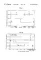
- FIG. 1is a graph showing a difference in Pt contamination level when cleaning solutions of the present invention and cleaning solutions of prior art were used.
- FIG. 2is a graph showing a difference in removability of Pt contaminant when the concentration of hydrochloric acid was changed.
- FIG. 3is a schematic sectional view of an example of the semiconductor device to which the cleaning operation of the present invention is applicable.
- the metal-removing solution used in the present inventionthere can be mentioned a mixture of an inorganic acid (e.g. hydrochloric acid or sulfuric acid) and hydrogen peroxide.
- an inorganic acide.g. hydrochloric acid or sulfuric acid
- hydrogen peroxidee.g. hydrochloric acid or sulfuric acid
- hydrochloric acidis preferred.
- a cleaning solutioncontaining (1) components (e.g. a combination of hydrochloric acid and hydrogen peroxide) capable of forming hypochlorous acid in the cleaning system and (2) a very small amount, preferably 1% by weight or less of hydrofluoric acid.
- An aqueous hypochlorous acid solutionis very unstable and is ordinarily marketed in the form of a hypochlorite such as sodium hypochlorite, potassium hypochlorite or the like; however, the hypochlorite is not usable in the present invention because it contains a cation which adversely affects semiconductor device elements.
- use of unstable hypochlorous acidhas been made possible by using combined components capable of generating hypochlorous acid in the cleaning system.
- Hydrochloric acidreacts with hydrogen peroxide to generate hypochlorous acid.
- This hypochlorous acidacts on a platinum group metal (e.g. Pt or Ir) to form, via a chloride (e.g. platinum chloride or iridium chloride) or directly, tetrachloroplatinic acid ion (H[PtCl 4 ] ⁇ ) or tetrachloroiridic acid ion (H[IrCl 4 ] ⁇ ). Since this ion is soluble and does not remain in a suspended form in the cleaning solution, it is thought that the readhesion of such an ion on substrate can be prevented by washing the substrate with water at pulling-up from the cleaning bath.
- a platinum group metale.g. Pt or Ir
- DHF0.1 wt. % aqueous hydrofluoric acid solution
- the above treatmentwas conducted at a solution temperature of 65° C. when a hydrochloric acid-based cleaning solution was used, and at a temperature of 130° C. when a sulfuric acid-based cleaning solution was used.
- the measurement of Pt contamination levelwas made by wafer surface treatment using hot aqua regia recovery solution and ICP-MS
- FIG. 2is a graph showing the effect of removal of Pt contaminant when hydrochloric acid concentration was changed.
- the Pt removal effectwas high in a hydrochloric acid concentration range of 10 to 25% by weight.
- the hydrochloric acid concentrationis low (the concentration of hydrogen peroxide is relatively high)
- the once formed hypochlorous acidreacts with hydrogen peroxide and returns to hydrochloric acid and, as a result, the amount of hypochlorous acid formed becomes insufficient.
- the amount of hydrogen peroxide usedis preferably about 2 to 5% by weight.
- the amount of hydrofluoric acid usedcan be selected at an optimum level in view of the desired etching rate of silicon oxide film, but is preferably about 1% by weight or less. An amount larger than that is possible when there is used a silicon-based insulating film other than silicon oxide film, such as silicon nitride film, silicon oxide nitride film or the like.
- the amount of hydrofluoric acid usedis preferably determined so that the etching rate of silicon oxide film becomes 1 to 5 nm/min.
- the cleaning solution of the present inventionhas no sufficiently long life; therefore, it is desired in the present invention to mix hydrogen peroxide right before the cleaning operation.
- the cleaning solutionis used at a temperature of room temperature (25° C.) to lower than the boiling point of the cleaning solution, preferably about 50 to 70° C.
- the time of cleaningcan be appropriately varied depending upon, for example, the amounts of hydrochloric acid and hydrogen peroxide used and the temperature of cleaning solution used.
- the cleaning timeis ordinarily 1 to 15 minutes, preferably about 5 to 10 minutes.
Landscapes
- Chemical & Material Sciences (AREA)
- Engineering & Computer Science (AREA)
- Organic Chemistry (AREA)
- Chemical Kinetics & Catalysis (AREA)
- Oil, Petroleum & Natural Gas (AREA)
- Mechanical Engineering (AREA)
- Metallurgy (AREA)
- Materials Engineering (AREA)
- Inorganic Chemistry (AREA)
- Life Sciences & Earth Sciences (AREA)
- General Chemical & Material Sciences (AREA)
- Wood Science & Technology (AREA)
- Condensed Matter Physics & Semiconductors (AREA)
- Physics & Mathematics (AREA)
- General Physics & Mathematics (AREA)
- Manufacturing & Machinery (AREA)
- Computer Hardware Design (AREA)
- Microelectronics & Electronic Packaging (AREA)
- Power Engineering (AREA)
- Cleaning Or Drying Semiconductors (AREA)
- Weting (AREA)
Abstract
Description
Claims (11)
Applications Claiming Priority (2)
| Application Number | Priority Date | Filing Date | Title |
|---|---|---|---|
| JP10-263482 | 1998-09-17 | ||
| JP26348298AJP3189892B2 (en) | 1998-09-17 | 1998-09-17 | Semiconductor substrate cleaning method and cleaning liquid |
Publications (1)
| Publication Number | Publication Date |
|---|---|
| US6432836B1true US6432836B1 (en) | 2002-08-13 |
Family
ID=17390131
Family Applications (1)
| Application Number | Title | Priority Date | Filing Date |
|---|---|---|---|
| US09/393,686Expired - LifetimeUS6432836B1 (en) | 1998-09-17 | 1999-09-10 | Cleaning method for semiconductor substrate and cleaning solution |
Country Status (4)
| Country | Link |
|---|---|
| US (1) | US6432836B1 (en) |
| JP (1) | JP3189892B2 (en) |
| KR (1) | KR20000023187A (en) |
| TW (1) | TW424275B (en) |
Cited By (12)
| Publication number | Priority date | Publication date | Assignee | Title |
|---|---|---|---|---|
| US20040005787A1 (en)* | 2002-07-02 | 2004-01-08 | Taiwan Semiconductor Manufacturing Co., Ltd. | Method to reduce residual particulate contamination in CVD and PVD semiconductor wafer manufacturing |
| US20060051961A1 (en)* | 2004-09-07 | 2006-03-09 | International Business Machines Corporation | Method and process for forming a self-aligned silicide contact |
| US20060177988A1 (en)* | 2004-05-06 | 2006-08-10 | Shea Kevin R | Semiconductor fabrication processes |
| US20060266737A1 (en)* | 2005-05-27 | 2006-11-30 | Hanestad Ronald J | Process for removal of metals and alloys from a substrate |
| US20080090369A1 (en)* | 2006-10-11 | 2008-04-17 | Fujitsu Limited | Method of manufacturing semiconductor device |
| US20080163905A1 (en)* | 2007-01-10 | 2008-07-10 | Jianshe Tang | Two step process for post ash cleaning for Cu/low-k dual damascene structure with metal hard mask |
| EP1950326A1 (en)* | 2007-01-29 | 2008-07-30 | Interuniversitair Microelektronica Centrum | Method for removal of bulk metal contamination from III-V semiconductor substrates |
| US20100112728A1 (en)* | 2007-03-31 | 2010-05-06 | Advanced Technology Materials, Inc. | Methods for stripping material for wafer reclamation |
| EP1975987A3 (en)* | 2007-03-31 | 2011-03-09 | Advanced Technology Materials, Inc. | Methods for stripping material for wafer reclamation |
| US20120273010A1 (en)* | 2011-04-27 | 2012-11-01 | Intermolecular, Inc. | Composition and Method to Remove Excess Material During Manufacturing of Semiconductor Devices |
| US8784572B2 (en) | 2011-10-19 | 2014-07-22 | Intermolecular, Inc. | Method for cleaning platinum residues on a semiconductor substrate |
| US9831088B2 (en) | 2010-10-06 | 2017-11-28 | Entegris, Inc. | Composition and process for selectively etching metal nitrides |
Families Citing this family (9)
| Publication number | Priority date | Publication date | Assignee | Title |
|---|---|---|---|---|
| JP3177973B2 (en) | 1999-01-28 | 2001-06-18 | 日本電気株式会社 | Method for manufacturing semiconductor device |
| JP3358604B2 (en)* | 1999-11-11 | 2002-12-24 | 日本電気株式会社 | Platinum group impurity recovery liquid and its recovery method |
| KR100466310B1 (en)* | 2002-11-13 | 2005-01-14 | 삼성전자주식회사 | Method for manufacturing Metal-Insulator-Metal capacitor |
| KR100639710B1 (en) | 2005-03-17 | 2006-10-30 | 세메스 주식회사 | Chemical mixture supply method |
| JP5464239B2 (en)* | 2006-10-11 | 2014-04-09 | 富士通セミコンダクター株式会社 | Manufacturing method of semiconductor device |
| TWI517235B (en) | 2013-03-01 | 2016-01-11 | 栗田工業股份有限公司 | Semiconductor substrate cleaning system and cleaning method of semiconductor substrate |
| KR102572755B1 (en) | 2018-09-13 | 2023-08-30 | 동우 화인켐 주식회사 | Photoresist cleaning composition |
| KR102572758B1 (en) | 2018-09-17 | 2023-08-30 | 동우 화인켐 주식회사 | Photoresist cleaning composition |
| CN114456884A (en)* | 2021-12-30 | 2022-05-10 | 安莱博医药(苏州)有限公司 | ICP component cleaning agent |
Citations (11)
| Publication number | Priority date | Publication date | Assignee | Title |
|---|---|---|---|---|
| US4398344A (en)* | 1982-03-08 | 1983-08-16 | International Rectifier Corporation | Method of manufacture of a schottky using platinum encapsulated between layers of palladium sintered into silicon surface |
| US4804438A (en)* | 1988-02-08 | 1989-02-14 | Eastman Kodak Company | Method of providing a pattern of conductive platinum silicide |
| JPH03228327A (en)* | 1990-02-02 | 1991-10-09 | Nec Corp | Cleaning method of semiconductor wafer |
| JPH056884A (en)* | 1991-06-27 | 1993-01-14 | Kawasaki Steel Corp | Silicon wafer cleaning method |
| US5258093A (en)* | 1992-12-21 | 1993-11-02 | Motorola, Inc. | Procss for fabricating a ferroelectric capacitor in a semiconductor device |
| JPH06333898A (en)* | 1993-03-23 | 1994-12-02 | Matsushita Electric Ind Co Ltd | Semiconductor device cleaning method and device |
| JPH0745580A (en)* | 1993-08-02 | 1995-02-14 | Toshiba Corp | Semiconductor wafer processing method |
| JPH07130702A (en)* | 1993-11-08 | 1995-05-19 | Fujitsu Ltd | Method for patterning metal film made of platinum or palladium |
| JPH07193035A (en)* | 1993-12-27 | 1995-07-28 | Sumitomo Chem Co Ltd | Method for recovering impurity elements on the surface of a silicon wafer |
| JPH0831781A (en)* | 1994-07-13 | 1996-02-02 | Sony Corp | Washing chemicals |
| JP3228327B2 (en) | 1997-12-22 | 2001-11-12 | 日本電気株式会社 | Semiconductor device |
- 1998
- 1998-09-17JPJP26348298Apatent/JP3189892B2/ennot_activeExpired - Lifetime
- 1999
- 1999-09-10USUS09/393,686patent/US6432836B1/ennot_activeExpired - Lifetime
- 1999-09-15KRKR1019990039632Apatent/KR20000023187A/ennot_activeCeased
- 1999-09-16TWTW088116010Apatent/TW424275B/ennot_activeIP Right Cessation
Patent Citations (11)
| Publication number | Priority date | Publication date | Assignee | Title |
|---|---|---|---|---|
| US4398344A (en)* | 1982-03-08 | 1983-08-16 | International Rectifier Corporation | Method of manufacture of a schottky using platinum encapsulated between layers of palladium sintered into silicon surface |
| US4804438A (en)* | 1988-02-08 | 1989-02-14 | Eastman Kodak Company | Method of providing a pattern of conductive platinum silicide |
| JPH03228327A (en)* | 1990-02-02 | 1991-10-09 | Nec Corp | Cleaning method of semiconductor wafer |
| JPH056884A (en)* | 1991-06-27 | 1993-01-14 | Kawasaki Steel Corp | Silicon wafer cleaning method |
| US5258093A (en)* | 1992-12-21 | 1993-11-02 | Motorola, Inc. | Procss for fabricating a ferroelectric capacitor in a semiconductor device |
| JPH06333898A (en)* | 1993-03-23 | 1994-12-02 | Matsushita Electric Ind Co Ltd | Semiconductor device cleaning method and device |
| JPH0745580A (en)* | 1993-08-02 | 1995-02-14 | Toshiba Corp | Semiconductor wafer processing method |
| JPH07130702A (en)* | 1993-11-08 | 1995-05-19 | Fujitsu Ltd | Method for patterning metal film made of platinum or palladium |
| JPH07193035A (en)* | 1993-12-27 | 1995-07-28 | Sumitomo Chem Co Ltd | Method for recovering impurity elements on the surface of a silicon wafer |
| JPH0831781A (en)* | 1994-07-13 | 1996-02-02 | Sony Corp | Washing chemicals |
| JP3228327B2 (en) | 1997-12-22 | 2001-11-12 | 日本電気株式会社 | Semiconductor device |
Cited By (29)
| Publication number | Priority date | Publication date | Assignee | Title |
|---|---|---|---|---|
| US20040005787A1 (en)* | 2002-07-02 | 2004-01-08 | Taiwan Semiconductor Manufacturing Co., Ltd. | Method to reduce residual particulate contamination in CVD and PVD semiconductor wafer manufacturing |
| US6812156B2 (en)* | 2002-07-02 | 2004-11-02 | Taiwan Semiconductor Manufacturing Co., Ltd | Method to reduce residual particulate contamination in CVD and PVD semiconductor wafer manufacturing |
| US20060258167A1 (en)* | 2004-05-06 | 2006-11-16 | Shea Kevin R | Methods of removing metal-containing materials |
| US20060177988A1 (en)* | 2004-05-06 | 2006-08-10 | Shea Kevin R | Semiconductor fabrication processes |
| US20060258168A1 (en)* | 2004-05-06 | 2006-11-16 | Shea Kevin R | Methods of removing metal-containing materials |
| US20060258166A1 (en)* | 2004-05-06 | 2006-11-16 | Shea Kevin R | Methods of removing metal-containing materials |
| US7683021B2 (en) | 2004-05-06 | 2010-03-23 | Micron Technology, Inc. | Methods of removing metal-containing materials |
| US7683020B2 (en)* | 2004-05-06 | 2010-03-23 | Micron Technology, Inc. | Methods of removing metal-containing materials |
| US7683022B2 (en) | 2004-05-06 | 2010-03-23 | Micron Technology, Inc. | Methods of removing metal-containing materials |
| US7642196B2 (en) | 2004-05-06 | 2010-01-05 | Micron Technology, Inc. | Semiconductor fabrication processes |
| US20080274611A1 (en)* | 2004-09-07 | 2008-11-06 | International Business Machines Corporation | Method and process for forming a self-aligned silicide contact |
| US20060051961A1 (en)* | 2004-09-07 | 2006-03-09 | International Business Machines Corporation | Method and process for forming a self-aligned silicide contact |
| US8101518B2 (en) | 2004-09-07 | 2012-01-24 | International Business Machines Corporation | Method and process for forming a self-aligned silicide contact |
| US7544610B2 (en)* | 2004-09-07 | 2009-06-09 | International Business Machines Corporation | Method and process for forming a self-aligned silicide contact |
| US20060266737A1 (en)* | 2005-05-27 | 2006-11-30 | Hanestad Ronald J | Process for removal of metals and alloys from a substrate |
| WO2006130439A1 (en)* | 2005-05-27 | 2006-12-07 | Fsi International, Inc. | Process for removal of metals and alloys from a substrate |
| US20080090369A1 (en)* | 2006-10-11 | 2008-04-17 | Fujitsu Limited | Method of manufacturing semiconductor device |
| US8679973B2 (en) | 2006-10-11 | 2014-03-25 | Fujitsu Semiconductor Limited | Method of manufacturing semiconductor device |
| US20080163897A1 (en)* | 2007-01-10 | 2008-07-10 | Applied Materials, Inc. | Two step process for post ash cleaning for cu/low-k dual damascene structure with metal hard mask |
| US20080163905A1 (en)* | 2007-01-10 | 2008-07-10 | Jianshe Tang | Two step process for post ash cleaning for Cu/low-k dual damascene structure with metal hard mask |
| US8288291B2 (en) | 2007-01-29 | 2012-10-16 | Imec | Method for removal of bulk metal contamination from III-V semiconductor substrates |
| EP1950326A1 (en)* | 2007-01-29 | 2008-07-30 | Interuniversitair Microelektronica Centrum | Method for removal of bulk metal contamination from III-V semiconductor substrates |
| US20080214013A1 (en)* | 2007-01-29 | 2008-09-04 | Interuniversitair Microelektronica Centrum Vzw (Imec) | Method for Removal of Bulk Metal Contamination from III-V Semiconductor Substrates |
| EP1975987A3 (en)* | 2007-03-31 | 2011-03-09 | Advanced Technology Materials, Inc. | Methods for stripping material for wafer reclamation |
| US20100112728A1 (en)* | 2007-03-31 | 2010-05-06 | Advanced Technology Materials, Inc. | Methods for stripping material for wafer reclamation |
| US9831088B2 (en) | 2010-10-06 | 2017-11-28 | Entegris, Inc. | Composition and process for selectively etching metal nitrides |
| US20120273010A1 (en)* | 2011-04-27 | 2012-11-01 | Intermolecular, Inc. | Composition and Method to Remove Excess Material During Manufacturing of Semiconductor Devices |
| US8894774B2 (en)* | 2011-04-27 | 2014-11-25 | Intermolecular, Inc. | Composition and method to remove excess material during manufacturing of semiconductor devices |
| US8784572B2 (en) | 2011-10-19 | 2014-07-22 | Intermolecular, Inc. | Method for cleaning platinum residues on a semiconductor substrate |
Also Published As
| Publication number | Publication date |
|---|---|
| KR20000023187A (en) | 2000-04-25 |
| JP3189892B2 (en) | 2001-07-16 |
| JP2000100765A (en) | 2000-04-07 |
| TW424275B (en) | 2001-03-01 |
Similar Documents
| Publication | Publication Date | Title |
|---|---|---|
| US6432836B1 (en) | Cleaning method for semiconductor substrate and cleaning solution | |
| US6245650B1 (en) | Process for production of semiconductor device | |
| US7368416B2 (en) | Methods of removing metal-containing materials | |
| US6391793B2 (en) | Compositions for etching silicon with high selectivity to oxides and methods of using same | |
| US6100203A (en) | Methods of employing aqueous cleaning compositions in manufacturing microelectronic devices | |
| JP2005236280A (en) | Semiconductor substrate cleaning liquid composition, semiconductor substrate cleaning method, and conductive structure manufacturing method | |
| JP3645144B2 (en) | Manufacturing method of semiconductor device | |
| US20010039116A1 (en) | Fabrication method for semiconductor device | |
| JP4054887B2 (en) | Ruthenium silicide wet etching method and etchant | |
| JP2001144064A (en) | Cleaning liquid for semiconductor substrate and cleaning method | |
| KR100505175B1 (en) | Ruthenium silicide processing methods | |
| JP2002016053A (en) | Method for manufacturing semiconductor device | |
| US7267127B2 (en) | Method for manufacturing electronic device | |
| JP2005210075A (en) | Semiconductor wafer cleaning method | |
| Kim et al. | The mechanism of poly-Si etching during poly/W gate cleaning by fluorine based cleaning solution | |
| Park et al. | A New Post-Treatment for Chemical-Mechanical Polishing Process of Very Large-Scale Integrated Circuit Tungsten Vias | |
| JP2003045894A (en) | Method for manufacturing semiconductor device | |
| KR970000699B1 (en) | Impurity Wet Cleaning Method on Silicon Substrate Surface Using Reaction Rate Limit | |
| JP2001007072A (en) | Cleaning solution | |
| KR20020046809A (en) | Method For Cleaning The Semiconductor Device | |
| JP2005012113A (en) | Manufacturing method of semiconductor device |
Legal Events
| Date | Code | Title | Description |
|---|---|---|---|
| AS | Assignment | Owner name:NEC CORPORATION, JAPAN Free format text:ASSIGNMENT OF ASSIGNORS INTEREST;ASSIGNOR:WATANABE, KAORI;REEL/FRAME:010252/0095 Effective date:19990907 | |
| STCF | Information on status: patent grant | Free format text:PATENTED CASE | |
| FEPP | Fee payment procedure | Free format text:PAYOR NUMBER ASSIGNED (ORIGINAL EVENT CODE: ASPN); ENTITY STATUS OF PATENT OWNER: LARGE ENTITY | |
| AS | Assignment | Owner name:NEC ELECTRONICS CORPORATION, JAPAN Free format text:ASSIGNMENT OF ASSIGNORS INTEREST;ASSIGNOR:NEC CORPORATION;REEL/FRAME:013774/0295 Effective date:20021101 | |
| FPAY | Fee payment | Year of fee payment:4 | |
| FPAY | Fee payment | Year of fee payment:8 | |
| AS | Assignment | Owner name:RENESAS ELECTRONICS CORPORATION, JAPAN Free format text:CHANGE OF NAME;ASSIGNOR:NEC ELECTRONICS CORPORATION;REEL/FRAME:025375/0948 Effective date:20100401 | |
| REMI | Maintenance fee reminder mailed | ||
| FPAY | Fee payment | Year of fee payment:12 | |
| SULP | Surcharge for late payment | Year of fee payment:11 | |
| AS | Assignment | Owner name:TESSERA ADVANCED TECHNOLOGIES, INC., CALIFORNIA Free format text:ASSIGNMENT OF ASSIGNORS INTEREST;ASSIGNOR:RENESAS ELECTRONICS CORPORATION;REEL/FRAME:032892/0212 Effective date:20140318 | |
| AS | Assignment | Owner name:ROYAL BANK OF CANADA, AS COLLATERAL AGENT, CANADA Free format text:SECURITY INTEREST;ASSIGNORS:INVENSAS CORPORATION;TESSERA, INC.;TESSERA ADVANCED TECHNOLOGIES, INC.;AND OTHERS;REEL/FRAME:040797/0001 Effective date:20161201 | |
| AS | Assignment | Owner name:TESSERA, INC., CALIFORNIA Free format text:RELEASE BY SECURED PARTY;ASSIGNOR:ROYAL BANK OF CANADA;REEL/FRAME:052920/0001 Effective date:20200601 Owner name:PHORUS, INC., CALIFORNIA Free format text:RELEASE BY SECURED PARTY;ASSIGNOR:ROYAL BANK OF CANADA;REEL/FRAME:052920/0001 Effective date:20200601 Owner name:DTS, INC., CALIFORNIA Free format text:RELEASE BY SECURED PARTY;ASSIGNOR:ROYAL BANK OF CANADA;REEL/FRAME:052920/0001 Effective date:20200601 Owner name:FOTONATION CORPORATION (F/K/A DIGITALOPTICS CORPORATION AND F/K/A DIGITALOPTICS CORPORATION MEMS), CALIFORNIA Free format text:RELEASE BY SECURED PARTY;ASSIGNOR:ROYAL BANK OF CANADA;REEL/FRAME:052920/0001 Effective date:20200601 Owner name:DTS LLC, CALIFORNIA Free format text:RELEASE BY SECURED PARTY;ASSIGNOR:ROYAL BANK OF CANADA;REEL/FRAME:052920/0001 Effective date:20200601 Owner name:TESSERA ADVANCED TECHNOLOGIES, INC, CALIFORNIA Free format text:RELEASE BY SECURED PARTY;ASSIGNOR:ROYAL BANK OF CANADA;REEL/FRAME:052920/0001 Effective date:20200601 Owner name:IBIQUITY DIGITAL CORPORATION, MARYLAND Free format text:RELEASE BY SECURED PARTY;ASSIGNOR:ROYAL BANK OF CANADA;REEL/FRAME:052920/0001 Effective date:20200601 Owner name:INVENSAS BONDING TECHNOLOGIES, INC. (F/K/A ZIPTRONIX, INC.), CALIFORNIA Free format text:RELEASE BY SECURED PARTY;ASSIGNOR:ROYAL BANK OF CANADA;REEL/FRAME:052920/0001 Effective date:20200601 Owner name:INVENSAS CORPORATION, CALIFORNIA Free format text:RELEASE BY SECURED PARTY;ASSIGNOR:ROYAL BANK OF CANADA;REEL/FRAME:052920/0001 Effective date:20200601 |