US6432814B1 - Method of manufacturing an interconnect structure having a passivation layer for preventing subsequent processing reactions - Google Patents
Method of manufacturing an interconnect structure having a passivation layer for preventing subsequent processing reactionsDownload PDFInfo
- Publication number
- US6432814B1 US6432814B1US09/727,195US72719500AUS6432814B1US 6432814 B1US6432814 B1US 6432814B1US 72719500 AUS72719500 AUS 72719500AUS 6432814 B1US6432814 B1US 6432814B1
- Authority
- US
- United States
- Prior art keywords
- forming
- passivation layer
- opening
- substrate
- recited
- Prior art date
- Legal status (The legal status is an assumption and is not a legal conclusion. Google has not performed a legal analysis and makes no representation as to the accuracy of the status listed.)
- Expired - Lifetime
Links
Images


Classifications
- H—ELECTRICITY
- H01—ELECTRIC ELEMENTS
- H01L—SEMICONDUCTOR DEVICES NOT COVERED BY CLASS H10
- H01L21/00—Processes or apparatus adapted for the manufacture or treatment of semiconductor or solid state devices or of parts thereof
- H01L21/70—Manufacture or treatment of devices consisting of a plurality of solid state components formed in or on a common substrate or of parts thereof; Manufacture of integrated circuit devices or of parts thereof
- H01L21/71—Manufacture of specific parts of devices defined in group H01L21/70
- H01L21/768—Applying interconnections to be used for carrying current between separate components within a device comprising conductors and dielectrics
- H01L21/76801—Applying interconnections to be used for carrying current between separate components within a device comprising conductors and dielectrics characterised by the formation and the after-treatment of the dielectrics, e.g. smoothing
- H01L21/76802—Applying interconnections to be used for carrying current between separate components within a device comprising conductors and dielectrics characterised by the formation and the after-treatment of the dielectrics, e.g. smoothing by forming openings in dielectrics
- H01L21/76807—Applying interconnections to be used for carrying current between separate components within a device comprising conductors and dielectrics characterised by the formation and the after-treatment of the dielectrics, e.g. smoothing by forming openings in dielectrics for dual damascene structures
- H01L21/76808—Applying interconnections to be used for carrying current between separate components within a device comprising conductors and dielectrics characterised by the formation and the after-treatment of the dielectrics, e.g. smoothing by forming openings in dielectrics for dual damascene structures involving intermediate temporary filling with material
- H—ELECTRICITY
- H01—ELECTRIC ELEMENTS
- H01L—SEMICONDUCTOR DEVICES NOT COVERED BY CLASS H10
- H01L2221/00—Processes or apparatus adapted for the manufacture or treatment of semiconductor or solid state devices or of parts thereof covered by H01L21/00
- H01L2221/10—Applying interconnections to be used for carrying current between separate components within a device
- H01L2221/1005—Formation and after-treatment of dielectrics
- H01L2221/1052—Formation of thin functional dielectric layers
- H01L2221/1057—Formation of thin functional dielectric layers in via holes or trenches
- H01L2221/1063—Sacrificial or temporary thin dielectric films in openings in a dielectric
- Y—GENERAL TAGGING OF NEW TECHNOLOGICAL DEVELOPMENTS; GENERAL TAGGING OF CROSS-SECTIONAL TECHNOLOGIES SPANNING OVER SEVERAL SECTIONS OF THE IPC; TECHNICAL SUBJECTS COVERED BY FORMER USPC CROSS-REFERENCE ART COLLECTIONS [XRACs] AND DIGESTS
- Y10—TECHNICAL SUBJECTS COVERED BY FORMER USPC
- Y10S—TECHNICAL SUBJECTS COVERED BY FORMER USPC CROSS-REFERENCE ART COLLECTIONS [XRACs] AND DIGESTS
- Y10S438/00—Semiconductor device manufacturing: process
- Y10S438/958—Passivation layer
Definitions
- the present inventionis directed, in general, to a method of semiconductor fabrication and, more specifically, to a method of manufacturing an interconnect structure within a substrate employing a passivation layer to inhibit the diffusion of elements from the substrate.
- VLSIDeep ultra-violet
- DUVDeep ultra-violet
- Low dielectric constant (low k) inter-metal dielectricsare used in order to improve performance by reducing parasitic capacitance.
- Copper interconnects, which improve performance due to copper's low resistance,have also recently gained wide acceptance. These copper interconnects are typically formed using damascene or dual damascene processes to define the interconnect paths, and are typically used in conjunction with porous dielectric materials that have low dielectric constants (low k).
- One approach of the damascene processis a full via first approach, which provides lower cost processing, improved level-level alignment tolerance and thus tighter design rules and improved performance.
- the full via first approachvia holes are etched first, and then the trench is etched. The full via first is etched down to the copper or previous a layer of dielectric using the dual damascene process.
- One problem associated with the full via first dual damascene approachis its integration with chemically amplified DUV photo resist (PR) systems. Because etch selectivity is needed when etching the via, nitrogen is added to the chemistry. However, the added nitrogen, in its radical form, diffuses into the porous, low k material. When trench lithography is performed, a DUV photoresist is put down into the via. The photoresist contains photo acid generators that are activated by DUV, thus forming photo acid catalysts.
- PRchemically amplified DUV photo resist
- the photo acid catalystswork to break the bonds of the photoresist, the photoresist then becomes soluble amino groups (weak base) that were previously lodged in the porous low k material freely leach out into the photoresist and interact with the photo acid catalyst (weak acid) and renders the photo acid catalyst inactive. This, in turn, prevents the photoresist from developing properly, which results in unwanted dome-like features, which cannot easily be removed.
- the present inventionprovides a method of manufacturing an interconnect structure within a substrate.
- the methodincludes forming an opening in a substrate.
- the substratemay be a dielectric layer having a low dielectric constant; for example, one where the dielectric constant ranges from about 3.9 to about 1.9.
- This particular embodimentfurther includes forming a passivation layer within the opening and a photoresist within the opening and over the passivation layer.
- the passivation layerinhibits the diffusion of elements from the substrate that can deactivate a photo acid generator (PAG) within the photoresist, which inhibits the photoresist from developing properly.
- PAGphoto acid generator
- the photoresistDue to the presence of the passivation layer, the photoresist is able to develop properly, which prevents the formation of photoresist anomalies, as found in prior art process. Thus, the presence of the passivation layer addresses the problems associated with the above-discussed prior art processes.
- FIG. 1illustrates a partial sectional view of an exemplary embodiment of an interconnect structure 100 ;
- FIG. 2illustrates a partial sectional view of an interconnect structure where the photoresist (PR) is deposited
- FIG. 3illustrates a partial sectional view of an interconnect structure showing formation of via openings in the interconnect structure of FIG. 2;
- FIG. 4illustrates a partial sectional view of an interconnect structure showing deposition of a passivation layer of the present invention, within the via opening and over the second substrate layer of FIG. 3;
- FIG. 5illustrates a partial sectional view of an interconnect structure showing deposition and patterning of another photoresist layer to the interconnect structure of FIG. 4;
- FIG. 6illustrates a partial sectional view of an interconnect structure after the photoresist layer is patterned to embody the shape of a trench opening
- FIG. 7illustrates a partial sectional view of an interconnect structure showing a dielectric etch that forms trench opening to interconnect structure of FIG. 6;
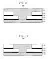
- FIG. 8illustrates a partial sectional view of an interconnect structure showing an etch of the first etch stop layer of the interconnect structure of FIG. 7;
- FIG. 9illustrate a partial sectional view of an interconnect structure showing a conductive material deposited within the openings
- FIG. 10illustrate a partial sectional view of an interconnect structure showing the conductive material planarized back to the second substrate layer
- FIG. 11illustrates a partial sectional view of a combined 20 interconnect structure incorporating an embodiment of the interconnect structure as fabricated in FIGS. 1-10, and a conventionally formed integrated circuit (IC) that may be used in conjunction with the present invention.
- ICintegrated circuit
- the intermediate structure 100includes a metal layer 110 located on a surface of a semiconductor wafer substrate, an optional first etch stop layer 115 , a first dielectric layer 120 , a second etch stop layer 125 , and second dielectric layer 130 , all of which can be deposited with conventional deposition processes and materials.
- the metal layer 110is first formed by conventionally depositing a conductive layer of metal, such as copper. While the first metal layer 110 is shown as a continuous layer, it should be understood that this is for illustrative purposes only and that the metal layer 110 will typically be patterned into multiple separate features.
- the first dielectric layer 120is conventionally formed over the first etch stop layer 115 , if present, and the second etch stop layer 125 is conventionally formed over the first substrate layer 120 . Silicon nitride or other similar etch stop materials may be used to form the first and second etch stop layers 115 , 125 .
- the second dielectric layer 130is formed over the etch stop layer 125 .
- the first and second dielectric layers 120 and 130may be low k material.
- the dielectric layers 120 , 130may have dielectric constants that range from about 3.8 to about 1.9.
- low k materialsinclude CVD formation of fluorinated oxide (FSG) having a dielectric constant of about 3.6, and spin on formation of hydrogen silsesquioxane (HSQ) having a dielectric constant of about 2.9.
- FSGfluorinated oxide
- HSQhydrogen silsesquioxane
- Further examples of low k materialsinclude organic polymers like polyarylenes and polyarylene-ethers, which include SiLKTM (Dow Chemical-Midland, Mich.) and FLARETM (AlliedSignal-Morristown, N.J.).
- first and second dielectric substrate layers 120 , 130may also be formed from other appropriate dielectric materials having the appropriate low-k.
- the second etch stop layer 125located over the first substrate layer 120 , may be formed from other available or future developed dielectric materials.
- the metal layer 110 and the first and second etch stop layers 115 , 125are not limited to the materials disclosed above.
- the metal layer 110may include other appropriate conductor metals used in integrated circuit design as other applications or embodiments may require.
- the first and second substrate layers 120 , 130may typically be formed by methods that include but are not limited to chemical vapor deposition, physical vapor deposition, such as high density plasma deposition processes, or a conventional spin on technique, to a thickness ranging from about 300 nm to about 1000 nm.
- the etch stop layer 125may typically have a thickness ranging from about 15 nm to about 100 nm, and it may be deposited by conventional plasma enhanced chemical vapor deposition or other similar process.
- One skilled in the artunderstands that the present invention may use varying thicknesses of the various layers depending on the design of the device.
- the photoresist 210is deposited over the second substrate layer 130 with conventional deposition processes and materials.
- Typical photoresist used for trench lithographyare aromatic substituted photoresist. Examples of such photoresists include hybrid-type photoresist, acetal, and S-CAP. Other photoresists include trade names such as Shipley UVG, Sumittomo 318, TOK 308 or PO. 65.
- the photoresist layer 210is then conventionally patterned for via opening 220 as illustrated in FIG. 2 .
- FIG. 3illustrated is a partial sectional view of an interconnect structure 300 showing formation of a first full via opening 310 that extends to the metal layer 110 in the interconnect structure 200 of FIG. 2 .
- the via opening 310is formed as patterned by the photoresist 210 of FIG. 2, through the second substrate layer 130 , the second etch stop layer 125 and the first substrate level 120 .
- the first and second substrate layers 120 , 130are etched using conventional dielectric etching processes and the second etch stop layer 125 is also etched using conventional processes, such as by using a hesafluoride (SF6) etch.
- SF6hesafluoride
- FIG. 4illustrated is a partial sectional view of an interconnect structure 400 showing deposition of a passivation layer 410 within the first full via opening 310 of FIG. 3 and over the second substrate layer 130 .
- the application of the passivation layer 410may use a conventional spin on technique. While a conventional spin on technique may be used to deposit the passivation layer 410 , other methods, such as chemical vapor deposition or physical vapor deposition, may be used.
- the thickness of the passivation layer 410may range from about 5 nm to about 100 nm; however, the thickness of the passivation layer 410 may depend on the size of the first full via opening 310 and is, thus, not necessarily limited to this range.
- the passivation layer 410substantially inhibits the diffusion of elements, such as nitrogen, from the first and second substrate layers 120 , 130 that may leach into the photoresist 510 and deactivate the photoresist's photo acid catalyst.
- the presence of the passivation layer 410substantially inhibits or prevents the formation of the photoresist anomalies associated with the above-discussed prior art processes.
- the passivation layer 410includes an organic polymer.
- this organic polymerincludes a hydrophobic acrylate.
- this hydrophobic acrylateis a methyl methacrylate or a flouro-methacrylate.
- FIG. 5illustrated is a partial sectional view of an intermediate interconnect structure 500 showing deposition of photoresist layer 510 to the interconnect structure 400 of FIG. 4 .
- the photoresist layer 510is conventionally deposited within the via opening 420 of FIG. 4 and over the passivation layer 410 .
- the low-k dielectric layers 120 , 130typically have nitrogen incorporated therein, which tends to diffuse into the photoresist 510 in the absence of the passivation layer 410 .
- the nitrogenis substantially prevented from diffusing into the photoresist 510 due to the presence of the passivation layer 410 .
- the nitrogendoes not interfere with the proper development of the photoresist 510 , which substantially or completely eliminates the photoresist anomalies often associated with prior art process that are discussed above.
- the photoresist layer 510is deposited it is patterned to embody the shape illustrated in FIG. 6 for a trench opening.
- the via opening 620in advantageous embodiments, may ultimately become an interconnect structure formed by a dual damascene process.
- the present inventionis, therefore, particularly advantageous when conducted with damascene processes, however, it is not limited to such applications.
- an etchis conducted that forms trench opening 720 over the via opening 710 that connects with conductive layer 110 .
- the passivation layer 410 and the second substrate layer 130are etched using any conventional dielectric etching processes, such as by using a hesafluoride (SF 6 ) etch.
- the passivation layer 410will etch in chemistry similar to that used to etch the dielectric layers 120 , 130 .
- etch chemistrysuch as C 4 F 8 or CF 4 with O 2 or CO 2 and N 2 is used.
- FIG. 8illustrated is a partial sectional view of an interconnect structure 800 showing a conventional etch of the first etch stop layer 115 and second etch stop layer 125 of the interconnect structure 700 of FIG. 7 .
- the trench openingmay be etched through the second etch stop layer 125 to the first dielectric layer 120 .
- the photoresist 730 of FIG. 7 and the remaining passivation layer 410are conventionally removed, resulting in the interconnect structure 800 of FIG. 8 .
- the trench opening 820 and the via opening 810are cleaned, which results in interconnect structure 800 .
- a conductive material 910such as copper, may be deposited within the openings to form interconnect structure 900 of FIG. 9 .
- the conductive materialis planarized back to the second substrate layer 130 to form the interconnect structure 1000 of FIG. 10 .
- the planarizationis achieved either by etch back or chemical mechanical polishing.
- FIG. 11illustrates a partial sectional view of a combined interconnect structure 1100 incorporating an embodiment of the interconnect structure 1000 as shown in FIG. 10 and discussed above, and a conventionally formed integrated circuit (IC) 1101 that may be used in conjunction with the present invention. While FIG. 11 does not specifically illustrate how the interconnect structure described in FIGS. 1-10 is electrically connected to the IC 1101 , one who is skilled in the art understands how to make such a connection, and integrate the interconnect structure, as provided herein, into the IC 1101 .
- the IC 1101includes conventional transistors 1110 that are connected by a via 1120 , as covered by the present invention or by more conventional interconnects 1125 , such as damascene structures.
- the via 1120shows an illustrative embodiment of the present invention.
- Dielectric layers 1130 , 1132 and 1134isolate the various layers of the IC 1100 .
- the transistors 1110are located on a semiconductor wafer substrate (generally designated 1105 ), and the via 1120 , which is located within the dielectric layers 1130 1132 , connect the transistors 1110 to different layers within the IC circuit 1100 .
- forming the transistors 1110may include forming semiconductor devices, such as a complementary metal oxide semiconductor device, a merged bipolar and complementary metal oxide semiconductor device, or a bipolar semiconductor device.
- the transistors 1110include conventionally formed tubs 1135 , source/drains 1140 , gate oxides 1145 and gates 1150 .
- One who is skilled in the artknows how to fabricate the transistors 1110 interconnects or vias 1125 and dielectric layers 1130 , 1132 and 1134 .
- multiple transistors 1110 , vias 1120 and dielectric layers 1130 , 1132 , and 1134are typically interconnected to form the IC 1101.
Landscapes
- Engineering & Computer Science (AREA)
- Physics & Mathematics (AREA)
- Condensed Matter Physics & Semiconductors (AREA)
- General Physics & Mathematics (AREA)
- Manufacturing & Machinery (AREA)
- Computer Hardware Design (AREA)
- Microelectronics & Electronic Packaging (AREA)
- Power Engineering (AREA)
- Internal Circuitry In Semiconductor Integrated Circuit Devices (AREA)
Abstract
Description
Claims (20)
Priority Applications (1)
| Application Number | Priority Date | Filing Date | Title |
|---|---|---|---|
| US09/727,195US6432814B1 (en) | 2000-11-30 | 2000-11-30 | Method of manufacturing an interconnect structure having a passivation layer for preventing subsequent processing reactions |
Applications Claiming Priority (1)
| Application Number | Priority Date | Filing Date | Title |
|---|---|---|---|
| US09/727,195US6432814B1 (en) | 2000-11-30 | 2000-11-30 | Method of manufacturing an interconnect structure having a passivation layer for preventing subsequent processing reactions |
Publications (2)
| Publication Number | Publication Date |
|---|---|
| US20020064940A1 US20020064940A1 (en) | 2002-05-30 |
| US6432814B1true US6432814B1 (en) | 2002-08-13 |
Family
ID=24921711
Family Applications (1)
| Application Number | Title | Priority Date | Filing Date |
|---|---|---|---|
| US09/727,195Expired - LifetimeUS6432814B1 (en) | 2000-11-30 | 2000-11-30 | Method of manufacturing an interconnect structure having a passivation layer for preventing subsequent processing reactions |
Country Status (1)
| Country | Link |
|---|---|
| US (1) | US6432814B1 (en) |
Cited By (14)
| Publication number | Priority date | Publication date | Assignee | Title |
|---|---|---|---|---|
| US20030017694A1 (en)* | 2001-07-23 | 2003-01-23 | Applied Materials, Inc. | Selective etching of organosilicate films over silicon oxide stop etch layers |
| US6780761B1 (en)* | 2003-08-15 | 2004-08-24 | United Microelectronics Corp. | Via-first dual damascene process |
| US20050062164A1 (en)* | 2003-09-23 | 2005-03-24 | Taiwan Semiconductor Manufacturing Co., Ltd. | Method for improving time dependent dielectric breakdown lifetimes |
| US20050101122A1 (en)* | 2003-11-10 | 2005-05-12 | Sung Bo Hwang | Method for fabricating semiconductor device |
| US20060216929A1 (en)* | 2005-03-28 | 2006-09-28 | Hyun-Mog Park | Etch stopless dual damascene structure and method of fabrication |
| CN1294640C (en)* | 2003-09-03 | 2007-01-10 | 联华电子股份有限公司 | Via-first dual damascene process |
| CN1295776C (en)* | 2003-12-24 | 2007-01-17 | 上海宏力半导体制造有限公司 | Method for separately surface treatment to intermediate window and groove of double inlay |
| US20070082489A1 (en)* | 2005-10-06 | 2007-04-12 | Po-Chao Tsao | Method of fabricating openings and contact holes |
| US20080153295A1 (en)* | 2005-10-06 | 2008-06-26 | Feng-Yi Chang | Method of fabricating openings and contact holes |
| US20080227287A1 (en)* | 2007-03-16 | 2008-09-18 | Taiwan Semiconductor Manufacturing Company, Ltd. | Method For Dual Damascene Process |
| US20100087018A1 (en)* | 2008-10-02 | 2010-04-08 | Xie yong-gang | Method for forming dual damascene structure |
| US20110006437A1 (en)* | 2005-10-06 | 2011-01-13 | Po-Chao Tsao | Opening structure |
| TWI469256B (en)* | 2008-10-02 | 2015-01-11 | United Microelectronics Corp | Method for forming dual damascene structure |
| US9140630B2 (en) | 2005-08-22 | 2015-09-22 | Applied Biosystems, Llc | Device and method for making discrete volumes of a first fluid in contact with a second fluid, which are immiscible with each other |
Families Citing this family (2)
| Publication number | Priority date | Publication date | Assignee | Title |
|---|---|---|---|---|
| TW200428586A (en)* | 2003-04-08 | 2004-12-16 | Matsushita Electric Industrial Co Ltd | Electronic device and the manufacturing method thereof |
| US7504727B2 (en)* | 2004-05-14 | 2009-03-17 | International Business Machines Corporation | Semiconductor interconnect structure utilizing a porous dielectric material as an etch stop layer between adjacent non-porous dielectric materials |
Citations (9)
| Publication number | Priority date | Publication date | Assignee | Title |
|---|---|---|---|---|
| WO1997019462A2 (en)* | 1995-11-22 | 1997-05-29 | Siemens Aktiengesellschaft | Vertically integrated semiconductor component and method of producing the same |
| US5924005A (en)* | 1997-02-18 | 1999-07-13 | Motorola, Inc. | Process for forming a semiconductor device |
| US6054379A (en)* | 1998-02-11 | 2000-04-25 | Applied Materials, Inc. | Method of depositing a low k dielectric with organo silane |
| US6140226A (en)* | 1998-01-16 | 2000-10-31 | International Business Machines Corporation | Dual damascene processing for semiconductor chip interconnects |
| US6200912B1 (en)* | 1995-10-09 | 2001-03-13 | Matsushita Electric Industrial Co., Ltd. | Semiconductor device and method of producing the same |
| US6258732B1 (en)* | 1999-02-04 | 2001-07-10 | International Business Machines Corporation | Method of forming a patterned organic dielectric layer on a substrate |
| US6265303B1 (en)* | 1997-05-28 | 2001-07-24 | Texas Instruments Incorporated | Integrated circuit dielectric and method |
| US6319815B1 (en)* | 1998-10-21 | 2001-11-20 | Tokyo Ohka Kogyo Co., Ltd. | Electric wiring forming method with use of embedding material |
| US6319821B1 (en)* | 2000-04-24 | 2001-11-20 | Taiwan Semiconductor Manufacturing Company | Dual damascene approach for small geometry dimension |
- 2000
- 2000-11-30USUS09/727,195patent/US6432814B1/ennot_activeExpired - Lifetime
Patent Citations (10)
| Publication number | Priority date | Publication date | Assignee | Title |
|---|---|---|---|---|
| US6200912B1 (en)* | 1995-10-09 | 2001-03-13 | Matsushita Electric Industrial Co., Ltd. | Semiconductor device and method of producing the same |
| WO1997019462A2 (en)* | 1995-11-22 | 1997-05-29 | Siemens Aktiengesellschaft | Vertically integrated semiconductor component and method of producing the same |
| US6146992A (en)* | 1995-11-22 | 2000-11-14 | Siemens Aktiengesellschaft | Vertically integrated semiconductor component and method of producing the same |
| US5924005A (en)* | 1997-02-18 | 1999-07-13 | Motorola, Inc. | Process for forming a semiconductor device |
| US6265303B1 (en)* | 1997-05-28 | 2001-07-24 | Texas Instruments Incorporated | Integrated circuit dielectric and method |
| US6140226A (en)* | 1998-01-16 | 2000-10-31 | International Business Machines Corporation | Dual damascene processing for semiconductor chip interconnects |
| US6054379A (en)* | 1998-02-11 | 2000-04-25 | Applied Materials, Inc. | Method of depositing a low k dielectric with organo silane |
| US6319815B1 (en)* | 1998-10-21 | 2001-11-20 | Tokyo Ohka Kogyo Co., Ltd. | Electric wiring forming method with use of embedding material |
| US6258732B1 (en)* | 1999-02-04 | 2001-07-10 | International Business Machines Corporation | Method of forming a patterned organic dielectric layer on a substrate |
| US6319821B1 (en)* | 2000-04-24 | 2001-11-20 | Taiwan Semiconductor Manufacturing Company | Dual damascene approach for small geometry dimension |
Non-Patent Citations (1)
| Title |
|---|
| "Lithographic Patterns with a Barrier Liner," IBM Technical Disclosure Bulletin, vol. 32, No. 10B, pp. 114-115, Mar. 1990.* |
Cited By (31)
| Publication number | Priority date | Publication date | Assignee | Title |
|---|---|---|---|---|
| US7244672B2 (en) | 2001-07-23 | 2007-07-17 | Applied Materials, Inc. | Selective etching of organosilicate films over silicon oxide stop etch layers |
| US20030017694A1 (en)* | 2001-07-23 | 2003-01-23 | Applied Materials, Inc. | Selective etching of organosilicate films over silicon oxide stop etch layers |
| US20050255697A1 (en)* | 2001-07-23 | 2005-11-17 | Applied Materials, Inc. | Selective etching of organosilicate films over silicon oxide stop etch layers |
| US7183201B2 (en)* | 2001-07-23 | 2007-02-27 | Applied Materials, Inc. | Selective etching of organosilicate films over silicon oxide stop etch layers |
| US6780761B1 (en)* | 2003-08-15 | 2004-08-24 | United Microelectronics Corp. | Via-first dual damascene process |
| CN1294640C (en)* | 2003-09-03 | 2007-01-10 | 联华电子股份有限公司 | Via-first dual damascene process |
| US20050062164A1 (en)* | 2003-09-23 | 2005-03-24 | Taiwan Semiconductor Manufacturing Co., Ltd. | Method for improving time dependent dielectric breakdown lifetimes |
| US6962874B2 (en)* | 2003-11-10 | 2005-11-08 | Hynix Semiconductor Inc. | Method for fabricating semiconductor device |
| CN1324652C (en)* | 2003-11-10 | 2007-07-04 | 美格纳半导体有限公司 | Method for fabricating semiconductor device |
| US20050101122A1 (en)* | 2003-11-10 | 2005-05-12 | Sung Bo Hwang | Method for fabricating semiconductor device |
| CN1295776C (en)* | 2003-12-24 | 2007-01-17 | 上海宏力半导体制造有限公司 | Method for separately surface treatment to intermediate window and groove of double inlay |
| US20060216929A1 (en)* | 2005-03-28 | 2006-09-28 | Hyun-Mog Park | Etch stopless dual damascene structure and method of fabrication |
| US12435367B2 (en) | 2005-08-22 | 2025-10-07 | Applied Biosystems, Llc | Apparatus, system, and method using immiscible-fluid-discrete-volumes |
| US11319585B2 (en) | 2005-08-22 | 2022-05-03 | Applied Biosystems, Llc | Device and method for making discrete volumes of a first fluid in contact with a second fluid, which are immiscible with each other |
| US11162137B2 (en) | 2005-08-22 | 2021-11-02 | Applied Biosystems Llc | Apparatus, system, and method using immiscible-fluid-discrete-volumes |
| US10450604B2 (en) | 2005-08-22 | 2019-10-22 | Applied Biosystems, Llc | Device and method for making discrete volumes of a first fluid in contact with a second fluid, which are immiscible with each other |
| US10041113B2 (en) | 2005-08-22 | 2018-08-07 | Applied Biosystems, Llc | Apparatus, system, and method using immiscible-fluid-discrete-volumes |
| US9140630B2 (en) | 2005-08-22 | 2015-09-22 | Applied Biosystems, Llc | Device and method for making discrete volumes of a first fluid in contact with a second fluid, which are immiscible with each other |
| US8461649B2 (en) | 2005-10-06 | 2013-06-11 | United Microelectronics Corp. | Opening structure for semiconductor device |
| US8164141B2 (en) | 2005-10-06 | 2012-04-24 | United Microelectronics Corp. | Opening structure with sidewall of an opening covered with a dielectric thin film |
| US8236702B2 (en) | 2005-10-06 | 2012-08-07 | United Microelectronics Corp. | Method of fabricating openings and contact holes |
| US20110006437A1 (en)* | 2005-10-06 | 2011-01-13 | Po-Chao Tsao | Opening structure |
| US8592322B2 (en) | 2005-10-06 | 2013-11-26 | United Microelectronics Corp. | Method of fabricating openings |
| US7825034B2 (en)* | 2005-10-06 | 2010-11-02 | United Microelectronics Corp. | Method of fabricating openings and contact holes |
| US20080153295A1 (en)* | 2005-10-06 | 2008-06-26 | Feng-Yi Chang | Method of fabricating openings and contact holes |
| US20070082489A1 (en)* | 2005-10-06 | 2007-04-12 | Po-Chao Tsao | Method of fabricating openings and contact holes |
| US7642184B2 (en)* | 2007-03-16 | 2010-01-05 | Taiwan Semiconductor Manufacturing Company, Ltd. | Method for dual damascene process |
| US20080227287A1 (en)* | 2007-03-16 | 2008-09-18 | Taiwan Semiconductor Manufacturing Company, Ltd. | Method For Dual Damascene Process |
| US8592229B2 (en)* | 2008-10-02 | 2013-11-26 | United Microelectronics Corp. | Method for forming dual damascene structure |
| TWI469256B (en)* | 2008-10-02 | 2015-01-11 | United Microelectronics Corp | Method for forming dual damascene structure |
| US20100087018A1 (en)* | 2008-10-02 | 2010-04-08 | Xie yong-gang | Method for forming dual damascene structure |
Also Published As
| Publication number | Publication date |
|---|---|
| US20020064940A1 (en) | 2002-05-30 |
Similar Documents
| Publication | Publication Date | Title |
|---|---|---|
| US6184128B1 (en) | Method using a thin resist mask for dual damascene stop layer etch | |
| US6432814B1 (en) | Method of manufacturing an interconnect structure having a passivation layer for preventing subsequent processing reactions | |
| US5886410A (en) | Interconnect structure with hard mask and low dielectric constant materials | |
| US7563719B2 (en) | Dual damascene process | |
| CN100419995C (en) | Dual damascene process | |
| US6951709B2 (en) | Method of fabricating a semiconductor multilevel interconnect structure | |
| US7129162B2 (en) | Dual cap layer in damascene interconnection processes | |
| US8227336B2 (en) | Structure with self aligned resist layer on an interconnect surface and method of making same | |
| US6458705B1 (en) | Method for forming via-first dual damascene interconnect structure | |
| US20020182874A1 (en) | Method for forming hybrid low-k film stack to avoid thermal stress effect | |
| US20070249164A1 (en) | Method of fabricating an interconnect structure | |
| US6624061B2 (en) | Semiconductor device and method of manufacturing the same capable of reducing deterioration of low dielectric constant film | |
| US7285853B2 (en) | Multilayer anti-reflective coating for semiconductor lithography and the method for forming the same | |
| JP2003100724A (en) | Aluminium hard mask for dielectric etching | |
| US6969683B2 (en) | Method of preventing resist poisoning in dual damascene structures | |
| US7323408B2 (en) | Metal barrier cap fabrication by polymer lift-off | |
| US6313025B1 (en) | Process for manufacturing an integrated circuit including a dual-damascene structure and an integrated circuit | |
| US6803314B2 (en) | Double-layered low dielectric constant dielectric dual damascene method | |
| US6365327B1 (en) | Process for manufacturing in integrated circuit including a dual-damascene structure and an integrated circuit | |
| US6780761B1 (en) | Via-first dual damascene process | |
| US20030096496A1 (en) | Method of forming dual damascene structure | |
| US6800548B2 (en) | Method to avoid via poisoning in dual damascene process | |
| US6812142B1 (en) | Method and interlevel dielectric structure for improved metal step coverage | |
| KR20030077455A (en) | Method for manufacturing semiconductor device using dual-damascene techniques | |
| US20020061470A1 (en) | Dual damascene process utilizing a bi-layer imaging layer |
Legal Events
| Date | Code | Title | Description |
|---|---|---|---|
| AS | Assignment | Owner name:LUCENT TECHNOLOGIES, INC., NEW JERSEY Free format text:ASSIGNMENT OF ASSIGNORS INTEREST;ASSIGNORS:STEINER, KURT G.;VITKAVAGE, SUSAN C.;REEL/FRAME:011336/0032 Effective date:20001127 | |
| STCF | Information on status: patent grant | Free format text:PATENTED CASE | |
| FEPP | Fee payment procedure | Free format text:PAYOR NUMBER ASSIGNED (ORIGINAL EVENT CODE: ASPN); ENTITY STATUS OF PATENT OWNER: LARGE ENTITY | |
| FPAY | Fee payment | Year of fee payment:4 | |
| FPAY | Fee payment | Year of fee payment:8 | |
| FPAY | Fee payment | Year of fee payment:12 | |
| AS | Assignment | Owner name:DEUTSCHE BANK AG NEW YORK BRANCH, AS COLLATERAL AG Free format text:PATENT SECURITY AGREEMENT;ASSIGNORS:LSI CORPORATION;AGERE SYSTEMS LLC;REEL/FRAME:032856/0031 Effective date:20140506 | |
| AS | Assignment | Owner name:AVAGO TECHNOLOGIES GENERAL IP (SINGAPORE) PTE. LTD Free format text:ASSIGNMENT OF ASSIGNORS INTEREST;ASSIGNOR:AGERE SYSTEMS LLC;REEL/FRAME:035365/0634 Effective date:20140804 | |
| AS | Assignment | Owner name:LSI CORPORATION, CALIFORNIA Free format text:TERMINATION AND RELEASE OF SECURITY INTEREST IN PATENT RIGHTS (RELEASES RF 032856-0031);ASSIGNOR:DEUTSCHE BANK AG NEW YORK BRANCH, AS COLLATERAL AGENT;REEL/FRAME:037684/0039 Effective date:20160201 Owner name:AGERE SYSTEMS LLC, PENNSYLVANIA Free format text:TERMINATION AND RELEASE OF SECURITY INTEREST IN PATENT RIGHTS (RELEASES RF 032856-0031);ASSIGNOR:DEUTSCHE BANK AG NEW YORK BRANCH, AS COLLATERAL AGENT;REEL/FRAME:037684/0039 Effective date:20160201 | |
| AS | Assignment | Owner name:BANK OF AMERICA, N.A., AS COLLATERAL AGENT, NORTH CAROLINA Free format text:PATENT SECURITY AGREEMENT;ASSIGNOR:AVAGO TECHNOLOGIES GENERAL IP (SINGAPORE) PTE. LTD.;REEL/FRAME:037808/0001 Effective date:20160201 Owner name:BANK OF AMERICA, N.A., AS COLLATERAL AGENT, NORTH Free format text:PATENT SECURITY AGREEMENT;ASSIGNOR:AVAGO TECHNOLOGIES GENERAL IP (SINGAPORE) PTE. LTD.;REEL/FRAME:037808/0001 Effective date:20160201 | |
| AS | Assignment | Owner name:AVAGO TECHNOLOGIES GENERAL IP (SINGAPORE) PTE. LTD., SINGAPORE Free format text:TERMINATION AND RELEASE OF SECURITY INTEREST IN PATENTS;ASSIGNOR:BANK OF AMERICA, N.A., AS COLLATERAL AGENT;REEL/FRAME:041710/0001 Effective date:20170119 Owner name:AVAGO TECHNOLOGIES GENERAL IP (SINGAPORE) PTE. LTD Free format text:TERMINATION AND RELEASE OF SECURITY INTEREST IN PATENTS;ASSIGNOR:BANK OF AMERICA, N.A., AS COLLATERAL AGENT;REEL/FRAME:041710/0001 Effective date:20170119 | |
| AS | Assignment | Owner name:BELL SEMICONDUCTOR, LLC, ILLINOIS Free format text:ASSIGNMENT OF ASSIGNORS INTEREST;ASSIGNORS:AVAGO TECHNOLOGIES GENERAL IP (SINGAPORE) PTE. LTD.;BROADCOM CORPORATION;REEL/FRAME:044886/0608 Effective date:20171208 | |
| AS | Assignment | Owner name:CORTLAND CAPITAL MARKET SERVICES LLC, AS COLLATERA Free format text:SECURITY INTEREST;ASSIGNORS:HILCO PATENT ACQUISITION 56, LLC;BELL SEMICONDUCTOR, LLC;BELL NORTHERN RESEARCH, LLC;REEL/FRAME:045216/0020 Effective date:20180124 | |
| AS | Assignment | Owner name:BELL NORTHERN RESEARCH, LLC, ILLINOIS Free format text:RELEASE BY SECURED PARTY;ASSIGNOR:CORTLAND CAPITAL MARKET SERVICES LLC;REEL/FRAME:059720/0719 Effective date:20220401 Owner name:BELL SEMICONDUCTOR, LLC, ILLINOIS Free format text:RELEASE BY SECURED PARTY;ASSIGNOR:CORTLAND CAPITAL MARKET SERVICES LLC;REEL/FRAME:059720/0719 Effective date:20220401 Owner name:HILCO PATENT ACQUISITION 56, LLC, ILLINOIS Free format text:RELEASE BY SECURED PARTY;ASSIGNOR:CORTLAND CAPITAL MARKET SERVICES LLC;REEL/FRAME:059720/0719 Effective date:20220401 |