US6432735B1 - High power single mode laser and method of fabrication - Google Patents
High power single mode laser and method of fabricationDownload PDFInfo
- Publication number
- US6432735B1 US6432735B1US09/602,931US60293100AUS6432735B1US 6432735 B1US6432735 B1US 6432735B1US 60293100 AUS60293100 AUS 60293100AUS 6432735 B1US6432735 B1US 6432735B1
- Authority
- US
- United States
- Prior art keywords
- laser
- refractive index
- active region
- blocking
- range
- Prior art date
- Legal status (The legal status is an assumption and is not a legal conclusion. Google has not performed a legal analysis and makes no representation as to the accuracy of the status listed.)
- Expired - Lifetime
Links
- 238000004519manufacturing processMethods0.000titleclaimsdescription6
- 239000000463materialSubstances0.000claimsabstractdescription54
- 230000000903blocking effectEffects0.000claimsabstractdescription52
- 239000004065semiconductorSubstances0.000claimsabstractdescription13
- 238000000034methodMethods0.000claimsdescription16
- 230000005540biological transmissionEffects0.000claimsdescription3
- 230000003287optical effectEffects0.000abstractdescription5
- 230000001939inductive effectEffects0.000abstractdescription2
- 239000000835fiberSubstances0.000description10
- 230000001965increasing effectEffects0.000description10
- VYPSYNLAJGMNEJ-UHFFFAOYSA-NSilicium dioxideChemical compoundO=[Si]=OVYPSYNLAJGMNEJ-UHFFFAOYSA-N0.000description6
- 238000000927vapour-phase epitaxyMethods0.000description6
- 230000008878couplingEffects0.000description5
- 238000010168coupling processMethods0.000description5
- 238000005859coupling reactionMethods0.000description5
- 239000000758substrateSubstances0.000description5
- 238000004891communicationMethods0.000description4
- 238000004088simulationMethods0.000description4
- 238000000576coating methodMethods0.000description3
- 239000000377silicon dioxideSubstances0.000description3
- 238000003892spreadingMethods0.000description3
- MCMNRKCIXSYSNV-UHFFFAOYSA-NZirconium dioxideChemical compoundO=[Zr]=OMCMNRKCIXSYSNV-UHFFFAOYSA-N0.000description2
- 230000003321amplificationEffects0.000description2
- 239000011248coating agentSubstances0.000description2
- 230000007547defectEffects0.000description2
- 238000005530etchingMethods0.000description2
- 239000000203mixtureSubstances0.000description2
- 238000012986modificationMethods0.000description2
- 230000004048modificationEffects0.000description2
- 238000003199nucleic acid amplification methodMethods0.000description2
- 239000013307optical fiberSubstances0.000description2
- 238000002310reflectometryMethods0.000description2
- 235000012239silicon dioxideNutrition0.000description2
- 235000012431wafersNutrition0.000description2
- RUDFQVOCFDJEEF-UHFFFAOYSA-Nyttrium(III) oxideInorganic materials[O-2].[O-2].[O-2].[Y+3].[Y+3]RUDFQVOCFDJEEF-UHFFFAOYSA-N0.000description2
- RYGMFSIKBFXOCR-UHFFFAOYSA-NCopperChemical group[Cu]RYGMFSIKBFXOCR-UHFFFAOYSA-N0.000description1
- 229910052691ErbiumInorganic materials0.000description1
- 229910001218Gallium arsenideInorganic materials0.000description1
- 101100456571Mus musculus Med12 geneProteins0.000description1
- 238000001069Raman spectroscopyMethods0.000description1
- 230000002411adverseEffects0.000description1
- 239000000919ceramicChemical group0.000description1
- 229910052681coesiteInorganic materials0.000description1
- 238000007796conventional methodMethods0.000description1
- 229910052802copperInorganic materials0.000description1
- 239000010949copperSubstances0.000description1
- 229910052906cristobaliteInorganic materials0.000description1
- 230000007423decreaseEffects0.000description1
- 230000003247decreasing effectEffects0.000description1
- 230000001419dependent effectEffects0.000description1
- 238000013461designMethods0.000description1
- 239000002019doping agentSubstances0.000description1
- 238000005566electron beam evaporationMethods0.000description1
- 238000005516engineering processMethods0.000description1
- UYAHIZSMUZPPFV-UHFFFAOYSA-NerbiumChemical compound[Er]UYAHIZSMUZPPFV-UHFFFAOYSA-N0.000description1
- 239000012535impuritySubstances0.000description1
- 238000004943liquid phase epitaxyMethods0.000description1
- 230000006798recombinationEffects0.000description1
- 238000005215recombinationMethods0.000description1
- 229910052710siliconInorganic materials0.000description1
- 239000010703siliconSubstances0.000description1
- 238000001228spectrumMethods0.000description1
- 229910052682stishoviteInorganic materials0.000description1
- 229910052905tridymiteInorganic materials0.000description1
Images


Classifications
- H—ELECTRICITY
- H01—ELECTRIC ELEMENTS
- H01S—DEVICES USING THE PROCESS OF LIGHT AMPLIFICATION BY STIMULATED EMISSION OF RADIATION [LASER] TO AMPLIFY OR GENERATE LIGHT; DEVICES USING STIMULATED EMISSION OF ELECTROMAGNETIC RADIATION IN WAVE RANGES OTHER THAN OPTICAL
- H01S5/00—Semiconductor lasers
- H01S5/20—Structure or shape of the semiconductor body to guide the optical wave ; Confining structures perpendicular to the optical axis, e.g. index or gain guiding, stripe geometry, broad area lasers, gain tailoring, transverse or lateral reflectors, special cladding structures, MQW barrier reflection layers
- H01S5/22—Structure or shape of the semiconductor body to guide the optical wave ; Confining structures perpendicular to the optical axis, e.g. index or gain guiding, stripe geometry, broad area lasers, gain tailoring, transverse or lateral reflectors, special cladding structures, MQW barrier reflection layers having a ridge or stripe structure
- H01S5/227—Buried mesa structure ; Striped active layer
- H—ELECTRICITY
- H01—ELECTRIC ELEMENTS
- H01S—DEVICES USING THE PROCESS OF LIGHT AMPLIFICATION BY STIMULATED EMISSION OF RADIATION [LASER] TO AMPLIFY OR GENERATE LIGHT; DEVICES USING STIMULATED EMISSION OF ELECTROMAGNETIC RADIATION IN WAVE RANGES OTHER THAN OPTICAL
- H01S5/00—Semiconductor lasers
- H01S5/06—Arrangements for controlling the laser output parameters, e.g. by operating on the active medium
- H01S5/065—Mode locking; Mode suppression; Mode selection ; Self pulsating
- H01S5/0651—Mode control
- H01S5/0653—Mode suppression, e.g. specific multimode
- H01S5/0655—Single transverse or lateral mode emission
- H—ELECTRICITY
- H01—ELECTRIC ELEMENTS
- H01S—DEVICES USING THE PROCESS OF LIGHT AMPLIFICATION BY STIMULATED EMISSION OF RADIATION [LASER] TO AMPLIFY OR GENERATE LIGHT; DEVICES USING STIMULATED EMISSION OF ELECTROMAGNETIC RADIATION IN WAVE RANGES OTHER THAN OPTICAL
- H01S5/00—Semiconductor lasers
- H01S5/20—Structure or shape of the semiconductor body to guide the optical wave ; Confining structures perpendicular to the optical axis, e.g. index or gain guiding, stripe geometry, broad area lasers, gain tailoring, transverse or lateral reflectors, special cladding structures, MQW barrier reflection layers
- H01S5/2036—Broad area lasers
- H—ELECTRICITY
- H01—ELECTRIC ELEMENTS
- H01S—DEVICES USING THE PROCESS OF LIGHT AMPLIFICATION BY STIMULATED EMISSION OF RADIATION [LASER] TO AMPLIFY OR GENERATE LIGHT; DEVICES USING STIMULATED EMISSION OF ELECTROMAGNETIC RADIATION IN WAVE RANGES OTHER THAN OPTICAL
- H01S5/00—Semiconductor lasers
- H01S5/20—Structure or shape of the semiconductor body to guide the optical wave ; Confining structures perpendicular to the optical axis, e.g. index or gain guiding, stripe geometry, broad area lasers, gain tailoring, transverse or lateral reflectors, special cladding structures, MQW barrier reflection layers
- H01S5/22—Structure or shape of the semiconductor body to guide the optical wave ; Confining structures perpendicular to the optical axis, e.g. index or gain guiding, stripe geometry, broad area lasers, gain tailoring, transverse or lateral reflectors, special cladding structures, MQW barrier reflection layers having a ridge or stripe structure
- H01S5/2205—Structure or shape of the semiconductor body to guide the optical wave ; Confining structures perpendicular to the optical axis, e.g. index or gain guiding, stripe geometry, broad area lasers, gain tailoring, transverse or lateral reflectors, special cladding structures, MQW barrier reflection layers having a ridge or stripe structure comprising special burying or current confinement layers
- H01S5/2218—Structure or shape of the semiconductor body to guide the optical wave ; Confining structures perpendicular to the optical axis, e.g. index or gain guiding, stripe geometry, broad area lasers, gain tailoring, transverse or lateral reflectors, special cladding structures, MQW barrier reflection layers having a ridge or stripe structure comprising special burying or current confinement layers having special optical properties
Definitions
- the inventionrelates to semiconductor lasers, and more particularly, to high power, single mode semiconductor lasers.
- DWDMSDense Wavelength Division Multiplexing Systems
- DWDMStypically carry 80 or more channels.
- the number of channels carried by a communication systemis directly proportional to the pump power needed to operate the system.
- An 80 channel systemmay require for example, two 980 nm pump lasers and four 1480 nm pump lasers, each operated at 150 mW.
- Laser pump powermay be increased by increasing semiconductor chip length. As chip length increases, gain volume increases thereby increasing power. However, increased chip length may cause internal power loss of the laser's optical waveguide.
- the laser pump powermay also be increased by widening the active region of the laser. Resistance decreases as the active region width increases, thereby increasing power. However, increased active region width may result in inclusion of an unwanted second transverse mode. Such multilongitudinal laser mode spectra may adversely affect the performance of fiber optic communication systems, and are therefore undesirable for such applications.
- MOPAMaster Oscillator Power Amplifier
- the inventionprovides a high power semiconductor laser having a single transverse mode operation.
- optical power higher than that generated by conventional pump lasersis achieved by widening the gain medium without inducing the second transverse mode. This is accomplished by providing a small refractive index difference between active and blocking regions of the laser.
- the refractive index difference between the laser active region material and the laser blocking region material at the fundamental frequencyis less than about 0.029.
- An exemplary refractive index rangeis about 0.020 to 0.025.
- FIG. 1depicts a buried-heterostructure laser.
- FIGS. 2A-Cshow transverse electrical modes with lowest loss for different blocking material refractive indices.
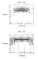
- FIG. 3shows the light-current curves for an exemplary 2.4 ⁇ m and 10 ⁇ m waveguide.
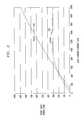
- FIGS. 4A-4Bdepict horizontal and vertical far-field patterns of an exemplary 10 ⁇ m width waveguide laser.
- FIG. 1depicts a heterostructure laser 100 .
- the active region 102has blocking 160 regions 104 adjacent thereto and extending laterally from opposite sides of active region 102 .
- Blocking regions 104may consist of a plurality of layers.
- the refractive index of the active region materialdiffers from that of the blocking region material providing lateral optical confinement. The difference in refractive indices also provides the current blocking capability useful in limiting the laser drive current from leaking through the non-active region.
- the effective refractive index difference between the blocking region and the fundamental transverse mode of the active regionis about 0.03. This provides a single transverse mode for a 1480 nm pump laser with an active region stripe width of 2.4 ⁇ cm.
- the stripe widthWhen the stripe width is increased an unwanted second transverse mode may arise.
- the transverse electrical (TE) mode with lowest lossis the TE 06 .
- a 10 ⁇ m stripe widthmay be easily coupled to optical fibers having that width which are readily available.
- the blocking regions and active regionmay be comprised of like-materials.
- InGaAsPmay be used both as blocking and active region materials.
- like-materialsmeans materials comprised of the same elements but differing in the ratio of elements. Reference to a particular material includes that material in a pure form or having impurities or dopants. The use of like-materials reduces the refractive index difference between the active and blocking regions such that the TE 00 mode may spread over a larger width as compared, for example, to a heterojunction comprising conventional InP blocking regions and an InGaAsP active region.
- use of like-materials for the blocking regionsalso avoids significant lattice mismatch at the heterojunction of the active and blocking regions.
- Lattice mismatch between materials making up the heterojunctionmay result in lattice defects. These defects may reduce radiative recombination efficiency thereby reducing the device life expectancy.
- use of like-materials for the active and blocking regionsmay improve device quality and performance.
- FIGS. 2A-Cprovide TE modes with lowest loss for different blocking material refractive indices.
- the TE modes depicted in FIGS. 2A-2Care produced by blocking materials having refractive indices of 3.160, 3.180, and 3.190, respectively.
- the blocking material having a refractive index of 3.180provides a fundamental transverse mode. This represents a refractive index difference between the active and blocking regions of 0.023.
- 0.95 Ga 0.05 As 0.12 P 0.88is an example of a material having this refractive index.
- the bandgap energy for the materialis 1.267 eV with a corresponding wavelength of 0.979 ⁇ m.
- the bandgap energyis only 0.083 eV smaller than that of InP, and thus, should not degrade the blocking characteristics of the p-n junctions.
- Single-mode rate equationswere used to simulate light-current (LI) characteristics of the larger stripe width obtained with the InGaAsP material having a 3.180 refractive index.
- the LI curve of a conventional high performance 1480 nm pump laserwas modeled.
- the simulated internal power lossis 12.5 cm ⁇ 1 and the confinement factor is 5.87%.
- the threshold currentis 26 mA
- the front facet power at 600 mAis 241 mW
- the roll-over currentis 1200 mA, for a chip length of 1 mm.
- a simulationwas performed using an internal loss of 11.7 cm ⁇ 1 and a confinement factor of 6.18%.
- FIG. 3shows the LI curves 302 and 304 for the 2.4 ⁇ m waveguide width and the 10 ⁇ m waveguide width, respectively.
- FIGS. 4A-BA simulation was also produced for both horizontal (x) and vertical (y) far-field patterns of the 10 ⁇ m width waveguide laser. These patterns are depicted in FIGS. 4A-B, respectively.
- the horizontal full-width-half-maximum (FWHM) far-field anglewas 7.6 degrees and the vertical angle was 31.5 degrees.
- this beam patternis ideal for coupling to a cylindrical fiber lens and may provide a coupling efficiency of greater than 80%.
- a fiber coupled power of greater than 500 mWmay be realized at 1500 mA.
- the thermal power dissipationmay be 1.74 W at a laser driving current of 1500 mA, making it possible to package the device with a standard 14 pin butterfly enclosure.
- the simulationsprovided a basis for a design of the semiconductor pump laser having an active region material and a blocking region material wherein the refractive index difference between the two materials at the fundamental frequency is less than about 0.029 and wherein the laser has a single transverse mode.
- An exemplary refractive index difference range for the semiconductor laseris about 0.020 to 0.025. It is desirable that the index of refraction of the active region material is greater than the refractive index of the blocking region material.
- the blocking region materialis In 0.95 Ga 0.05 As 0.12 P 0.88 . More generally the blocking material may, for example, comprise In 1-x Ga x As y P 1-y wherein x is less than about 0.96 and y is less than about 0.90.
- the active region materialis GaAs and the blocking region material is InGaAsP. The composition of InGaAsP may be chosen to obtain the desired refractive index difference between the active and blocking regions.
- the active region width of the lasermay be greater than about 2.4 ⁇ m with exemplary ranges of about 3.0 ⁇ m to 15 ⁇ m, and about 8.5 ⁇ m to 10.5 ⁇ m.
- the laserhas a refractive index difference between the active and blocking regions of about 0.020 to 0.025 and an active region width in the range of about 8.5 ⁇ m to 10.5 ⁇ m.
- Embodiments of the inventionprovide a front facet power greater than or equal to about 500 mW with an illustrative range of 500 mW to 900 mW.
- a particular embodiment of the inventionprovides a laser with an active region having a width in the range of about 8 ⁇ m to 11 ⁇ m and having a front facet power in the range of about 700 mW to 800 mW.
- the single mode transmission power of the laseris greater than about 300 mW, with an exemplary range of about 300 mW to about 550 mW.
- blocking regionscomprise a stack of at least one n-InGaAsP, p-InGaAsP pair, wherein an n-InGaAsP layer is adjacent to a p-electrode and a p-InGaAsP layer is adjacent to an n-electrode.
- the blocking regionsmay also be constructed with a semi-insulating layer.
- An illustrative exampleincludes a semi-insulating layer between a p-InP layer and an n-InP layer.
- the refractive index differences described abovemay achieve confinement factors of greater than about 6.0%, with an illustrative range of about 6% to 7%.
- Embodiments of the inventionmay be applied to lasers of any wavelength but present technology will likely encourage use with lasers having wavelengths of 1480 nm and 980 nm for example.
- Blocking capabilitygenerally increases as the blocking material bandgap energy increases.
- the blocking materialmay have, for example, a bandgap energy greater than 1.20 eV, with an illustrative range of about 1.20 eV to 1.40 eV.
- Semiconductor laser 100is fabricated by first providing substrate 106 which has an illustrative thickness in the range of about 50 ⁇ m to 150 ⁇ m with an exemplary thickness of 100 ⁇ m.
- Active region 102 and blocking regions 104are disposed on substrate 106 and have a refractive index difference of less than about 0.029. In one embodiment of the invention the desired refractive index difference is achieved by forming the active and blocking regions of like-materials.
- Active region 102may have, for example, a thickness in the range of about 0.041 ⁇ m to 0.06 ⁇ cm, and is disposed between blocking regions 104 .
- Top layer 108is disposed on blocking regions 104 and active region 102 , and may have, for example, a thickness in the range of about 2 ⁇ m to 4 ⁇ m with an illustrative thickness of about 3 ⁇ m.
- Blocking regions 104comprise a plurality of layers which may have thicknesses in a range of about 0.5 ⁇ m to 1.5 ⁇ m, with a demonstrative thickness of 1.0 ⁇ m.
- Electrodes(not shown) are provided above top layer 108 and below substrate 106 and may have thicknesses in the range of about 3.5 ⁇ m to 4.5 ⁇ m.
- Embodiments of the inventionprovide an active area having a high coupling efficiency to an optical fiber as compared to conventional lasers.
- the coupling efficiency to a single mode fibermay be greater than about 75%.
- Embodiments of the inventionare particularly applicable to fiber amplifiers, for example, erbium doped fiber amplifiers and Raman fiber amplifiers.
- the laser of the present inventionmay be fabricated by any conventional method by which active and blocking regions may be formed wherein their refractive index difference at the fundamental frequency is less than about 0.029.
- a fabrication method for a mesa buried heterostructure distributed feedback laserwhich may be used to construct a laser according to embodiments of the present invention.
- a double heterostructureis grown over conventional first-order distributed feedback gratings that are etched into a substrate.
- the substratemay be, for example, InP.
- the double heterostructuremay be grown by a variety of epitaxial techniques such as for example, liquid phase epitaxy, hybrid vapor phase epitaxy, and metalorganic vapor phase epitaxy.
- the double heterostructuremay consist of a plurality of layers.
- An oxide layer, such as silicon dioxide for example,is deposited over the surface of the double heterostructure. Stripes are photolithographically patterned in a direction perpendicular to the gratings.
- the silicon dioxide, or analogous layerserves as both an etch mask during mesa etching and a growth mask during blocking layer growth which is performed using metalorganic vapor phase epitaxy.
- Mesasare chemically etched to the desired width, for example, 1.0-3.0 ⁇ m.
- the mesas that are formedare vertical walled for several microns below the surface, thus providing good correspondence between the mesa width and the active width.
- semi-insulating blocking layersare regrown around the mesas by selective metalorganic vapor phase epitaxy.
- the SiO 2is etched away in HF, and hybrid vapor phase epitaxy is used to provide additional thickness to the double heterostructure.
- the wafersare processed using conventional n- and p- contacts. The wafers are thinned and the laser chips cleaved and bonded to copper or ceramic sinks.
- Asymmetric high reflectivity anti-reflection mirror coatingsare applied to the facets by electron beam evaporation to stabilize the single-longitudinal mode.
- the anti-reflection coatingconsists of amorphous zirconia with 10% yttria and the asymmetric high reflectivity coating is yttria which is overcoated with silicon.
Landscapes
- Physics & Mathematics (AREA)
- Geometry (AREA)
- Condensed Matter Physics & Semiconductors (AREA)
- General Physics & Mathematics (AREA)
- Electromagnetism (AREA)
- Optics & Photonics (AREA)
- Semiconductor Lasers (AREA)
Abstract
Description
Claims (16)
Priority Applications (5)
| Application Number | Priority Date | Filing Date | Title |
|---|---|---|---|
| US09/602,931US6432735B1 (en) | 2000-06-23 | 2000-06-23 | High power single mode laser and method of fabrication |
| DE60107494TDE60107494T2 (en) | 2000-06-23 | 2001-06-13 | High performance single mode laser and manufacturing process |
| EP01401531AEP1168541B1 (en) | 2000-06-23 | 2001-06-13 | High power single mode laser and method of fabrication |
| JP2001189194AJP2002057409A (en) | 2000-06-23 | 2001-06-22 | Semiconductor laser and its fabricating method |
| US10/165,825US6552358B2 (en) | 2000-06-23 | 2002-06-08 | High power single mode laser and method of fabrication |
Applications Claiming Priority (1)
| Application Number | Priority Date | Filing Date | Title |
|---|---|---|---|
| US09/602,931US6432735B1 (en) | 2000-06-23 | 2000-06-23 | High power single mode laser and method of fabrication |
Related Child Applications (1)
| Application Number | Title | Priority Date | Filing Date |
|---|---|---|---|
| US10/165,825DivisionUS6552358B2 (en) | 2000-06-23 | 2002-06-08 | High power single mode laser and method of fabrication |
Publications (1)
| Publication Number | Publication Date |
|---|---|
| US6432735B1true US6432735B1 (en) | 2002-08-13 |
Family
ID=24413344
Family Applications (2)
| Application Number | Title | Priority Date | Filing Date |
|---|---|---|---|
| US09/602,931Expired - LifetimeUS6432735B1 (en) | 2000-06-23 | 2000-06-23 | High power single mode laser and method of fabrication |
| US10/165,825Expired - Fee RelatedUS6552358B2 (en) | 2000-06-23 | 2002-06-08 | High power single mode laser and method of fabrication |
Family Applications After (1)
| Application Number | Title | Priority Date | Filing Date |
|---|---|---|---|
| US10/165,825Expired - Fee RelatedUS6552358B2 (en) | 2000-06-23 | 2002-06-08 | High power single mode laser and method of fabrication |
Country Status (4)
| Country | Link |
|---|---|
| US (2) | US6432735B1 (en) |
| EP (1) | EP1168541B1 (en) |
| JP (1) | JP2002057409A (en) |
| DE (1) | DE60107494T2 (en) |
Cited By (4)
| Publication number | Priority date | Publication date | Assignee | Title |
|---|---|---|---|---|
| US20040086017A1 (en)* | 2002-02-19 | 2004-05-06 | The Furukawa Electric Co., Ltd. | Semiconductor laser device and semiconductor laser module |
| US20040147094A1 (en)* | 2002-12-20 | 2004-07-29 | Haberern Kevin Ward | Methods of forming semiconductor devices having self aligned semiconductor mesas and contact layers and related devices |
| US20110128982A1 (en)* | 2009-12-02 | 2011-06-02 | Huang Robin K | High efficiency slab-coupled optical waveguide laser and amplifier |
| US20110150010A1 (en)* | 2009-12-02 | 2011-06-23 | Huang Robin K | Very large mode slab-coupled optical waveguide laser and amplifier |
Families Citing this family (4)
| Publication number | Priority date | Publication date | Assignee | Title |
|---|---|---|---|---|
| US6829275B2 (en)* | 2001-12-20 | 2004-12-07 | Bookham Technology, Plc | Hybrid confinement layers of buried heterostructure semiconductor laser |
| JP2005302910A (en)* | 2004-04-09 | 2005-10-27 | Fujitsu Ltd | Semiconductor light emitting device |
| US7949031B2 (en)* | 2006-06-16 | 2011-05-24 | Pbc Lasers Gmbh | Optoelectronic systems providing high-power high-brightness laser light based on field coupled arrays, bars and stacks of semicondutor diode lasers |
| KR102747154B1 (en)* | 2018-04-18 | 2024-12-31 | 사우디 아람코 테크놀로지스 컴퍼니 | Terminal group isomerization of poly(alkylene carbonate) polymers |
Citations (1)
| Publication number | Priority date | Publication date | Assignee | Title |
|---|---|---|---|---|
| US5583881A (en)* | 1994-02-10 | 1996-12-10 | Rohm Co., Ltd. | Semiconductor laser and method for manufacturing the same |
Family Cites Families (9)
| Publication number | Priority date | Publication date | Assignee | Title |
|---|---|---|---|---|
| JPS5769791A (en)* | 1980-10-17 | 1982-04-28 | Nec Corp | Buried heterostructural semiconductor laser device having low radiation angle and manufacture thereof |
| JPS6273687A (en)* | 1985-09-26 | 1987-04-04 | Mitsubishi Electric Corp | semiconductor laser equipment |
| JPS6373683A (en)* | 1986-09-17 | 1988-04-04 | Furukawa Electric Co Ltd:The | Distributed feedback semiconductor laser |
| US4875216A (en)* | 1987-11-30 | 1989-10-17 | Xerox Corporation | Buried waveguide window regions for improved performance semiconductor lasers and other opto-electronic applications |
| JPH02159784A (en)* | 1988-12-14 | 1990-06-19 | Oki Electric Ind Co Ltd | Semiconductor laser |
| JPH065975A (en)* | 1992-06-22 | 1994-01-14 | Matsushita Electric Ind Co Ltd | Semiconductor laser |
| TW342545B (en)* | 1996-03-28 | 1998-10-11 | Sanyo Electric Co | Semiconductor laser element and method for designing same |
| JPH10150244A (en)* | 1996-11-20 | 1998-06-02 | Mitsubishi Electric Corp | Semiconductor device simulation method |
| JP3859839B2 (en)* | 1997-09-30 | 2006-12-20 | 富士フイルムホールディングス株式会社 | Refractive index semiconductor laser device |
- 2000
- 2000-06-23USUS09/602,931patent/US6432735B1/ennot_activeExpired - Lifetime
- 2001
- 2001-06-13EPEP01401531Apatent/EP1168541B1/ennot_activeExpired - Lifetime
- 2001-06-13DEDE60107494Tpatent/DE60107494T2/ennot_activeExpired - Lifetime
- 2001-06-22JPJP2001189194Apatent/JP2002057409A/enactivePending
- 2002
- 2002-06-08USUS10/165,825patent/US6552358B2/ennot_activeExpired - Fee Related
Patent Citations (1)
| Publication number | Priority date | Publication date | Assignee | Title |
|---|---|---|---|---|
| US5583881A (en)* | 1994-02-10 | 1996-12-10 | Rohm Co., Ltd. | Semiconductor laser and method for manufacturing the same |
Non-Patent Citations (1)
| Title |
|---|
| Growth and Characterization of High Yield, Reliable High Power, High Speed, InP/InGaAsP Capped Mesa Buried Heterostructure Distributed Feedback (CMBH-DFB) Lasers, Zilko, et al, IEEE Journal of Quantum Electronics, vol. 25, No. 10, Oct. 1989. |
Cited By (10)
| Publication number | Priority date | Publication date | Assignee | Title |
|---|---|---|---|---|
| US20040086017A1 (en)* | 2002-02-19 | 2004-05-06 | The Furukawa Electric Co., Ltd. | Semiconductor laser device and semiconductor laser module |
| US6996149B2 (en) | 2002-02-19 | 2006-02-07 | The Furukawa Electric Co., Ltd. | Semiconductor laser device and semiconductor laser module |
| US20040147094A1 (en)* | 2002-12-20 | 2004-07-29 | Haberern Kevin Ward | Methods of forming semiconductor devices having self aligned semiconductor mesas and contact layers and related devices |
| US7160747B2 (en)* | 2002-12-20 | 2007-01-09 | Cree, Inc. | Methods of forming semiconductor devices having self aligned semiconductor mesas and contact layers |
| US20070007544A1 (en)* | 2002-12-20 | 2007-01-11 | Haberern Kevin W | Semiconductor devices having self aligned semiconductor mesas and contact layers |
| US7613219B2 (en) | 2002-12-20 | 2009-11-03 | Cree, Inc. | Semiconductor devices having self aligned semiconductor mesas and contact layers |
| US20110128982A1 (en)* | 2009-12-02 | 2011-06-02 | Huang Robin K | High efficiency slab-coupled optical waveguide laser and amplifier |
| US20110150010A1 (en)* | 2009-12-02 | 2011-06-23 | Huang Robin K | Very large mode slab-coupled optical waveguide laser and amplifier |
| US8451874B2 (en)* | 2009-12-02 | 2013-05-28 | Massachusetts Institute Of Technology | Very large mode slab-coupled optical waveguide laser and amplifier |
| US8571080B2 (en) | 2009-12-02 | 2013-10-29 | Massachusetts Institute Of Technology | High efficiency slab-coupled optical waveguide laser and amplifier |
Also Published As
| Publication number | Publication date |
|---|---|
| EP1168541B1 (en) | 2004-12-01 |
| US20030017662A1 (en) | 2003-01-23 |
| US6552358B2 (en) | 2003-04-22 |
| DE60107494T2 (en) | 2005-12-08 |
| EP1168541A3 (en) | 2003-03-26 |
| DE60107494D1 (en) | 2005-01-05 |
| EP1168541A2 (en) | 2002-01-02 |
| JP2002057409A (en) | 2002-02-22 |
Similar Documents
| Publication | Publication Date | Title |
|---|---|---|
| US6426515B2 (en) | Semiconductor light-emitting device | |
| US6815786B2 (en) | Semiconductor optical device and method of manufacturing the same | |
| US6162655A (en) | Method of fabricating an expanded beam optical waveguide device | |
| US20040179569A1 (en) | Wavelength tunable DBR laser diode | |
| US8179592B2 (en) | Semiconductor optical amplifier, method for manufacturing the same, and semiconductor optical integrated device | |
| US5636237A (en) | Semiconductor laser device which makes it possible to realize high-speed modulation | |
| JP5314435B2 (en) | Integrated optical device and manufacturing method thereof | |
| US7454111B2 (en) | Optical device of waveguide type and its production method | |
| US6678302B2 (en) | Semiconductor device and manufacturing method thereof | |
| CN107565381A (en) | Distributed feedback type semiconductor laser device and integreted phontonics transmitting chip module | |
| EP1416598A2 (en) | Semiconductor light emitting device in which high-power light output can be obtained with a simple structure | |
| US6432735B1 (en) | High power single mode laser and method of fabrication | |
| US20090267195A1 (en) | Semiconductor element and method for manufacturing semiconductor element | |
| US20230021415A1 (en) | Manufacturing Method for Semiconductor Device | |
| CN116207608A (en) | Quantum dot laser structure and preparation method thereof | |
| US20030047738A1 (en) | Semiconductor laser device having selective absorption qualities over a wide temperature range | |
| US20050185689A1 (en) | Optoelectronic device having a Discrete Bragg Reflector and an electro-absorption modulator | |
| JP2882335B2 (en) | Optical semiconductor device and method for manufacturing the same | |
| JPH11204773A (en) | Waveguide-type semiconductor optical integrated device and method of manufacturing the same | |
| Bornholdt et al. | Passive optical GaInAsP/InP waveguides | |
| JP3241002B2 (en) | Manufacturing method of semiconductor laser | |
| JP2002026461A (en) | Optical semiconductor device, method of manufacturing the same, optical device module including optical semiconductor device, and optical communication device | |
| Ryu et al. | 1.55-μm spot-size converter integrated laser diode with conventional buried-heterostructure laser process | |
| JP4164248B2 (en) | Semiconductor element, manufacturing method thereof, and semiconductor optical device | |
| JPH10233551A (en) | Semiconductor light emitting device |
Legal Events
| Date | Code | Title | Description |
|---|---|---|---|
| AS | Assignment | Owner name:LUCENT TECHNOLOGIES, INC., NEW JERSEY Free format text:ASSIGNMENT OF ASSIGNORS INTEREST;ASSIGNORS:CHO, SI HYUNG;DAUTREMONT-SMITH, WILLIAM C.;HUANG, SUN YUAN;REEL/FRAME:011176/0776;SIGNING DATES FROM 20000814 TO 20000905 | |
| STCF | Information on status: patent grant | Free format text:PATENTED CASE | |
| FEPP | Fee payment procedure | Free format text:PAYOR NUMBER ASSIGNED (ORIGINAL EVENT CODE: ASPN); ENTITY STATUS OF PATENT OWNER: LARGE ENTITY | |
| FPAY | Fee payment | Year of fee payment:4 | |
| FPAY | Fee payment | Year of fee payment:8 | |
| FPAY | Fee payment | Year of fee payment:12 | |
| AS | Assignment | Owner name:DEUTSCHE BANK AG NEW YORK BRANCH, AS COLLATERAL AG Free format text:PATENT SECURITY AGREEMENT;ASSIGNORS:LSI CORPORATION;AGERE SYSTEMS LLC;REEL/FRAME:032856/0031 Effective date:20140506 | |
| AS | Assignment | Owner name:AVAGO TECHNOLOGIES GENERAL IP (SINGAPORE) PTE. LTD Free format text:ASSIGNMENT OF ASSIGNORS INTEREST;ASSIGNOR:AGERE SYSTEMS LLC;REEL/FRAME:035365/0634 Effective date:20140804 | |
| AS | Assignment | Owner name:LSI CORPORATION, CALIFORNIA Free format text:TERMINATION AND RELEASE OF SECURITY INTEREST IN PATENT RIGHTS (RELEASES RF 032856-0031);ASSIGNOR:DEUTSCHE BANK AG NEW YORK BRANCH, AS COLLATERAL AGENT;REEL/FRAME:037684/0039 Effective date:20160201 Owner name:AGERE SYSTEMS LLC, PENNSYLVANIA Free format text:TERMINATION AND RELEASE OF SECURITY INTEREST IN PATENT RIGHTS (RELEASES RF 032856-0031);ASSIGNOR:DEUTSCHE BANK AG NEW YORK BRANCH, AS COLLATERAL AGENT;REEL/FRAME:037684/0039 Effective date:20160201 | |
| AS | Assignment | Owner name:BANK OF AMERICA, N.A., AS COLLATERAL AGENT, NORTH CAROLINA Free format text:PATENT SECURITY AGREEMENT;ASSIGNOR:AVAGO TECHNOLOGIES GENERAL IP (SINGAPORE) PTE. LTD.;REEL/FRAME:037808/0001 Effective date:20160201 Owner name:BANK OF AMERICA, N.A., AS COLLATERAL AGENT, NORTH Free format text:PATENT SECURITY AGREEMENT;ASSIGNOR:AVAGO TECHNOLOGIES GENERAL IP (SINGAPORE) PTE. LTD.;REEL/FRAME:037808/0001 Effective date:20160201 | |
| AS | Assignment | Owner name:AVAGO TECHNOLOGIES GENERAL IP (SINGAPORE) PTE. LTD., SINGAPORE Free format text:TERMINATION AND RELEASE OF SECURITY INTEREST IN PATENTS;ASSIGNOR:BANK OF AMERICA, N.A., AS COLLATERAL AGENT;REEL/FRAME:041710/0001 Effective date:20170119 Owner name:AVAGO TECHNOLOGIES GENERAL IP (SINGAPORE) PTE. LTD Free format text:TERMINATION AND RELEASE OF SECURITY INTEREST IN PATENTS;ASSIGNOR:BANK OF AMERICA, N.A., AS COLLATERAL AGENT;REEL/FRAME:041710/0001 Effective date:20170119 | |
| AS | Assignment | Owner name:AVAGO TECHNOLOGIES INTERNATIONAL SALES PTE. LIMITE Free format text:MERGER;ASSIGNOR:AVAGO TECHNOLOGIES GENERAL IP (SINGAPORE) PTE. LTD.;REEL/FRAME:047195/0026 Effective date:20180509 | |
| AS | Assignment | Owner name:AVAGO TECHNOLOGIES INTERNATIONAL SALES PTE. LIMITE Free format text:CORRECTIVE ASSIGNMENT TO CORRECT THE EFFECTIVE DATE OF MERGER PREVIOUSLY RECORDED ON REEL 047195 FRAME 0026. ASSIGNOR(S) HEREBY CONFIRMS THE MERGER;ASSIGNOR:AVAGO TECHNOLOGIES GENERAL IP (SINGAPORE) PTE. LTD.;REEL/FRAME:047477/0423 Effective date:20180905 |