US6431952B2 - Apparatus and methods for substantial planarization of solder bumps - Google Patents
Apparatus and methods for substantial planarization of solder bumpsDownload PDFInfo
- Publication number
- US6431952B2 US6431952B2US09/900,330US90033001AUS6431952B2US 6431952 B2US6431952 B2US 6431952B2US 90033001 AUS90033001 AUS 90033001AUS 6431952 B2US6431952 B2US 6431952B2
- Authority
- US
- United States
- Prior art keywords
- planarization
- solder bumps
- outer surfaces
- bumped device
- bumped
- Prior art date
- Legal status (The legal status is an assumption and is not a legal conclusion. Google has not performed a legal analysis and makes no representation as to the accuracy of the status listed.)
- Expired - Lifetime
Links
- 229910000679solderInorganic materials0.000titleclaimsabstractdescription163
- 238000000034methodMethods0.000titleabstractdescription17
- 230000009471actionEffects0.000claimsabstractdescription38
- 238000012544monitoring processMethods0.000claims2
- 230000008021depositionEffects0.000abstractdescription13
- 230000008569processEffects0.000abstractdescription9
- 238000000227grindingMethods0.000abstractdescription7
- 238000003801millingMethods0.000abstractdescription4
- 239000000126substanceSubstances0.000abstractdescription4
- 239000000654additiveSubstances0.000abstractdescription3
- 230000000996additive effectEffects0.000abstractdescription3
- 230000000930thermomechanical effectEffects0.000abstractdescription3
- 238000006243chemical reactionMethods0.000abstractdescription2
- 238000012360testing methodMethods0.000description18
- 230000006835compressionEffects0.000description10
- 238000007906compressionMethods0.000description10
- 239000011241protective layerSubstances0.000description10
- 238000004519manufacturing processMethods0.000description9
- 230000008901benefitEffects0.000description6
- 230000002829reductive effectEffects0.000description6
- 239000010410layerSubstances0.000description5
- 235000012431wafersNutrition0.000description5
- 239000000463materialSubstances0.000description4
- 238000004806packaging method and processMethods0.000description4
- 230000007246mechanismEffects0.000description3
- 238000005498polishingMethods0.000description3
- GRYLNZFGIOXLOG-UHFFFAOYSA-NNitric acidChemical compoundO[N+]([O-])=OGRYLNZFGIOXLOG-UHFFFAOYSA-N0.000description2
- 230000003247decreasing effectEffects0.000description2
- VCJMYUPGQJHHFU-UHFFFAOYSA-Niron(3+);trinitrateChemical compound[Fe+3].[O-][N+]([O-])=O.[O-][N+]([O-])=O.[O-][N+]([O-])=OVCJMYUPGQJHHFU-UHFFFAOYSA-N0.000description2
- NJPPVKZQTLUDBO-UHFFFAOYSA-NnovaluronChemical compoundC1=C(Cl)C(OC(F)(F)C(OC(F)(F)F)F)=CC=C1NC(=O)NC(=O)C1=C(F)C=CC=C1FNJPPVKZQTLUDBO-UHFFFAOYSA-N0.000description2
- 230000036961partial effectEffects0.000description2
- 239000000758substrateSubstances0.000description2
- MIMUSZHMZBJBPO-UHFFFAOYSA-N6-methoxy-8-nitroquinolineChemical compoundN1=CC=CC2=CC(OC)=CC([N+]([O-])=O)=C21MIMUSZHMZBJBPO-UHFFFAOYSA-N0.000description1
- 229910021578Iron(III) chlorideInorganic materials0.000description1
- XUIMIQQOPSSXEZ-UHFFFAOYSA-NSiliconChemical compound[Si]XUIMIQQOPSSXEZ-UHFFFAOYSA-N0.000description1
- 230000001133accelerationEffects0.000description1
- 239000002253acidSubstances0.000description1
- 238000013459approachMethods0.000description1
- 238000003491arrayMethods0.000description1
- 239000011248coating agentSubstances0.000description1
- 238000000576coating methodMethods0.000description1
- 238000005137deposition processMethods0.000description1
- 238000011161developmentMethods0.000description1
- 238000005530etchingMethods0.000description1
- 238000010438heat treatmentMethods0.000description1
- KRHYYFGTRYWZRS-UHFFFAOYSA-Nhydrofluoric acidSubstancesFKRHYYFGTRYWZRS-UHFFFAOYSA-N0.000description1
- 238000009434installationMethods0.000description1
- RBTARNINKXHZNM-UHFFFAOYSA-Kiron trichlorideChemical compoundCl[Fe](Cl)ClRBTARNINKXHZNM-UHFFFAOYSA-K0.000description1
- 239000007788liquidSubstances0.000description1
- 238000012423maintenanceMethods0.000description1
- 238000004377microelectronicMethods0.000description1
- 238000012986modificationMethods0.000description1
- 230000004048modificationEffects0.000description1
- QPJSUIGXIBEQAC-UHFFFAOYSA-Nn-(2,4-dichloro-5-propan-2-yloxyphenyl)acetamideChemical compoundCC(C)OC1=CC(NC(C)=O)=C(Cl)C=C1ClQPJSUIGXIBEQAC-UHFFFAOYSA-N0.000description1
- 229910017604nitric acidInorganic materials0.000description1
- 230000003287optical effectEffects0.000description1
- 238000012536packaging technologyMethods0.000description1
- 150000002978peroxidesChemical class0.000description1
- 230000008439repair processEffects0.000description1
- 230000000284resting effectEffects0.000description1
- 238000012552reviewMethods0.000description1
- 239000004065semiconductorSubstances0.000description1
- 229910052710siliconInorganic materials0.000description1
- 239000010703siliconSubstances0.000description1
- 239000002002slurrySubstances0.000description1
- 238000009736wettingMethods0.000description1
Images


Classifications
- H—ELECTRICITY
- H05—ELECTRIC TECHNIQUES NOT OTHERWISE PROVIDED FOR
- H05K—PRINTED CIRCUITS; CASINGS OR CONSTRUCTIONAL DETAILS OF ELECTRIC APPARATUS; MANUFACTURE OF ASSEMBLAGES OF ELECTRICAL COMPONENTS
- H05K3/00—Apparatus or processes for manufacturing printed circuits
- H05K3/30—Assembling printed circuits with electric components, e.g. with resistor
- H05K3/32—Assembling printed circuits with electric components, e.g. with resistor electrically connecting electric components or wires to printed circuits
- H05K3/34—Assembling printed circuits with electric components, e.g. with resistor electrically connecting electric components or wires to printed circuits by soldering
- H05K3/3457—Solder materials or compositions; Methods of application thereof
- B—PERFORMING OPERATIONS; TRANSPORTING
- B24—GRINDING; POLISHING
- B24B—MACHINES, DEVICES, OR PROCESSES FOR GRINDING OR POLISHING; DRESSING OR CONDITIONING OF ABRADING SURFACES; FEEDING OF GRINDING, POLISHING, OR LAPPING AGENTS
- B24B37/00—Lapping machines or devices; Accessories
- B24B37/04—Lapping machines or devices; Accessories designed for working plane surfaces
- B24B37/042—Lapping machines or devices; Accessories designed for working plane surfaces operating processes therefor
- B—PERFORMING OPERATIONS; TRANSPORTING
- B24—GRINDING; POLISHING
- B24B—MACHINES, DEVICES, OR PROCESSES FOR GRINDING OR POLISHING; DRESSING OR CONDITIONING OF ABRADING SURFACES; FEEDING OF GRINDING, POLISHING, OR LAPPING AGENTS
- B24B7/00—Machines or devices designed for grinding plane surfaces on work, including polishing plane glass surfaces; Accessories therefor
- B24B7/20—Machines or devices designed for grinding plane surfaces on work, including polishing plane glass surfaces; Accessories therefor characterised by a special design with respect to properties of the material of non-metallic articles to be ground
- B24B7/22—Machines or devices designed for grinding plane surfaces on work, including polishing plane glass surfaces; Accessories therefor characterised by a special design with respect to properties of the material of non-metallic articles to be ground for grinding inorganic material, e.g. stone, ceramics, porcelain
- H—ELECTRICITY
- H01—ELECTRIC ELEMENTS
- H01L—SEMICONDUCTOR DEVICES NOT COVERED BY CLASS H10
- H01L21/00—Processes or apparatus adapted for the manufacture or treatment of semiconductor or solid state devices or of parts thereof
- H01L21/02—Manufacture or treatment of semiconductor devices or of parts thereof
- H01L21/04—Manufacture or treatment of semiconductor devices or of parts thereof the devices having potential barriers, e.g. a PN junction, depletion layer or carrier concentration layer
- H01L21/48—Manufacture or treatment of parts, e.g. containers, prior to assembly of the devices, using processes not provided for in a single one of the groups H01L21/18 - H01L21/326 or H10D48/04 - H10D48/07
- H01L21/4814—Conductive parts
- H01L21/4846—Leads on or in insulating or insulated substrates, e.g. metallisation
- H01L21/4853—Connection or disconnection of other leads to or from a metallisation, e.g. pins, wires, bumps
- H—ELECTRICITY
- H01—ELECTRIC ELEMENTS
- H01L—SEMICONDUCTOR DEVICES NOT COVERED BY CLASS H10
- H01L24/00—Arrangements for connecting or disconnecting semiconductor or solid-state bodies; Methods or apparatus related thereto
- H01L24/01—Means for bonding being attached to, or being formed on, the surface to be connected, e.g. chip-to-package, die-attach, "first-level" interconnects; Manufacturing methods related thereto
- H01L24/10—Bump connectors ; Manufacturing methods related thereto
- H01L24/11—Manufacturing methods
- H—ELECTRICITY
- H01—ELECTRIC ELEMENTS
- H01L—SEMICONDUCTOR DEVICES NOT COVERED BY CLASS H10
- H01L22/00—Testing or measuring during manufacture or treatment; Reliability measurements, i.e. testing of parts without further processing to modify the parts as such; Structural arrangements therefor
- H01L22/10—Measuring as part of the manufacturing process
- H01L22/12—Measuring as part of the manufacturing process for structural parameters, e.g. thickness, line width, refractive index, temperature, warp, bond strength, defects, optical inspection, electrical measurement of structural dimensions, metallurgic measurement of diffusions
- H—ELECTRICITY
- H01—ELECTRIC ELEMENTS
- H01L—SEMICONDUCTOR DEVICES NOT COVERED BY CLASS H10
- H01L2224/00—Indexing scheme for arrangements for connecting or disconnecting semiconductor or solid-state bodies and methods related thereto as covered by H01L24/00
- H01L2224/01—Means for bonding being attached to, or being formed on, the surface to be connected, e.g. chip-to-package, die-attach, "first-level" interconnects; Manufacturing methods related thereto
- H01L2224/02—Bonding areas; Manufacturing methods related thereto
- H01L2224/04—Structure, shape, material or disposition of the bonding areas prior to the connecting process
- H01L2224/0401—Bonding areas specifically adapted for bump connectors, e.g. under bump metallisation [UBM]
- H—ELECTRICITY
- H01—ELECTRIC ELEMENTS
- H01L—SEMICONDUCTOR DEVICES NOT COVERED BY CLASS H10
- H01L2224/00—Indexing scheme for arrangements for connecting or disconnecting semiconductor or solid-state bodies and methods related thereto as covered by H01L24/00
- H01L2224/01—Means for bonding being attached to, or being formed on, the surface to be connected, e.g. chip-to-package, die-attach, "first-level" interconnects; Manufacturing methods related thereto
- H01L2224/02—Bonding areas; Manufacturing methods related thereto
- H01L2224/04—Structure, shape, material or disposition of the bonding areas prior to the connecting process
- H01L2224/06—Structure, shape, material or disposition of the bonding areas prior to the connecting process of a plurality of bonding areas
- H01L2224/0601—Structure
- H01L2224/0603—Bonding areas having different sizes, e.g. different heights or widths
- H—ELECTRICITY
- H01—ELECTRIC ELEMENTS
- H01L—SEMICONDUCTOR DEVICES NOT COVERED BY CLASS H10
- H01L2224/00—Indexing scheme for arrangements for connecting or disconnecting semiconductor or solid-state bodies and methods related thereto as covered by H01L24/00
- H01L2224/01—Means for bonding being attached to, or being formed on, the surface to be connected, e.g. chip-to-package, die-attach, "first-level" interconnects; Manufacturing methods related thereto
- H01L2224/10—Bump connectors; Manufacturing methods related thereto
- H01L2224/11—Manufacturing methods
- H01L2224/118—Post-treatment of the bump connector
- H01L2224/1183—Reworking, e.g. shaping
- H01L2224/1184—Reworking, e.g. shaping involving a mechanical process, e.g. planarising the bump connector
- H—ELECTRICITY
- H01—ELECTRIC ELEMENTS
- H01L—SEMICONDUCTOR DEVICES NOT COVERED BY CLASS H10
- H01L2224/00—Indexing scheme for arrangements for connecting or disconnecting semiconductor or solid-state bodies and methods related thereto as covered by H01L24/00
- H01L2224/01—Means for bonding being attached to, or being formed on, the surface to be connected, e.g. chip-to-package, die-attach, "first-level" interconnects; Manufacturing methods related thereto
- H01L2224/10—Bump connectors; Manufacturing methods related thereto
- H01L2224/12—Structure, shape, material or disposition of the bump connectors prior to the connecting process
- H01L2224/13—Structure, shape, material or disposition of the bump connectors prior to the connecting process of an individual bump connector
- H01L2224/13001—Core members of the bump connector
- H01L2224/13099—Material
- H—ELECTRICITY
- H01—ELECTRIC ELEMENTS
- H01L—SEMICONDUCTOR DEVICES NOT COVERED BY CLASS H10
- H01L2224/00—Indexing scheme for arrangements for connecting or disconnecting semiconductor or solid-state bodies and methods related thereto as covered by H01L24/00
- H01L2224/01—Means for bonding being attached to, or being formed on, the surface to be connected, e.g. chip-to-package, die-attach, "first-level" interconnects; Manufacturing methods related thereto
- H01L2224/10—Bump connectors; Manufacturing methods related thereto
- H01L2224/12—Structure, shape, material or disposition of the bump connectors prior to the connecting process
- H01L2224/14—Structure, shape, material or disposition of the bump connectors prior to the connecting process of a plurality of bump connectors
- H01L2224/1401—Structure
- H01L2224/1403—Bump connectors having different sizes, e.g. different diameters, heights or widths
- H—ELECTRICITY
- H01—ELECTRIC ELEMENTS
- H01L—SEMICONDUCTOR DEVICES NOT COVERED BY CLASS H10
- H01L2224/00—Indexing scheme for arrangements for connecting or disconnecting semiconductor or solid-state bodies and methods related thereto as covered by H01L24/00
- H01L2224/01—Means for bonding being attached to, or being formed on, the surface to be connected, e.g. chip-to-package, die-attach, "first-level" interconnects; Manufacturing methods related thereto
- H01L2224/10—Bump connectors; Manufacturing methods related thereto
- H01L2224/12—Structure, shape, material or disposition of the bump connectors prior to the connecting process
- H01L2224/14—Structure, shape, material or disposition of the bump connectors prior to the connecting process of a plurality of bump connectors
- H01L2224/1405—Shape
- H01L2224/14051—Bump connectors having different shapes
- H—ELECTRICITY
- H01—ELECTRIC ELEMENTS
- H01L—SEMICONDUCTOR DEVICES NOT COVERED BY CLASS H10
- H01L2924/00—Indexing scheme for arrangements or methods for connecting or disconnecting semiconductor or solid-state bodies as covered by H01L24/00
- H01L2924/0001—Technical content checked by a classifier
- H01L2924/00013—Fully indexed content
- H—ELECTRICITY
- H01—ELECTRIC ELEMENTS
- H01L—SEMICONDUCTOR DEVICES NOT COVERED BY CLASS H10
- H01L2924/00—Indexing scheme for arrangements or methods for connecting or disconnecting semiconductor or solid-state bodies as covered by H01L24/00
- H01L2924/01—Chemical elements
- H01L2924/01005—Boron [B]
- H—ELECTRICITY
- H01—ELECTRIC ELEMENTS
- H01L—SEMICONDUCTOR DEVICES NOT COVERED BY CLASS H10
- H01L2924/00—Indexing scheme for arrangements or methods for connecting or disconnecting semiconductor or solid-state bodies as covered by H01L24/00
- H01L2924/01—Chemical elements
- H01L2924/01015—Phosphorus [P]
- H—ELECTRICITY
- H01—ELECTRIC ELEMENTS
- H01L—SEMICONDUCTOR DEVICES NOT COVERED BY CLASS H10
- H01L2924/00—Indexing scheme for arrangements or methods for connecting or disconnecting semiconductor or solid-state bodies as covered by H01L24/00
- H01L2924/01—Chemical elements
- H01L2924/01033—Arsenic [As]
- H—ELECTRICITY
- H01—ELECTRIC ELEMENTS
- H01L—SEMICONDUCTOR DEVICES NOT COVERED BY CLASS H10
- H01L2924/00—Indexing scheme for arrangements or methods for connecting or disconnecting semiconductor or solid-state bodies as covered by H01L24/00
- H01L2924/01—Chemical elements
- H01L2924/01051—Antimony [Sb]
- H—ELECTRICITY
- H01—ELECTRIC ELEMENTS
- H01L—SEMICONDUCTOR DEVICES NOT COVERED BY CLASS H10
- H01L2924/00—Indexing scheme for arrangements or methods for connecting or disconnecting semiconductor or solid-state bodies as covered by H01L24/00
- H01L2924/01—Chemical elements
- H01L2924/01074—Tungsten [W]
- H—ELECTRICITY
- H01—ELECTRIC ELEMENTS
- H01L—SEMICONDUCTOR DEVICES NOT COVERED BY CLASS H10
- H01L2924/00—Indexing scheme for arrangements or methods for connecting or disconnecting semiconductor or solid-state bodies as covered by H01L24/00
- H01L2924/01—Chemical elements
- H01L2924/01075—Rhenium [Re]
- H—ELECTRICITY
- H01—ELECTRIC ELEMENTS
- H01L—SEMICONDUCTOR DEVICES NOT COVERED BY CLASS H10
- H01L2924/00—Indexing scheme for arrangements or methods for connecting or disconnecting semiconductor or solid-state bodies as covered by H01L24/00
- H01L2924/01—Chemical elements
- H01L2924/01082—Lead [Pb]
- H—ELECTRICITY
- H01—ELECTRIC ELEMENTS
- H01L—SEMICONDUCTOR DEVICES NOT COVERED BY CLASS H10
- H01L2924/00—Indexing scheme for arrangements or methods for connecting or disconnecting semiconductor or solid-state bodies as covered by H01L24/00
- H01L2924/013—Alloys
- H01L2924/014—Solder alloys
- H—ELECTRICITY
- H01—ELECTRIC ELEMENTS
- H01L—SEMICONDUCTOR DEVICES NOT COVERED BY CLASS H10
- H01L2924/00—Indexing scheme for arrangements or methods for connecting or disconnecting semiconductor or solid-state bodies as covered by H01L24/00
- H01L2924/10—Details of semiconductor or other solid state devices to be connected
- H01L2924/11—Device type
- H01L2924/12—Passive devices, e.g. 2 terminal devices
- H01L2924/1204—Optical Diode
- H01L2924/12042—LASER
- H—ELECTRICITY
- H05—ELECTRIC TECHNIQUES NOT OTHERWISE PROVIDED FOR
- H05K—PRINTED CIRCUITS; CASINGS OR CONSTRUCTIONAL DETAILS OF ELECTRIC APPARATUS; MANUFACTURE OF ASSEMBLAGES OF ELECTRICAL COMPONENTS
- H05K2201/00—Indexing scheme relating to printed circuits covered by H05K1/00
- H05K2201/10—Details of components or other objects attached to or integrated in a printed circuit board
- H05K2201/10613—Details of electrical connections of non-printed components, e.g. special leads
- H05K2201/10621—Components characterised by their electrical contacts
- H05K2201/10674—Flip chip
- H—ELECTRICITY
- H05—ELECTRIC TECHNIQUES NOT OTHERWISE PROVIDED FOR
- H05K—PRINTED CIRCUITS; CASINGS OR CONSTRUCTIONAL DETAILS OF ELECTRIC APPARATUS; MANUFACTURE OF ASSEMBLAGES OF ELECTRICAL COMPONENTS
- H05K2203/00—Indexing scheme relating to apparatus or processes for manufacturing printed circuits covered by H05K3/00
- H05K2203/01—Tools for processing; Objects used during processing
- H05K2203/0195—Tool for a process not provided for in H05K3/00, e.g. tool for handling objects using suction, for deforming objects, for applying local pressure
- H—ELECTRICITY
- H05—ELECTRIC TECHNIQUES NOT OTHERWISE PROVIDED FOR
- H05K—PRINTED CIRCUITS; CASINGS OR CONSTRUCTIONAL DETAILS OF ELECTRIC APPARATUS; MANUFACTURE OF ASSEMBLAGES OF ELECTRICAL COMPONENTS
- H05K2203/00—Indexing scheme relating to apparatus or processes for manufacturing printed circuits covered by H05K3/00
- H05K2203/02—Details related to mechanical or acoustic processing, e.g. drilling, punching, cutting, using ultrasound
- H05K2203/025—Abrading, e.g. grinding or sand blasting
- H—ELECTRICITY
- H05—ELECTRIC TECHNIQUES NOT OTHERWISE PROVIDED FOR
- H05K—PRINTED CIRCUITS; CASINGS OR CONSTRUCTIONAL DETAILS OF ELECTRIC APPARATUS; MANUFACTURE OF ASSEMBLAGES OF ELECTRICAL COMPONENTS
- H05K2203/00—Indexing scheme relating to apparatus or processes for manufacturing printed circuits covered by H05K3/00
- H05K2203/02—Details related to mechanical or acoustic processing, e.g. drilling, punching, cutting, using ultrasound
- H05K2203/0278—Flat pressure, e.g. for connecting terminals with anisotropic conductive adhesive
- H—ELECTRICITY
- H05—ELECTRIC TECHNIQUES NOT OTHERWISE PROVIDED FOR
- H05K—PRINTED CIRCUITS; CASINGS OR CONSTRUCTIONAL DETAILS OF ELECTRIC APPARATUS; MANUFACTURE OF ASSEMBLAGES OF ELECTRICAL COMPONENTS
- H05K2203/00—Indexing scheme relating to apparatus or processes for manufacturing printed circuits covered by H05K3/00
- H05K2203/03—Metal processing
- H05K2203/0346—Deburring, rounding, bevelling or smoothing conductor edges
- H—ELECTRICITY
- H05—ELECTRIC TECHNIQUES NOT OTHERWISE PROVIDED FOR
- H05K—PRINTED CIRCUITS; CASINGS OR CONSTRUCTIONAL DETAILS OF ELECTRIC APPARATUS; MANUFACTURE OF ASSEMBLAGES OF ELECTRICAL COMPONENTS
- H05K2203/00—Indexing scheme relating to apparatus or processes for manufacturing printed circuits covered by H05K3/00
- H05K2203/16—Inspection; Monitoring; Aligning
- H05K2203/163—Monitoring a manufacturing process
- Y—GENERAL TAGGING OF NEW TECHNOLOGICAL DEVELOPMENTS; GENERAL TAGGING OF CROSS-SECTIONAL TECHNOLOGIES SPANNING OVER SEVERAL SECTIONS OF THE IPC; TECHNICAL SUBJECTS COVERED BY FORMER USPC CROSS-REFERENCE ART COLLECTIONS [XRACs] AND DIGESTS
- Y10—TECHNICAL SUBJECTS COVERED BY FORMER USPC
- Y10S—TECHNICAL SUBJECTS COVERED BY FORMER USPC CROSS-REFERENCE ART COLLECTIONS [XRACs] AND DIGESTS
- Y10S29/00—Metal working
- Y10S29/044—Vacuum
- Y—GENERAL TAGGING OF NEW TECHNOLOGICAL DEVELOPMENTS; GENERAL TAGGING OF CROSS-SECTIONAL TECHNOLOGIES SPANNING OVER SEVERAL SECTIONS OF THE IPC; TECHNICAL SUBJECTS COVERED BY FORMER USPC CROSS-REFERENCE ART COLLECTIONS [XRACs] AND DIGESTS
- Y10—TECHNICAL SUBJECTS COVERED BY FORMER USPC
- Y10T—TECHNICAL SUBJECTS COVERED BY FORMER US CLASSIFICATION
- Y10T29/00—Metal working
- Y10T29/49—Method of mechanical manufacture
- Y10T29/49002—Electrical device making
- Y10T29/49117—Conductor or circuit manufacturing
- Y10T29/49121—Beam lead frame or beam lead device
- Y—GENERAL TAGGING OF NEW TECHNOLOGICAL DEVELOPMENTS; GENERAL TAGGING OF CROSS-SECTIONAL TECHNOLOGIES SPANNING OVER SEVERAL SECTIONS OF THE IPC; TECHNICAL SUBJECTS COVERED BY FORMER USPC CROSS-REFERENCE ART COLLECTIONS [XRACs] AND DIGESTS
- Y10—TECHNICAL SUBJECTS COVERED BY FORMER USPC
- Y10T—TECHNICAL SUBJECTS COVERED BY FORMER US CLASSIFICATION
- Y10T29/00—Metal working
- Y10T29/49—Method of mechanical manufacture
- Y10T29/49002—Electrical device making
- Y10T29/49117—Conductor or circuit manufacturing
- Y10T29/49124—On flat or curved insulated base, e.g., printed circuit, etc.
- Y10T29/4913—Assembling to base an electrical component, e.g., capacitor, etc.
- Y10T29/49144—Assembling to base an electrical component, e.g., capacitor, etc. by metal fusion
- Y—GENERAL TAGGING OF NEW TECHNOLOGICAL DEVELOPMENTS; GENERAL TAGGING OF CROSS-SECTIONAL TECHNOLOGIES SPANNING OVER SEVERAL SECTIONS OF THE IPC; TECHNICAL SUBJECTS COVERED BY FORMER USPC CROSS-REFERENCE ART COLLECTIONS [XRACs] AND DIGESTS
- Y10—TECHNICAL SUBJECTS COVERED BY FORMER USPC
- Y10T—TECHNICAL SUBJECTS COVERED BY FORMER US CLASSIFICATION
- Y10T29/00—Metal working
- Y10T29/49—Method of mechanical manufacture
- Y10T29/49002—Electrical device making
- Y10T29/49117—Conductor or circuit manufacturing
- Y10T29/49124—On flat or curved insulated base, e.g., printed circuit, etc.
- Y10T29/49147—Assembling terminal to base
- Y10T29/49149—Assembling terminal to base by metal fusion bonding
Definitions
- the present inventionrelates to apparatus and methods for substantial planarization of solder bumps for use in, for example, testing and fabrication of chip scale packages, bumped die, and other similar devices.
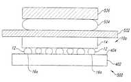
- FIG. 1is a side elevational view of a typical bumped device 10 (CSP, bumped die, etc.) mounted on, for example, a printed circuit board 20 .
- the bumped device 10includes a plurality of solder balls 12 attached to a plurality of ball pads (not shown) which are formed on a die 14 .
- Each solder ball 12has an outer edge 16 that aligns with a corresponding contact pad 18 on the printed circuit board 20 .
- a conductive lead 22is attached to each contact pad 18 .
- the outer edge 16 of each solder ball 12contacts the corresponding contact pad 18 during assembly of the bumped device 10 with the printed circuit board 20 , completing the electrical circuit between the conductive leads 22 and the die 14 .
- the height and width of the solder bumps 12 on the bumped device 10are not precisely uniform. Variation of the solder bump height and width depends on several factors, including variation in size of the original unattached solder balls, variation in the sizes of the ball pads, and differences in the attachment process.
- the nominal variation between the tallest and shortest ballsis presently about 60 microns ( ⁇ m). Therefore, when the device 10 is placed on a flat surface resting on the solder balls, the three tallest balls or bumps define the seating plane of the device, and the smaller balls do not touch the corresponding contact pads of the printed circuit board or test interposer.
- a moderate compression forcemay be applied to the bumped device 10 to drive the outer surfaces 16 of the solder balls 12 into contact with the contact pads 18 of the printed circuit board or test interposer 20 .
- the compression force needed to bring the solder bumps into contact with the contact padsvaries between 30 grams and 2000 grams depending upon the manufacturing or test process involved.
- the applied compression forceshould be kept to a minimum, however, because larger forces may damage the circuitry of the die 14 , the CSP solder balls, or the test interposer.
- micro-spring mounted contact pads 18are very expensive, relatively difficult to maintain, and may excessively damage the solder ball itself.
- an apparatus in accordance with the inventionincludes a planarization member engageable with at least some of the plurality of outer surfaces, and a securing element engageable with the bumped device to securely position the bumped device during engagement with the planarization member.
- the planarization memberapplies a planarization action on one or more of the outer surfaces to substantially planarize the plurality of outer surfaces.
- the planarization memberincludes a cutting tool and the planarization action comprises a milling action.
- the planarization memberincludes a heated platen and the planarization action comprises a thermo-mechanical deformation action.
- the planarization memberincludes an abrasive surface and the planarization action comprising a grinding action.
- the planarization memberincludes a chemical solution and the planarization action comprises a chemical reaction.
- the planarization memberincludes a solder deposition device and the planarization action comprises a solder deposition.
- an apparatusmay include a planarization gauge that measures a planarization condition of the outer surfaces.
- the planarization gaugemay measure the planarization condition before or after the planarization member is engaged with the outer surfaces.
- an apparatusin a further embodiment, includes a load device engageable with at least one of the bumped device or the planarization member to urge the at least some outer surfaces of the bumped device into engagement with the planarization member.
- the planarization memberapplies a planarization action on one or more of the plurality of outer surfaces to substantially planarize the plurality of outer surfaces.
- the planarization memberincludes a substantially flat surface and the load device includes a mass having a weight that urges the at least some outer surfaces into engagement with the flat surface to rat mechanically flatten the surfaces.
- the load deviceincludes a fixed surface and a pressurizable vessel, a pressure in the pressurizable vessel urging the bumped device away from the fixed surface and into engagement with the planarization member.
- the load deviceincludes a press engageable with the bumped device.
- the load deviceincludes a centrifuge engageable with the planarization member.
- FIG. 1is a side elevational view of a bumped device engaged with a printed circuit board in accordance with the prior art.
- FIG. 2is a side elevational view of the bumped device of FIG. 1 engaged with a planarization apparatus in accordance with an embodiment of the invention.
- FIG. 3is a side elevational view of the bumped device engaged with the printed circuit board of FIG. 1 following substantial planarization of the bumps in accordance with the invention.
- FIG. 4is a side elevational view of the bumped device of FIG. 1 engaged with a device having protruding contacts.
- FIG. 5is a side elevational view of the bumped device of FIG. 1 engaged with a planarization apparatus in accordance with an alternate embodiment of the invention.
- FIG. 6is a side elevational view of the bumped device of FIG. 1 engaged with an alternate embodiment of a planarization apparatus in accordance with the invention.
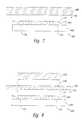
- FIG. 7is a side elevational view of an alternate embodiment of a planarization apparatus in accordance with the invention.
- FIG. 8is a side elevational view of another alternate embodiment of a planarization apparatus in accordance with the invention.
- FIG. 9is a side elevational view of yet another alternate embodiment of a planarization apparatus in accordance with the invention.
- FIG. 10shows a partial cross-sectional view of still another embodiment of a planarization apparatus in accordance with the invention.
- FIG. 2is a side elevational view of a bumped device 10 engaged with a planarization apparatus 100 in accordance with an embodiment of the invention.
- the planarization apparatus 100includes a rotating cutting head 102 with a plurality of cutting blades 104 .
- a securing element 106 having a recess 108 adapted to receive the bumped device 10is engaged with the bumped device 10 to secure the bumped device 10 in position during engagement of the solder balls 12 with the cutting head 102 .
- a planarization gauge (or sensor) 109is positioned proximate the bumped device 10 to measure (or sense) a planarization condition of the outer surfaces 16 of the solder balls 12 .
- bumped devicerefers not only to the bumped die depicted in FIG. 2, but also to a wide variety of microelectronics devices having solder bumps, including CSP's, flip-chips, ball grid array (BGA) packages, and micro-BGA packages.
- bumped deviceis intended herein to include multiples or combinations of bumped devices, such as an entire wafer of bumped dice prior to die singulation, or an entire handling tray containing multiple bumped packages.
- the securing element 106secures the bumped device 10 in position for engagement of the bumped device 10 with the cutting head 102 .
- the cutting blades 104rotate (as indicated by arrow w) and engage the outer surfaces 16 of the tallest solder bumps 12 .
- the cutting blades 104perform a planarization action (i.e. subtractive cutting or milling) on the outer surfaces 16 of one or more of the bumps 12 .
- the gauge 109may be used to check the outer surfaces 16 , 16 a to determine whether the solder balls 12 are all approximately the same height. If the outer surfaces are not planarized to the desired tolerance, the planarization apparatus 100 may be re-engaged with the outer surfaces 16 , 16 a one or more times until the balls are substantially planarized.
- planarizedand “planarization” are used throughout this discussion to refer to the fact that the solder balls 12 are made to be approximately the same height—that is to say, the solder balls project from the bumped device by approximately the same distance or thickness. It is not intended to imply that the outer surfaces 16 of all of the solder balls 12 are made flat. As shown in FIG. 2, the planarization apparatus 100 need not engage all of the solder balls 12 , and solder balls of different heights are engaged to different degrees. The actual number of solder balls engaged by the planarization apparatus 100 will depend upon the height variation of the balls of the array. Thus, some of the outer surfaces 16 a of the solder balls 12 may be flattened, and some will remain rounded. Following application of the planarization action, the plurality of solder balls on the bumped device will be substantially (i.e. approximately) the same height, a condition referred to as “substantially planarized.”
- a planarization member 100 Aincludes a cutting tool 103 that is oriented approximately perpendicular to the die 14 .
- the cutting tool 103may be positioned on a controllably driven base (not shown) and may be sized to apply a planarization action on a single solder bump 12 .
- the cutting tool 103allows individual solder balls 12 to be selected for milling.
- the cutting tool 103could also be used to remove most or all of a damaged ball. The ball could then be replaced by installation of a pre-formed ball, or by successive deposition of layers of solder using a solder deposition process, as described more fully below.
- planarization gauge 109is depicted in FIG. 2 as being an optical device that senses the planarity of the outer surfaces 16 , 16 a , such as the type of laser-based gauges disclosed in U.S. Pat. No. 5,663,797 to Sandhu for detecting the endpoint in chemical-mechanical polishing of semiconductor wafers.
- the gauge 109may be of any type that is suitable for detecting the heights of the solder bumps, including feeler gauges that physically contact the solder bumps or non-contacting capacitative-type height gauges.
- the planarization gauge 109may be incorporated into either the planarization member 100 , 100 A or the securing element 106 , or by proper control of the planarization member and securing element, the gauge may be eliminated.
- the gauge 109could measure all the balls 12 on the package 10 and then the planarization member 100 , 100 A could be directed to only mill off the “tallest” balls.
- the balls chosen to receive the planarization actioncould be determined by, for example, a software program.
- the software programcould accept input signals from the gauge 109 and transmit control signals to a controller which controllably positions the planarization member 100 , 100 A to act on the tallest solder balls 12 , thus substantially planarizing the solder balls in a fully-automated, controlled fashion.
- FIG. 3is a side elevational view of the bumped device 10 engaged with the printed circuit board 20 of FIG. 1 following substantial planarization of the outer surfaces 16 , 16 a . After engagement with the planarization apparatus 100 , most or all of the outer surfaces 16 , 16 a are in contact with the corresponding contact pads 18 on the printed circuit board 20 .
- An advantage of substantially planarizing the outer surfaces 16 , 16 a of the bumped device 10is that testing of the die 14 is significantly enhanced. Because the solder balls 12 are brought into contact with the contact pads 18 with minimal applied force, reliable testing of the die may be achieved without damaging the circuitry of the die.
- Another advantage of substantially planarizing the outer surfaces of the solder bumpsis that expensive micro-spring contact devices are eliminated. Significant cost and maintenance savings may be realized using the relatively simple, economical planarization member compared with the purchase or fabrication of a test interposer having micro-spring mounted contact devices.
- FIG. 4shows the bumped device 10 having substantially planarized solder bumps 12 engaged with a test interposer 20 a having protruding contacts 18 a .
- the height h of the protruding contacts 18 awould need to be on the order of 60 ⁇ m—the nominal variation between the tallest and shortest balls without planarization (shown as distance d on FIG. 1 ).
- the required height of the protruding contacts 18 a on the test interposer 20 ais reduced to about 20 ⁇ m, which is just enough to penetrate a layer of surface oxides on the solder balls for testing of the bumped device 10 .
- FIG. 5is a side elevational view of the bumped device 10 of FIG. 1 engaged with an alternate embodiment of a planarization apparatus 200 in accordance with the invention.
- the planarization apparatus 200includes a heated platen 202 having a substantially flat surface 204 engageable with the outer surfaces 16 of the solder balls 12 , and a securing element 206 having an aperture 208 therethrough.
- the bumped device 10is securely engaged within the aperture 208 so that the securing element 206 secures and positions the device during engagement with the heated platen 202 .
- the outer surfacesare heated by the flat surface 204 of the platen.
- the outer surfacesmay be softened and mechanically flattened by the flat surface 204 , or may be heated until the solder sublimates. In either case, these thermo-mechanical actions performed by the heated platen 202 on the solder balls 12 substantially planarize the outer surfaces 16 a to an approximately uniform height.
- the platen 202is preferably made of a material that the solder will not wet to. Also, if the platen 202 is removed from the ball while the ball is still in a liquid state, then the surface tension of the ball may cause the ball to reform into its original undesirable spherical shape. Thus, if the platen 202 temperature is sufficient to liquify the solder ball 12 , then after the ball has been liquified and mechanically reformed, it is preferable that the platen 202 temperature be reduced while the platen remains in contact with the ball 12 until the solder ball solidifies into a substantially planarized shape.
- the heated platen 202is shown in FIG. 5 as only contacting four of the solder balls 12 , it is apparent that the platen may be made as large or as small as desirable.
- the platenmay, for example, be coextensive with all the balls of the bumped device 10 .
- the heated platenmay be configured to contact only one ball (or one row) at a time, such as by using a roller, a blade, a squeegee, or other configuration.
- the planarization apparatus 200includes a grinding member 202 having an abrasive surface 204 engageable with the outer surfaces 16 of the solder bumps 12 .
- the grinding member 202is laterally moveable (indicated in FIG. 4 by the double-headed arrow h) with respect to the solder bumps 12 .
- the abrasive surface 204performs a grinding action on one or more of the bumps 12 , thereby substantially planarizing the outer surfaces 16 a.
- the grinding membermay rotate with respect to the bumps in a manner similar to the chemical-mechanical polishing (CMP) devices for planarization of silicon wafers, including, for example, the types disclosed in U.S. Pat. No. 5,738,567 to Manzonie and Akram.
- CMPchemical-mechanical polishing
- the abrasive surface 204may be used with a polishing solution that helps to dissolve the outer surfaces of the solder bumps, or an abrasive slurry that assists in the physical removal of material from the outer surfaces.
- planarization apparatus in accordance with the inventionused to planarize the solder balls of flip-chip chip devices while still in whole wafer form, prior to die singulation of the wafer.
- the planarization apparatus 200includes a reactive member 202 having a chemically-coated or wetted surface 204 .
- a chemical actionis performed on the solder bumps which dissolves the outer edges of the tallest bumps, making the bumps approximately the same height and substantially planarizing the outer surfaces 16 , 16 a .
- Suitable chemicals for coating or wetting the surface 204 for chemically reacting with the solder ballsare known in the industry, as discussed in greater detail below.
- Many alternate embodiments of securing elementsare available, including, for example, those having recesses (FIG. 1 ), apertures (FIG. 2 ), pinching mechanisms, clamping mechanisms, or suction mechanisms. In general, all types of securing elements that securely position the bumped device during engagement with the planarization member are acceptable.
- FIG. 6is a side elevational view of the bumped device 10 of FIG. 1 engaged with an alternate embodiment of a planarization apparatus 300 in accordance with the invention.
- the planarization apparatus 300has a pair of contact posts 302 that contact the outer surfaces 16 of the solder balls 12 , and a solder deposition device 304 .
- the solder deposition device 304deposits a solder buildup layer 308 on selected solder balls 12 .
- a securing element 306pinches the substrate 14 of the bumped device 10 to securely position the device during engagement with the solder deposition device 304 .
- the contact posts 302systematically contact the outer surfaces 16 of at least some of the solder balls 12 to determine the highest solder balls 12 .
- the highest solder ballsthen define a seating plane 307 .
- the seating plane 307may be defined by the three tallest balls or, if desired, from the single tallest ball.
- the seating plane 307may be determined from the two tallest balls or the single tallest ball.
- the process involving definition of the seating plane 307may be employed equally well with the planarization apparatus that employ “substractive” planarization actions, such as the rotating cutter or the heated platen.
- damaged ballsmay be partially or wholly removed and replaced until the solder balls 12 are substantially planarized.
- inventive apparatus and processesmay be used to rework or repair bumped devices 10 with missing or damaged solder balls.
- planarization apparatus 300is shown in FIG. 6 as having two contact posts 302 , it should be recognized that many alternative ways of defining the seating plane 307 exist.
- the planarization apparatus 300may have only a single contact post that is used to sample the heights the solder bumps, or may have a contact post for each of the solder bumps on the bumped device 10 .
- the planarization apparatus 300may have a single, adjustably positionable solder deposition device 304 as shown in FIG. 6, or many solder deposition devices, such as one solder deposition device per solder bump.
- the solder deposition device 304may include a solder jet, or a solder ball bumper, or other suitable device. Representative, commercially-available devices include the drop-on demand solder jet systems from MPM Corporation of Franklin, Mass., or the solder ball bumper Model SB 2 M from Packaging Technologies, GmbH of Germany.
- the seating plane 307may be defined at any desired intermediate level that is somewhere between the highest and lowest bumps.
- the solder deposition device 304could be used to build up the heights of the shorter solder bumps 12
- another planarization membere.g. cutting head, heated platen, etc.
- FIG. 7is a side elevational view of an alternate embodiment of a planarization apparatus 400 in accordance with the invention.
- This embodiment of the planarization apparatus 400is suitable for use with, for example, a bumped device 10 a that is capable of withstanding a moderate or larger compression load without sustaining damage.
- the planarization apparatus 400includes a planarization chuck 402 having a substantially flat surface 404 , and a retaining mass 406 engaged with the substrate 14 of the bumped device 10 a.
- the bumped device 10 ais positioned with the solder balls 12 facing the flat surface 404 of the planarization chuck 402 , and the retaining mass 406 is engaged onto the bumped device 10 a .
- the retaining mass 406secures the bumped device 10 a into engagement with the planarization chuck 402 , and the weight of the retaining mass 406 compresses the solder balls 12 against the flat surface 404 , flattening the outer surfaces 16 of some or all of the balls, particularly the tallest balls.
- the compression caused by the weight of the retaining massmechanically deforms the outer surfaces 16 a , thereby substantially planarizing the outer surfaces 16 , 16 a of the solder balls.
- the planarization member 400advantageously provides the benefits of substantial planarization of the solder balls using a simple, inexpensive, and easily maintainable system.
- FIG. 8shows an alternate embodiment of a planarization apparatus 500 having a pressure plate 532 engaged against the bumped die 10 a opposite from the planarization chuck 402 .
- a pressurizable vessel 534is positioned above the pressure plate 532 , and a fixed wall 536 is positioned over the pressurizable vessel 534 .
- the pressure in the vesselforces the pressure plate 532 downward against the bumped die 10 a , compressing e solder balls 12 against the flat surface 404 and flattening the outer surfaces 6 a.
- the pressure plate 532is removed, and the pressurizable vessel 534 engages the bumped die 10 a directly to apply the compression force.
- the compression forcecould be generated by any number of devices which are commonly known in the industry, including, for example, a press, a motor and mechanical linkage, or other devices.
- FIG. 9is a side elevational view of yet another embodiment of a planarization apparatus 600 in accordance with the invention.
- the planarization apparatus 600includes a planarization chuck 602 having a substantially flat surface 604 , and a centrifuge 610 .
- a pair of securing members (or clips) 606engage and secure the bumped device 10 a in position on the planarization chuck 602 with the solder balls 12 of the bumped device 10 a engaged with the flat surface 604 .
- the centrifuge 610is rotated as depicted by arrow R.
- the rotation of the centrifugegenerates a centrifugal force that compresses the bumped device 10 a against the planarization chuck 602 .
- the securing members 606secure the bumped device 10 a in position on the planarization chuck 602 .
- a centrifugal forcebegins to press some or all of the solder bumps 12 into the flat surface 604 , substantially flattening the outer surfaces 16 a against the flat surface 604 . As shown in FIG.
- one or more planarization chucks 602may be disposed within the centrifuge 610 for simultaneously planarizing more than one bumped device 10 a .
- the centrifuge 610advantageously eliminates the use of weights, pressurization vessels, or other devices used to generate the compression force.
- FIG. 10shows a partial cross-sectional view of still another embodiment of a planarization apparatus 700 in accordance with the invention.
- the planarization apparatus 700includes a receptacle 702 having a retaining wall 704 .
- the retaining wall 704partially encloses a receiving space 706 that is sized to receivably engage the bumped device 10 . With the bumped device 10 placed in an inverted position within the receiving space 706 , the retaining wall 704 projects above the outer surfaces 16 b of the tallest solder bumps 12 (shown in dashed lines).
- a protective layer 740is disposed on the bumped device 10 within the receiving space 706 , the protective layer 740 at least partially surrounding and encasing the solder bumps 12 .
- the protective layer 740includes an upper surface 707 .
- a reactive solution 750is disposed within the receiving space 706 on the upper surface 707 of the protective layer 740 , and a planarization gauge 109 is positioned proximate the receptacle 702 .
- the protective layer 740is formed so that its thickness is approximately equal to the height of the shortest solder bump 12 .
- the upper surface 707thereby defines a seating plane through which the outer surfaces 16 b project.
- the reactive solution 750is then deposited into the receiving space 706 to chemically react with and dissolve (i.e. etch) the outer surfaces 16 b of the solder bumps 12 .
- the protective layer 740is comprised of one or more materials that are resistive or inert to the reactive solution 750 . As the reactive solution 750 etches the projecting portion of the outer surfaces 16 b , the planarization gauge 109 monitors a planarization condition of the seating plane and outer surfaces (as discussed above).
- the reactive solution 750is removed.
- the protective layer 740is then etched or dissolved using a suitable solution or other process (e.g. by heating) that removes the protective layer but does not harm the solder bumps 12 .
- the heights of the solder bumps 12 on the bumped device 10are thereby substantially planarized.
- Suitable reactive solutions 750 for etching the solder balls 12are known, and include, for example, ammonium bifluoride/peroxide, nitric/ferric nitrate acid, nitric/hydrofluoric acid, or a two-step combination of nitric acid followed by ferric chloride.
- suitable materials for the protective layer 740are widely known.
- planarization gauge 109could be incorporated into the receptacle 702 , such as by being disposed within the retaining wall 704 . Alternately, by proper control or calibration of the reactive solution 750 and/or the solder composition, the planarization gauge 109 may be eliminated.
- the bumped device 10is re-positioned with the solder bumps 12 projecting downwardly, and the reactive solution 750 is contained in a vat or reservoir below the bumped device 10 .
- the bumped device 10could be controllably lowered (or the reservoir of reactive solution raised) until some or all of the outer surfaces 16 , but at least the outer surfaces 16 b of the tallest solder bumps, come into contact with the reactive solution 750 .
- the reactive solution 750then etches and dissolves the outer surfaces that come into contact with the reactive solution, dissolving the outer surfaces and substantially planarizing the solder bumps.
- the protective layer 740 , the retaining wall 704 , and the planarization gauge 109may be eliminated.
- the benefits of substantial planarization of the solder balls 12are achieved using a relatively simple, easily maintainable planarization system.
- planarization apparatusprovides improved testing, manufacture, and packaging of bumped devices by substantially planarizing the outer surfaces of the solder balls.
- substantial planarization of the solder bumpsthe compression forces needed to engage the solder balls 12 into contact with the contact pads 18 or a test interposer, printed circuit board, or other bumped device are substantially reduced or eliminated, thereby improving reliability and avoiding damage to the bumped device.
- Expensive alternativessuch as micro-spring contact pads, are eliminated.
- Another advantageis that substantial planarization of the solder balls improves the engagement of the bumped device with a device having pedestal or protruding contacts, simplifying the manufacturing and reducing the cost of such devices.
Landscapes
- Engineering & Computer Science (AREA)
- Manufacturing & Machinery (AREA)
- Mechanical Engineering (AREA)
- Microelectronics & Electronic Packaging (AREA)
- Ceramic Engineering (AREA)
- Power Engineering (AREA)
- Computer Hardware Design (AREA)
- Inorganic Chemistry (AREA)
- General Physics & Mathematics (AREA)
- Condensed Matter Physics & Semiconductors (AREA)
- Physics & Mathematics (AREA)
- Chemical & Material Sciences (AREA)
- Electric Connection Of Electric Components To Printed Circuits (AREA)
- Wire Bonding (AREA)
Abstract
Description
Claims (18)
Priority Applications (1)
| Application Number | Priority Date | Filing Date | Title |
|---|---|---|---|
| US09/900,330US6431952B2 (en) | 1999-08-09 | 2001-07-05 | Apparatus and methods for substantial planarization of solder bumps |
Applications Claiming Priority (2)
| Application Number | Priority Date | Filing Date | Title |
|---|---|---|---|
| US09/370,498US6267650B1 (en) | 1999-08-09 | 1999-08-09 | Apparatus and methods for substantial planarization of solder bumps |
| US09/900,330US6431952B2 (en) | 1999-08-09 | 2001-07-05 | Apparatus and methods for substantial planarization of solder bumps |
Related Parent Applications (1)
| Application Number | Title | Priority Date | Filing Date |
|---|---|---|---|
| US09/370,498DivisionUS6267650B1 (en) | 1999-08-09 | 1999-08-09 | Apparatus and methods for substantial planarization of solder bumps |
Publications (2)
| Publication Number | Publication Date |
|---|---|
| US20010039165A1 US20010039165A1 (en) | 2001-11-08 |
| US6431952B2true US6431952B2 (en) | 2002-08-13 |
Family
ID=23459930
Family Applications (14)
| Application Number | Title | Priority Date | Filing Date |
|---|---|---|---|
| US09/370,498Expired - LifetimeUS6267650B1 (en) | 1999-08-09 | 1999-08-09 | Apparatus and methods for substantial planarization of solder bumps |
| US09/715,691Expired - LifetimeUS6416395B1 (en) | 1999-08-09 | 2000-11-17 | Apparatus and methods for substantial planarization of solder bumps |
| US09/900,301Expired - LifetimeUS6416386B2 (en) | 1999-08-09 | 2001-07-05 | Apparatus and methods for substantial planarization of solder bumps |
| US09/899,897Expired - LifetimeUS6416397B2 (en) | 1999-08-09 | 2001-07-05 | Apparatus and methods for substantial planarization of solder bumps |
| US09/900,330Expired - LifetimeUS6431952B2 (en) | 1999-08-09 | 2001-07-05 | Apparatus and methods for substantial planarization of solder bumps |
| US09/907,835Expired - LifetimeUS6416398B2 (en) | 1999-08-09 | 2001-07-17 | Apparatus and methods for substantial planarization of solder bumps |
| US09/907,789Expired - Fee RelatedUS6416387B2 (en) | 1999-08-09 | 2001-07-17 | Apparatus and methods for substantial planarization of solder bumps |
| US09/908,882Expired - Fee RelatedUS6416388B2 (en) | 1999-08-09 | 2001-07-18 | Apparatus and methods for substantial planarization of solder bumps |
| US09/910,407Expired - Fee RelatedUS6416399B2 (en) | 1999-08-09 | 2001-07-19 | Apparatus and methods for substantial planarization of solder bumps |
| US09/910,312Expired - LifetimeUS6422923B2 (en) | 1999-08-09 | 2001-07-19 | Apparatus and methods for substantial planarization of solder bumps |
| US09/910,334Expired - Fee RelatedUS6422919B2 (en) | 1999-08-09 | 2001-07-19 | Apparatus and methods for substantial planarization of solder bumps |
| US09/910,320Expired - LifetimeUS6419550B2 (en) | 1999-08-09 | 2001-07-19 | Apparatus and methods for substantial planarization of solder bumps |
| US09/919,268Expired - Fee RelatedUS6543267B2 (en) | 1999-08-09 | 2001-07-30 | Apparatus and methods for substantial planarization of solder bumps |
| US09/919,267Expired - LifetimeUS6503127B2 (en) | 1999-08-09 | 2001-07-30 | Apparatus and methods for substantial planarization of solder bumps |
Family Applications Before (4)
| Application Number | Title | Priority Date | Filing Date |
|---|---|---|---|
| US09/370,498Expired - LifetimeUS6267650B1 (en) | 1999-08-09 | 1999-08-09 | Apparatus and methods for substantial planarization of solder bumps |
| US09/715,691Expired - LifetimeUS6416395B1 (en) | 1999-08-09 | 2000-11-17 | Apparatus and methods for substantial planarization of solder bumps |
| US09/900,301Expired - LifetimeUS6416386B2 (en) | 1999-08-09 | 2001-07-05 | Apparatus and methods for substantial planarization of solder bumps |
| US09/899,897Expired - LifetimeUS6416397B2 (en) | 1999-08-09 | 2001-07-05 | Apparatus and methods for substantial planarization of solder bumps |
Family Applications After (9)
| Application Number | Title | Priority Date | Filing Date |
|---|---|---|---|
| US09/907,835Expired - LifetimeUS6416398B2 (en) | 1999-08-09 | 2001-07-17 | Apparatus and methods for substantial planarization of solder bumps |
| US09/907,789Expired - Fee RelatedUS6416387B2 (en) | 1999-08-09 | 2001-07-17 | Apparatus and methods for substantial planarization of solder bumps |
| US09/908,882Expired - Fee RelatedUS6416388B2 (en) | 1999-08-09 | 2001-07-18 | Apparatus and methods for substantial planarization of solder bumps |
| US09/910,407Expired - Fee RelatedUS6416399B2 (en) | 1999-08-09 | 2001-07-19 | Apparatus and methods for substantial planarization of solder bumps |
| US09/910,312Expired - LifetimeUS6422923B2 (en) | 1999-08-09 | 2001-07-19 | Apparatus and methods for substantial planarization of solder bumps |
| US09/910,334Expired - Fee RelatedUS6422919B2 (en) | 1999-08-09 | 2001-07-19 | Apparatus and methods for substantial planarization of solder bumps |
| US09/910,320Expired - LifetimeUS6419550B2 (en) | 1999-08-09 | 2001-07-19 | Apparatus and methods for substantial planarization of solder bumps |
| US09/919,268Expired - Fee RelatedUS6543267B2 (en) | 1999-08-09 | 2001-07-30 | Apparatus and methods for substantial planarization of solder bumps |
| US09/919,267Expired - LifetimeUS6503127B2 (en) | 1999-08-09 | 2001-07-30 | Apparatus and methods for substantial planarization of solder bumps |
Country Status (1)
| Country | Link |
|---|---|
| US (14) | US6267650B1 (en) |
Cited By (5)
| Publication number | Priority date | Publication date | Assignee | Title |
|---|---|---|---|---|
| US6508845B1 (en)* | 2000-06-28 | 2003-01-21 | Advanced Micro Devices, Inc. | Method and apparatus for precoining BGA type packages prior to electrical characterization |
| US6543267B2 (en)* | 1999-08-09 | 2003-04-08 | Micron Technology, Inc. | Apparatus and methods for substantial planarization of solder bumps |
| US20040188261A1 (en)* | 2003-03-27 | 2004-09-30 | Scimed Life Systems, Inc. | Methods of forming medical devices |
| US20050161814A1 (en)* | 2002-12-27 | 2005-07-28 | Fujitsu Limited | Method for forming bumps, semiconductor device and method for manufacturing same, substrate processing apparatus, and semiconductor manufacturing apparatus |
| US20090111299A1 (en)* | 2007-10-31 | 2009-04-30 | International Business Machines Corporation | Surface Mount Array Connector Leads Planarization Using Solder Reflow Method |
Families Citing this family (82)
| Publication number | Priority date | Publication date | Assignee | Title |
|---|---|---|---|---|
| JPH1013007A (en)* | 1996-03-29 | 1998-01-16 | Ngk Spark Plug Co Ltd | Wiring board with solder bump, its manufacturing method, and flattening tool |
| US6368647B1 (en)* | 1998-12-29 | 2002-04-09 | Mars, Incorporated | Ultrasonically activated continuous slitter apparatus and method |
| US6419500B1 (en)* | 1999-03-08 | 2002-07-16 | Kulicke & Soffa Investment, Inc. | Probe assembly having floatable buckling beam probes and apparatus for abrading the same |
| US6383934B1 (en) | 1999-09-02 | 2002-05-07 | Micron Technology, Inc. | Method and apparatus for chemical-mechanical planarization of microelectronic substrates with selected planarizing liquids |
| US6306768B1 (en) | 1999-11-17 | 2001-10-23 | Micron Technology, Inc. | Method for planarizing microelectronic substrates having apertures |
| US6313038B1 (en) | 2000-04-26 | 2001-11-06 | Micron Technology, Inc. | Method and apparatus for controlling chemical interactions during planarization of microelectronic substrates |
| US6387289B1 (en)* | 2000-05-04 | 2002-05-14 | Micron Technology, Inc. | Planarizing machines and methods for mechanical and/or chemical-mechanical planarization of microelectronic-device substrate assemblies |
| US6612901B1 (en) | 2000-06-07 | 2003-09-02 | Micron Technology, Inc. | Apparatus for in-situ optical endpointing of web-format planarizing machines in mechanical or chemical-mechanical planarization of microelectronic-device substrate assemblies |
| US6465338B1 (en)* | 2000-07-10 | 2002-10-15 | Lsi Logic Corporation | Method of planarizing die solder balls by employing a die's weight |
| US6838382B1 (en)* | 2000-08-28 | 2005-01-04 | Micron Technology, Inc. | Method and apparatus for forming a planarizing pad having a film and texture elements for planarization of microelectronic substrates |
| US6736869B1 (en) | 2000-08-28 | 2004-05-18 | Micron Technology, Inc. | Method for forming a planarizing pad for planarization of microelectronic substrates |
| JP3829050B2 (en)* | 2000-08-29 | 2006-10-04 | 松下電器産業株式会社 | Integrated electronic components |
| US6652764B1 (en) | 2000-08-31 | 2003-11-25 | Micron Technology, Inc. | Methods and apparatuses for making and using planarizing pads for mechanical and chemical-mechanical planarization of microelectronic substrates |
| SG97164A1 (en) | 2000-09-21 | 2003-07-18 | Micron Technology Inc | Individual selective rework of defective bga solder balls |
| US6719188B2 (en)* | 2001-07-24 | 2004-04-13 | International Business Machines Corporation | Rework methods for lead BGA/CGA |
| JP3981817B2 (en)* | 2001-08-08 | 2007-09-26 | セイコーエプソン株式会社 | Manufacturing method of semiconductor device |
| US6722943B2 (en) | 2001-08-24 | 2004-04-20 | Micron Technology, Inc. | Planarizing machines and methods for dispensing planarizing solutions in the processing of microelectronic workpieces |
| US7656678B2 (en) | 2001-10-26 | 2010-02-02 | Entorian Technologies, Lp | Stacked module systems |
| US7371609B2 (en)* | 2001-10-26 | 2008-05-13 | Staktek Group L.P. | Stacked module systems and methods |
| US6635572B1 (en)* | 2001-11-28 | 2003-10-21 | Advanced Micro Devices, Inc. | Method of substrate silicon removal for integrated circuit devices |
| US6504108B1 (en)* | 2001-12-28 | 2003-01-07 | Hon Hai Precision Ind. Co., Ltd. | Electrical connector having stand-offs between solder balls thereof |
| US7131889B1 (en)* | 2002-03-04 | 2006-11-07 | Micron Technology, Inc. | Method for planarizing microelectronic workpieces |
| US6869335B2 (en) | 2002-07-08 | 2005-03-22 | Micron Technology, Inc. | Retaining rings, planarizing apparatuses including retaining rings, and methods for planarizing micro-device workpieces |
| US7341502B2 (en) | 2002-07-18 | 2008-03-11 | Micron Technology, Inc. | Methods and systems for planarizing workpieces, e.g., microelectronic workpieces |
| US6860798B2 (en)* | 2002-08-08 | 2005-03-01 | Micron Technology, Inc. | Carrier assemblies, planarizing apparatuses including carrier assemblies, and methods for planarizing micro-device workpieces |
| US7094695B2 (en)* | 2002-08-21 | 2006-08-22 | Micron Technology, Inc. | Apparatus and method for conditioning a polishing pad used for mechanical and/or chemical-mechanical planarization |
| US7004817B2 (en) | 2002-08-23 | 2006-02-28 | Micron Technology, Inc. | Carrier assemblies, planarizing apparatuses including carrier assemblies, and methods for planarizing micro-device workpieces |
| US7011566B2 (en)* | 2002-08-26 | 2006-03-14 | Micron Technology, Inc. | Methods and systems for conditioning planarizing pads used in planarizing substrates |
| US7008299B2 (en)* | 2002-08-29 | 2006-03-07 | Micron Technology, Inc. | Apparatus and method for mechanical and/or chemical-mechanical planarization of micro-device workpieces |
| US6841991B2 (en)* | 2002-08-29 | 2005-01-11 | Micron Technology, Inc. | Planarity diagnostic system, E.G., for microelectronic component test systems |
| US20040099962A1 (en)* | 2002-11-22 | 2004-05-27 | Sarathy Rajagopalan | Flip chip electrical test yields by countering substrate die area coplanarity |
| GB0228929D0 (en) | 2002-12-11 | 2003-01-15 | R W Data Ltd | Structured cabling system and method |
| CN101483144B (en)* | 2002-12-27 | 2013-08-28 | 富士通株式会社 | Method for forming bumps, semiconductor device and method for manufacturing same, substrate processing apparatus, and semiconductor manufacturing apparatus |
| US7074114B2 (en) | 2003-01-16 | 2006-07-11 | Micron Technology, Inc. | Carrier assemblies, polishing machines including carrier assemblies, and methods for polishing micro-device workpieces |
| US6884152B2 (en) | 2003-02-11 | 2005-04-26 | Micron Technology, Inc. | Apparatuses and methods for conditioning polishing pads used in polishing micro-device workpieces |
| US6872132B2 (en) | 2003-03-03 | 2005-03-29 | Micron Technology, Inc. | Systems and methods for monitoring characteristics of a polishing pad used in polishing micro-device workpieces |
| JP2004319697A (en)* | 2003-04-15 | 2004-11-11 | Disco Abrasive Syst Ltd | Equipment for processing electrodes formed on plate-like objects |
| JP4057457B2 (en)* | 2003-04-15 | 2008-03-05 | 株式会社ディスコ | Flip chip bonder |
| US6935929B2 (en) | 2003-04-28 | 2005-08-30 | Micron Technology, Inc. | Polishing machines including under-pads and methods for mechanical and/or chemical-mechanical polishing of microfeature workpieces |
| US7131891B2 (en)* | 2003-04-28 | 2006-11-07 | Micron Technology, Inc. | Systems and methods for mechanical and/or chemical-mechanical polishing of microfeature workpieces |
| US7030603B2 (en) | 2003-08-21 | 2006-04-18 | Micron Technology, Inc. | Apparatuses and methods for monitoring rotation of a conductive microfeature workpiece |
| US7040965B2 (en)* | 2003-09-18 | 2006-05-09 | Micron Technology, Inc. | Methods for removing doped silicon material from microfeature workpieces |
| US6939211B2 (en)* | 2003-10-09 | 2005-09-06 | Micron Technology, Inc. | Planarizing solutions including abrasive elements, and methods for manufacturing and using such planarizing solutions |
| US7134029B2 (en)* | 2003-11-06 | 2006-11-07 | International Business Machines Corporation | Computer-component power-consumption monitoring and control |
| US7086927B2 (en) | 2004-03-09 | 2006-08-08 | Micron Technology, Inc. | Methods and systems for planarizing workpieces, e.g., microelectronic workpieces |
| US20050242161A1 (en)* | 2004-04-30 | 2005-11-03 | Visteon Global Technologies, Inc. | Systems and methods for laser soldering flat flexible cable |
| US7066792B2 (en)* | 2004-08-06 | 2006-06-27 | Micron Technology, Inc. | Shaped polishing pads for beveling microfeature workpiece edges, and associate system and methods |
| US7033253B2 (en)* | 2004-08-12 | 2006-04-25 | Micron Technology, Inc. | Polishing pad conditioners having abrasives and brush elements, and associated systems and methods |
| US7153191B2 (en)* | 2004-08-20 | 2006-12-26 | Micron Technology, Inc. | Polishing liquids for activating and/or conditioning fixed abrasive polishing pads, and associated systems and methods |
| US7396752B1 (en)* | 2004-11-10 | 2008-07-08 | Altera Corporation | Method and apparatus for reducing cold joint defects in flip chip products |
| JP4709535B2 (en)* | 2004-11-19 | 2011-06-22 | 株式会社東芝 | Semiconductor device manufacturing equipment |
| US20060163330A1 (en)* | 2005-01-26 | 2006-07-27 | International Business Machines Corporation | Site flattening tool and method for circuit board repair |
| US7264539B2 (en) | 2005-07-13 | 2007-09-04 | Micron Technology, Inc. | Systems and methods for removing microfeature workpiece surface defects |
| US7438626B2 (en) | 2005-08-31 | 2008-10-21 | Micron Technology, Inc. | Apparatus and method for removing material from microfeature workpieces |
| US7326105B2 (en) | 2005-08-31 | 2008-02-05 | Micron Technology, Inc. | Retaining rings, and associated planarizing apparatuses, and related methods for planarizing micro-device workpieces |
| US7294049B2 (en) | 2005-09-01 | 2007-11-13 | Micron Technology, Inc. | Method and apparatus for removing material from microfeature workpieces |
| KR100712534B1 (en)* | 2005-09-22 | 2007-04-27 | 삼성전자주식회사 | Package and test device having a ball to minimize contact resistance, and method of manufacturing the package |
| TWI378517B (en)* | 2006-02-27 | 2012-12-01 | Chipmos Technologies Inc | Bumping process |
| US20080197493A1 (en)* | 2007-02-16 | 2008-08-21 | Stefan Geyer | Integrated circuit including conductive bumps |
| US7754612B2 (en) | 2007-03-14 | 2010-07-13 | Micron Technology, Inc. | Methods and apparatuses for removing polysilicon from semiconductor workpieces |
| JP5215773B2 (en)* | 2008-08-18 | 2013-06-19 | 株式会社ディスコ | Processing method |
| US9006028B2 (en)* | 2008-09-12 | 2015-04-14 | Ananda H. Kumar | Methods for forming ceramic substrates with via studs |
| KR101019642B1 (en)* | 2009-04-27 | 2011-03-07 | 삼성전기주식회사 | Printed Circuit Board Manufacturing Method |
| KR101131445B1 (en) | 2010-05-24 | 2012-03-29 | 앰코 테크놀로지 코리아 주식회사 | Apparatus for removing of solder ball on semiconductor package |
| WO2013129980A1 (en) | 2012-02-27 | 2013-09-06 | Telefonaktiebolaget L M Ericsson (Publ) | Method and apparatus for forming solder bumps |
| US9159687B2 (en) | 2012-07-31 | 2015-10-13 | Taiwan Semiconductor Manufacturing Company, Ltd. | Solder bump for ball grid array |
| US9207275B2 (en)* | 2012-12-14 | 2015-12-08 | International Business Machines Corporation | Interconnect solder bumps for die testing |
| JP6197319B2 (en)* | 2013-03-21 | 2017-09-20 | 富士通株式会社 | Mounting method of semiconductor element |
| US9881889B2 (en)* | 2013-04-12 | 2018-01-30 | Xintec Inc. | Chip package and method for fabricating the same |
| KR20150004005A (en)* | 2013-07-02 | 2015-01-12 | 에스케이하이닉스 주식회사 | Stacked semiconductor package and manufacturing method of the same |
| JP6064831B2 (en)* | 2013-08-08 | 2017-01-25 | 三菱電機株式会社 | Test equipment, test method |
| US10319619B2 (en)* | 2014-12-05 | 2019-06-11 | Samsung Electronics Co., Ltd. | Equipment for manufacturing semiconductor devices and method for use of same for manufacturing semiconductor package components |
| US20170023617A1 (en)* | 2015-06-10 | 2017-01-26 | Translarity, Inc. | Shaping of contact structures for semiconductor test, and associated systems and methods |
| WO2017142741A1 (en)* | 2016-02-19 | 2017-08-24 | Alpha Assembly Solutions Inc. | Rf shield with selectively integrated solder |
| US10001508B2 (en)* | 2016-06-17 | 2018-06-19 | International Business Machines Corporation | Integrated self-coining probe |
| CN111331443A (en)* | 2020-01-16 | 2020-06-26 | 南阳鼎泰高科有限公司 | Processing method for coarse grinding of PCB drill point blade |
| US11171101B2 (en) | 2020-03-31 | 2021-11-09 | Raytheon Company | Process for removing bond film from cavities in printed circuit boards |
| US11122692B1 (en)* | 2020-06-11 | 2021-09-14 | Raytheon Company | Preparation of solder bump for compatibility with printed electronics and enhanced via reliability |
| CN112008507A (en)* | 2020-09-08 | 2020-12-01 | 协易科技精机(中国)有限公司 | Matching grinding method suitable for ball-head type connecting rod |
| JP7699654B2 (en)* | 2020-11-23 | 2025-06-27 | オルボテック リミテッド | Solder Bump Repair |
| CN113059483A (en)* | 2021-03-19 | 2021-07-02 | 上海泽丰半导体科技有限公司 | Substrate leveling jig, leveling method and probe card |
| CN114928958A (en)* | 2022-06-24 | 2022-08-19 | 重庆中电天时精密装备技术有限公司 | PCB and PCBA plane precision press-fitting method |
Citations (12)
| Publication number | Priority date | Publication date | Assignee | Title |
|---|---|---|---|---|
| US5216843A (en) | 1992-09-24 | 1993-06-08 | Intel Corporation | Polishing pad conditioning apparatus for wafer planarization process |
| US5435482A (en)* | 1994-02-04 | 1995-07-25 | Lsi Logic Corporation | Integrated circuit having a coplanar solder ball contact array |
| US5575706A (en) | 1996-01-11 | 1996-11-19 | Taiwan Semiconductor Manufacturing Company Ltd. | Chemical/mechanical planarization (CMP) apparatus and polish method |
| US5643048A (en) | 1996-02-13 | 1997-07-01 | Micron Technology, Inc. | Endpoint regulator and method for regulating a change in wafer thickness in chemical-mechanical planarization of semiconductor wafers |
| US5658190A (en) | 1995-12-15 | 1997-08-19 | Micron Technology, Inc. | Apparatus for separating wafers from polishing pads used in chemical-mechanical planarization of semiconductor wafers |
| US5663797A (en)* | 1996-05-16 | 1997-09-02 | Micron Technology, Inc. | Method and apparatus for detecting the endpoint in chemical-mechanical polishing of semiconductor wafers |
| US5716264A (en) | 1995-07-18 | 1998-02-10 | Ebara Corporation | Polishing apparatus |
| US5738567A (en) | 1996-08-20 | 1998-04-14 | Micron Technology, Inc. | Polishing pad for chemical-mechanical planarization of a semiconductor wafer |
| US5738562A (en) | 1996-01-24 | 1998-04-14 | Micron Technology, Inc. | Apparatus and method for planar end-point detection during chemical-mechanical polishing |
| US5796590A (en)* | 1996-11-05 | 1998-08-18 | Micron Electronics, Inc. | Assembly aid for mounting packaged integrated circuit devices to printed circuit boards |
| US5879222A (en) | 1996-01-22 | 1999-03-09 | Micron Technology, Inc. | Abrasive polishing pad with covalently bonded abrasive particles |
| US6267650B1 (en)* | 1999-08-09 | 2001-07-31 | Micron Technology, Inc. | Apparatus and methods for substantial planarization of solder bumps |
- 1999
- 1999-08-09USUS09/370,498patent/US6267650B1/ennot_activeExpired - Lifetime
- 2000
- 2000-11-17USUS09/715,691patent/US6416395B1/ennot_activeExpired - Lifetime
- 2001
- 2001-07-05USUS09/900,301patent/US6416386B2/ennot_activeExpired - Lifetime
- 2001-07-05USUS09/899,897patent/US6416397B2/ennot_activeExpired - Lifetime
- 2001-07-05USUS09/900,330patent/US6431952B2/ennot_activeExpired - Lifetime
- 2001-07-17USUS09/907,835patent/US6416398B2/ennot_activeExpired - Lifetime
- 2001-07-17USUS09/907,789patent/US6416387B2/ennot_activeExpired - Fee Related
- 2001-07-18USUS09/908,882patent/US6416388B2/ennot_activeExpired - Fee Related
- 2001-07-19USUS09/910,407patent/US6416399B2/ennot_activeExpired - Fee Related
- 2001-07-19USUS09/910,312patent/US6422923B2/ennot_activeExpired - Lifetime
- 2001-07-19USUS09/910,334patent/US6422919B2/ennot_activeExpired - Fee Related
- 2001-07-19USUS09/910,320patent/US6419550B2/ennot_activeExpired - Lifetime
- 2001-07-30USUS09/919,268patent/US6543267B2/ennot_activeExpired - Fee Related
- 2001-07-30USUS09/919,267patent/US6503127B2/ennot_activeExpired - Lifetime
Patent Citations (15)
| Publication number | Priority date | Publication date | Assignee | Title |
|---|---|---|---|---|
| US5216843A (en) | 1992-09-24 | 1993-06-08 | Intel Corporation | Polishing pad conditioning apparatus for wafer planarization process |
| US5435482A (en)* | 1994-02-04 | 1995-07-25 | Lsi Logic Corporation | Integrated circuit having a coplanar solder ball contact array |
| US6088914A (en)* | 1994-02-04 | 2000-07-18 | Lsi Logic Corporation | Method for planarizing an array of solder balls |
| US5989937A (en)* | 1994-02-04 | 1999-11-23 | Lsi Logic Corporation | Method for compensating for bottom warpage of a BGA integrated circuit |
| US5745986A (en)* | 1994-02-04 | 1998-05-05 | Lsi Logic Corporation | Method of planarizing an array of plastically deformable contacts on an integrated circuit package to compensate for surface warpage |
| US5716264A (en) | 1995-07-18 | 1998-02-10 | Ebara Corporation | Polishing apparatus |
| US5658190A (en) | 1995-12-15 | 1997-08-19 | Micron Technology, Inc. | Apparatus for separating wafers from polishing pads used in chemical-mechanical planarization of semiconductor wafers |
| US5575706A (en) | 1996-01-11 | 1996-11-19 | Taiwan Semiconductor Manufacturing Company Ltd. | Chemical/mechanical planarization (CMP) apparatus and polish method |
| US5879222A (en) | 1996-01-22 | 1999-03-09 | Micron Technology, Inc. | Abrasive polishing pad with covalently bonded abrasive particles |
| US5738562A (en) | 1996-01-24 | 1998-04-14 | Micron Technology, Inc. | Apparatus and method for planar end-point detection during chemical-mechanical polishing |
| US5643048A (en) | 1996-02-13 | 1997-07-01 | Micron Technology, Inc. | Endpoint regulator and method for regulating a change in wafer thickness in chemical-mechanical planarization of semiconductor wafers |
| US5663797A (en)* | 1996-05-16 | 1997-09-02 | Micron Technology, Inc. | Method and apparatus for detecting the endpoint in chemical-mechanical polishing of semiconductor wafers |
| US5738567A (en) | 1996-08-20 | 1998-04-14 | Micron Technology, Inc. | Polishing pad for chemical-mechanical planarization of a semiconductor wafer |
| US5796590A (en)* | 1996-11-05 | 1998-08-18 | Micron Electronics, Inc. | Assembly aid for mounting packaged integrated circuit devices to printed circuit boards |
| US6267650B1 (en)* | 1999-08-09 | 2001-07-31 | Micron Technology, Inc. | Apparatus and methods for substantial planarization of solder bumps |
Non-Patent Citations (10)
| Title |
|---|
| "Amicon(R)E 1350 No Flow-Fluxing Underfill for Flip Chip, CSP, or BGA Devices," Emerson & Cuming, Apr. 1999. |
| "Chip Scale Packaging is Your Route to the Most Compact Portable", Portable Design, pp. 16, 18, 20 and 22, Feb. 1999. |
| "CSP Suppliers Shift Into High Gear", Electronic Packaging & Production, pp. 75-81, Feb. 1999. |
| "Exploiting the Opportunites of Area Array Packaging," Electronic Packaging & Production, pp. 87-91, Feb. 1999. |
| "High Speed Assembly with CSP's", SMT pp. 76-81, Nov. 1998. |
| "Stripping Hell: Small Holes and Thick Panels", Emerson & Cuming, Apr. 1999 http://www.finishin.com/Liberty/restriphel.html. |
| "The Development of a Top-Bottom-BGA (TB-BGA)", 1998 International Conference on Multichip and High Density Packaging, pp. 247-252, Aug. 1998. |
| "Amicon®E 1350 No Flow-Fluxing Underfill for Flip Chip, CSP, or BGA Devices," Emerson & Cuming, Apr. 1999. |
| US 5,901,437, 05/1999, Variot et al. (withdrawn) |
| Using Silicon Contacts to Test and Burn-In Flash Memory, Microprocessors, and FPGA's, International Conference on Multichip and High Density Packaging, Aug. 1998. |
Cited By (8)
| Publication number | Priority date | Publication date | Assignee | Title |
|---|---|---|---|---|
| US6543267B2 (en)* | 1999-08-09 | 2003-04-08 | Micron Technology, Inc. | Apparatus and methods for substantial planarization of solder bumps |
| US6508845B1 (en)* | 2000-06-28 | 2003-01-21 | Advanced Micro Devices, Inc. | Method and apparatus for precoining BGA type packages prior to electrical characterization |
| US20050161814A1 (en)* | 2002-12-27 | 2005-07-28 | Fujitsu Limited | Method for forming bumps, semiconductor device and method for manufacturing same, substrate processing apparatus, and semiconductor manufacturing apparatus |
| US20090186425A1 (en)* | 2002-12-27 | 2009-07-23 | Fujitsu Limited | Method for forming bumps, semiconductor device and method for manufacturing same, substrate processing apparatus, and semiconductor manufacturing apparatus |
| US8962470B2 (en) | 2002-12-27 | 2015-02-24 | Fujitsu Limited | Method for forming bumps, semiconductor device and method for manufacturing same, substrate processing apparatus, and semiconductor manufacturing apparatus |
| US20040188261A1 (en)* | 2003-03-27 | 2004-09-30 | Scimed Life Systems, Inc. | Methods of forming medical devices |
| US6960370B2 (en) | 2003-03-27 | 2005-11-01 | Scimed Life Systems, Inc. | Methods of forming medical devices |
| US20090111299A1 (en)* | 2007-10-31 | 2009-04-30 | International Business Machines Corporation | Surface Mount Array Connector Leads Planarization Using Solder Reflow Method |
Also Published As
| Publication number | Publication date |
|---|---|
| US6422923B2 (en) | 2002-07-23 |
| US6416388B2 (en) | 2002-07-09 |
| US6422919B2 (en) | 2002-07-23 |
| US20010044262A1 (en) | 2001-11-22 |
| US20010039165A1 (en) | 2001-11-08 |
| US6416399B2 (en) | 2002-07-09 |
| US20010053657A1 (en) | 2001-12-20 |
| US6503127B2 (en) | 2003-01-07 |
| US6416386B2 (en) | 2002-07-09 |
| US20010046832A1 (en) | 2001-11-29 |
| US20010041504A1 (en) | 2001-11-15 |
| US6543267B2 (en) | 2003-04-08 |
| US20010041505A1 (en) | 2001-11-15 |
| US6419550B2 (en) | 2002-07-16 |
| US6416398B2 (en) | 2002-07-09 |
| US6416387B2 (en) | 2002-07-09 |
| US20010041506A1 (en) | 2001-11-15 |
| US20010041503A1 (en) | 2001-11-15 |
| US20010041516A1 (en) | 2001-11-15 |
| US20010041518A1 (en) | 2001-11-15 |
| US6416397B2 (en) | 2002-07-09 |
| US6416395B1 (en) | 2002-07-09 |
| US20010039164A1 (en) | 2001-11-08 |
| US20010041515A1 (en) | 2001-11-15 |
| US6267650B1 (en) | 2001-07-31 |
Similar Documents
| Publication | Publication Date | Title |
|---|---|---|
| US6431952B2 (en) | Apparatus and methods for substantial planarization of solder bumps | |
| US7182668B2 (en) | Methods for analyzing and controlling performance parameters in mechanical and chemical-mechanical planarization of microelectronic substrates | |
| US7274195B2 (en) | Semiconductor device test probe | |
| US7579855B2 (en) | Method for manufacturing electrical contact element for testing electronic device and electrical contact element manufactured thereby | |
| JP2010514218A (en) | Compliance microelectronic assembly and method therefor | |
| US6912915B2 (en) | Apparatus for shear testing bonds on silicon substrate | |
| KR101041228B1 (en) | Test pad on a flash memory card | |
| US6328196B1 (en) | Bump bonding device and bump bonding method | |
| US11686765B2 (en) | Die extraction method | |
| KR100505239B1 (en) | A solder ball mounting device and the same method for a BGA package | |
| US20040203187A1 (en) | Method for manufacturing semiconductor wafer | |
| KR101329813B1 (en) | Probe sheet, probe card and method of manufacturing the same | |
| JP2000294587A (en) | Method for bump leveling of semiconductor device | |
| JPH0697238A (en) | Semiconductor mounting equipment | |
| KR20010010201A (en) | Apparatus and method for polishing wafer |
Legal Events
| Date | Code | Title | Description |
|---|---|---|---|
| STCF | Information on status: patent grant | Free format text:PATENTED CASE | |
| CC | Certificate of correction | ||
| FPAY | Fee payment | Year of fee payment:4 | |
| FPAY | Fee payment | Year of fee payment:8 | |
| FPAY | Fee payment | Year of fee payment:12 | |
| AS | Assignment | Owner name:U.S. BANK NATIONAL ASSOCIATION, AS COLLATERAL AGENT, CALIFORNIA Free format text:SECURITY INTEREST;ASSIGNOR:MICRON TECHNOLOGY, INC.;REEL/FRAME:038669/0001 Effective date:20160426 Owner name:U.S. BANK NATIONAL ASSOCIATION, AS COLLATERAL AGEN Free format text:SECURITY INTEREST;ASSIGNOR:MICRON TECHNOLOGY, INC.;REEL/FRAME:038669/0001 Effective date:20160426 | |
| AS | Assignment | Owner name:MORGAN STANLEY SENIOR FUNDING, INC., AS COLLATERAL AGENT, MARYLAND Free format text:PATENT SECURITY AGREEMENT;ASSIGNOR:MICRON TECHNOLOGY, INC.;REEL/FRAME:038954/0001 Effective date:20160426 Owner name:MORGAN STANLEY SENIOR FUNDING, INC., AS COLLATERAL Free format text:PATENT SECURITY AGREEMENT;ASSIGNOR:MICRON TECHNOLOGY, INC.;REEL/FRAME:038954/0001 Effective date:20160426 | |
| AS | Assignment | Owner name:U.S. BANK NATIONAL ASSOCIATION, AS COLLATERAL AGENT, CALIFORNIA Free format text:CORRECTIVE ASSIGNMENT TO CORRECT THE REPLACE ERRONEOUSLY FILED PATENT #7358718 WITH THE CORRECT PATENT #7358178 PREVIOUSLY RECORDED ON REEL 038669 FRAME 0001. ASSIGNOR(S) HEREBY CONFIRMS THE SECURITY INTEREST;ASSIGNOR:MICRON TECHNOLOGY, INC.;REEL/FRAME:043079/0001 Effective date:20160426 Owner name:U.S. BANK NATIONAL ASSOCIATION, AS COLLATERAL AGEN Free format text:CORRECTIVE ASSIGNMENT TO CORRECT THE REPLACE ERRONEOUSLY FILED PATENT #7358718 WITH THE CORRECT PATENT #7358178 PREVIOUSLY RECORDED ON REEL 038669 FRAME 0001. ASSIGNOR(S) HEREBY CONFIRMS THE SECURITY INTEREST;ASSIGNOR:MICRON TECHNOLOGY, INC.;REEL/FRAME:043079/0001 Effective date:20160426 | |
| AS | Assignment | Owner name:JPMORGAN CHASE BANK, N.A., AS COLLATERAL AGENT, ILLINOIS Free format text:SECURITY INTEREST;ASSIGNORS:MICRON TECHNOLOGY, INC.;MICRON SEMICONDUCTOR PRODUCTS, INC.;REEL/FRAME:047540/0001 Effective date:20180703 Owner name:JPMORGAN CHASE BANK, N.A., AS COLLATERAL AGENT, IL Free format text:SECURITY INTEREST;ASSIGNORS:MICRON TECHNOLOGY, INC.;MICRON SEMICONDUCTOR PRODUCTS, INC.;REEL/FRAME:047540/0001 Effective date:20180703 | |
| AS | Assignment | Owner name:MICRON TECHNOLOGY, INC., IDAHO Free format text:RELEASE BY SECURED PARTY;ASSIGNOR:U.S. BANK NATIONAL ASSOCIATION, AS COLLATERAL AGENT;REEL/FRAME:047243/0001 Effective date:20180629 | |
| AS | Assignment | Owner name:MICRON TECHNOLOGY, INC., IDAHO Free format text:RELEASE BY SECURED PARTY;ASSIGNOR:MORGAN STANLEY SENIOR FUNDING, INC., AS COLLATERAL AGENT;REEL/FRAME:050937/0001 Effective date:20190731 | |
| AS | Assignment | Owner name:MICRON TECHNOLOGY, INC., IDAHO Free format text:RELEASE BY SECURED PARTY;ASSIGNOR:JPMORGAN CHASE BANK, N.A., AS COLLATERAL AGENT;REEL/FRAME:051028/0001 Effective date:20190731 Owner name:MICRON SEMICONDUCTOR PRODUCTS, INC., IDAHO Free format text:RELEASE BY SECURED PARTY;ASSIGNOR:JPMORGAN CHASE BANK, N.A., AS COLLATERAL AGENT;REEL/FRAME:051028/0001 Effective date:20190731 |