US6429943B1 - Critical dimension analysis with simultaneous multiple angle of incidence measurements - Google Patents
Critical dimension analysis with simultaneous multiple angle of incidence measurementsDownload PDFInfo
- Publication number
- US6429943B1 US6429943B1US09/818,703US81870301AUS6429943B1US 6429943 B1US6429943 B1US 6429943B1US 81870301 AUS81870301 AUS 81870301AUS 6429943 B1US6429943 B1US 6429943B1
- Authority
- US
- United States
- Prior art keywords
- output signals
- recited
- periodic structure
- probe beam
- sample
- Prior art date
- Legal status (The legal status is an assumption and is not a legal conclusion. Google has not performed a legal analysis and makes no representation as to the accuracy of the status listed.)
- Expired - Lifetime
Links
Images


Classifications
- G—PHYSICS
- G01—MEASURING; TESTING
- G01B—MEASURING LENGTH, THICKNESS OR SIMILAR LINEAR DIMENSIONS; MEASURING ANGLES; MEASURING AREAS; MEASURING IRREGULARITIES OF SURFACES OR CONTOURS
- G01B11/00—Measuring arrangements characterised by the use of optical techniques
- G01B11/02—Measuring arrangements characterised by the use of optical techniques for measuring length, width or thickness
- G01B11/024—Measuring arrangements characterised by the use of optical techniques for measuring length, width or thickness by means of diode-array scanning
- G—PHYSICS
- G01—MEASURING; TESTING
- G01B—MEASURING LENGTH, THICKNESS OR SIMILAR LINEAR DIMENSIONS; MEASURING ANGLES; MEASURING AREAS; MEASURING IRREGULARITIES OF SURFACES OR CONTOURS
- G01B11/00—Measuring arrangements characterised by the use of optical techniques
- G01B11/02—Measuring arrangements characterised by the use of optical techniques for measuring length, width or thickness
- G—PHYSICS
- G01—MEASURING; TESTING
- G01B—MEASURING LENGTH, THICKNESS OR SIMILAR LINEAR DIMENSIONS; MEASURING ANGLES; MEASURING AREAS; MEASURING IRREGULARITIES OF SURFACES OR CONTOURS
- G01B11/00—Measuring arrangements characterised by the use of optical techniques
- G01B11/14—Measuring arrangements characterised by the use of optical techniques for measuring distance or clearance between spaced objects or spaced apertures
- G—PHYSICS
- G03—PHOTOGRAPHY; CINEMATOGRAPHY; ANALOGOUS TECHNIQUES USING WAVES OTHER THAN OPTICAL WAVES; ELECTROGRAPHY; HOLOGRAPHY
- G03F—PHOTOMECHANICAL PRODUCTION OF TEXTURED OR PATTERNED SURFACES, e.g. FOR PRINTING, FOR PROCESSING OF SEMICONDUCTOR DEVICES; MATERIALS THEREFOR; ORIGINALS THEREFOR; APPARATUS SPECIALLY ADAPTED THEREFOR
- G03F7/00—Photomechanical, e.g. photolithographic, production of textured or patterned surfaces, e.g. printing surfaces; Materials therefor, e.g. comprising photoresists; Apparatus specially adapted therefor
- G03F7/70—Microphotolithographic exposure; Apparatus therefor
- G03F7/70483—Information management; Active and passive control; Testing; Wafer monitoring, e.g. pattern monitoring
- G03F7/70605—Workpiece metrology
- G03F7/70616—Monitoring the printed patterns
- G03F7/70625—Dimensions, e.g. line width, critical dimension [CD], profile, sidewall angle or edge roughness
Definitions
- the subject inventionrelates to optical metrology equipment for measuring critical dimensions and feature profiles of periodic structures on semiconductor wafers.
- the inventionis implemented using data obtained from simultaneous multiple angle of incidence measurements as an input to analytical software designed to evaluate surface features via a specular scatterometry approach.
- FIG. 1shows a wafer 10 having formed thereon a number of conductive lines 12 .
- a probe beam 14is shown focused by a lens 20 onto the sample at a spot 16 .
- the reflected beamis measured by a photodetector 18 .
- spot 16overlaps multiple lines 12 and therefore cannot be used to measure distances between lines or the thickness of the lines themselves.
- FIG. 2schematically illustrates the geometry of one type of periodic structure 24 .
- This periodic structurecan be analyzed in terms of the width W between the features and the depth D of the grooves.
- the shape or profile P of the side walls of the featurescan also be analyzed by the current algorithms operating on the analytical data.
- the assignee of the subject inventionhas previously developed simultaneous multiple angle of incidence measurement tools which have been used to derive characteristics of thin films on semiconductor wafers. It is believed that data from the same type of tools can be used with an appropriate scattering model analysis to determine critical dimensions and feature profiles on semiconductors.
- BPRbeam profile reflectometer
- a probe beamis focused with a strong lens so that the rays within the probe beam strike the sample at multiple angles of incidence.
- the reflected beamis directed to an array photodetector.
- the intensity of the reflected beam as a function of radial position within the beamis measured and includes not only the specularly reflected light but also the light that has been scattered into that detection angle from all of the incident angles as well.
- the radial positions of the rays in the beam illuminating the detectorcorrespond to different angles of incidence on the sample plus the integrated scattering from all of the angles of incidence contained in the incident beam. In this manner, simultaneous multiple angle of incidence reflectometry can be performed.
- Another tool used by the assigneeis known as beam profile ellipsometry.
- the arrangementis similar to that described for BPR except that additional polarizers and/or analyzers are provided.
- the change in polarization state of the various rays within the probe beamare monitored as a function of angle of incidence.
- the lens used to create the probe beam spot from a laser source in the above two simultaneous multiple angle of incidence systemsis typically larger than the distance between adjacent features of the periodic structure of interest.
- One method of achieving this goalis to increase the spot size of the probe beam. Such an approach is described in U.S. Pat. No. 5,889,593 incorporated by reference. In this patent, a proposal is made to include an optical imaging array for breaking up the coherent light bundles to create a larger spot.
- the requirement for increasing the area over which measurements are takenis achieved in two different ways.
- the probe beam spotis scanned over the wafer until a sufficient amount of data are taken. Once the data are taken, a spatial averaging algorithm is utilized. Spatial averaging is discussed in U.S. patent application, Ser. No. 09/658,812, filed Sep. 11, 2000 and incorporated herein by reference.
- the probe beamis generated by an incoherent or white light source. When incoherent light is focused by a lens, the spot size will be significantly larger than with a laser. No separate imaging array needs to be included to break up the coherence of the light as in the prior art.
- a monochrometercould be located between the light source and the detector to permit measurement of a narrow band of wavelengths.
- the wavelength selectedcan be matched to the type of sample being inspected in order to obtain the most statistically relevant data.
- the measurement datawhich can be obtained from two or more metrology devices of the type described in the above identified PCT application, could be used to advance this analysis. As more of these metrology devices are added, the ability to unambiguously distinguish features increases. Thus, it is within the scope of the subject invention to utilize either or both of a simultaneous multiple angle of incidence spectrometer or ellipsometer along with one or more of spectroscopic reflectometry, spectroscopic ellipsometry or absolute ellipsometry tools with the latter two being deployed in a manner that maximizes the information content of the measurement.
- a rotating compensator spectroscopic ellipsometerone measures both the sign and magnitude of the ellipsometric phase while in more standard configurations, e.g., a rotating polarizer/rotating analyzer, only the magnitude or phase can be measured.
- FIG. 1is schematic diagram illustrating the optical measurement of periodic structure on a sample.
- FIG. 2is a cross-sectional illustration of the type of periodic structure which can be measured in accordance with the subject invention.
- FIG. 3is a schematic diagram of an apparatus for performing the method of the subject invention.
- FIG. 4is a schematic diagram illustrating an alternate embodiment of the subject apparatus for performing spectroscopic measurements.
- FIG. 3a basic schematic of simultaneous multiple angle of incidence apparatus 30 is illustrated, Further details about such a device are described in U.S. Pat. Nos. 4,999,014; 5,042,951; 5,159,412 and 5,412,473 all incorporated herein by reference.
- the assignee's Opti-Probe deviceincorporates portions of this technology and markets the measurement subsystem under the trademark Beam Profile Reflectometry or BPR.
- BPRBeam Profile Reflectometry
- the BPR technologywas utilized primarily to analyze the characteristics of thin films formed on semiconductors. This disclosure is directed to using the measurements which can be obtained from this type of system to evaluate the geometry of periodic structures formed on semiconductors.
- the basic measurement systemincludes a light source 32 for generating a probe beam 34 .
- the light sourcecan be a laser for generating a coherent beam of radiation. Laser diodes are suitable laser sources for this application. If the output of the laser is not itself polarized, a separate linear polarizer can be provided.
- light source 32can also be a polychromatic or white light source for generating a probe beam with a plurality of wavelengths.
- the probe beam 34is focused onto the sample 10 using a lens 40 in a manner so that the rays within the probe beam create a spread of angles of incidence.
- the beamis directed normal to the surface but can be arranged off-axis as illustrated in U.S. Pat. No. 5,166,752, incorporated by reference.
- Lens 40is preferably a high numerical aperture lens (on the order of 0.90) to create angles of incidence from zero to about 70 degrees.
- the lenscreates rays having predominantly S-polarized light along one axis and predominantly P-polarized light along an orthogonal axis. At intermediate angles, the polarization is mixed.
- Lens 40is positioned to create a probe beam spot 42 on the sample on the order of about 1 micron in diameter where the light source is coherent (i.e. a laser source).
- This spotis typically somewhat larger than the spacing (width W) between the recurring features of the periodic structure. For this reason, a certain portion of the light from the probe beam will be diffracted or scattered from the periodic structure. As discussed below, this light can be analyzed with a scattering model in a manner similar to prior art probe beam detection scatterometry systems.
- the advantage of the subject approachis that the data can be simultaneously obtained from a plurality of angles of incidence.
- the probe beamcollect information from at least 20 repeating features in the pattern. If the probe beam spot 42 is not sufficiently large, than it would be desirable to scan the probe beam over the surface of the sample in the region of the periodic structure. This can be accomplished by moving an X-Y stage 44 upon which the sample rests. It would also be possible to provide scanning capability to the probe beam itself. Scanning would preferably be in a direction perpendicular to the parallel features of the periodic structure. Data is generated as a function of the position of the probe beam spot with respect to the features of the periodic structure. Where the sample is scanned, the data is analyzed as discussed above and further clarified using a spatial averaging algorithm.
- the data from points in the scanare filtered by a repeated sequence of averaging and outlier exclusions where the outliers are defined by their differences with respect to signal levels and symmetry properties.
- the result of this processleads to data that are equivalent to those taken with an incoherent source illuminating an area the same as that scanned in the spatial averaging approach.
- the reflected/scattered beampasses back up through the lens 40 which collimates the beam.
- the reflected beamis redirected by a splitter to an imaging lens 48 .
- Lens 48magnifies and relays an image of the sample at the focal plane of the lens.
- a spatial filter 50 having an apertureis placed in the focal plane of the lens 48 for controlling size of the area of the sample which is measured.
- the probe beamis than passed through a 50—50 splitter and directed to two photodetectors 54 and 56 having a linear array of detector elements.
- the photodetectorsare arranged orthogonal to each other to measure both the S and P polarization components.
- each of the detecting elements in the arraymeasure different angles of incidence.
- the radial position within the reflected probe beamis mapped to the angle of incidence, with the rays closer to the center of the beam having the smallest angles of incidence and the rays in the radially outer portion of the beam corresponding to the greatest angles of incidence.
- each detector elementsimultaneously generates an independent signals that correspond to a different angle of incidence.
- the output signals from the detector arraysare supplied to the processor 60 .
- Processorwill analyze the signals based on algorithm which considers the reflected and scattered light such as a rigorous coupled wave analysis.
- the selected algorithmwill correlate the variation in reflectivity as a function of angle of incidence with the geometry of the periodic structure.
- Such scattered light theoretical modelsare well known in the literature.
- Those skilled in the art of analyzing signals diffracted from periodic structureswill understand that there are many other approaches which can be utilized. It should be noted that since this approach obtains measurements at multiple angles of incidence, higher order diffraction effects may be collected and considered.
- the processorcan compare the detected signals to an expected set of signals corresponding to the desired geometry of the periodic structure. If the detected signals do not match the expected signals, it is an indication that the process is not falling within the specified tolerances and should be terminated and investigated. In this approach, no sophisticated real time analysis of the signals is necessary.
- the reflected output signals at multiple angles of incidencecan be more rigorously analyzed to determine the specific geometry of the periodic structure. While there are a number of different approaches, most have certain traits in common. More specifically, the analytical approach will typically start with a theoretical “best guess” of the geometry of the measured structure. Using Fresnel equations covering both the reflection and scattering of light, calculations are made to determine what the expected measured output signals would be at different angles of incidence for the theoretical geometry. These theoretical output signals are compared to the actual measured output signals and the differences noted. Based on the differences, the processor will generate a new set of theoretical output signals corresponding to a different theoretical periodic structure. Another comparison is made to determine if the theoretical signals are closer to the actual measured signals. These generation and comparison steps are repeated until the differences between the theoretically generated data and the actually measured data are substantially minimized. Once the differences have been minimized, the theoretical periodic structure corresponding to the best fit theoretical data is assumed to represent the actual periodic structure.
- One method for reducing the computer processing time during measurement activitiesis to create a library of possible solutions in advance. (See the Jakatdar articles, cited above). In this approach, a range of possible periodic structures and their associated theoretical output signals are generated in advance using the Fresnel equations as discussed above. The results are stored as a library in a processor memory. During the measurement activities, the actual measured signals are compared with sets of theoretically generated output signals stored in the library. The periodic structure associated with the set of theoretical signals which most closely matches the actual measured data is assumed to most closely represent the geometry of the measured periodic structure.
- the simultaneous multiple angle approachis not limited to reflectometry.
- U.S. Pat. Nos. 5,042,951 and 5,166,752(incorporated herein by reference) it is also possible to obtain ellipsometric measurements corresponding to W and A simultaneously at multiple angles of incidence.
- some additional optical elementsshould be added to the device of FIG. 3 .
- a polarizer 66(shown in phantom) is desirable to accurately predetermine the polarization state of the probe beam.
- an analyzer 68also shown in phantom is provided to aid in analyzing the change in polarization state of the probe beam due to interaction with the sample.
- the optical components of the analyzercan be of any type typically used in an ellipsometer such as a polarizer or a retarder.
- the ellipsometric output signalsare analyzed in a fashion similar to the prior art approaches for using ellipsometric data to evaluate the geometry of periodic structures.
- an incoherent sourcefor the probe beam.
- an incoherent sourcecan include a variety of well known spectral line or broad band sources. If a spectral line light source is used, some modest level of narrow pass filtering may be desirable. Such a filter could be located either before the sample or before the detector as indicated in phantom lines 69 a and 69 b. The wavelength which is used is selected in order to maximize the sensitivity in the reflection response to the type of changes of interest.
- the wavelength selective filtercould be in the form of a conventional monochrometer.
- a monochrometerwhich typically includes a dispersive element and a slit, functions to transmit a narrow band of wavelengths.
- the systemcould be arranged to take measurements at only one wavelength or in a series of sequential wavelengths as the monochrometer is tuned.
- the use of an incoherent light sourcewould fill the field of view on the sample (typically 100 microns or more for a 0.9 NA microscope objective).
- the actual measurement spot sizeis controlled by an aperture that can be varied in size as needed for the particular measurement in question.
- Such variable spatial filteringis described in U.S. Pat. No. 5,412,473.
- the probe beam 34 ais a broadband polychromatic beam generated by a white light source 32 a generating an incoherent probe beam.
- white light sourcesavailable such as tungsten or deuterium bulbs.
- the probe beam 34 ais focused on the sample with lens 40 .
- the probe beamis passed through relay lens 48 and spatial filter 50 in the manner described above.
- the beamis passed through a filter 70 having an slit 72 located in the relay image plane of the exit pupil of lens 40 .
- Lens 48also serves to relay this image.
- the slitis dimensioned so that image transmitted to the detector 74 will be on the order of the dimensions of a row of detector elements 76 .
- any conventional wavelength dispersing elementcan be used, such as a grating, prism or holographic plate.
- the dispersed beamis directed to the detector which is a two dimensional array of photodiodes.
- a CCD elementcould also be used.
- the slit 72is oriented perpendicular to the axis of the dispersion of the light.
- each horizontal row of elements on the array 74will measure a narrow wavelength band of light.
- Each of the elements in each rowcorrespond to different angles of incidence.
- the output of the detector 74will simultaneously produce data for multiple wavelengths and multiple angles of incidence.
- this type of detection systemcan be used for either reflectometry or ellipsometry measurements.
- the assignee's Opti-Probe device(as described in WO 99/02970) has multiple measurement technologies in addition to the Beam Profile Reflectometry system. These other technologies include broadband reflectometry and broadband ellipsometry. The output from these additional modules can be used in combination with the BPR signals to more accurately evaluate the geometry of the periodic structures.
- a light sourcegenerates a probe beam which is directed to the sample.
- the light sourcegenerates incoherent light.
- a lensis used to focus the probe beam on the sample in a manner so that rays within the probe beam create a spread of angles of incidence.
- the size of the probe beam spot on the sampleis larger than the spacing between the features of the periodic structure so some of the light is scattered from the structure.
- a detectoris provided for monitoring the reflected and scattered light.
- the detectorincludes multiple detector elements arranged so that multiple output signals are generated simultaneously and correspond to multiple angles of incidence.
- the output signalsare supplied to a processor which analyzes the signals according to a scattering model which permits evaluation of the geometry of the periodic structure.
Landscapes
- Physics & Mathematics (AREA)
- General Physics & Mathematics (AREA)
- Length Measuring Devices By Optical Means (AREA)
- Investigating Or Analysing Materials By Optical Means (AREA)
- Testing Or Measuring Of Semiconductors Or The Like (AREA)
Abstract
Description
This application claims priority from prior provisional application Ser. No. 60/192,899 filed Mar. 29, 2000.
The subject invention relates to optical metrology equipment for measuring critical dimensions and feature profiles of periodic structures on semiconductor wafers. The invention is implemented using data obtained from simultaneous multiple angle of incidence measurements as an input to analytical software designed to evaluate surface features via a specular scatterometry approach.
There is considerable interest in the semiconductor industry in evaluating small features of periodic structures on the surface of a sample. In current high density semiconductor chips, line widths or feature sizes are as small as 0.1 microns. These feature sizes are too small to be measured directly with conventional optical approaches. This is so because the line widths are smaller than the probe beam spot size which can be achieved with most focusing systems.
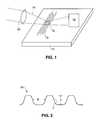
This problem is illustrated in FIG. 1 which shows awafer 10 having formed thereon a number ofconductive lines 12. Aprobe beam 14 is shown focused by alens 20 onto the sample at aspot 16. The reflected beam is measured by aphotodetector 18. As can be seen,spot 16 overlapsmultiple lines 12 and therefore cannot be used to measure distances between lines or the thickness of the lines themselves.
To overcome this problem, sophisticated software programs have been developed which analyze the reflected probe beam in terms of a scattering model. More specifically, it is understood that critical dimensions or feature profiles on the surface of the wafer will cause some level of scattering of the reflected probe beam light. If this scattering pattern is analyzed, information about the critical dimensions can be derived. This approach has been called specular scatterometry. The algorithms use various forms of modeling approaches including treating the lines as an optical grating. These algorithms attempt to determine the geometry of the periodic structure.
FIG. 2 schematically illustrates the geometry of one type ofperiodic structure 24. This periodic structure can be analyzed in terms of the width W between the features and the depth D of the grooves. In addition, the shape or profile P of the side walls of the features can also be analyzed by the current algorithms operating on the analytical data.
To date, these analytical programs have been used with data taken from conventional spectroscopic reflectometry or spectroscopic ellipsometry devices. In addition, some efforts have been made to extend this approach to analyzing data from simultaneous multiple angle of incidence systems. In these systems, the spot size is relatively small, but still larger than the individual features of the periodic structure. Paradoxically, where the features are only slightly smaller than the spot size, analysis through scatterometry is difficult since not enough of the repeating structure is covered by the spot. Accordingly, it would be desirable to modify the system so a sufficient number of individual features are measured so a good statistically based, scatterometry analysis can be performed.
The assignee of the subject invention has previously developed simultaneous multiple angle of incidence measurement tools which have been used to derive characteristics of thin films on semiconductor wafers. It is believed that data from the same type of tools can be used with an appropriate scattering model analysis to determine critical dimensions and feature profiles on semiconductors.
Detailed descriptions of assignee's simultaneous multiple angle of incidence devices can be found in the following U.S. Pat. Nos.: 4,999,014; 5,042,951; 5,181,080; 5,412,473 and 5,596,411, all incorporated herein by reference. The assignee manufactures a commercial device, the Opti-Probe which takes advantage of some of these simultaneous, multiple angle of incidence systems. A summary of all of the metrology devices found in the Opti-Probe can be found in PCT application WO/9902970, published Jan. 21, 1999.
One of these simultaneous multiple angle of incidence tools is marketed by the assignee under the name beam profile reflectometer (BPR). In this tool, a probe beam is focused with a strong lens so that the rays within the probe beam strike the sample at multiple angles of incidence. The reflected beam is directed to an array photodetector. The intensity of the reflected beam as a function of radial position within the beam is measured and includes not only the specularly reflected light but also the light that has been scattered into that detection angle from all of the incident angles as well. Thus, the radial positions of the rays in the beam illuminating the detector correspond to different angles of incidence on the sample plus the integrated scattering from all of the angles of incidence contained in the incident beam. In this manner, simultaneous multiple angle of incidence reflectometry can be performed.
Another tool used by the assignee is known as beam profile ellipsometry. In one embodiment as shown and described in U.S. Pat. No. 5,042,951, the arrangement is similar to that described for BPR except that additional polarizers and/or analyzers are provided. In this arrangement, the change in polarization state of the various rays within the probe beam are monitored as a function of angle of incidence.
It is believed that the data generated by either of these tools could be used to appropriately model and analyze critical dimensions and feature profiles on semiconductors.
The lens used to create the probe beam spot from a laser source in the above two simultaneous multiple angle of incidence systems is typically larger than the distance between adjacent features of the periodic structure of interest. However, in order to provide statistically significant information, it is desirable that information be collected from at least twenty or more of the repeating features. One method of achieving this goal is to increase the spot size of the probe beam. Such an approach is described in U.S. Pat. No. 5,889,593 incorporated by reference. In this patent, a proposal is made to include an optical imaging array for breaking up the coherent light bundles to create a larger spot.
It is believed the latter approach is not desirable because of the additional complexity it introduces into the measurement. Ideally, when attempting to analyze a periodic structure (e.g., a periodic critical dimension array) it is desirable to have no additional periodicities in the measurement system between the source and detector. Multiple periodic signals are more difficult to analyze and are often plagued with added uncertainty and ambiguity with respect to extracting parameters associated with any of the constituent components.
In accordance with the subject invention, the requirement for increasing the area over which measurements are taken is achieved in two different ways. In the first approach, the probe beam spot is scanned over the wafer until a sufficient amount of data are taken. Once the data are taken, a spatial averaging algorithm is utilized. Spatial averaging is discussed in U.S. patent application, Ser. No. 09/658,812, filed Sep. 11, 2000 and incorporated herein by reference. In another approach, the probe beam is generated by an incoherent or white light source. When incoherent light is focused by a lens, the spot size will be significantly larger than with a laser. No separate imaging array needs to be included to break up the coherence of the light as in the prior art. In such a system, a monochrometer could be located between the light source and the detector to permit measurement of a narrow band of wavelengths. The wavelength selected can be matched to the type of sample being inspected in order to obtain the most statistically relevant data. In addition, it would also be possible to scan the monochrometer in order to capture data at multiple wavelengths. It would also be possible to measure multiple wavelengths simultaneously as described in U.S. Pat. No. 5,412,473.
Alternatively or in addition, the measurement data which can be obtained from two or more metrology devices of the type described in the above identified PCT application, could be used to advance this analysis. As more of these metrology devices are added, the ability to unambiguously distinguish features increases. Thus, it is within the scope of the subject invention to utilize either or both of a simultaneous multiple angle of incidence spectrometer or ellipsometer along with one or more of spectroscopic reflectometry, spectroscopic ellipsometry or absolute ellipsometry tools with the latter two being deployed in a manner that maximizes the information content of the measurement. For example, with a rotating compensator spectroscopic ellipsometer one measures both the sign and magnitude of the ellipsometric phase while in more standard configurations, e.g., a rotating polarizer/rotating analyzer, only the magnitude or phase can be measured.
An example of an analytical approach for evaluating critical dimensions using data from a broadband reflectometer is described in “In-situ Metrology for Deep Ultraviolet Lithography Process Control,” Jakatdar et. al. SPIE Vol. 3332, pp. 262-270 1998. An example of using a spectroscopic ellipsometer equipment for CD metrology is described in, “Specular Spectroscopic Scatterometry in DUV Lithography, SPIE Vol. 3677, pp 159-168, from the SPIE Conference on Metrology, Inspection and Process Control for Microlithography XIII, Santa Clara, Calif., March 1999.
Further and related information measuring critical dimensions can be found in U.S. Pat. No. 5,830,611 and 5,867,276, incorporated herein by reference.
FIG. 1 is schematic diagram illustrating the optical measurement of periodic structure on a sample.
FIG. 2 is a cross-sectional illustration of the type of periodic structure which can be measured in accordance with the subject invention.
FIG. 3 is a schematic diagram of an apparatus for performing the method of the subject invention.
FIG. 4 is a schematic diagram illustrating an alternate embodiment of the subject apparatus for performing spectroscopic measurements.
Turning to FIG. 3, a basic schematic of simultaneous multiple angle ofincidence apparatus 30 is illustrated, Further details about such a device are described in U.S. Pat. Nos. 4,999,014; 5,042,951; 5,159,412 and 5,412,473 all incorporated herein by reference. As noted above, the assignee's Opti-Probe device incorporates portions of this technology and markets the measurement subsystem under the trademark Beam Profile Reflectometry or BPR. In the past, the BPR technology was utilized primarily to analyze the characteristics of thin films formed on semiconductors. This disclosure is directed to using the measurements which can be obtained from this type of system to evaluate the geometry of periodic structures formed on semiconductors.
The basic measurement system includes alight source 32 for generating aprobe beam 34. The light source can be a laser for generating a coherent beam of radiation. Laser diodes are suitable laser sources for this application. If the output of the laser is not itself polarized, a separate linear polarizer can be provided. As discussed below,light source 32 can also be a polychromatic or white light source for generating a probe beam with a plurality of wavelengths.
Theprobe beam 34 is focused onto thesample 10 using alens 40 in a manner so that the rays within the probe beam create a spread of angles of incidence. In the preferred embodiment, the beam is directed normal to the surface but can be arranged off-axis as illustrated in U.S. Pat. No. 5,166,752, incorporated by reference.Lens 40 is preferably a high numerical aperture lens (on the order of 0.90) to create angles of incidence from zero to about 70 degrees. The lens creates rays having predominantly S-polarized light along one axis and predominantly P-polarized light along an orthogonal axis. At intermediate angles, the polarization is mixed.
In order to obtain data sufficient to perform an accurate evaluation, it is preferable that the probe beam collect information from at least 20 repeating features in the pattern. If theprobe beam spot 42 is not sufficiently large, than it would be desirable to scan the probe beam over the surface of the sample in the region of the periodic structure. This can be accomplished by moving anX-Y stage 44 upon which the sample rests. It would also be possible to provide scanning capability to the probe beam itself. Scanning would preferably be in a direction perpendicular to the parallel features of the periodic structure. Data is generated as a function of the position of the probe beam spot with respect to the features of the periodic structure. Where the sample is scanned, the data is analyzed as discussed above and further clarified using a spatial averaging algorithm. In this spatial averaging approach, the data from points in the scan are filtered by a repeated sequence of averaging and outlier exclusions where the outliers are defined by their differences with respect to signal levels and symmetry properties. The result of this process leads to data that are equivalent to those taken with an incoherent source illuminating an area the same as that scanned in the spatial averaging approach.
The reflected/scattered beam passes back up through thelens 40 which collimates the beam. The reflected beam is redirected by a splitter to animaging lens 48.Lens 48 magnifies and relays an image of the sample at the focal plane of the lens. Aspatial filter 50 having an aperture is placed in the focal plane of thelens 48 for controlling size of the area of the sample which is measured.
The probe beam is than passed through a 50—50 splitter and directed to twophotodetectors
The output signals from the detector arrays are supplied to theprocessor 60. Processor will analyze the signals based on algorithm which considers the reflected and scattered light such as a rigorous coupled wave analysis. The selected algorithm will correlate the variation in reflectivity as a function of angle of incidence with the geometry of the periodic structure. Such scattered light theoretical models are well known in the literature. In addition to the articles cited above, further examples can be found in the following articles which are cited by way of example. Those skilled in the art of analyzing signals diffracted from periodic structures will understand that there are many other approaches which can be utilized. It should be noted that since this approach obtains measurements at multiple angles of incidence, higher order diffraction effects may be collected and considered.
Prior articles:
1. “Optical Etch-Rate Monitoring: Computer Simulation of Reflectance,” Heimann and Schultz,J. Electrochem. Soc: Solid State Science and Technology,April 1984, Vol. 131, No. 4, page 881
2. “Optical Etch-Rate Monitoring Using Active Device Areas: Lateral Interference Effects”, Heimann,J. Electrochem. Soc: Solid State Science and Technology,August 1985, Vol. 132, No. 8, page 2003.
3. “Scatterometry for 0.24 micron-0.70 micron developed photoresist metrology,” Murnane et. al.SPIE,Vol. 2439, page 427 (1995).
4. “Multi-Parameter Process metrology using scatterometry,” Raymond et. al.SPIEVol. 2638, page 84 (1995).
5. “Specular Spectral Profilometry on Metal Layers,” Bao et. al,SPIEVol 3998 (2000), page 882.
The type of analysis will depend on the application. For example, when used for process control, either in situ or near real time, the processor can compare the detected signals to an expected set of signals corresponding to the desired geometry of the periodic structure. If the detected signals do not match the expected signals, it is an indication that the process is not falling within the specified tolerances and should be terminated and investigated. In this approach, no sophisticated real time analysis of the signals is necessary.
As is known in the art, the reflected output signals at multiple angles of incidence can be more rigorously analyzed to determine the specific geometry of the periodic structure. While there are a number of different approaches, most have certain traits in common. More specifically, the analytical approach will typically start with a theoretical “best guess” of the geometry of the measured structure. Using Fresnel equations covering both the reflection and scattering of light, calculations are made to determine what the expected measured output signals would be at different angles of incidence for the theoretical geometry. These theoretical output signals are compared to the actual measured output signals and the differences noted. Based on the differences, the processor will generate a new set of theoretical output signals corresponding to a different theoretical periodic structure. Another comparison is made to determine if the theoretical signals are closer to the actual measured signals. These generation and comparison steps are repeated until the differences between the theoretically generated data and the actually measured data are substantially minimized. Once the differences have been minimized, the theoretical periodic structure corresponding to the best fit theoretical data is assumed to represent the actual periodic structure.
This minimization procedure can be carried out with a conventional least squares fitting routine such as a Levenberg-Marquardt algorithm. It would also be possible to use a genetic algorithm. (See, U.S. Pat. No. 5,953,446.)
In the past, this type of rigorous analysis was limited to the research environment, since the calculations necessary to determine the periodic structure was extremely complex and time consuming. However, with advent of faster and parallel processing technologies, it is believed that such an analytical approach could be used in a real time analysis.
One method for reducing the computer processing time during measurement activities is to create a library of possible solutions in advance. (See the Jakatdar articles, cited above). In this approach, a range of possible periodic structures and their associated theoretical output signals are generated in advance using the Fresnel equations as discussed above. The results are stored as a library in a processor memory. During the measurement activities, the actual measured signals are compared with sets of theoretically generated output signals stored in the library. The periodic structure associated with the set of theoretical signals which most closely matches the actual measured data is assumed to most closely represent the geometry of the measured periodic structure.
The simultaneous multiple angle approach is not limited to reflectometry. As noted in U.S. Pat. Nos. 5,042,951 and 5,166,752 (incorporated herein by reference), it is also possible to obtain ellipsometric measurements corresponding to W and A simultaneously at multiple angles of incidence. To obtain such measurements, some additional optical elements should be added to the device of FIG.3. For example, a polarizer66 (shown in phantom) is desirable to accurately predetermine the polarization state of the probe beam. On the detection side, an analyzer68 (also shown in phantom) is provided to aid in analyzing the change in polarization state of the probe beam due to interaction with the sample. The optical components of the analyzer can be of any type typically used in an ellipsometer such as a polarizer or a retarder. The ellipsometric output signals are analyzed in a fashion similar to the prior art approaches for using ellipsometric data to evaluate the geometry of periodic structures.
Another approach to increasing the size of the probe beam spot is to use an incoherent source for the probe beam. Such an incoherent source can include a variety of well known spectral line or broad band sources. If a spectral line light source is used, some modest level of narrow pass filtering may be desirable. Such a filter could be located either before the sample or before the detector as indicated inphantom lines
It would also be possible to use a broadband or white light source generating a polychromatic beam. In this situation, the wavelength selective filter could be in the form of a conventional monochrometer. A monochrometer, which typically includes a dispersive element and a slit, functions to transmit a narrow band of wavelengths. The system could be arranged to take measurements at only one wavelength or in a series of sequential wavelengths as the monochrometer is tuned. The use of an incoherent light source would fill the field of view on the sample (typically 100 microns or more for a 0.9 NA microscope objective). The actual measurement spot size is controlled by an aperture that can be varied in size as needed for the particular measurement in question. Such variable spatial filtering is described in U.S. Pat. No. 5,412,473.
It would also be possible to set up a system where both the multiple angle and multiple wavelength information is obtained simultaneously. Such a detection scheme is also described in detail in U.S. Pat. No. 5,412,473, incorporated by reference. This detection scheme is briefly described herein with reference to FIG.4.
In this embodiment, theprobe beam 34ais a broadband polychromatic beam generated by awhite light source 32agenerating an incoherent probe beam. There are a number of white light sources available such as tungsten or deuterium bulbs. Theprobe beam 34ais focused on the sample withlens 40. Upon reflection, the probe beam is passed throughrelay lens 48 andspatial filter 50 in the manner described above. In addition, the beam is passed through afilter 70 having anslit 72 located in the relay image plane of the exit pupil oflens 40.Lens 48 also serves to relay this image. The slit is dimensioned so that image transmitted to thedetector 74 will be on the order of the dimensions of a row ofdetector elements 76.
After the beam passes through the slit, it is dispersed as a function of wavelength byelement 80. Any conventional wavelength dispersing element can be used, such as a grating, prism or holographic plate.
The dispersed beam is directed to the detector which is a two dimensional array of photodiodes. A CCD element could also be used. Theslit 72 is oriented perpendicular to the axis of the dispersion of the light. In this matter, each horizontal row of elements on thearray 74 will measure a narrow wavelength band of light. Each of the elements in each row correspond to different angles of incidence. Thus, the output of thedetector 74 will simultaneously produce data for multiple wavelengths and multiple angles of incidence. As noted in U.S. Pat. No. 5,412,473, this type of detection system can be used for either reflectometry or ellipsometry measurements.
It is also within the scope of the subject invention to combine these measurements with other measurements that might be available from a composite tool. As noted above, the assignee's Opti-Probe device (as described in WO 99/02970) has multiple measurement technologies in addition to the Beam Profile Reflectometry system. These other technologies include broadband reflectometry and broadband ellipsometry. The output from these additional modules can be used in combination with the BPR signals to more accurately evaluate the geometry of the periodic structures.
In summary, there has been described a method and apparatus for evaluating relatively small periodic structures formed on semiconductor samples. In this approach, a light source generates a probe beam which is directed to the sample. In one embodiment, the light source generates incoherent light. A lens is used to focus the probe beam on the sample in a manner so that rays within the probe beam create a spread of angles of incidence. The size of the probe beam spot on the sample is larger than the spacing between the features of the periodic structure so some of the light is scattered from the structure. A detector is provided for monitoring the reflected and scattered light. The detector includes multiple detector elements arranged so that multiple output signals are generated simultaneously and correspond to multiple angles of incidence. The output signals are supplied to a processor which analyzes the signals according to a scattering model which permits evaluation of the geometry of the periodic structure. Both single and multiple wavelength embodiments are disclosed.
While the subject invention has been described with reference to a preferred embodiment, various changes and modifications could be made therein, by one skilled in the art, without varying from the scope and spirit of the subject invention as defined by the appended claims.
Claims (84)
1. An apparatus for evaluating the geometry of a periodic structure formed on a sample comprising:
an incoherent light source for generating a probe beam;
an optical element for focusing the probe beam to a spot on the sample surface in a manner so that the rays within the probe beam create a spread of angles of incidence and wherein the spot size on the sample is larger than the spacing between the features of the periodic structure so that the probe beam is diffracted upon reflection;
a detector array for monitoring the light of the probe beam diffracted from the periodic structure, said detector array simultaneously generating a plurality of independent output signals corresponding to a plurality of different angles of incidence; and
a processor for evaluating the geometry of the periodic structure on the sample based on the output signals generated by the detector.
2. An apparatus as recited inclaim 1 wherein said light source is polychromatic.
3. An apparatus as recited inclaim 2 further including a wavelength selective filter located between the light source and the detector array.
4. An apparatus as recited inclaim 3 wherein said wavelength selective filter is a monochrometer.
5. An apparatus as recited inclaim 4 wherein the detector array generates output signals corresponding to a plurality of wavelengths.
6. An apparatus as recited inclaim 2 further including a dispersive element for spreading the wavelengths of light in the probe beam being diffracted from the sample and wherein the detector array is arranged to simultaneously generate output signals at multiple wavelengths.
7. An apparatus as recited inclaim 1 wherein at least twenty repetitive features of the periodic structure are imaged by the detector array.
8. An apparatus as recited inclaim 1 wherein the size of the probe beam spot is illuminates at least twenty repetitive features of the periodic structure.
9. An apparatus as recited inclaim 1 further including an analyzer and wherein the processor determines the change in polarization state of the rays within the probe beam to evaluate the geometry of the periodic structure on the sample.
10. An apparatus as recited inclaim 1 wherein the optical element for focusing the probe beam is a lens.
11. An apparatus as recited inclaim 1 wherein the probe beam is directed substantially normal to the sample.
12. An apparatus as recited inclaim 1 wherein the processor functions to generate a set of theoretical output signals based on a theoretical profile of the periodic structure and wherein the theoretical output signals are compared with the actual output signals and thereafter, the processor generates another set of theoretical output signals based on the comparison and using a different theoretical profile of the periodic structure and wherein the comparison and generation steps are repeated until the differences between the theoretical output signals and the actual output signals are minimized.
13. An apparatus as recited inclaim 1 wherein the processor compares the output signals to a set of previously generated theoretical output signals to find the closest match and wherein each one of the set of previously generated output signals corresponds to a different possible geometry of the periodic structure.
14. An apparatus as recited inclaim 1 wherein the processor compares the output signals to a predetermined set of output signals to determine if a process is within specified tolerances.
15. An apparatus as recited inclaim 1 wherein the probe beam spot is scanned with respect to the periodic structure and output signals are generated as a function of position.
16. An apparatus as recited inclaim 15 wherein said processor filters the output signals generated during the scan using a repeated sequence of averaging and outlier exclusions wherein the outliers are defined by their differences with respect to signal levels and symmetry properties.
17. An apparatus for evaluating the geometry of a periodic structure formed on a sample comprising:
an incoherent light source for generating a probe beam;
an optical element for focusing the probe beam to a spot on the sample surface in a manner so that the rays within the probe beam create a spread of angles of incidence and wherein the spot size on the sample is larger than the spacing between the features of the periodic structure so that the probe beam is diffracted upon reflection;
detector means for monitoring the light of the probe beam diffracted from the periodic structure, said detector means for simultaneously generating a plurality of independent output signals corresponding to a plurality of different angles of incidence; and
a processor for evaluating the geometry of the periodic structure on the sample based on the output signals generated by the detector.
18. An apparatus as recited inclaim 17 wherein said light source is polychromatic.
19. An apparatus as recited inclaim 18 further including a wavelength selective filter located between the light source and the detector means.
20. An apparatus as recited inclaim 19 wherein said wavelength selective filter is a monochrometer.
21. An apparatus as recited inclaim 20 wherein the detector means generates output signals corresponding to a plurality of wavelengths.
22. An apparatus as recited inclaim 18 further including a dispersive element for spreading the wavelengths of light in the probe beam being diffracted from the sample and wherein the detector means is arranged to simultaneously generate output signals at multiple wavelengths.
23. An apparatus as recited inclaim 17 wherein at least twenty repetitive features of the periodic structure are imaged by the detector means.
24. An apparatus as recited inclaim 17 wherein the size of the probe beam spot is illuminates at least twenty repetitive features of the periodic structure.
25. An apparatus as recited inclaim 17 further including an analyzer and wherein the processor determines the change in polarization state of the rays within the probe beam to evaluate the geometry of the periodic structure on the sample.
26. An apparatus as recited inclaim 17 wherein the optical element for focusing the probe beam is a lens.
27. An apparatus as recited inclaim 17 wherein the probe beam is directed substantially normal to the sample.
28. An apparatus as recited inclaim 17 wherein the processor functions to generate a set of theoretical output signals based on a theoretical profile of the periodic structure and wherein the theoretical output signals are compared with the actual output signals and thereafter, the processor generates another set of theoretical output signals based on the comparison and using a different theoretical profile of the periodic structure and wherein the comparison and generation steps are repeated until the differences between the theoretical output signals and the actual output signals are minimized.
29. An apparatus as recited inclaim 17 wherein the processor compares the output signals to a set of previously generated theoretical output signals to find the closest match and wherein each one of the set of previously generated output signals corresponds to a different possible geometry of the periodic structure.
30. An apparatus as recited inclaim 17 wherein the processor compares the output signals to a predetermined set of output signals to determine if a process is within specified tolerances.
31. An apparatus as recited inclaim 17 wherein the probe beam spot is scanned with respect to the periodic structure and output signals are generated as a function of position.
32. An apparatus as recited inclaim 31 wherein said processor filters the output signals generated during the scan using a repeated sequence of averaging and outlier exclusions wherein the outliers are defined by their differences with respect to signal levels and symmetry properties.
33. A method for evaluating the geometry of a periodic structure formed on a sample comprising the steps of:
focusing a probe beam of incoherent radiation to a spot on the sample surface in a manner so that the rays within the probe beam create a spread of angles of incidence and wherein the spot size on the sample is larger than the spacing between the features of the periodic structure so that the probe beam is diffracted upon reflection;
monitoring the light of the probe beam diffracted from the periodic structure and simultaneously generating a plurality of independent output signals corresponding to a plurality of different angles of incidence; and
evaluating the geometry of the periodic structure on the sample based on the output signals.
34. A method as recited inclaim 33 wherein probe beam is generated by a polychromatic light source.
35. A method as recited inclaim 34 wherein a wavelength selective is filter located in the path of the probe beam.
36. A method as recited inclaim 35 wherein said wavelength selective filter is a monochrometer.
37. A method as recited inclaim 34 wherein the output signals correspond to a plurality of wavelengths.
38. A method as recited inclaim 37 the output signals are generated at multiple wavelengths simultaneously.
39. A method as recited inclaim 33 wherein the monitored probe beam light has illuminated at least twenty repetitive features of the periodic structure.
40. A method as recited inclaim 33 wherein the size of the probe beam spot illuminates at least twenty repetitive features of the periodic structure.
41. A method as recited inclaim 33 wherein the probe beam is passed through an analyzer and wherein the change in polarization state of the rays within the probe beam are monitored.
42. A method as recited inclaim 33 wherein the step of evaluating the geometry of the periodic structure includes generating a set of theoretical output signals based on a theoretical profile of the periodic structure and wherein the theoretical output signals are compared with the actual output signals and thereafter generating another set of theoretical output signals based on the comparison and using a different theoretical profile of the periodic structure and wherein the comparison and generation steps are repeated until the differences between the theoretical output signals and the actual output signals are minimized.
43. A method as recited inclaim 33 wherein the step of evaluating the geometry of the periodic structure includes comparing the output signals to a set of previously generated theoretical output signals to find the closest match and wherein each one of the set of previously generated output signals corresponds to a different possible geometry of the periodic structure.
44. A method as recited inclaim 33 wherein the step of evaluating the geometry of the periodic structure includes comparing the output signals to a predetermined set of output signals to determine if a process is within specified tolerances.
45. A method as recited inclaim 33 wherein the probe beam spot is scanned with respect to the periodic structure and output signals are generated as a function of position.
46. A method as recited inclaim 45 wherein the step of evaluating the geometry of the periodic structure includes filtering the output signals generated during the scan using a repeated sequence of averaging and outlier exclusions wherein the outliers are defined by their differences with respect to signal levels and symmetry properties.
47. An apparatus for evaluating the geometry of a periodic structure formed on a sample comprising:
a light source for generating a probe beam;
an optical element for focusing the probe beam to a spot on the sample surface in a manner so that the rays within the probe beam create a spread of angles of incidence and wherein the spot size on the sample is larger than the spacing between the features of the periodic structure so that the probe beam is diffracted upon reflection;
a detector array for monitoring the light of the probe beam diffracted from the periodic structure, said detector array simultaneously generating a plurality of independent output signals corresponding to a plurality of different angles of incidence;
a movable stage for supporting the sample and permitting relative movement between the sample and the probe beam so that output signals can be generating as a function of position; and
a processor for evaluating the geometry of the periodic structure on the sample based on the output signals generated by the detector.
48. An apparatus as recited inclaim 47 wherein the light source is a laser beam.
49. An apparatus as recited inclaim 47 wherein said processor filters the output signals using a repeated sequence of averaging and outlier exclusions wherein the outliers are defined by their differences with respect to signal levels and symmetry properties.
50. An apparatus as recited inclaim 47 wherein said light source is an incoherent, polychromatic source.
51. An apparatus as recited inclaim 50 further including a wavelength selective filter located between the light source and the detector array.
52. An apparatus as recited inclaim 51 wherein said wavelength selective filter is a monochrometer.
53. An apparatus as recited inclaim 52 wherein the detector array generates output signals corresponding to a plurality of wavelengths.
54. An apparatus as recited inclaim 50 further including a dispersive element for spreading the wavelengths of light in the probe beam being diffracted from the sample and wherein the detector array is arranged to simultaneously generate output signals at multiple wavelengths.
55. An apparatus as recited inclaim 47 wherein at least twenty repetitive features of the periodic structure are imaged by the detector array.
56. An apparatus as recited inclaim 47 further including an analyzer and wherein the processor determines the change in polarization state of the rays within the probe beam to evaluate the geometry of the periodic structure on the sample.
57. An apparatus as recited inclaim 47 wherein the optical element for focusing the probe beam is a lens.
58. An apparatus as recited inclaim 47 wherein the probe beam is directed substantially normal to the sample.
59. An apparatus as recited inclaim 47 wherein the processor functions to generate a set of theoretical output signals based on a theoretical profile of the periodic structure and wherein the theoretical output signals are compared with the actual output signals and thereafter, the processor generates another set of theoretical output signals based on the comparison and using a different theoretical profile of the periodic structure and wherein the comparison and generation steps are repeated until the differences between the theoretical output signals and the actual output signals are minimized.
60. An apparatus as recited inclaim 47 wherein the processor compares the output signals to a set of previously generated theoretical output signals to find the closest match and wherein each one of the set of previously generated output signals corresponds to a different possible geometry of the periodic structure.
61. An apparatus as recited inclaim 47 wherein the processor compares the output signals to a predetermined set of output signals to determine if a process is within specified tolerances.
62. A method for evaluating the geometry of a periodic structure formed on a sample comprising the steps of:
focusing a probe beam of radiation to a spot on the sample surface in a manner so that the rays within the probe beam create a spread of angles of incidence and wherein the spot size on the sample is larger than the spacing between the features of the periodic structure so that the probe beam is diffracted upon reflection;
translating the sample with respect to the probe beam;
monitoring the light of the probe beam diffracted from the periodic structure and simultaneously generating a plurality of independent output signals corresponding to a plurality of different angles of incidence as a function of position of the probe beam with respect to the periodic structure; and
evaluating the geometry of the periodic structure on the sample based on the output signals.
63. A method as recited inclaim 62 , wherein the probe beam is generated by a laser.
64. A method as recited inclaim 62 wherein the step of evaluating the geometry of the periodic structure includes filtering the output signals generated using a repeated sequence of averaging and outlier exclusions wherein the outliers are defined by their differences with respect to signal levels and symmetry properties.
65. A method as recited inclaim 62 , wherein the probe beam is generated by an incoherent polychromatic source.
66. A method as recited inclaim 65 wherein a wavelength selective filter is located in the path of the probe beam.
67. A method as recited inclaim 66 wherein said wavelength selective filter is a monochrometer.
68. A method as recited inclaim 65 wherein the output signals correspond to a plurality of wavelengths.
69. A method as recited inclaim 68 the output signals are generated at multiple wavelengths simultaneously.
70. A method as recited inclaim 62 wherein the monitored probe beam light has illuminated at least twenty repetitive features of the periodic structure.
71. A method as recited inclaim 62 wherein the probe beam is passed through an analyzer and wherein the change in polarization state of the rays within the probe beam are monitored.
72. A method as recited inclaim 62 wherein the step of evaluating the geometry of the periodic structure includes generating a set of theoretical output signals based on a theoretical profile of the periodic structure and wherein the theoretical output signals are compared with the actual output signals and thereafter generating another set of theoretical output signals based on the comparison and using a different theoretical profile of the periodic structure and wherein the comparison and generation steps are repeated until the differences between the theoretical output signals and the actual output signals are minimized.
73. A method as recited inclaim 62 wherein the step of evaluating the geometry of the periodic structure includes comparing the output signals to a set of previously generated theoretical output signals to find the closest match and wherein each one of the set of previously generated output signals corresponds to a different possible geometry of the periodic structure.
74. A method as recited inclaim 62 wherein the step of evaluating the geometry of the periodic structure includes comparing the output signals to a predetermined set of output signals to determine if a process is within specified tolerances.
75. An apparatus for evaluating the geometry of a periodic structure formed on a sample comprising:
a light source for generating a probe beam;
an optical element for focusing the probe beam to a spot on the sample surface in a manner so that the rays within the probe beam create a spread of angles of incidence and wherein the spot size on the sample is larger than the spacing between the features of the periodic structure so that the probe beam is diffracted upon reflection;
detector means for monitoring the light of the probe beam diffracted from the periodic structure, said detector means simultaneously generating a plurality of independent output signals corresponding to a plurality of different angles of incidence;
means for create relative movement between the sample and the probe beam so that output signals can be generating as a function of position; and
a processor for evaluating the geometry of the periodic structure on the sample based on the output signals generated by the detector.
76. An apparatus as recited inclaim 75 wherein the light source is a laser beam.
77. An apparatus as recited inclaim 76 wherein said processor filters the output signals using a repeated sequence of averaging and outlier exclusions wherein the outliers are defined by their differences with respect to signal levels and symmetry properties.
78. An apparatus as recited inclaim 75 wherein said light source is an incoherent, polychromatic source.
79. An apparatus as recited inclaim 78 further including a wavelength selective filter located between the light source and the detector means.
80. An apparatus as recited inclaim 78 wherein the detector means generates output signals corresponding to a plurality of wavelengths.
81. An apparatus as recited inclaim 75 further including an analyzer and wherein the processor determines the change in polarization state of the rays within the probe beam to evaluate the geometry of the periodic structure on the sample.
82. An apparatus as recited inclaim 75 wherein the processor functions to generate a set of theoretical output signals based on a theoretical profile of the periodic structure and wherein the theoretical output signals are compared with the actual output signals and thereafter, the processor generates another set of theoretical output signals based on the comparison and using a different theoretical profile of the periodic structure and wherein the comparison and generation steps are repeated until the differences between the theoretical output signals and the actual output signals are minimized.
83. An apparatus as recited inclaim 75 wherein the processor compares the output signals to a set of previously generated theoretical output signals to find the closest match and wherein each one of the set of previously generated output signals corresponds to a different possible geometry of the periodic structure.
84. An apparatus as recited inclaim 75 wherein the processor compares the output signals to a predetermined set of output signals to determine if a process is within specified tolerances.
Priority Applications (5)
| Application Number | Priority Date | Filing Date | Title |
|---|---|---|---|
| US09/818,703US6429943B1 (en) | 2000-03-29 | 2001-03-27 | Critical dimension analysis with simultaneous multiple angle of incidence measurements |
| US10/150,032US6654131B2 (en) | 2000-03-29 | 2002-05-17 | Critical dimension analysis with simultaneous multiple angle of incidence measurements |
| US10/658,176US6829057B2 (en) | 2000-03-29 | 2003-09-09 | Critical dimension analysis with simultaneous multiple angle of incidence measurements |
| US10/973,703US6972852B2 (en) | 2000-03-29 | 2004-10-26 | Critical dimension analysis with simultaneous multiple angle of incidence measurements |
| US11/231,638US7248375B2 (en) | 2000-03-29 | 2005-09-21 | Critical dimension analysis with simultaneous multiple angle of incidence measurements |
Applications Claiming Priority (2)
| Application Number | Priority Date | Filing Date | Title |
|---|---|---|---|
| US19289900P | 2000-03-29 | 2000-03-29 | |
| US09/818,703US6429943B1 (en) | 2000-03-29 | 2001-03-27 | Critical dimension analysis with simultaneous multiple angle of incidence measurements |
Related Child Applications (1)
| Application Number | Title | Priority Date | Filing Date |
|---|---|---|---|
| US10/150,032ContinuationUS6654131B2 (en) | 2000-03-29 | 2002-05-17 | Critical dimension analysis with simultaneous multiple angle of incidence measurements |
Publications (1)
| Publication Number | Publication Date |
|---|---|
| US6429943B1true US6429943B1 (en) | 2002-08-06 |
Family
ID=26888485
Family Applications (5)
| Application Number | Title | Priority Date | Filing Date |
|---|---|---|---|
| US09/818,703Expired - LifetimeUS6429943B1 (en) | 2000-03-29 | 2001-03-27 | Critical dimension analysis with simultaneous multiple angle of incidence measurements |
| US10/150,032Expired - LifetimeUS6654131B2 (en) | 2000-03-29 | 2002-05-17 | Critical dimension analysis with simultaneous multiple angle of incidence measurements |
| US10/658,176Expired - LifetimeUS6829057B2 (en) | 2000-03-29 | 2003-09-09 | Critical dimension analysis with simultaneous multiple angle of incidence measurements |
| US10/973,703Expired - LifetimeUS6972852B2 (en) | 2000-03-29 | 2004-10-26 | Critical dimension analysis with simultaneous multiple angle of incidence measurements |
| US11/231,638Expired - LifetimeUS7248375B2 (en) | 2000-03-29 | 2005-09-21 | Critical dimension analysis with simultaneous multiple angle of incidence measurements |
Family Applications After (4)
| Application Number | Title | Priority Date | Filing Date |
|---|---|---|---|
| US10/150,032Expired - LifetimeUS6654131B2 (en) | 2000-03-29 | 2002-05-17 | Critical dimension analysis with simultaneous multiple angle of incidence measurements |
| US10/658,176Expired - LifetimeUS6829057B2 (en) | 2000-03-29 | 2003-09-09 | Critical dimension analysis with simultaneous multiple angle of incidence measurements |
| US10/973,703Expired - LifetimeUS6972852B2 (en) | 2000-03-29 | 2004-10-26 | Critical dimension analysis with simultaneous multiple angle of incidence measurements |
| US11/231,638Expired - LifetimeUS7248375B2 (en) | 2000-03-29 | 2005-09-21 | Critical dimension analysis with simultaneous multiple angle of incidence measurements |
Country Status (1)
| Country | Link |
|---|---|
| US (5) | US6429943B1 (en) |
Cited By (248)
| Publication number | Priority date | Publication date | Assignee | Title |
|---|---|---|---|---|
| US20020135783A1 (en)* | 2000-03-29 | 2002-09-26 | Jon Opsal | Critical dimension analysis with simultaneous multiple angle of incidence measurements |
| US20030002028A1 (en)* | 2001-05-17 | 2003-01-02 | Rice Bradley W. | Method and apparatus for determining target depth, brightness and size within a body region |
| US20030147086A1 (en)* | 2002-02-05 | 2003-08-07 | Allan Rosencwaig | Analysis of isolated and aperiodic structures with simultaneous multiple angle of incidence measurements |
| US6609086B1 (en)* | 2002-02-12 | 2003-08-19 | Timbre Technologies, Inc. | Profile refinement for integrated circuit metrology |
| US20030204326A1 (en)* | 2001-07-16 | 2003-10-30 | Jon Opsal | Real time analysis of periodic structures on semiconductors |
| US6642066B1 (en)* | 2002-05-15 | 2003-11-04 | Advanced Micro Devices, Inc. | Integrated process for depositing layer of high-K dielectric with in-situ control of K value and thickness of high-K dielectric layer |
| US20040004726A1 (en)* | 2002-07-05 | 2004-01-08 | Abdurrahman Sezginer | Overlay targets with isolated, critical-dimension features and apparatus to measure overplay |
| US20040008353A1 (en)* | 2002-07-09 | 2004-01-15 | Hanyou Chu | CD metrology analysis using a finite difference method |
| US20040021771A1 (en)* | 2002-07-16 | 2004-02-05 | Xenogen Corporation | Method and apparatus for 3-D imaging of internal light sources |
| US6697153B1 (en)* | 2002-02-20 | 2004-02-24 | Advanced Micro Devices, Inc. | Method and apparatus for analyzing line structures |
| US6713753B1 (en) | 2001-07-03 | 2004-03-30 | Nanometrics Incorporated | Combination of normal and oblique incidence polarimetry for the characterization of gratings |
| US20040105099A1 (en)* | 2002-11-20 | 2004-06-03 | Mehrdad Nikoonahad | System and method for characterizing three-dimensional structures |
| US20040136003A1 (en)* | 2003-01-09 | 2004-07-15 | Smith Walter Lee | Scatterometry for junction metrology |
| US20040169859A1 (en)* | 2003-02-28 | 2004-09-02 | Smith Walter Lee | Modulated scatterometry |
| US20040176928A1 (en)* | 2003-01-28 | 2004-09-09 | Johnson Kenneth C. | CD metrology method |
| US20040201836A1 (en)* | 2003-03-31 | 2004-10-14 | Yia-Chung Chang | Scatterometry for samples with non-uniform edges |
| US20040210402A1 (en)* | 2003-04-18 | 2004-10-21 | Jon Opsal | Global shape definition method for scatterometry |
| US20040212812A1 (en)* | 2002-06-18 | 2004-10-28 | Timbre Technologies, Inc. | Optical metrology of single features |
| US20040229471A1 (en)* | 2001-04-10 | 2004-11-18 | Ibrahim Abdulhalim | Periodic patterns and technique to control misalignment between two layers |
| US20040233436A1 (en)* | 2003-05-20 | 2004-11-25 | Haiming Wang | Self-calibrating beam profile ellipsometer |
| US20050009213A1 (en)* | 2003-06-27 | 2005-01-13 | Xinming Wang | Substrate processing method and apparatus |
| US20050014374A1 (en)* | 2002-12-31 | 2005-01-20 | Aaron Partridge | Gap tuning for surface micromachined structures in an epitaxial reactor |
| US20050041258A1 (en)* | 2002-03-13 | 2005-02-24 | Jon Opsal | Optical scatterometry of asymmetric lines and structures |
| US6867866B1 (en) | 2001-08-10 | 2005-03-15 | Therma-Wave, Inc. | CD metrology analysis using green's function |
| US20050105089A1 (en)* | 2001-08-28 | 2005-05-19 | Jon Opsal | Detector configurations for optical metrology |
| US6898537B1 (en)* | 2001-04-27 | 2005-05-24 | Nanometrics Incorporated | Measurement of diffracting structures using one-half of the non-zero diffracted orders |
| US20050134847A1 (en)* | 2003-12-19 | 2005-06-23 | Ray Hebert | Apparatus and method for optical characterization of a sample over a broadband of wavelengths with a small spot size |
| US20050134848A1 (en)* | 2003-12-19 | 2005-06-23 | Ray Hebert | Apparatus and method for optical characterization of a sample over a broadband of wavelengths while minimizing polarization changes |
| US20050140988A1 (en)* | 2003-12-29 | 2005-06-30 | Lee Dong-Gun | Optical critical dimension measurement equipment |
| US20050195412A1 (en)* | 2004-03-04 | 2005-09-08 | Jon Opsal | Systems and methods for immersion metrology |
| US6949462B1 (en) | 2002-04-04 | 2005-09-27 | Nanometrics Incorporated | Measuring an alignment target with multiple polarization states |
| US20050248763A1 (en)* | 2004-05-06 | 2005-11-10 | Aspnes David E | Normal incidence rotating compensator ellipsometer |
| US20050270524A1 (en)* | 2004-04-02 | 2005-12-08 | Wang David Y | Broadband wavelength selective filter |
| US6982793B1 (en) | 2002-04-04 | 2006-01-03 | Nanometrics Incorporated | Method and apparatus for using an alignment target with designed in offset |
| US6992764B1 (en) | 2002-09-30 | 2006-01-31 | Nanometrics Incorporated | Measuring an alignment target with a single polarization state |
| US20060033921A1 (en)* | 2004-08-16 | 2006-02-16 | Asml Netherlands B.V. | Method and apparatus for angular-resolved spectroscopic lithography characterization |
| US7061615B1 (en) | 2001-09-20 | 2006-06-13 | Nanometrics Incorporated | Spectroscopically measured overlay target |
| US20060158659A1 (en)* | 2005-01-20 | 2006-07-20 | Xavier Colonna De Lega | Interferometer for determining characteristics of an object surface |
| US7115858B1 (en) | 2000-09-25 | 2006-10-03 | Nanometrics Incorporated | Apparatus and method for the measurement of diffracting structures |
| US20060243912A1 (en)* | 2005-02-25 | 2006-11-02 | Accent Optical Technologies, Inc. | Apparatus and method for enhanced critical dimension scatterometry |
| US20060268153A1 (en)* | 2005-05-11 | 2006-11-30 | Xenogen Corporation | Surface contruction using combined photographic and structured light information |
| WO2006080902A3 (en)* | 2004-09-08 | 2007-03-08 | Accent Optical Tech Inc | Method and apparatus for determining line characteristics, e.g., line roughness, of microfeature components |
| US7206070B2 (en) | 2004-11-15 | 2007-04-17 | Therma-Wave, Inc. | Beam profile ellipsometer with rotating compensator |
| US20070091325A1 (en)* | 2005-01-07 | 2007-04-26 | Mehrdad Nikoonahad | Multi-channel optical metrology |
| US20070201017A1 (en)* | 2006-02-02 | 2007-08-30 | Jon Opsal | High resolution monitoring of CD variations |
| US20070219737A1 (en)* | 2006-03-17 | 2007-09-20 | Jon Opsal | Scatterometry multi-structure shape definition with multi-periodicity |
| US20070253908A1 (en)* | 2002-07-16 | 2007-11-01 | Xenogen Corporation | Fluorescent light tomography |
| US7298415B2 (en) | 2001-07-13 | 2007-11-20 | Xenogen Corporation | Structured light imaging apparatus |
| US20080036998A1 (en)* | 2006-08-10 | 2008-02-14 | Alex Salnik | Probe beam profile modulated optical reflectance system and methods |
| US20080052052A1 (en)* | 2006-08-24 | 2008-02-28 | Xenogen Corporation | Apparatus and methods for determining optical tissue properties |
| US20080170243A1 (en)* | 2007-01-15 | 2008-07-17 | Disco Corporation | Measuring apparatus for work held by chuck table, and laser beam machining apparatus |
| US7456975B2 (en) | 2003-09-15 | 2008-11-25 | Zygo Corporation | Methods and systems for interferometric analysis of surfaces and related applications |
| US7466429B2 (en) | 2003-03-06 | 2008-12-16 | Zygo Corporation | Profiling complex surface structures using scanning interferometry |
| US7522288B2 (en) | 2006-07-21 | 2009-04-21 | Zygo Corporation | Compensation of systematic effects in low coherence interferometry |
| US20090185168A1 (en)* | 2008-01-21 | 2009-07-23 | International Business Machines Corporation | Optical measurement using fixed polarizer |
| WO2009106253A1 (en)* | 2008-02-27 | 2009-09-03 | Asml Netherlands B.V. | Inspection method and apparatus, lithographic apparatus, lithographic processing cell and device manufacturing method |
| US7619746B2 (en) | 2007-07-19 | 2009-11-17 | Zygo Corporation | Generating model signals for interferometry |
| US7636168B2 (en) | 2005-10-11 | 2009-12-22 | Zygo Corporation | Interferometry method and system including spectral decomposition |
| US7684049B2 (en) | 2003-03-06 | 2010-03-23 | Zygo Corporation | Interferometer and method for measuring characteristics of optically unresolved surface features |
| US7700247B2 (en) | 2003-12-19 | 2010-04-20 | International Business Machines Corporation | Differential critical dimension and overlay metrology apparatus and measurement method |
| US20100245807A1 (en)* | 2009-03-30 | 2010-09-30 | Tokyo Electron Limited | Optimizing sensitivity of optical metrology measurements |
| US20100243860A1 (en)* | 2009-03-30 | 2010-09-30 | Tokyo Electron Limited | Controlling angle of incidence of multiple- beam optical metrology tools |
| US20100243859A1 (en)* | 2009-03-30 | 2010-09-30 | Tokyo Electron Limited | Apparatus for controlling angle of incidence of multiple illumination beams |
| US20100245819A1 (en)* | 2009-03-27 | 2010-09-30 | Guoguang Li | Method and apparatus for phase-compensated sensitivity-enhanced spectroscopy (PCSES) |
| US7812963B2 (en) | 2002-09-09 | 2010-10-12 | Zygo Corporation | Interferometry method for ellipsometry, reflectometry, and scatterometry measurements, including characterization of thin film structures |
| US20100277706A1 (en)* | 2004-08-16 | 2010-11-04 | Asml Netherlands B.V. | Method of Measurement, an Inspection Apparatus and a Lithographic Apparatus |
| US7869057B2 (en) | 2002-09-09 | 2011-01-11 | Zygo Corporation | Multiple-angle multiple-wavelength interferometer using high-NA imaging and spectral analysis |
| US7884947B2 (en) | 2005-01-20 | 2011-02-08 | Zygo Corporation | Interferometry for determining characteristics of an object surface, with spatially coherent illumination |
| US7889355B2 (en) | 2007-01-31 | 2011-02-15 | Zygo Corporation | Interferometry for lateral metrology |
| US20110069312A1 (en)* | 2009-09-03 | 2011-03-24 | Kla-Tencor Corporation | Metrology systems and methods |
| US7924435B2 (en) | 2006-12-22 | 2011-04-12 | Zygo Corporation | Apparatus and method for measuring characteristics of surface features |
| US7978337B2 (en) | 2007-11-13 | 2011-07-12 | Zygo Corporation | Interferometer utilizing polarization scanning |
| US7978338B2 (en) | 2008-11-26 | 2011-07-12 | Zygo Corporation | Compound reference interferometer |
| US8072611B2 (en) | 2007-10-12 | 2011-12-06 | Zygo Corporation | Interferometric analysis of under-resolved features |
| US8126677B2 (en) | 2007-12-14 | 2012-02-28 | Zygo Corporation | Analyzing surface structure using scanning interferometry |
| US8139232B2 (en) | 2006-07-27 | 2012-03-20 | Rudolph Technologies, Inc. | Multiple measurement techniques including focused beam scatterometry for characterization of samples |
| CN102706276A (en)* | 2012-05-24 | 2012-10-03 | 宁波大学 | Planar periodic structure measurement device and measurement method |
| US20120267802A1 (en)* | 2011-04-22 | 2012-10-25 | Guido De Boer | Position determination in a lithography system using a substrate having a partially reflective position mark |
| US20130116978A1 (en)* | 2011-11-03 | 2013-05-09 | Kla-Tencor Corporation | Secondary Target Design for Optical Measurements |
| US8468471B2 (en) | 2011-09-23 | 2013-06-18 | Kla-Tencor Corp. | Process aware metrology |
| WO2013109707A1 (en)* | 2012-01-17 | 2013-07-25 | Kla-Tencor Corporation | Apparatus and method of measuring roughness and other parameters of a structure |
| US20130314710A1 (en)* | 2000-09-20 | 2013-11-28 | Kla-Tencor Technologies Corporation | Methods and Systems for Determining a Critical Dimension and Overlay of a Specimen |
| US20130335736A1 (en)* | 2012-06-13 | 2013-12-19 | Kla-Tencor Corporation | Optical surface scanning systems and methods |
| US20130341310A1 (en)* | 2012-06-22 | 2013-12-26 | Coherent Lasersystems Gmbh & Co. Kg | Monitoring method and apparatus for excimer laser annealing process |
| US8699027B2 (en) | 2007-07-27 | 2014-04-15 | Rudolph Technologies, Inc. | Multiple measurement techniques including focused beam scatterometry for characterization of samples |
| US20150226675A1 (en)* | 2014-02-12 | 2015-08-13 | ASA Corporation | Apparatus and Method for Photographing Glass in Multiple Layers |
| US9243886B1 (en) | 2012-06-26 | 2016-01-26 | Kla-Tencor Corporation | Optical metrology of periodic targets in presence of multiple diffraction orders |
| US9291554B2 (en) | 2013-02-05 | 2016-03-22 | Kla-Tencor Corporation | Method of electromagnetic modeling of finite structures and finite illumination for metrology and inspection |
| US9383662B2 (en) | 2011-05-13 | 2016-07-05 | Mapper Lithography Ip B.V. | Lithography system for processing at least a part of a target |
| US9395636B2 (en) | 2011-04-22 | 2016-07-19 | Mapper Lithography Ip B.V. | Lithography system for processing a target, such as a wafer, and a method for operating a lithography system for processing a target, such as a wafer |
| US9400246B2 (en) | 2011-10-11 | 2016-07-26 | Kla-Tencor Corporation | Optical metrology tool equipped with modulated illumination sources |
| US9448184B1 (en) | 2012-01-09 | 2016-09-20 | Kla-Tencor Corporation | Method and system for determining one or more optical characteristics of structure of a semiconductor wafer |
| US9470639B1 (en) | 2015-02-03 | 2016-10-18 | Kla-Tencor Corporation | Optical metrology with reduced sensitivity to grating anomalies |
| US9490182B2 (en) | 2013-12-23 | 2016-11-08 | Kla-Tencor Corporation | Measurement of multiple patterning parameters |
| US9506871B1 (en) | 2014-05-25 | 2016-11-29 | Kla-Tencor Corporation | Pulsed laser induced plasma light source |
| US9512985B2 (en) | 2013-02-22 | 2016-12-06 | Kla-Tencor Corporation | Systems for providing illumination in optical metrology |
| US9518916B1 (en) | 2013-10-18 | 2016-12-13 | Kla-Tencor Corporation | Compressive sensing for metrology |
| US9553033B2 (en) | 2014-01-15 | 2017-01-24 | Kla-Tencor Corporation | Semiconductor device models including re-usable sub-structures |
| US9574992B1 (en) | 2016-01-22 | 2017-02-21 | Kla-Tencor Corporation | Single wavelength ellipsometry with improved spot size capability |
| US9710728B2 (en) | 2014-10-28 | 2017-07-18 | Kla-Tencor Corporation | Image based signal response metrology |
| US9739719B2 (en) | 2014-10-31 | 2017-08-22 | Kla-Tencor Corporation | Measurement systems having linked field and pupil signal detection |
| US9778213B2 (en) | 2013-08-19 | 2017-10-03 | Kla-Tencor Corporation | Metrology tool with combined XRF and SAXS capabilities |
| US9860466B2 (en) | 2015-05-14 | 2018-01-02 | Kla-Tencor Corporation | Sensor with electrically controllable aperture for inspection and metrology systems |
| US9865447B2 (en) | 2016-03-28 | 2018-01-09 | Kla-Tencor Corporation | High brightness laser-sustained plasma broadband source |
| US9879977B2 (en) | 2012-11-09 | 2018-01-30 | Kla-Tencor Corporation | Apparatus and method for optical metrology with optimized system parameters |
| US9903711B2 (en) | 2015-04-06 | 2018-02-27 | KLA—Tencor Corporation | Feed forward of metrology data in a metrology system |
| US9915524B2 (en) | 2015-05-11 | 2018-03-13 | Kla-Tencor Corporation | Optical metrology with small illumination spot size |
| US9921104B2 (en) | 2016-06-11 | 2018-03-20 | Kla-Tencor Corporation | Simultaneous multi-angle spectroscopy |
| US9921152B2 (en) | 2016-01-15 | 2018-03-20 | Kla-Tencor Corporation | Systems and methods for extended infrared spectroscopic ellipsometry |
| US9970863B2 (en) | 2015-02-22 | 2018-05-15 | Kla-Tencor Corporation | Optical metrology with reduced focus error sensitivity |
| US9976969B1 (en) | 2016-10-28 | 2018-05-22 | Coherent Lasersystems Gmbh & Co. Kg | Monitoring method and apparatus for excimer-laser annealing process |
| US10012606B1 (en) | 2014-06-24 | 2018-07-03 | Kla-Tencor Corporation | X-ray based metrology with primary and secondary illumination sources |
| US10018919B2 (en) | 2016-05-29 | 2018-07-10 | Kla-Tencor Corporation | System and method for fabricating metrology targets oriented with an angle rotated with respect to device features |
| US10030965B2 (en) | 2015-05-08 | 2018-07-24 | Kla-Tencor Corporation | Model-based hot spot monitoring |
| US10041873B2 (en) | 2016-05-02 | 2018-08-07 | Kla-Tencor Corporation | Porosity measurement of semiconductor structures |
| US10072921B2 (en) | 2014-12-05 | 2018-09-11 | Kla-Tencor Corporation | Methods and systems for spectroscopic beam profile metrology having a first two dimensional detector to detect collected light transmitted by a first wavelength dispersive element |
| US10082470B2 (en) | 2016-09-27 | 2018-09-25 | Kla-Tencor Corporation | Defect marking for semiconductor wafer inspection |
| US10095122B1 (en) | 2016-06-30 | 2018-10-09 | Kla-Tencor Corporation | Systems and methods for fabricating metrology targets with sub-resolution features |
| US10101676B2 (en) | 2015-09-23 | 2018-10-16 | KLA—Tencor Corporation | Spectroscopic beam profile overlay metrology |
| US10121687B2 (en) | 2014-03-03 | 2018-11-06 | Coherent Lasersystems Gmbh & Co. Kg | Monitoring method and apparatus for control of excimer laser annealing |
| US10139352B2 (en) | 2014-10-18 | 2018-11-27 | Kla-Tenor Corporation | Measurement of small box size targets |
| US10145674B2 (en) | 2016-05-02 | 2018-12-04 | Kla-Tencor Corporation | Measurement of semiconductor structures with capillary condensation |
| US10151986B2 (en) | 2014-07-07 | 2018-12-11 | Kla-Tencor Corporation | Signal response metrology based on measurements of proxy structures |
| US10152678B2 (en) | 2014-11-19 | 2018-12-11 | Kla-Tencor Corporation | System, method and computer program product for combining raw data from multiple metrology tools |
| US10185303B2 (en) | 2015-02-21 | 2019-01-22 | Kla-Tencor Corporation | Optimizing computational efficiency by multiple truncation of spatial harmonics |
| US10190868B2 (en) | 2015-04-30 | 2019-01-29 | Kla-Tencor Corporation | Metrology system, method, and computer program product employing automatic transitioning between utilizing a library and utilizing regression for measurement processing |
| US10210606B2 (en) | 2014-10-14 | 2019-02-19 | Kla-Tencor Corporation | Signal response metrology for image based and scatterometry overlay measurements |
| US10209627B2 (en) | 2017-01-06 | 2019-02-19 | Kla-Tencor Corporation | Systems and methods for focus-sensitive metrology targets |
| US10216096B2 (en) | 2015-08-14 | 2019-02-26 | Kla-Tencor Corporation | Process-sensitive metrology systems and methods |
| US10215693B2 (en) | 2016-09-29 | 2019-02-26 | Kla-Tencor Corporation | Infrared spectroscopic reflectometer for measurement of high aspect ratio structures |
| US10215559B2 (en) | 2014-10-16 | 2019-02-26 | Kla-Tencor Corporation | Metrology of multiple patterning processes |
| CN109643068A (en)* | 2016-08-23 | 2019-04-16 | Asml荷兰有限公司 | For measuring the method for forming structure on substrate by photoetching process by measurement equipment, lithography system and measurement that photoetching process forms structure on substrate |
| US10281263B2 (en) | 2016-05-02 | 2019-05-07 | Kla-Tencor Corporation | Critical dimension measurements with gaseous adsorption |
| US10295342B2 (en) | 2015-08-14 | 2019-05-21 | Kla-Tencor Corporation | System, method and computer program product for calibration of metrology tools |
| US10313622B2 (en) | 2016-04-06 | 2019-06-04 | Kla-Tencor Corporation | Dual-column-parallel CCD sensor and inspection systems using a sensor |
| US10324050B2 (en) | 2015-01-14 | 2019-06-18 | Kla-Tencor Corporation | Measurement system optimization for X-ray based metrology |
| US10345721B1 (en) | 2015-06-16 | 2019-07-09 | Kla-Tencor Corporation | Measurement library optimization in semiconductor metrology |
| US10345095B1 (en) | 2014-11-20 | 2019-07-09 | Kla- Tencor Corporation | Model based measurement systems with improved electromagnetic solver performance |
| US10352695B2 (en) | 2015-12-11 | 2019-07-16 | Kla-Tencor Corporation | X-ray scatterometry metrology for high aspect ratio structures |
| US10352876B2 (en) | 2014-05-09 | 2019-07-16 | KLA—Tencor Corporation | Signal response metrology for scatterometry based overlay measurements |
| US10359377B2 (en) | 2016-04-22 | 2019-07-23 | Kla-Tencor Corporation | Beam shaping slit for small spot size transmission small angle X-ray scatterometry |
| US10365225B1 (en) | 2015-03-04 | 2019-07-30 | Kla-Tencor Corporation | Multi-location metrology |
| US10365211B2 (en) | 2017-09-26 | 2019-07-30 | Kla-Tencor Corporation | Systems and methods for metrology beam stabilization |
| US10380728B2 (en) | 2015-08-31 | 2019-08-13 | Kla-Tencor Corporation | Model-based metrology using images |
| KR20190095512A (en)* | 2017-01-05 | 2019-08-14 | 케이엘에이 코포레이션 | Determination of Sampling Maps for Alignment Measurements Based on Reduction of Out-of-Spec Points |
| US10386233B2 (en) | 2018-01-06 | 2019-08-20 | Kla-Tencor Corporation | Variable resolution spectrometer |
| US10393647B1 (en) | 2013-12-19 | 2019-08-27 | Kla-Tencor Corporation | System, method, and computer program product for automatically determining a parameter causing an abnormal semiconductor metrology measurement |
| US10401740B2 (en) | 2015-05-15 | 2019-09-03 | Kla-Tencor Corporation | System and method for focus determination using focus-sensitive overlay targets |
| US10429320B2 (en) | 2013-06-04 | 2019-10-01 | Kla-Tencor Corporation | Method for auto-learning tool matching |
| US10429296B2 (en) | 2017-07-25 | 2019-10-01 | Kla-Tencor Corporation | Multilayer film metrology using an effective media approximation |
| US10438825B2 (en) | 2016-08-29 | 2019-10-08 | Kla-Tencor Corporation | Spectral reflectometry for in-situ process monitoring and control |
| WO2019199340A1 (en) | 2018-03-13 | 2019-10-17 | Kla-Tencor Corporation | An overlay metrology system and method |
| US10451412B2 (en)* | 2016-04-22 | 2019-10-22 | Kla-Tencor Corporation | Apparatus and methods for detecting overlay errors using scatterometry |
| US10458912B2 (en) | 2016-08-31 | 2019-10-29 | Kla-Tencor Corporation | Model based optical measurements of semiconductor structures with anisotropic dielectric permittivity |
| US10474042B2 (en) | 2017-03-22 | 2019-11-12 | Kla-Tencor Corporation | Stochastically-aware metrology and fabrication |
| US10481111B2 (en) | 2016-10-21 | 2019-11-19 | Kla-Tencor Corporation | Calibration of a small angle X-ray scatterometry based metrology system |
| US10490462B2 (en) | 2016-10-13 | 2019-11-26 | Kla Tencor Corporation | Metrology systems and methods for process control |
| US10489902B2 (en)* | 2015-10-21 | 2019-11-26 | Samsung Electronics Co., Ltd. | Inspection apparatus, semiconductor device manufacturing system including the same, and method of manufacturing a semiconductor device using the same |
| US10495287B1 (en) | 2017-01-03 | 2019-12-03 | Kla-Tencor Corporation | Nanocrystal-based light source for sample characterization |
| US10502549B2 (en) | 2015-03-24 | 2019-12-10 | Kla-Tencor Corporation | Model-based single parameter measurement |
| US10504759B2 (en) | 2016-04-04 | 2019-12-10 | Kla-Tencor Corporation | Semiconductor metrology with information from multiple processing steps |
| US10527830B2 (en) | 2016-08-12 | 2020-01-07 | Kla-Tencor Corporation | Off-axis reflective afocal optical relay |
| US10545104B2 (en) | 2015-04-28 | 2020-01-28 | Kla-Tencor Corporation | Computationally efficient X-ray based overlay measurement |
| US10551166B2 (en) | 2017-10-11 | 2020-02-04 | Kla-Tencor Corporation | Optical measurement of a highly absorbing film layer over highly reflective film stacks |
| US10551320B2 (en) | 2017-01-30 | 2020-02-04 | Kla-Tencor Corporation | Activation of wafer particle defects for spectroscopic composition analysis |
| US10580673B2 (en) | 2018-01-05 | 2020-03-03 | Kla Corporation | Semiconductor metrology and defect classification using electron microscopy |
| US10648793B2 (en) | 2014-05-15 | 2020-05-12 | Kla-Tencor Corporation | Library expansion system, method, and computer program product for metrology |
| US10663392B2 (en) | 2017-08-09 | 2020-05-26 | Kla Corporation | Variable aperture mask |
| US10677586B2 (en) | 2018-07-27 | 2020-06-09 | Kla-Tencor Corporation | Phase revealing optical and X-ray semiconductor metrology |
| US10678226B1 (en) | 2015-08-10 | 2020-06-09 | Kla-Tencor Corporation | Adaptive numerical aperture control method and system |
| US10690602B2 (en) | 2017-02-17 | 2020-06-23 | Kla-Tencor Corporation | Methods and systems for measurement of thick films and high aspect ratio structures |
| US10705434B2 (en) | 2014-10-03 | 2020-07-07 | Kla-Tencor Corporation | Verification metrology target and their design |
| US10712145B2 (en) | 2016-10-20 | 2020-07-14 | Kla-Tencor Corporation | Hybrid metrology for patterned wafer characterization |
| US10727142B2 (en) | 2017-05-30 | 2020-07-28 | Kla-Tencor Corporation | Process monitoring of deep structures with X-ray scatterometry |
| US10732516B2 (en) | 2017-03-01 | 2020-08-04 | Kla Tencor Corporation | Process robust overlay metrology based on optical scatterometry |
| US10732515B2 (en) | 2017-09-27 | 2020-08-04 | Kla-Tencor Corporation | Detection and measurement of dimensions of asymmetric structures |
| US10739571B2 (en) | 2017-10-11 | 2020-08-11 | Kla-Tencor Corporation | Lens design for spectroscopic ellipsometer or reflectometer |
| US10748736B2 (en) | 2017-10-18 | 2020-08-18 | Kla-Tencor Corporation | Liquid metal rotating anode X-ray source for semiconductor metrology |
| US10767978B2 (en) | 2017-04-14 | 2020-09-08 | Kla-Tencor Corporation | Transmission small-angle X-ray scattering metrology system |
| US10775323B2 (en) | 2016-10-18 | 2020-09-15 | Kla-Tencor Corporation | Full beam metrology for X-ray scatterometry systems |
| US10778925B2 (en) | 2016-04-06 | 2020-09-15 | Kla-Tencor Corporation | Multiple column per channel CCD sensor architecture for inspection and metrology |
| US10794839B2 (en) | 2019-02-22 | 2020-10-06 | Kla Corporation | Visualization of three-dimensional semiconductor structures |
| US10801953B2 (en) | 2019-01-11 | 2020-10-13 | Kla-Tencor Corporation | Semiconductor metrology based on hyperspectral imaging |
| US10804167B2 (en) | 2019-01-24 | 2020-10-13 | Kla-Tencor Corporation | Methods and systems for co-located metrology |
| US10816486B2 (en) | 2018-03-28 | 2020-10-27 | Kla-Tencor Corporation | Multilayer targets for calibration and alignment of X-ray based measurement systems |
| US10817999B2 (en) | 2017-07-18 | 2020-10-27 | Kla Corporation | Image-based overlay metrology and monitoring using through-focus imaging |
| US10859518B2 (en) | 2017-01-03 | 2020-12-08 | Kla-Tencor Corporation | X-ray zoom lens for small angle x-ray scatterometry |
| US10887580B2 (en) | 2016-10-07 | 2021-01-05 | Kla-Tencor Corporation | Three-dimensional imaging for semiconductor wafer inspection |
| US10895541B2 (en) | 2018-01-06 | 2021-01-19 | Kla-Tencor Corporation | Systems and methods for combined x-ray reflectometry and photoelectron spectroscopy |
| US10959318B2 (en) | 2018-01-10 | 2021-03-23 | Kla-Tencor Corporation | X-ray metrology system with broadband laser produced plasma illuminator |
| US10976249B1 (en) | 2014-05-12 | 2021-04-13 | Kla-Tencor Corporation | Reflective pupil relay system |
| US10983227B2 (en) | 2017-08-14 | 2021-04-20 | Kla-Tencor Corporation | On-device metrology using target decomposition |
| US11036898B2 (en) | 2018-03-15 | 2021-06-15 | Kla-Tencor Corporation | Measurement models of nanowire semiconductor structures based on re-useable sub-structures |
| US11043239B2 (en) | 2019-03-20 | 2021-06-22 | Kla Corporation | Magneto-optic Kerr effect metrology systems |
| US11047806B2 (en) | 2016-11-30 | 2021-06-29 | Kla-Tencor Corporation | Defect discovery and recipe optimization for inspection of three-dimensional semiconductor structures |
| US11060846B2 (en) | 2018-12-19 | 2021-07-13 | Kla Corporation | Scatterometry based methods and systems for measurement of strain in semiconductor structures |
| US11060982B2 (en) | 2019-03-17 | 2021-07-13 | Kla Corporation | Multi-dimensional model of optical dispersion |
| US11073487B2 (en) | 2017-05-11 | 2021-07-27 | Kla-Tencor Corporation | Methods and systems for characterization of an x-ray beam with high spatial resolution |
| WO2021154617A1 (en) | 2020-01-30 | 2021-08-05 | Kla Corporation | Overlay metrology on bonded wafers |
| US11137350B2 (en) | 2019-01-28 | 2021-10-05 | Kla Corporation | Mid-infrared spectroscopy for measurement of high aspect ratio structures |
| US11143604B1 (en) | 2020-04-06 | 2021-10-12 | Kla Corporation | Soft x-ray optics with improved filtering |
| US11156548B2 (en) | 2017-12-08 | 2021-10-26 | Kla-Tencor Corporation | Measurement methodology of advanced nanostructures |
| WO2021242654A1 (en) | 2020-05-26 | 2021-12-02 | Kla Corporation | Imaging system for buried metrology targets |
| US11231362B1 (en) | 2018-12-20 | 2022-01-25 | Kla Corporation | Multi-environment polarized infrared reflectometer for semiconductor metrology |
| US11259394B2 (en) | 2019-11-01 | 2022-02-22 | Kla Corporation | Laser produced plasma illuminator with liquid sheet jet target |
| US11272607B2 (en) | 2019-11-01 | 2022-03-08 | Kla Corporation | Laser produced plasma illuminator with low atomic number cryogenic target |
| US11313809B1 (en) | 2016-05-04 | 2022-04-26 | Kla-Tencor Corporation | Process control metrology |
| US11317500B2 (en) | 2017-08-30 | 2022-04-26 | Kla-Tencor Corporation | Bright and clean x-ray source for x-ray based metrology |
| US11327012B2 (en)* | 2018-05-07 | 2022-05-10 | Unm Rainforest Innovations | Method and system for in-line optical scatterometry |
| US11333621B2 (en) | 2017-07-11 | 2022-05-17 | Kla-Tencor Corporation | Methods and systems for semiconductor metrology based on polychromatic soft X-Ray diffraction |
| US11378451B2 (en) | 2017-08-07 | 2022-07-05 | Kla Corporation | Bandgap measurements of patterned film stacks using spectroscopic metrology |
| US11379967B2 (en) | 2019-01-18 | 2022-07-05 | Kla Corporation | Methods and systems for inspection of semiconductor structures with automatically generated defect features |
| US11380594B2 (en) | 2017-11-15 | 2022-07-05 | Kla-Tencor Corporation | Automatic optimization of measurement accuracy through advanced machine learning techniques |
| US11415898B2 (en) | 2019-10-14 | 2022-08-16 | Kla Corporation | Signal-domain adaptation for metrology |
| US11422095B2 (en) | 2019-01-18 | 2022-08-23 | Kla Corporation | Scatterometry modeling in the presence of undesired diffraction orders |
| US11460418B2 (en) | 2019-08-26 | 2022-10-04 | Kla Corporation | Methods and systems for semiconductor metrology based on wavelength resolved soft X-ray reflectometry |
| CN115398181A (en)* | 2020-04-14 | 2022-11-25 | 泰克诺森斯股份公司 | Non-contact size measuring device with micron resolution |
| US11513085B2 (en) | 2020-02-20 | 2022-11-29 | Kla Corporation | Measurement and control of wafer tilt for x-ray based metrology |
| US11519869B2 (en) | 2018-03-20 | 2022-12-06 | Kla Tencor Corporation | Methods and systems for real time measurement control |
| US11520321B2 (en) | 2019-12-02 | 2022-12-06 | Kla Corporation | Measurement recipe optimization based on probabilistic domain knowledge and physical realization |
| US11530913B2 (en) | 2020-09-24 | 2022-12-20 | Kla Corporation | Methods and systems for determining quality of semiconductor measurements |
| US11537837B2 (en) | 2017-02-13 | 2022-12-27 | Kla-Tencor Corporation | Automated accuracy-oriented model optimization system for critical dimension metrology |
| US11604136B2 (en) | 2020-09-08 | 2023-03-14 | Samsung Electronics Co., Ltd. | Pupil ellipsometry measurement apparatus and method and method of fabricating semiconductor device using the pupil ellipsometry measurement method |
| US11604420B2 (en) | 2021-05-03 | 2023-03-14 | Kla Corporation | Self-calibrating overlay metrology |
| US11610297B2 (en) | 2019-12-02 | 2023-03-21 | Kla Corporation | Tomography based semiconductor measurements using simplified models |
| US11662646B2 (en) | 2017-02-05 | 2023-05-30 | Kla Corporation | Inspection and metrology using broadband infrared radiation |
| US11698251B2 (en) | 2020-01-07 | 2023-07-11 | Kla Corporation | Methods and systems for overlay measurement based on soft X-ray Scatterometry |
| US11719652B2 (en) | 2020-02-04 | 2023-08-08 | Kla Corporation | Semiconductor metrology and inspection based on an x-ray source with an electron emitter array |
| US11730370B2 (en) | 2006-08-24 | 2023-08-22 | Xenogen Corporation | Spectral unmixing for in-vivo imaging |
| US11906770B2 (en) | 2021-10-21 | 2024-02-20 | KLA Corporal | Monolithic optical retarder |
| US11955308B1 (en) | 2022-09-22 | 2024-04-09 | Kla Corporation | Water cooled, air bearing based rotating anode x-ray illumination source |
| US11990380B2 (en) | 2019-04-19 | 2024-05-21 | Kla Corporation | Methods and systems for combining x-ray metrology data sets to improve parameter estimation |
| US12013355B2 (en) | 2020-12-17 | 2024-06-18 | Kla Corporation | Methods and systems for compact, small spot size soft x-ray scatterometry |
| US12019030B2 (en) | 2022-01-18 | 2024-06-25 | Kla Corporation | Methods and systems for targeted monitoring of semiconductor measurement quality |
| US12085515B2 (en) | 2021-08-25 | 2024-09-10 | Kla Corporation | Methods and systems for selecting wafer locations to characterize cross-wafer variations based on high-throughput measurement signals |
| US12117347B2 (en) | 2015-04-21 | 2024-10-15 | Kla Corporation | Metrology target design for tilted device designs |
| US12148639B2 (en) | 2022-10-03 | 2024-11-19 | KLA Corp. | Correcting target locations for temperature in semiconductor applications |
| US12164093B2 (en) | 2020-10-30 | 2024-12-10 | Kla Corporation | Reflective compact lens for magneto-optic Kerr effect metrology system |
| US12181271B2 (en) | 2022-02-17 | 2024-12-31 | Kla Corporation | Estimating in-die overlay with tool induced shift correction |
| US12209854B2 (en) | 2021-06-18 | 2025-01-28 | Kla Corporation | Methods and systems for measurement of tilt and overlay of a structure |
| US12360062B1 (en) | 2021-12-29 | 2025-07-15 | Kla Corporation | Methods and systems for regularizing the optimization of application specific semiconductor measurement system parameter settings |
| US12372882B2 (en) | 2023-06-30 | 2025-07-29 | Kla Corporation | Metrology in the presence of CMOS under array (CUA) structures utilizing an effective medium model with classification of CUA structures |
| US12379672B2 (en) | 2023-05-11 | 2025-08-05 | Kla Corporation | Metrology of nanosheet surface roughness and profile |
| US12379668B2 (en) | 2023-04-19 | 2025-08-05 | Kla Corporation | Methods and systems for measurement of semiconductor structures with multi-pass statistical optimization |
| US12380367B2 (en) | 2023-06-30 | 2025-08-05 | Kla Corporation | Metrology in the presence of CMOS under array (CuA) structures utilizing machine learning and physical modeling |
| US12399120B2 (en) | 2019-11-01 | 2025-08-26 | Unm Rainforest Innovations | In-line angular optical multi-point scatterometry for nanomanufacturing systems |
| US12416580B2 (en) | 2018-05-07 | 2025-09-16 | Unm Rainforest Innovations | Method and system for in-line optical scatterometry |
| US12443840B2 (en) | 2020-12-02 | 2025-10-14 | Kla Corporation | Dynamic control of machine learning based measurement recipe optimization |
Families Citing this family (79)
| Publication number | Priority date | Publication date | Assignee | Title |
|---|---|---|---|---|
| US6483580B1 (en) | 1998-03-06 | 2002-11-19 | Kla-Tencor Technologies Corporation | Spectroscopic scatterometer system |
| JP2003532306A (en)* | 2000-05-04 | 2003-10-28 | ケーエルエー・テンコール・テクノロジーズ・コーポレーション | Method and system for lithographic process control |
| US6850333B1 (en)* | 2000-08-24 | 2005-02-01 | Therma-Wave, Inc. | Optimized aperture shape for optical CD/profile metrology |
| US7515279B2 (en)* | 2001-03-02 | 2009-04-07 | Nanometrics Incorporated | Line profile asymmetry measurement |
| EP1436670A4 (en)* | 2001-10-10 | 2006-10-25 | Accent Optical Tech Inc | Determination of center of focus by cross-section analysis |
| JP4938219B2 (en)* | 2001-12-19 | 2012-05-23 | ケーエルエー−テンカー コーポレイション | Parametric profiling using optical spectroscopy systems |
| US8564780B2 (en) | 2003-01-16 | 2013-10-22 | Jordan Valley Semiconductors Ltd. | Method and system for using reflectometry below deep ultra-violet (DUV) wavelengths for measuring properties of diffracting or scattering structures on substrate work pieces |
| US20080246951A1 (en)* | 2007-04-09 | 2008-10-09 | Phillip Walsh | Method and system for using reflectometry below deep ultra-violet (DUV) wavelengths for measuring properties of diffracting or scattering structures on substrate work-pieces |
| US7119893B2 (en)* | 2003-04-10 | 2006-10-10 | Accent Optical Technologies, Inc. | Determination of center of focus by parameter variability analysis |
| US7463355B1 (en)* | 2003-06-12 | 2008-12-09 | Scientific Computing International | Nondestructive optical technique for simultaneously measuring optical constants and thickness of thin films |
| US7355709B1 (en) | 2004-02-23 | 2008-04-08 | Kla-Tencor Technologies Corp. | Methods and systems for optical and non-optical measurements of a substrate |
| WO2005119169A2 (en)* | 2004-04-19 | 2005-12-15 | Arist Instruments, Inc. | Beam profile complex reflectance system and method for thin film and critical dimension measurements |
| US7483133B2 (en)* | 2004-12-09 | 2009-01-27 | Kla-Tencor Technologies Corporation. | Multiple angle of incidence spectroscopic scatterometer system |
| US7453577B2 (en)* | 2004-12-14 | 2008-11-18 | Asml Netherlands B.V. | Apparatus and method for inspecting a patterned part of a sample |
| US7515253B2 (en) | 2005-01-12 | 2009-04-07 | Kla-Tencor Technologies Corporation | System for measuring a sample with a layer containing a periodic diffracting structure |
| US7443486B2 (en)* | 2005-02-25 | 2008-10-28 | Asml Netherlands B.V. | Method for predicting a critical dimension of a feature imaged by a lithographic apparatus |
| US7315384B2 (en)* | 2005-05-10 | 2008-01-01 | Asml Netherlands B.V. | Inspection apparatus and method of inspection |
| US7532307B2 (en)* | 2005-06-30 | 2009-05-12 | Asml Netherlands B.V. | Focus determination method, device manufacturing method, and mask |
| US20070002336A1 (en)* | 2005-06-30 | 2007-01-04 | Asml Netherlands B.V. | Metrology apparatus, lithographic apparatus, process apparatus, metrology method and device manufacturing method |
| US20070093044A1 (en)* | 2005-10-25 | 2007-04-26 | Asml Netherlands B.V. | Method of depositing a metal layer onto a substrate and a method for measuring in three dimensions the topographical features of a substrate |
| US20070153274A1 (en)* | 2005-12-30 | 2007-07-05 | Asml Netherlands B.V. | Optical metrology system and metrology mark characterization device |
| US7480050B2 (en)* | 2006-02-09 | 2009-01-20 | Asml Netherlands B.V. | Lithographic system, sensor, and method of measuring properties of a substrate |
| US7486408B2 (en)* | 2006-03-21 | 2009-02-03 | Asml Netherlands B.V. | Lithographic apparatus and device manufacturing method with reduced scribe lane usage for substrate measurement |
| US7821650B2 (en)* | 2006-03-21 | 2010-10-26 | Asml Netherlands B.V. | Lithographic apparatus and device manufacturing method with reduced scribe lane usage for substrate measurement |
| US7532305B2 (en)* | 2006-03-28 | 2009-05-12 | Asml Netherlands B.V. | Lithographic apparatus and device manufacturing method using overlay measurement |
| US7391513B2 (en)* | 2006-03-29 | 2008-06-24 | Asml Netherlands B.V. | Lithographic apparatus and device manufacturing method using overlay measurement quality indication |
| US7463369B2 (en)* | 2006-03-29 | 2008-12-09 | Kla-Tencor Technologies Corp. | Systems and methods for measuring one or more characteristics of patterned features on a specimen |
| US7502103B2 (en)* | 2006-05-31 | 2009-03-10 | Asml Netherlands B.V. | Metrology tool, system comprising a lithographic apparatus and a metrology tool, and a method for determining a parameter of a substrate |
| US7791724B2 (en)* | 2006-06-13 | 2010-09-07 | Asml Netherlands B.V. | Characterization of transmission losses in an optical system |
| US7898662B2 (en)* | 2006-06-20 | 2011-03-01 | Asml Netherlands B.V. | Method and apparatus for angular-resolved spectroscopic lithography characterization |
| US7692792B2 (en)* | 2006-06-22 | 2010-04-06 | Asml Netherlands B.V. | Method and apparatus for angular-resolved spectroscopic lithography characterization |
| US7659988B2 (en)* | 2006-06-30 | 2010-02-09 | Asml Netherlands B.V. | Apparatus for angular-resolved spectroscopic lithography characterization and device manufacturing method |
| US7999940B2 (en)* | 2006-06-30 | 2011-08-16 | Asml Netherlands B.V. | Apparatus for angular-resolved spectroscopic lithography characterization |
| US7916284B2 (en) | 2006-07-18 | 2011-03-29 | Asml Netherlands B.V. | Inspection method and apparatus, lithographic apparatus, lithographic processing cell and device manufacturing method |
| US7808613B2 (en)* | 2006-08-03 | 2010-10-05 | Asml Netherlands B.V. | Individual wafer history storage for overlay corrections |
| US7643666B2 (en)* | 2006-08-08 | 2010-01-05 | Asml Netherlands B.V. | Method and apparatus for angular-resolved spectroscopic lithography characterization |
| US20080036984A1 (en)* | 2006-08-08 | 2008-02-14 | Asml Netherlands B.V. | Method and apparatus for angular-resolved spectroscopic lithography characterization |
| US7589832B2 (en)* | 2006-08-10 | 2009-09-15 | Asml Netherlands B.V. | Inspection method and apparatus, lithographic apparatus, lithographic processing cell and device method |
| US7564555B2 (en)* | 2006-08-15 | 2009-07-21 | Asml Netherlands B.V. | Method and apparatus for angular-resolved spectroscopic lithography characterization |
| US7532331B2 (en) | 2006-09-14 | 2009-05-12 | Asml Netherlands B.V. | Inspection method and apparatus, lithographic apparatus, lithographic processing cell and device manufacturing method |
| US7969577B2 (en)* | 2006-09-14 | 2011-06-28 | Asml Netherlands B.V. | Inspection apparatus, an apparatus for projecting an image and a method of measuring a property of a substrate |
| US7573584B2 (en)* | 2006-09-25 | 2009-08-11 | Asml Netherlands B.V. | Method and apparatus for angular-resolved spectroscopic lithography characterization |
| US8294907B2 (en)* | 2006-10-13 | 2012-10-23 | Asml Netherlands B.V. | Inspection method and apparatus, lithographic apparatus, lithographic processing cell and device manufacturing method |
| US8233155B2 (en)* | 2006-10-13 | 2012-07-31 | Asml Netherlands B.V. | Inspection method and apparatus, lithographic apparatus, lithographic processing cell and device manufacturing method |
| US7630087B2 (en)* | 2006-11-22 | 2009-12-08 | Asml Netherlands B.V. | Inspection method and apparatus, lithographic apparatus, lithographic processing cell and device manufacturing method |
| US7710572B2 (en)* | 2006-11-30 | 2010-05-04 | Asml Netherlands B.V. | Inspection method and apparatus, lithographic apparatus, lithographic processing cell and device manufacturing method |
| US20080129986A1 (en)* | 2006-11-30 | 2008-06-05 | Phillip Walsh | Method and apparatus for optically measuring periodic structures using orthogonal azimuthal sample orientations |
| US7557934B2 (en)* | 2006-12-07 | 2009-07-07 | Asml Netherlands B.V. | Inspection method and apparatus, lithographic apparatus, lithographic processing cell and device manufacturing method |
| US20080135774A1 (en)* | 2006-12-08 | 2008-06-12 | Asml Netherlands B.V. | Scatterometer, a lithographic apparatus and a focus analysis method |
| US7916927B2 (en)* | 2007-01-16 | 2011-03-29 | Asml Netherlands B.V. | Inspection method and apparatus, lithographic apparatus, lithographic processing cell and device manufacturing method |
| US7619737B2 (en)* | 2007-01-22 | 2009-11-17 | Asml Netherlands B.V | Method of measurement, an inspection apparatus and a lithographic apparatus |
| US7852459B2 (en) | 2007-02-02 | 2010-12-14 | Asml Netherlands B.V. | Inspection method and apparatus, lithographic apparatus, lithographic processing cell and device manufacturing method |
| US7701577B2 (en)* | 2007-02-21 | 2010-04-20 | Asml Netherlands B.V. | Inspection method and apparatus, lithographic apparatus, lithographic processing cell and device manufacturing method |
| TW200836215A (en)* | 2007-02-27 | 2008-09-01 | Univ Nat Taiwan Science Tech | Inverse method of fiber probe aperture size by non-destructive method and prediction fabrication profile method of near field photolithography |
| US7724370B2 (en)* | 2007-03-01 | 2010-05-25 | Asml Netherlands B.V. | Method of inspection, a method of manufacturing, an inspection apparatus, a substrate, a mask, a lithography apparatus and a lithographic cell |
| US7599064B2 (en) | 2007-03-07 | 2009-10-06 | Asml Netherlands B.V. | Inspection method and apparatus, lithographic apparatus, lithographic processing cell and device manufacturing method, substrate for use in the methods |
| US7605907B2 (en)* | 2007-03-27 | 2009-10-20 | Asml Netherlands B.V. | Method of forming a substrate for use in calibrating a metrology tool, calibration substrate and metrology tool calibration method |
| US7570358B2 (en)* | 2007-03-30 | 2009-08-04 | Asml Netherlands Bv | Angularly resolved scatterometer, inspection method, lithographic apparatus, lithographic processing cell device manufacturing method and alignment sensor |
| US7656518B2 (en)* | 2007-03-30 | 2010-02-02 | Asml Netherlands B.V. | Method of measuring asymmetry in a scatterometer, a method of measuring an overlay error in a substrate and a metrology apparatus |
| US7920676B2 (en)* | 2007-05-04 | 2011-04-05 | Xradia, Inc. | CD-GISAXS system and method |
| US8189195B2 (en)* | 2007-05-09 | 2012-05-29 | Asml Netherlands B.V. | Inspection method and apparatus, lithographic apparatus, lithographic processing cell and device manufacturing method |
| US7911612B2 (en) | 2007-06-13 | 2011-03-22 | Asml Netherlands B.V. | Inspection method and apparatus, lithographic apparatus, lithographic processing cell and device manufacturing method |
| US7460237B1 (en) | 2007-08-02 | 2008-12-02 | Asml Netherlands B.V. | Inspection method and apparatus, lithographic apparatus, lithographic processing cell and device manufacturing method |
| US9080990B2 (en) | 2008-09-29 | 2015-07-14 | Kla-Tencor Corp. | Illumination subsystems of a metrology system, metrology systems, and methods for illuminating a specimen for metrology measurements |
| US9080991B2 (en)* | 2008-09-29 | 2015-07-14 | Kla-Tencor Corp. | Illuminating a specimen for metrology or inspection |
| US20120092636A1 (en)* | 2009-04-30 | 2012-04-19 | Asml Netherlands B.V. | Metrology Apparatus, Lithography Apparatus and Method of Measuring a Property of a Substrate |
| US8867041B2 (en) | 2011-01-18 | 2014-10-21 | Jordan Valley Semiconductor Ltd | Optical vacuum ultra-violet wavelength nanoimprint metrology |
| US8565379B2 (en) | 2011-03-14 | 2013-10-22 | Jordan Valley Semiconductors Ltd. | Combining X-ray and VUV analysis of thin film layers |
| US8456639B2 (en) | 2011-07-01 | 2013-06-04 | Kla-Tencor Corporation | Measurement of critical dimension |
| US10801975B2 (en) | 2012-05-08 | 2020-10-13 | Kla-Tencor Corporation | Metrology tool with combined X-ray and optical scatterometers |
| US9846132B2 (en) | 2013-10-21 | 2017-12-19 | Kla-Tencor Corporation | Small-angle scattering X-ray metrology systems and methods |
| CN103964566B (en)* | 2014-05-21 | 2015-06-17 | 河海大学 | Reinforced purification device for first-level recession water quality of dry crop farmland |
| KR102656751B1 (en)* | 2015-12-23 | 2024-04-11 | 덴마크스 텍니스케 유니버시테트 | Method for manufacturing hollow MEMS structures |
| JP6644898B2 (en) | 2016-02-19 | 2020-02-12 | エーエスエムエル ネザーランズ ビー.ブイ. | Method for measuring structure, inspection apparatus, lithography system, device manufacturing method, and wavelength selective filter used therein |
| US9728470B1 (en) | 2016-05-10 | 2017-08-08 | Infineon Technologies Austria Ag | Semiconductor structure and methods |
| US10921369B2 (en)* | 2017-01-05 | 2021-02-16 | Xcalipr Corporation | High precision optical characterization of carrier transport properties in semiconductors |
| US10950475B1 (en) | 2019-08-20 | 2021-03-16 | Applied Materials, Inc. | Method and apparatus for processing a substrate using non-contact temperature measurement |
| US12222659B2 (en) | 2023-01-18 | 2025-02-11 | Applied Materials, Inc. | Metrology system for packaging applications |
| CN116379974B (en)* | 2023-02-28 | 2023-09-29 | 浙江大学 | A multi-wavelength light source device and method for detecting surface characteristics of optical components |
Citations (14)
| Publication number | Priority date | Publication date | Assignee | Title |
|---|---|---|---|---|
| US4200396A (en)* | 1977-12-19 | 1980-04-29 | Rca Corporation | Optically testing the lateral dimensions of a pattern |
| US4408884A (en)* | 1981-06-29 | 1983-10-11 | Rca Corporation | Optical measurements of fine line parameters in integrated circuit processes |
| US4999014A (en) | 1989-05-04 | 1991-03-12 | Therma-Wave, Inc. | Method and apparatus for measuring thickness of thin films |
| US5042951A (en) | 1989-09-19 | 1991-08-27 | Therma-Wave, Inc. | High resolution ellipsometric apparatus |
| US5159412A (en) | 1991-03-15 | 1992-10-27 | Therma-Wave, Inc. | Optical measurement device with enhanced sensitivity |
| US5412473A (en) | 1993-07-16 | 1995-05-02 | Therma-Wave, Inc. | Multiple angle spectroscopic analyzer utilizing interferometric and ellipsometric devices |
| US5739909A (en) | 1995-10-10 | 1998-04-14 | Lucent Technologies Inc. | Measurement and control of linewidths in periodic structures using spectroscopic ellipsometry |
| US5830611A (en) | 1992-03-05 | 1998-11-03 | Bishop; Kenneth P. | Use of diffracted light from latent images in photoresist for optimizing image contrast |
| WO1999002970A1 (en) | 1997-07-11 | 1999-01-21 | Therma-Wave, Inc. | An apparatus for analyzing multi-layer thin film stacks on semiconductors |
| US5867276A (en) | 1997-03-07 | 1999-02-02 | Bio-Rad Laboratories, Inc. | Method for broad wavelength scatterometry |
| US5889593A (en) | 1997-02-26 | 1999-03-30 | Kla Instruments Corporation | Optical system and method for angle-dependent reflection or transmission measurement |
| US5917594A (en)* | 1998-04-08 | 1999-06-29 | Kla-Tencor Corporation | Spectroscopic measurement system using an off-axis spherical mirror and refractive elements |
| WO1999045340A1 (en) | 1998-03-06 | 1999-09-10 | Kla-Tencor Corporation | Measuring a diffracting structure, broadband, polarized, ellipsometric, and an underlying structure |
| US6137570A (en) | 1998-06-30 | 2000-10-24 | Kla-Tencor Corporation | System and method for analyzing topological features on a surface |
Family Cites Families (4)
| Publication number | Priority date | Publication date | Assignee | Title |
|---|---|---|---|---|
| US5703692A (en) | 1995-08-03 | 1997-12-30 | Bio-Rad Laboratories, Inc. | Lens scatterometer system employing source light beam scanning means |
| US5880838A (en) | 1996-06-05 | 1999-03-09 | California Institute Of California | System and method for optically measuring a structure |
| US6429943B1 (en)* | 2000-03-29 | 2002-08-06 | Therma-Wave, Inc. | Critical dimension analysis with simultaneous multiple angle of incidence measurements |
| US6813034B2 (en) | 2002-02-05 | 2004-11-02 | Therma-Wave, Inc. | Analysis of isolated and aperiodic structures with simultaneous multiple angle of incidence measurements |
- 2001
- 2001-03-27USUS09/818,703patent/US6429943B1/ennot_activeExpired - Lifetime
- 2002
- 2002-05-17USUS10/150,032patent/US6654131B2/ennot_activeExpired - Lifetime
- 2003
- 2003-09-09USUS10/658,176patent/US6829057B2/ennot_activeExpired - Lifetime
- 2004
- 2004-10-26USUS10/973,703patent/US6972852B2/ennot_activeExpired - Lifetime
- 2005
- 2005-09-21USUS11/231,638patent/US7248375B2/ennot_activeExpired - Lifetime
Patent Citations (14)
| Publication number | Priority date | Publication date | Assignee | Title |
|---|---|---|---|---|
| US4200396A (en)* | 1977-12-19 | 1980-04-29 | Rca Corporation | Optically testing the lateral dimensions of a pattern |
| US4408884A (en)* | 1981-06-29 | 1983-10-11 | Rca Corporation | Optical measurements of fine line parameters in integrated circuit processes |
| US4999014A (en) | 1989-05-04 | 1991-03-12 | Therma-Wave, Inc. | Method and apparatus for measuring thickness of thin films |
| US5042951A (en) | 1989-09-19 | 1991-08-27 | Therma-Wave, Inc. | High resolution ellipsometric apparatus |
| US5159412A (en) | 1991-03-15 | 1992-10-27 | Therma-Wave, Inc. | Optical measurement device with enhanced sensitivity |
| US5830611A (en) | 1992-03-05 | 1998-11-03 | Bishop; Kenneth P. | Use of diffracted light from latent images in photoresist for optimizing image contrast |
| US5412473A (en) | 1993-07-16 | 1995-05-02 | Therma-Wave, Inc. | Multiple angle spectroscopic analyzer utilizing interferometric and ellipsometric devices |
| US5739909A (en) | 1995-10-10 | 1998-04-14 | Lucent Technologies Inc. | Measurement and control of linewidths in periodic structures using spectroscopic ellipsometry |
| US5889593A (en) | 1997-02-26 | 1999-03-30 | Kla Instruments Corporation | Optical system and method for angle-dependent reflection or transmission measurement |
| US5867276A (en) | 1997-03-07 | 1999-02-02 | Bio-Rad Laboratories, Inc. | Method for broad wavelength scatterometry |
| WO1999002970A1 (en) | 1997-07-11 | 1999-01-21 | Therma-Wave, Inc. | An apparatus for analyzing multi-layer thin film stacks on semiconductors |
| WO1999045340A1 (en) | 1998-03-06 | 1999-09-10 | Kla-Tencor Corporation | Measuring a diffracting structure, broadband, polarized, ellipsometric, and an underlying structure |
| US5917594A (en)* | 1998-04-08 | 1999-06-29 | Kla-Tencor Corporation | Spectroscopic measurement system using an off-axis spherical mirror and refractive elements |
| US6137570A (en) | 1998-06-30 | 2000-10-24 | Kla-Tencor Corporation | System and method for analyzing topological features on a surface |
Non-Patent Citations (6)
| Title |
|---|
| C.J. Raymond et al., "Multi-parameter process metrology using scatterometry," SPIE, vol. 2638, 1995, pp. 84-93. |
| J. Bao et al., "Specular Spectral Profilometry on Metal Layers," (Seminar Proceedings: Metrology, Inspection, and Process Control for Microlithography XIV) Proceedings of SPIE, vol. 3998, 2000, pp. 882-892. |
| M.R. Murnane et al., Scatterometry for 0.24 mum-0.70 mum developed photoresis metrology, SPIE, vol. 2439, 1995, pp. 427-436. |
| M.R. Murnane et al., Scatterometry for 0.24 μm—0.70 μm developed photoresis metrology, SPIE, vol. 2439, 1995, pp. 427-436. |
| P.A. Heimann et al., "Optical Etch-Rate Monitoring: Computer Simulation of Reflectance," J. Electrochem. Soc., vol. 131, No. 4, Apr. 1984, pp. 881-885. |
| P.A. Heimann, "Optical Etch-Rate Monitoring Using Active Device Areas: Lateral Interference Effects,"J. Electrochem. Soc., vol. 132, No. 8, Aug. 1985, pp. 2003-2006. |
Cited By (452)
| Publication number | Priority date | Publication date | Assignee | Title |
|---|---|---|---|---|
| US20040046968A1 (en)* | 2000-03-29 | 2004-03-11 | Jon Opsal | Critical dimension analysis with simultaneous multiple angle of incidence measurements |
| US20050057760A1 (en)* | 2000-03-29 | 2005-03-17 | Jon Opsal | Critical dimension analysis with simultaneous multiple angle of incidence measurements |
| US6829057B2 (en) | 2000-03-29 | 2004-12-07 | Therma-Wave, Inc. | Critical dimension analysis with simultaneous multiple angle of incidence measurements |
| US6654131B2 (en)* | 2000-03-29 | 2003-11-25 | Therma-Wave, Inc. | Critical dimension analysis with simultaneous multiple angle of incidence measurements |
| US20020135783A1 (en)* | 2000-03-29 | 2002-09-26 | Jon Opsal | Critical dimension analysis with simultaneous multiple angle of incidence measurements |
| US6972852B2 (en)* | 2000-03-29 | 2005-12-06 | Therma-Wave, Inc. | Critical dimension analysis with simultaneous multiple angle of incidence measurements |
| US7248375B2 (en) | 2000-03-29 | 2007-07-24 | Therma-Wave, Inc. | Critical dimension analysis with simultaneous multiple angle of incidence measurements |
| US20060012803A1 (en)* | 2000-03-29 | 2006-01-19 | Jon Opsal | Critical dimension analysis with simultaneous multiple angle of incidence measurements |
| US20130314710A1 (en)* | 2000-09-20 | 2013-11-28 | Kla-Tencor Technologies Corporation | Methods and Systems for Determining a Critical Dimension and Overlay of a Specimen |
| US7115858B1 (en) | 2000-09-25 | 2006-10-03 | Nanometrics Incorporated | Apparatus and method for the measurement of diffracting structures |
| US7372565B1 (en) | 2000-09-25 | 2008-05-13 | Nanometrics Incorporated | Spectrometer measurement of diffracting structures |
| US20060065625A1 (en)* | 2001-04-10 | 2006-03-30 | Ibrahim Abdulhalim | Periodic patterns and technique to control misalignment between two layers |
| US20090231584A1 (en)* | 2001-04-10 | 2009-09-17 | Kla-Tencor Technology Corporation | Periodic patterns and technique to control misaligment between two layers |
| US9835447B2 (en) | 2001-04-10 | 2017-12-05 | Kla-Tencor Corporation | Periodic patterns and technique to control misalignment between two layers |
| US20060262326A1 (en)* | 2001-04-10 | 2006-11-23 | Ibrahim Abdulhalim | Periodic patterns and technique to control misalignment between two layers |
| US9234745B2 (en) | 2001-04-10 | 2016-01-12 | Kla-Tencor Corporation | Periodic patterns and techniques to control misalignment between two layers |
| US9476698B2 (en) | 2001-04-10 | 2016-10-25 | Kla-Tencor Corporation | Periodic patterns and technique to control misalignment between two layers |
| US9103662B2 (en) | 2001-04-10 | 2015-08-11 | Kla-Tencor Corporation | Periodic patterns and technique to control misalignment between two layers |
| US20050157297A1 (en)* | 2001-04-10 | 2005-07-21 | Ibrahim Abdulhalim | Periodic patterns and technique to control misalignment between two layers |
| US20060132807A1 (en)* | 2001-04-10 | 2006-06-22 | Ibrahim Abdulhalim | Periodic patterns and technique to control misalignment between two layers |
| US8570515B2 (en) | 2001-04-10 | 2013-10-29 | Kla-Tencor Corporation | Periodic patterns and technique to control misalignment between two layers |
| US20050208685A1 (en)* | 2001-04-10 | 2005-09-22 | Ibrahim Abdulhalim | Periodic patterns and technique to control misalignment |
| US7656528B2 (en) | 2001-04-10 | 2010-02-02 | Kla-Tencor Corporation | Periodic patterns and technique to control misalignment between two layers |
| US10151584B2 (en) | 2001-04-10 | 2018-12-11 | Kla-Tencor Corporation | Periodic patterns and technique to control misalignment between two layers |
| US20040229471A1 (en)* | 2001-04-10 | 2004-11-18 | Ibrahim Abdulhalim | Periodic patterns and technique to control misalignment between two layers |
| US8525994B2 (en) | 2001-04-10 | 2013-09-03 | Kla-Tencor Corporation | Periodic patterns and technique to control misaligment between two layers |
| US6898537B1 (en)* | 2001-04-27 | 2005-05-24 | Nanometrics Incorporated | Measurement of diffracting structures using one-half of the non-zero diffracted orders |
| US7403812B2 (en)* | 2001-05-17 | 2008-07-22 | Xenogen Corporation | Method and apparatus for determining target depth, brightness and size within a body region |
| US8180435B2 (en) | 2001-05-17 | 2012-05-15 | Xenogen Corporation | Method and apparatus for determining target depth, brightness and size within a body region |
| US7764986B2 (en) | 2001-05-17 | 2010-07-27 | Xenogen Corporation | Method and apparatus for determining target depth, brightness and size within a body region |
| US8825140B2 (en) | 2001-05-17 | 2014-09-02 | Xenogen Corporation | Imaging system |
| US20100262019A1 (en)* | 2001-05-17 | 2010-10-14 | Xenogen Corporation | Method and apparatus for determining target depth, brightness and size within a body region |
| US20070270697A1 (en)* | 2001-05-17 | 2007-11-22 | Xenogen Corporation | Method and apparatus for determining target depth, brightness and size within a body region |
| US20030002028A1 (en)* | 2001-05-17 | 2003-01-02 | Rice Bradley W. | Method and apparatus for determining target depth, brightness and size within a body region |
| US6713753B1 (en) | 2001-07-03 | 2004-03-30 | Nanometrics Incorporated | Combination of normal and oblique incidence polarimetry for the characterization of gratings |
| US8279334B2 (en) | 2001-07-13 | 2012-10-02 | Xenogen Corporation | Structured light imaging apparatus |
| US20080079802A1 (en)* | 2001-07-13 | 2008-04-03 | Xenogen Corporation | Structured light imaging apparatus |
| US7298415B2 (en) | 2001-07-13 | 2007-11-20 | Xenogen Corporation | Structured light imaging apparatus |
| US7031848B2 (en) | 2001-07-16 | 2006-04-18 | Therma-Wave, Inc. | Real time analysis of periodic structures on semiconductors |
| US20030204326A1 (en)* | 2001-07-16 | 2003-10-30 | Jon Opsal | Real time analysis of periodic structures on semiconductors |
| US20040122599A1 (en)* | 2001-07-16 | 2004-06-24 | Jon Opsal | Real time analysis of periodic structures on semiconductors |
| US20040233462A1 (en)* | 2001-07-16 | 2004-11-25 | Jon Opsal | Real time analysis of periodic structures on semiconductors |
| US6778911B2 (en) | 2001-07-16 | 2004-08-17 | Therma-Wave, Inc. | Real time analysis of periodic structures on semiconductors |
| US6931361B2 (en) | 2001-07-16 | 2005-08-16 | Therma-Wave, Inc. | Real time analysis of periodic structures on semiconductors |
| US20050251350A1 (en)* | 2001-07-16 | 2005-11-10 | Jon Opsal | Real time analysis of periodic structures on semiconductors |
| US6947850B2 (en) | 2001-07-16 | 2005-09-20 | Therma-Wave, Inc. | Real time analysis of periodic structures on semiconductors |
| US6867866B1 (en) | 2001-08-10 | 2005-03-15 | Therma-Wave, Inc. | CD metrology analysis using green's function |
| US7038850B2 (en) | 2001-08-10 | 2006-05-02 | Therm-Wave, Inc. | CD metrology analysis using green's function |
| US20050137809A1 (en)* | 2001-08-10 | 2005-06-23 | Chang Yia C. | CD metrology analysis using green's function |
| US20050105089A1 (en)* | 2001-08-28 | 2005-05-19 | Jon Opsal | Detector configurations for optical metrology |
| US20060066868A1 (en)* | 2001-08-28 | 2006-03-30 | Jon Opsal | Detector configurations for optical metrology |
| US20090066954A1 (en)* | 2001-08-28 | 2009-03-12 | Jon Opsal | Detector configurations for optical metrology |
| US7206071B2 (en)* | 2001-08-28 | 2007-04-17 | Therma-Wave, Inc. | Detector configurations for optical metrology |
| US6995842B2 (en) | 2001-08-28 | 2006-02-07 | Therma-Wave, Inc. | Detector configurations for optical metrology |
| US20080018895A1 (en)* | 2001-08-28 | 2008-01-24 | Jon Opsal | Detector configurations for optical metrology |
| US7667841B2 (en) | 2001-08-28 | 2010-02-23 | Kla-Tencor Corporation | Detector configurations for optical metrology |
| US7456964B2 (en) | 2001-08-28 | 2008-11-25 | Kla-Tencor Corporation | Detector configurations for optical metrology |
| US7061615B1 (en) | 2001-09-20 | 2006-06-13 | Nanometrics Incorporated | Spectroscopically measured overlay target |
| US6813034B2 (en) | 2002-02-05 | 2004-11-02 | Therma-Wave, Inc. | Analysis of isolated and aperiodic structures with simultaneous multiple angle of incidence measurements |
| US20030147086A1 (en)* | 2002-02-05 | 2003-08-07 | Allan Rosencwaig | Analysis of isolated and aperiodic structures with simultaneous multiple angle of incidence measurements |
| US20040212810A1 (en)* | 2002-02-05 | 2004-10-28 | Jon Opsal's | Analysis of isolated and aperiodic structures with simultaneous multiple angle of incidence measurements |
| US6842259B2 (en) | 2002-02-05 | 2005-01-11 | Therma-Wave, Inc. | Analysis of isolated and aperiodic structures with simultaneous multiple angle of incidence measurements |
| US6609086B1 (en)* | 2002-02-12 | 2003-08-19 | Timbre Technologies, Inc. | Profile refinement for integrated circuit metrology |
| US6697153B1 (en)* | 2002-02-20 | 2004-02-24 | Advanced Micro Devices, Inc. | Method and apparatus for analyzing line structures |
| US20050041258A1 (en)* | 2002-03-13 | 2005-02-24 | Jon Opsal | Optical scatterometry of asymmetric lines and structures |
| US7061627B2 (en) | 2002-03-13 | 2006-06-13 | Therma-Wave, Inc. | Optical scatterometry of asymmetric lines and structures |
| US6982793B1 (en) | 2002-04-04 | 2006-01-03 | Nanometrics Incorporated | Method and apparatus for using an alignment target with designed in offset |
| US7236244B1 (en) | 2002-04-04 | 2007-06-26 | Nanometrics Incorporated | Alignment target to be measured with multiple polarization states |
| US6949462B1 (en) | 2002-04-04 | 2005-09-27 | Nanometrics Incorporated | Measuring an alignment target with multiple polarization states |
| US7230705B1 (en) | 2002-04-04 | 2007-06-12 | Nanometrics Incorporated | Alignment target with designed in offset |
| US6642066B1 (en)* | 2002-05-15 | 2003-11-04 | Advanced Micro Devices, Inc. | Integrated process for depositing layer of high-K dielectric with in-situ control of K value and thickness of high-K dielectric layer |
| US20040212812A1 (en)* | 2002-06-18 | 2004-10-28 | Timbre Technologies, Inc. | Optical metrology of single features |
| US7030999B2 (en)* | 2002-06-18 | 2006-04-18 | Timbre Technologies, Inc. | Optical metrology of single features |
| US7586623B2 (en) | 2002-06-18 | 2009-09-08 | Tokyo Electron Limited | Optical metrology of single features |
| US20060187468A1 (en)* | 2002-06-18 | 2006-08-24 | Timbre Technologies, Inc. | Optical metrology of single features |
| US20080259357A1 (en)* | 2002-06-18 | 2008-10-23 | Timbre Technologies, Inc. | Optical metrology of single features |
| US7379192B2 (en) | 2002-06-18 | 2008-05-27 | Timbre Technologies, Inc. | Optical metrology of single features |
| US20040004726A1 (en)* | 2002-07-05 | 2004-01-08 | Abdurrahman Sezginer | Overlay targets with isolated, critical-dimension features and apparatus to measure overplay |
| US7046376B2 (en) | 2002-07-05 | 2006-05-16 | Therma-Wave, Inc. | Overlay targets with isolated, critical-dimension features and apparatus to measure overlay |
| US20060082792A1 (en)* | 2002-07-05 | 2006-04-20 | Abdurrahman Sezginer | Overlay targets with isolated, critical-dimension features and apparatus to measure overlay |
| US20050286051A1 (en)* | 2002-07-05 | 2005-12-29 | Abdurrahman Sezginer | Overlay targets with isolated, critical-dimension features and apparatus to measure overlay |
| US7283237B2 (en) | 2002-07-05 | 2007-10-16 | Tokyo Electron Limited | Overlay targets with isolated, critical-dimension features and apparatus to measure overlay |
| US7106459B2 (en) | 2002-07-09 | 2006-09-12 | Therma-Wave, Inc. | CD metrology analysis using a finite difference method |
| US20040008353A1 (en)* | 2002-07-09 | 2004-01-15 | Hanyou Chu | CD metrology analysis using a finite difference method |
| US6919964B2 (en)* | 2002-07-09 | 2005-07-19 | Therma-Wave, Inc. | CD metrology analysis using a finite difference method |
| US20050231737A1 (en)* | 2002-07-09 | 2005-10-20 | Hanyou Chu | CD metrology analysis using a finite difference method |
| US7860549B2 (en) | 2002-07-16 | 2010-12-28 | Xenogen Corporation | Method and apparatus for 3-D imaging of internal light sources |
| US7603167B2 (en) | 2002-07-16 | 2009-10-13 | Xenogen Corporation | Method and apparatus for 3-D imaging of internal light sources |
| US7797034B2 (en) | 2002-07-16 | 2010-09-14 | Xenogen Corporation | 3-D in-vivo imaging and topography using structured light |
| US20070253908A1 (en)* | 2002-07-16 | 2007-11-01 | Xenogen Corporation | Fluorescent light tomography |
| US20100022872A1 (en)* | 2002-07-16 | 2010-01-28 | Xenogen Corporation | Method and apparatus for 3-d imaging of internal light sources |
| US20080018899A1 (en)* | 2002-07-16 | 2008-01-24 | Xenogen Corporation | Method and apparatus for 3-d imaging of internal light sources |
| US7616985B2 (en) | 2002-07-16 | 2009-11-10 | Xenogen Corporation | Method and apparatus for 3-D imaging of internal light sources |
| US7555332B2 (en) | 2002-07-16 | 2009-06-30 | Xenogen Corporation | Fluorescent light tomography |
| US20050201614A1 (en)* | 2002-07-16 | 2005-09-15 | Xenogen Corporation | 3-D in-vivo imaging and topography using structured light |
| US20110090316A1 (en)* | 2002-07-16 | 2011-04-21 | Xenogen Corporation | Method and apparatus for 3-d imaging of internal light sources |
| US20080031494A1 (en)* | 2002-07-16 | 2008-02-07 | Xenogen Corporation | Fluorescent light tomography |
| US7599731B2 (en) | 2002-07-16 | 2009-10-06 | Xenogen Corporation | Fluorescent light tomography |
| US20040021771A1 (en)* | 2002-07-16 | 2004-02-05 | Xenogen Corporation | Method and apparatus for 3-D imaging of internal light sources |
| US8909326B2 (en) | 2002-07-16 | 2014-12-09 | Xenogen Corporation | Method and apparatus for 3-D imaging of internal light sources |
| US7869057B2 (en) | 2002-09-09 | 2011-01-11 | Zygo Corporation | Multiple-angle multiple-wavelength interferometer using high-NA imaging and spectral analysis |
| US7812963B2 (en) | 2002-09-09 | 2010-10-12 | Zygo Corporation | Interferometry method for ellipsometry, reflectometry, and scatterometry measurements, including characterization of thin film structures |
| US6992764B1 (en) | 2002-09-30 | 2006-01-31 | Nanometrics Incorporated | Measuring an alignment target with a single polarization state |
| US20040105099A1 (en)* | 2002-11-20 | 2004-06-03 | Mehrdad Nikoonahad | System and method for characterizing three-dimensional structures |
| US6867862B2 (en) | 2002-11-20 | 2005-03-15 | Mehrdad Nikoonahad | System and method for characterizing three-dimensional structures |
| EP1435336A3 (en)* | 2002-12-31 | 2005-12-28 | Robert Bosch Gmbh | Gap tuning for surface micromachined structures in an epitaxial reactor |
| US7507669B2 (en) | 2002-12-31 | 2009-03-24 | Robert Bosch Gmbh | Gap tuning for surface micromachined structures in an epitaxial reactor |
| US20050014374A1 (en)* | 2002-12-31 | 2005-01-20 | Aaron Partridge | Gap tuning for surface micromachined structures in an epitaxial reactor |
| US20040136003A1 (en)* | 2003-01-09 | 2004-07-15 | Smith Walter Lee | Scatterometry for junction metrology |
| US6950190B2 (en) | 2003-01-09 | 2005-09-27 | Therma-Wave, Inc. | Scatterometry for junction metrology |
| US20040176928A1 (en)* | 2003-01-28 | 2004-09-09 | Johnson Kenneth C. | CD metrology method |
| US7069153B2 (en) | 2003-01-28 | 2006-06-27 | Therma-Wave, Inc. | CD metrology method |
| US6888632B2 (en) | 2003-02-28 | 2005-05-03 | Therma-Wave, Inc. | Modulated scatterometry |
| US20070188762A1 (en)* | 2003-02-28 | 2007-08-16 | Smith Walter L | Modulated scatterometry |
| US20040169859A1 (en)* | 2003-02-28 | 2004-09-02 | Smith Walter Lee | Modulated scatterometry |
| US7239390B2 (en) | 2003-02-28 | 2007-07-03 | Therma-Wave, Inc. | Modulated scatterometry |
| US7400402B2 (en) | 2003-02-28 | 2008-07-15 | Kla-Tencor Corp. | Modulated scatterometry |
| US20050168759A1 (en)* | 2003-02-28 | 2005-08-04 | Smith Walter L. | Modulated scatterometry |
| US7948636B2 (en) | 2003-03-06 | 2011-05-24 | Zygo Corporation | Interferometer and method for measuring characteristics of optically unresolved surface features |
| US7684049B2 (en) | 2003-03-06 | 2010-03-23 | Zygo Corporation | Interferometer and method for measuring characteristics of optically unresolved surface features |
| US7466429B2 (en) | 2003-03-06 | 2008-12-16 | Zygo Corporation | Profiling complex surface structures using scanning interferometry |
| US7233390B2 (en) | 2003-03-31 | 2007-06-19 | Therma-Wave, Inc. | Scatterometry for samples with non-uniform edges |
| US20040201836A1 (en)* | 2003-03-31 | 2004-10-14 | Yia-Chung Chang | Scatterometry for samples with non-uniform edges |
| US20070040852A1 (en)* | 2003-04-18 | 2007-02-22 | Jon Opsal | Global shape definition method for scatterometry |
| US7145664B2 (en) | 2003-04-18 | 2006-12-05 | Therma-Wave, Inc. | Global shape definition method for scatterometry |
| US20040210402A1 (en)* | 2003-04-18 | 2004-10-21 | Jon Opsal | Global shape definition method for scatterometry |
| US7613598B2 (en) | 2003-04-18 | 2009-11-03 | Kla-Tencor Corp. | Global shape definition method for scatterometry |
| US20040233436A1 (en)* | 2003-05-20 | 2004-11-25 | Haiming Wang | Self-calibrating beam profile ellipsometer |
| US7054006B2 (en) | 2003-05-20 | 2006-05-30 | Therma-Wave, Inc. | Self-calibrating beam profile ellipsometer |
| US7407821B2 (en)* | 2003-06-27 | 2008-08-05 | Ebara Corporation | Substrate processing method |
| US20050009213A1 (en)* | 2003-06-27 | 2005-01-13 | Xinming Wang | Substrate processing method and apparatus |
| US20090000549A1 (en)* | 2003-06-27 | 2009-01-01 | Xinming Wang | Substrate processing method and apparatus |
| US7586620B2 (en) | 2003-09-15 | 2009-09-08 | Zygo Corporation | Methods and systems for interferometric analysis of surfaces and related applications |
| US8107085B2 (en) | 2003-09-15 | 2012-01-31 | Zygo Corporation | Methods and systems for interferometric analysis of surfaces and related applications |
| US7456975B2 (en) | 2003-09-15 | 2008-11-25 | Zygo Corporation | Methods and systems for interferometric analysis of surfaces and related applications |
| US7700247B2 (en) | 2003-12-19 | 2010-04-20 | International Business Machines Corporation | Differential critical dimension and overlay metrology apparatus and measurement method |
| US7327457B2 (en) | 2003-12-19 | 2008-02-05 | N&K Technology, Inc. | Apparatus and method for optical characterization of a sample over a broadband of wavelengths while minimizing polarization changes |
| US7248364B2 (en) | 2003-12-19 | 2007-07-24 | N&K Technology, Inc. | Apparatus and method for optical characterization of a sample over a broadband of wavelengths with a small spot size |
| US20050134848A1 (en)* | 2003-12-19 | 2005-06-23 | Ray Hebert | Apparatus and method for optical characterization of a sample over a broadband of wavelengths while minimizing polarization changes |
| US20050134847A1 (en)* | 2003-12-19 | 2005-06-23 | Ray Hebert | Apparatus and method for optical characterization of a sample over a broadband of wavelengths with a small spot size |
| US8035824B2 (en) | 2003-12-19 | 2011-10-11 | International Business Machines Corporation | Differential critical dimension and overlay metrology apparatus and measurement method |
| US20050140988A1 (en)* | 2003-12-29 | 2005-06-30 | Lee Dong-Gun | Optical critical dimension measurement equipment |
| US7215431B2 (en) | 2004-03-04 | 2007-05-08 | Therma-Wave, Inc. | Systems and methods for immersion metrology |
| US20080024780A1 (en)* | 2004-03-04 | 2008-01-31 | Jon Opsal | Systems and methods for immersion metrology |
| US7436527B2 (en) | 2004-03-04 | 2008-10-14 | Kla-Tencor Corporation | Systems and methods for immersion metrology |
| US20050195412A1 (en)* | 2004-03-04 | 2005-09-08 | Jon Opsal | Systems and methods for immersion metrology |
| US7304735B2 (en) | 2004-04-02 | 2007-12-04 | Kla-Tencor Technologies | Broadband wavelength selective filter |
| US20050270524A1 (en)* | 2004-04-02 | 2005-12-08 | Wang David Y | Broadband wavelength selective filter |
| US7173700B2 (en) | 2004-05-06 | 2007-02-06 | Therma-Wave, Inc. | Normal incidence rotating compensator ellipsometer |
| US20050248763A1 (en)* | 2004-05-06 | 2005-11-10 | Aspnes David E | Normal incidence rotating compensator ellipsometer |
| US20070091311A1 (en)* | 2004-05-06 | 2007-04-26 | Aspnes David E | Normal incidence rotating compensator ellipsometer |
| US7355708B2 (en) | 2004-05-06 | 2008-04-08 | Kla-Tencor Corporation | Normal incidence rotating compensator ellipsometer |
| US8054467B2 (en) | 2004-08-16 | 2011-11-08 | Asml Netherlands B.V. | Method and apparatus for angular-resolved spectroscopic lithography characterization |
| US8760662B2 (en) | 2004-08-16 | 2014-06-24 | Asml Netherlands B.V. | Method and apparatus for angular-resolved spectroscopic lithography characterization |
| US10241055B2 (en) | 2004-08-16 | 2019-03-26 | Asml Netherlands B.V. | Method and apparatus for angular-resolved spectroscopic lithography characterization |
| US10955353B2 (en) | 2004-08-16 | 2021-03-23 | Asml Netherlands B.V. | Method and apparatus for angular-resolved spectroscopic lithography characterization |
| US11525786B2 (en) | 2004-08-16 | 2022-12-13 | Asml Netherlands B.V. | Method and apparatus for angular-resolved spectroscopic lithography characterization |
| US8111398B2 (en) | 2004-08-16 | 2012-02-07 | Asml Netherlands B.V. | Method of measurement, an inspection apparatus and a lithographic apparatus |
| US8553230B2 (en) | 2004-08-16 | 2013-10-08 | Asml Netherlands B.V. | Method and apparatus for angular-resolved spectroscopic lithography characterization |
| US20110007314A1 (en)* | 2004-08-16 | 2011-01-13 | Asml Netherlands B.V. | Method and apparatus for angular-resolved spectroscopic lithography characterization |
| US7791727B2 (en)* | 2004-08-16 | 2010-09-07 | Asml Netherlands B.V. | Method and apparatus for angular-resolved spectroscopic lithography characterization |
| US20060033921A1 (en)* | 2004-08-16 | 2006-02-16 | Asml Netherlands B.V. | Method and apparatus for angular-resolved spectroscopic lithography characterization |
| US7791732B2 (en) | 2004-08-16 | 2010-09-07 | Asml Netherlands B.V. | Method and apparatus for angular-resolved spectroscopic lithography characterization |
| US20100277706A1 (en)* | 2004-08-16 | 2010-11-04 | Asml Netherlands B.V. | Method of Measurement, an Inspection Apparatus and a Lithographic Apparatus |
| WO2006080902A3 (en)* | 2004-09-08 | 2007-03-08 | Accent Optical Tech Inc | Method and apparatus for determining line characteristics, e.g., line roughness, of microfeature components |
| US7400403B2 (en) | 2004-11-15 | 2008-07-15 | Kla-Tencor Corp. | Beam profile ellipsometer with rotating compensator |
| US20070159630A1 (en)* | 2004-11-15 | 2007-07-12 | Jon Opsal | Beam profile ellipsometer with rotating compensator |
| US7206070B2 (en) | 2004-11-15 | 2007-04-17 | Therma-Wave, Inc. | Beam profile ellipsometer with rotating compensator |
| US20070091325A1 (en)* | 2005-01-07 | 2007-04-26 | Mehrdad Nikoonahad | Multi-channel optical metrology |
| US7884947B2 (en) | 2005-01-20 | 2011-02-08 | Zygo Corporation | Interferometry for determining characteristics of an object surface, with spatially coherent illumination |
| US20060158659A1 (en)* | 2005-01-20 | 2006-07-20 | Xavier Colonna De Lega | Interferometer for determining characteristics of an object surface |
| US7428057B2 (en) | 2005-01-20 | 2008-09-23 | Zygo Corporation | Interferometer for determining characteristics of an object surface, including processing and calibration |
| US7952724B2 (en) | 2005-01-20 | 2011-05-31 | Zygo Corporation | Interferometer with multiple modes of operation for determining characteristics of an object surface |
| US7616323B2 (en) | 2005-01-20 | 2009-11-10 | Zygo Corporation | Interferometer with multiple modes of operation for determining characteristics of an object surface |
| US7446882B2 (en) | 2005-01-20 | 2008-11-04 | Zygo Corporation | Interferometer for determining characteristics of an object surface |
| US20060158658A1 (en)* | 2005-01-20 | 2006-07-20 | Xavier Colonna De Lega | Interferometer with multiple modes of operation for determining characteristics of an object surface |
| US7511293B2 (en) | 2005-02-25 | 2009-03-31 | Nanometrics Incorporated | Scatterometer having a computer system that reads data from selected pixels of the sensor array |
| US20060285111A1 (en)* | 2005-02-25 | 2006-12-21 | Accent Optical Technologies, Inc. | Apparatuses and methods for enhanced critical dimension scatterometry |
| US20060243912A1 (en)* | 2005-02-25 | 2006-11-02 | Accent Optical Technologies, Inc. | Apparatus and method for enhanced critical dimension scatterometry |
| US7615752B2 (en) | 2005-02-25 | 2009-11-10 | Nanometrics Incorporated | Apparatus and method for enhanced critical dimension scatterometry |
| US20060278834A1 (en)* | 2005-02-25 | 2006-12-14 | Accent Optical Technologies, Inc. | Apparatus and method for enhanced critical dimension scatterometry |
| US7502101B2 (en) | 2005-02-25 | 2009-03-10 | Nanometrics Incorporated | Apparatus and method for enhanced critical dimension scatterometry |
| US20060289789A1 (en)* | 2005-02-25 | 2006-12-28 | Accent Optical Technologies, Inc. | Apparatus and method for enhanced critical dimension scatterometry |
| US20060273263A1 (en)* | 2005-02-25 | 2006-12-07 | Accent Optical Technologies, Inc. | Apparatus and method for enhanced critical dimension scatterometry |
| US8044996B2 (en) | 2005-05-11 | 2011-10-25 | Xenogen Corporation | Surface construction using combined photographic and structured light information |
| US20060268153A1 (en)* | 2005-05-11 | 2006-11-30 | Xenogen Corporation | Surface contruction using combined photographic and structured light information |
| US7636168B2 (en) | 2005-10-11 | 2009-12-22 | Zygo Corporation | Interferometry method and system including spectral decomposition |
| US20110205554A1 (en)* | 2006-02-02 | 2011-08-25 | Kla-Tencor Corporation | High resolution monitoring of cd variations |
| US20070201017A1 (en)* | 2006-02-02 | 2007-08-30 | Jon Opsal | High resolution monitoring of CD variations |
| US7933026B2 (en) | 2006-02-02 | 2011-04-26 | Kla-Tencor Corporation | High resolution monitoring of CD variations |
| US7567351B2 (en) | 2006-02-02 | 2009-07-28 | Kla-Tencor Corporation | High resolution monitoring of CD variations |
| US20090259605A1 (en)* | 2006-02-02 | 2009-10-15 | Kla Tencor Corporation | High resolution monitoring of cd variations |
| US8049903B2 (en) | 2006-02-02 | 2011-11-01 | Kla-Tencor Corporation | High resolution monitoring of CD variations |
| US7747424B2 (en) | 2006-03-17 | 2010-06-29 | Kla-Tencor Corporation | Scatterometry multi-structure shape definition with multi-periodicity |
| US20070219737A1 (en)* | 2006-03-17 | 2007-09-20 | Jon Opsal | Scatterometry multi-structure shape definition with multi-periodicity |
| US7522288B2 (en) | 2006-07-21 | 2009-04-21 | Zygo Corporation | Compensation of systematic effects in low coherence interferometry |
| US8139232B2 (en) | 2006-07-27 | 2012-03-20 | Rudolph Technologies, Inc. | Multiple measurement techniques including focused beam scatterometry for characterization of samples |
| US7502104B2 (en) | 2006-08-10 | 2009-03-10 | Kla-Tencor Corporation | Probe beam profile modulated optical reflectance system and methods |
| US20080036998A1 (en)* | 2006-08-10 | 2008-02-14 | Alex Salnik | Probe beam profile modulated optical reflectance system and methods |
| US10775308B2 (en) | 2006-08-24 | 2020-09-15 | Xenogen Corporation | Apparatus and methods for determining optical tissue properties |
| US11730370B2 (en) | 2006-08-24 | 2023-08-22 | Xenogen Corporation | Spectral unmixing for in-vivo imaging |
| US20080052052A1 (en)* | 2006-08-24 | 2008-02-28 | Xenogen Corporation | Apparatus and methods for determining optical tissue properties |
| US7924435B2 (en) | 2006-12-22 | 2011-04-12 | Zygo Corporation | Apparatus and method for measuring characteristics of surface features |
| US7428062B2 (en)* | 2007-01-15 | 2008-09-23 | Disco Corporation | Measuring apparatus for work held by chuck table, and laser beam machining apparatus |
| US20080170243A1 (en)* | 2007-01-15 | 2008-07-17 | Disco Corporation | Measuring apparatus for work held by chuck table, and laser beam machining apparatus |
| US9025162B2 (en) | 2007-01-31 | 2015-05-05 | Zygo Corporation | Interferometry for lateral metrology |
| US7889355B2 (en) | 2007-01-31 | 2011-02-15 | Zygo Corporation | Interferometry for lateral metrology |
| US7619746B2 (en) | 2007-07-19 | 2009-11-17 | Zygo Corporation | Generating model signals for interferometry |
| US8699027B2 (en) | 2007-07-27 | 2014-04-15 | Rudolph Technologies, Inc. | Multiple measurement techniques including focused beam scatterometry for characterization of samples |
| US8072611B2 (en) | 2007-10-12 | 2011-12-06 | Zygo Corporation | Interferometric analysis of under-resolved features |
| US7978337B2 (en) | 2007-11-13 | 2011-07-12 | Zygo Corporation | Interferometer utilizing polarization scanning |
| US8126677B2 (en) | 2007-12-14 | 2012-02-28 | Zygo Corporation | Analyzing surface structure using scanning interferometry |
| US7791723B2 (en) | 2008-01-21 | 2010-09-07 | International Business Machines Corporation | Optical measurement using fixed polarizer |
| US20090185168A1 (en)* | 2008-01-21 | 2009-07-23 | International Business Machines Corporation | Optical measurement using fixed polarizer |
| US10591283B2 (en)* | 2008-02-27 | 2020-03-17 | Asml Netherlands B.V. | Inspection method and apparatus, lithographic apparatus, lithographic processing cell and device manufacturing method |
| US20190056216A1 (en)* | 2008-02-27 | 2019-02-21 | Asml Netherland B.V. | Inspection Method and Apparatus, Lithographic Apparatus, Lithographic Processing Cell and Device Manufacturing Method |
| WO2009106253A1 (en)* | 2008-02-27 | 2009-09-03 | Asml Netherlands B.V. | Inspection method and apparatus, lithographic apparatus, lithographic processing cell and device manufacturing method |
| US20150131076A1 (en)* | 2008-02-27 | 2015-05-14 | Asml Netherlands B.V. | Inspection Method and Apparatus, Lithographic Apparatus, Lithographic Processing Cell and Device Manufacturing Method |
| US20110128512A1 (en)* | 2008-02-27 | 2011-06-02 | Asml Netherlands B.V. | Inspection Method and Apparatus, Lithographic Apparatus, Lithographic Processing Cell and Device Manufacturing Method |
| US12235096B2 (en) | 2008-02-27 | 2025-02-25 | Asml Netherlands B.V. | Inspection method and apparatus, lithographic apparatus, lithographic processing cell and device manufacturing method |
| US11307024B2 (en) | 2008-02-27 | 2022-04-19 | Asml Netherlands B.V. | Inspection method and apparatus, lithographic apparatus, lithographic processing cell and device manufacturing method |
| US8885150B2 (en)* | 2008-02-27 | 2014-11-11 | Asml Netherlands B.V. | Inspection method and apparatus, lithographic apparatus, lithographic processing cell and device manufacturing method |
| US10209061B2 (en)* | 2008-02-27 | 2019-02-19 | Asml Netherlands B.V. | Inspection method and apparatus, lithographic apparatus, lithographic processing cell and device manufacturing method |
| US9933250B2 (en)* | 2008-02-27 | 2018-04-03 | Asml Netherlands B.V. | Inspection method and apparatus, lithographic apparatus, lithographic processing cell and device manufacturing method |
| US11828585B2 (en) | 2008-02-27 | 2023-11-28 | Asml Netherlands B.V. | Inspection method and apparatus, lithographic apparatus, lithographic processing cell and device manufacturing method |
| US8902431B2 (en) | 2008-11-26 | 2014-12-02 | Zygo Corporation | Low coherence interferometry with scan error correction |
| US8379218B2 (en) | 2008-11-26 | 2013-02-19 | Zygo Corporation | Fiber-based interferometer system for monitoring an imaging interferometer |
| US8120781B2 (en) | 2008-11-26 | 2012-02-21 | Zygo Corporation | Interferometric systems and methods featuring spectral analysis of unevenly sampled data |
| US7978338B2 (en) | 2008-11-26 | 2011-07-12 | Zygo Corporation | Compound reference interferometer |
| US8004688B2 (en) | 2008-11-26 | 2011-08-23 | Zygo Corporation | Scan error correction in low coherence scanning interferometry |
| US8125641B2 (en) | 2009-03-27 | 2012-02-28 | N&K Technology, Inc. | Method and apparatus for phase-compensated sensitivity-enhanced spectroscopy (PCSES) |
| US20100245819A1 (en)* | 2009-03-27 | 2010-09-30 | Guoguang Li | Method and apparatus for phase-compensated sensitivity-enhanced spectroscopy (PCSES) |
| US20100243860A1 (en)* | 2009-03-30 | 2010-09-30 | Tokyo Electron Limited | Controlling angle of incidence of multiple- beam optical metrology tools |
| US20100243859A1 (en)* | 2009-03-30 | 2010-09-30 | Tokyo Electron Limited | Apparatus for controlling angle of incidence of multiple illumination beams |
| US8030631B2 (en) | 2009-03-30 | 2011-10-04 | Tokyo Electron Limited | Apparatus for controlling angle of incidence of multiple illumination beams |
| US8030632B2 (en) | 2009-03-30 | 2011-10-04 | Tokyo Electron Limted | Controlling angle of incidence of multiple-beam optical metrology tools |
| US20100245807A1 (en)* | 2009-03-30 | 2010-09-30 | Tokyo Electron Limited | Optimizing sensitivity of optical metrology measurements |
| US7961306B2 (en) | 2009-03-30 | 2011-06-14 | Tokyo Electron Limited | Optimizing sensitivity of optical metrology measurements |
| US20110069312A1 (en)* | 2009-09-03 | 2011-03-24 | Kla-Tencor Corporation | Metrology systems and methods |
| US8441639B2 (en) | 2009-09-03 | 2013-05-14 | Kla-Tencor Corp. | Metrology systems and methods |
| US20120267802A1 (en)* | 2011-04-22 | 2012-10-25 | Guido De Boer | Position determination in a lithography system using a substrate having a partially reflective position mark |
| US9395636B2 (en) | 2011-04-22 | 2016-07-19 | Mapper Lithography Ip B.V. | Lithography system for processing a target, such as a wafer, and a method for operating a lithography system for processing a target, such as a wafer |
| US9395635B2 (en)* | 2011-04-22 | 2016-07-19 | Mapper Lithography Ip B.V. | Position determination in a lithography system using a substrate having a partially reflective position mark |
| US9383662B2 (en) | 2011-05-13 | 2016-07-05 | Mapper Lithography Ip B.V. | Lithography system for processing at least a part of a target |
| US8468471B2 (en) | 2011-09-23 | 2013-06-18 | Kla-Tencor Corp. | Process aware metrology |
| US8832611B2 (en) | 2011-09-23 | 2014-09-09 | Kla-Tencor Corp. | Process aware metrology |
| US9400246B2 (en) | 2011-10-11 | 2016-07-26 | Kla-Tencor Corporation | Optical metrology tool equipped with modulated illumination sources |
| US10215688B2 (en) | 2011-10-11 | 2019-02-26 | Kla-Tencor Corporation | Optical metrology tool equipped with modulated illumination sources |
| US11913874B2 (en) | 2011-10-11 | 2024-02-27 | Kla Corporation | Optical metrology tool equipped with modulated illumination sources |
| US10969328B2 (en) | 2011-10-11 | 2021-04-06 | Kla Corporation | Optical metrology tool equipped with modulated illumination sources |
| US9311431B2 (en)* | 2011-11-03 | 2016-04-12 | Kla-Tencor Corporation | Secondary target design for optical measurements |
| US20130116978A1 (en)* | 2011-11-03 | 2013-05-09 | Kla-Tencor Corporation | Secondary Target Design for Optical Measurements |
| TWI575217B (en)* | 2011-11-03 | 2017-03-21 | 克萊譚克公司 | Secondary target design for optical measurements |
| US9448184B1 (en) | 2012-01-09 | 2016-09-20 | Kla-Tencor Corporation | Method and system for determining one or more optical characteristics of structure of a semiconductor wafer |
| US8982358B2 (en) | 2012-01-17 | 2015-03-17 | Kla-Tencor Corporation | Apparatus and method of measuring roughness and other parameters of a structure |
| WO2013109707A1 (en)* | 2012-01-17 | 2013-07-25 | Kla-Tencor Corporation | Apparatus and method of measuring roughness and other parameters of a structure |
| CN102706276A (en)* | 2012-05-24 | 2012-10-03 | 宁波大学 | Planar periodic structure measurement device and measurement method |
| US9182341B2 (en)* | 2012-06-13 | 2015-11-10 | Kla-Tencor Corporation | Optical surface scanning systems and methods |
| US20130335736A1 (en)* | 2012-06-13 | 2013-12-19 | Kla-Tencor Corporation | Optical surface scanning systems and methods |
| US20130341310A1 (en)* | 2012-06-22 | 2013-12-26 | Coherent Lasersystems Gmbh & Co. Kg | Monitoring method and apparatus for excimer laser annealing process |
| US9243886B1 (en) | 2012-06-26 | 2016-01-26 | Kla-Tencor Corporation | Optical metrology of periodic targets in presence of multiple diffraction orders |
| US9879977B2 (en) | 2012-11-09 | 2018-01-30 | Kla-Tencor Corporation | Apparatus and method for optical metrology with optimized system parameters |
| US9291554B2 (en) | 2013-02-05 | 2016-03-22 | Kla-Tencor Corporation | Method of electromagnetic modeling of finite structures and finite illumination for metrology and inspection |
| US10203247B2 (en) | 2013-02-22 | 2019-02-12 | Kla-Tencor Corporation | Systems for providing illumination in optical metrology |
| US9512985B2 (en) | 2013-02-22 | 2016-12-06 | Kla-Tencor Corporation | Systems for providing illumination in optical metrology |
| US10429320B2 (en) | 2013-06-04 | 2019-10-01 | Kla-Tencor Corporation | Method for auto-learning tool matching |
| US9778213B2 (en) | 2013-08-19 | 2017-10-03 | Kla-Tencor Corporation | Metrology tool with combined XRF and SAXS capabilities |
| US10062157B2 (en) | 2013-10-18 | 2018-08-28 | Kla-Tencor Corporation | Compressive sensing for metrology |
| US9518916B1 (en) | 2013-10-18 | 2016-12-13 | Kla-Tencor Corporation | Compressive sensing for metrology |
| US10393647B1 (en) | 2013-12-19 | 2019-08-27 | Kla-Tencor Corporation | System, method, and computer program product for automatically determining a parameter causing an abnormal semiconductor metrology measurement |
| US9490182B2 (en) | 2013-12-23 | 2016-11-08 | Kla-Tencor Corporation | Measurement of multiple patterning parameters |
| US9816810B2 (en) | 2013-12-23 | 2017-11-14 | Kla-Tencor Corporation | Measurement of multiple patterning parameters |
| US10612916B2 (en) | 2013-12-23 | 2020-04-07 | Kla-Tencor Corporation | Measurement of multiple patterning parameters |
| US9553033B2 (en) | 2014-01-15 | 2017-01-24 | Kla-Tencor Corporation | Semiconductor device models including re-usable sub-structures |
| US20150226675A1 (en)* | 2014-02-12 | 2015-08-13 | ASA Corporation | Apparatus and Method for Photographing Glass in Multiple Layers |
| US9575008B2 (en)* | 2014-02-12 | 2017-02-21 | ASA Corporation | Apparatus and method for photographing glass in multiple layers |
| US10121687B2 (en) | 2014-03-03 | 2018-11-06 | Coherent Lasersystems Gmbh & Co. Kg | Monitoring method and apparatus for control of excimer laser annealing |
| US10352876B2 (en) | 2014-05-09 | 2019-07-16 | KLA—Tencor Corporation | Signal response metrology for scatterometry based overlay measurements |
| US10976249B1 (en) | 2014-05-12 | 2021-04-13 | Kla-Tencor Corporation | Reflective pupil relay system |
| US10648793B2 (en) | 2014-05-15 | 2020-05-12 | Kla-Tencor Corporation | Library expansion system, method, and computer program product for metrology |
| US9506871B1 (en) | 2014-05-25 | 2016-11-29 | Kla-Tencor Corporation | Pulsed laser induced plasma light source |
| US10012606B1 (en) | 2014-06-24 | 2018-07-03 | Kla-Tencor Corporation | X-ray based metrology with primary and secondary illumination sources |
| US10151986B2 (en) | 2014-07-07 | 2018-12-11 | Kla-Tencor Corporation | Signal response metrology based on measurements of proxy structures |
| US10705434B2 (en) | 2014-10-03 | 2020-07-07 | Kla-Tencor Corporation | Verification metrology target and their design |
| US11874605B2 (en) | 2014-10-03 | 2024-01-16 | Kla Corporation | Verification metrology targets and their design |
| US10210606B2 (en) | 2014-10-14 | 2019-02-19 | Kla-Tencor Corporation | Signal response metrology for image based and scatterometry overlay measurements |
| US10215559B2 (en) | 2014-10-16 | 2019-02-26 | Kla-Tencor Corporation | Metrology of multiple patterning processes |
| US10139352B2 (en) | 2014-10-18 | 2018-11-27 | Kla-Tenor Corporation | Measurement of small box size targets |
| US9710728B2 (en) | 2014-10-28 | 2017-07-18 | Kla-Tencor Corporation | Image based signal response metrology |
| US9739719B2 (en) | 2014-10-31 | 2017-08-22 | Kla-Tencor Corporation | Measurement systems having linked field and pupil signal detection |
| US10152678B2 (en) | 2014-11-19 | 2018-12-11 | Kla-Tencor Corporation | System, method and computer program product for combining raw data from multiple metrology tools |
| US10345095B1 (en) | 2014-11-20 | 2019-07-09 | Kla- Tencor Corporation | Model based measurement systems with improved electromagnetic solver performance |
| US10072921B2 (en) | 2014-12-05 | 2018-09-11 | Kla-Tencor Corporation | Methods and systems for spectroscopic beam profile metrology having a first two dimensional detector to detect collected light transmitted by a first wavelength dispersive element |
| US10324050B2 (en) | 2015-01-14 | 2019-06-18 | Kla-Tencor Corporation | Measurement system optimization for X-ray based metrology |
| US9470639B1 (en) | 2015-02-03 | 2016-10-18 | Kla-Tencor Corporation | Optical metrology with reduced sensitivity to grating anomalies |
| US10185303B2 (en) | 2015-02-21 | 2019-01-22 | Kla-Tencor Corporation | Optimizing computational efficiency by multiple truncation of spatial harmonics |
| US11086288B2 (en) | 2015-02-21 | 2021-08-10 | Kla-Tencor Corporation | Optimizing computational efficiency by multiple truncation of spatial harmonics |
| US9970863B2 (en) | 2015-02-22 | 2018-05-15 | Kla-Tencor Corporation | Optical metrology with reduced focus error sensitivity |
| US10365225B1 (en) | 2015-03-04 | 2019-07-30 | Kla-Tencor Corporation | Multi-location metrology |
| US10502549B2 (en) | 2015-03-24 | 2019-12-10 | Kla-Tencor Corporation | Model-based single parameter measurement |
| US9903711B2 (en) | 2015-04-06 | 2018-02-27 | KLA—Tencor Corporation | Feed forward of metrology data in a metrology system |
| US12117347B2 (en) | 2015-04-21 | 2024-10-15 | Kla Corporation | Metrology target design for tilted device designs |
| US10545104B2 (en) | 2015-04-28 | 2020-01-28 | Kla-Tencor Corporation | Computationally efficient X-ray based overlay measurement |
| US11428650B2 (en) | 2015-04-28 | 2022-08-30 | Kla Corporation | Computationally efficient x-ray based overlay measurement |
| US10190868B2 (en) | 2015-04-30 | 2019-01-29 | Kla-Tencor Corporation | Metrology system, method, and computer program product employing automatic transitioning between utilizing a library and utilizing regression for measurement processing |
| US10030965B2 (en) | 2015-05-08 | 2018-07-24 | Kla-Tencor Corporation | Model-based hot spot monitoring |
| US9915524B2 (en) | 2015-05-11 | 2018-03-13 | Kla-Tencor Corporation | Optical metrology with small illumination spot size |
| US10648796B2 (en) | 2015-05-11 | 2020-05-12 | Kla-Tencor Corporation | Optical metrology with small illumination spot size |
| US9860466B2 (en) | 2015-05-14 | 2018-01-02 | Kla-Tencor Corporation | Sensor with electrically controllable aperture for inspection and metrology systems |
| US10194108B2 (en) | 2015-05-14 | 2019-01-29 | Kla-Tencor Corporation | Sensor with electrically controllable aperture for inspection and metrology systems |
| US10401740B2 (en) | 2015-05-15 | 2019-09-03 | Kla-Tencor Corporation | System and method for focus determination using focus-sensitive overlay targets |
| US10732520B1 (en) | 2015-06-16 | 2020-08-04 | Kla Tencor Corporation | Measurement library optimization in semiconductor metrology |
| US10345721B1 (en) | 2015-06-16 | 2019-07-09 | Kla-Tencor Corporation | Measurement library optimization in semiconductor metrology |
| US10678226B1 (en) | 2015-08-10 | 2020-06-09 | Kla-Tencor Corporation | Adaptive numerical aperture control method and system |
| US10295342B2 (en) | 2015-08-14 | 2019-05-21 | Kla-Tencor Corporation | System, method and computer program product for calibration of metrology tools |
| US10216096B2 (en) | 2015-08-14 | 2019-02-26 | Kla-Tencor Corporation | Process-sensitive metrology systems and methods |
| US11200658B2 (en) | 2015-08-31 | 2021-12-14 | Kla-Tencor Corporation | Model-based metrology using images |
| US10380728B2 (en) | 2015-08-31 | 2019-08-13 | Kla-Tencor Corporation | Model-based metrology using images |
| US10101676B2 (en) | 2015-09-23 | 2018-10-16 | KLA—Tencor Corporation | Spectroscopic beam profile overlay metrology |
| US10489902B2 (en)* | 2015-10-21 | 2019-11-26 | Samsung Electronics Co., Ltd. | Inspection apparatus, semiconductor device manufacturing system including the same, and method of manufacturing a semiconductor device using the same |
| US10352695B2 (en) | 2015-12-11 | 2019-07-16 | Kla-Tencor Corporation | X-ray scatterometry metrology for high aspect ratio structures |
| US9921152B2 (en) | 2016-01-15 | 2018-03-20 | Kla-Tencor Corporation | Systems and methods for extended infrared spectroscopic ellipsometry |
| US9574992B1 (en) | 2016-01-22 | 2017-02-21 | Kla-Tencor Corporation | Single wavelength ellipsometry with improved spot size capability |
| US10032619B2 (en) | 2016-03-28 | 2018-07-24 | Kla-Tencor Corporation | High brightness laser-sustained plasma broadband source |
| US9865447B2 (en) | 2016-03-28 | 2018-01-09 | Kla-Tencor Corporation | High brightness laser-sustained plasma broadband source |
| US10504759B2 (en) | 2016-04-04 | 2019-12-10 | Kla-Tencor Corporation | Semiconductor metrology with information from multiple processing steps |
| US10764527B2 (en) | 2016-04-06 | 2020-09-01 | Kla-Tencor Corporation | Dual-column-parallel CCD sensor and inspection systems using a sensor |
| US10778925B2 (en) | 2016-04-06 | 2020-09-15 | Kla-Tencor Corporation | Multiple column per channel CCD sensor architecture for inspection and metrology |
| US10313622B2 (en) | 2016-04-06 | 2019-06-04 | Kla-Tencor Corporation | Dual-column-parallel CCD sensor and inspection systems using a sensor |
| US10359377B2 (en) | 2016-04-22 | 2019-07-23 | Kla-Tencor Corporation | Beam shaping slit for small spot size transmission small angle X-ray scatterometry |
| US10451412B2 (en)* | 2016-04-22 | 2019-10-22 | Kla-Tencor Corporation | Apparatus and methods for detecting overlay errors using scatterometry |
| US10041873B2 (en) | 2016-05-02 | 2018-08-07 | Kla-Tencor Corporation | Porosity measurement of semiconductor structures |
| US10281263B2 (en) | 2016-05-02 | 2019-05-07 | Kla-Tencor Corporation | Critical dimension measurements with gaseous adsorption |
| US10145674B2 (en) | 2016-05-02 | 2018-12-04 | Kla-Tencor Corporation | Measurement of semiconductor structures with capillary condensation |
| US11313809B1 (en) | 2016-05-04 | 2022-04-26 | Kla-Tencor Corporation | Process control metrology |
| US10018919B2 (en) | 2016-05-29 | 2018-07-10 | Kla-Tencor Corporation | System and method for fabricating metrology targets oriented with an angle rotated with respect to device features |
| US9921104B2 (en) | 2016-06-11 | 2018-03-20 | Kla-Tencor Corporation | Simultaneous multi-angle spectroscopy |
| US10095122B1 (en) | 2016-06-30 | 2018-10-09 | Kla-Tencor Corporation | Systems and methods for fabricating metrology targets with sub-resolution features |
| US10527830B2 (en) | 2016-08-12 | 2020-01-07 | Kla-Tencor Corporation | Off-axis reflective afocal optical relay |
| CN109643068A (en)* | 2016-08-23 | 2019-04-16 | Asml荷兰有限公司 | For measuring the method for forming structure on substrate by photoetching process by measurement equipment, lithography system and measurement that photoetching process forms structure on substrate |
| US10438825B2 (en) | 2016-08-29 | 2019-10-08 | Kla-Tencor Corporation | Spectral reflectometry for in-situ process monitoring and control |
| US10458912B2 (en) | 2016-08-31 | 2019-10-29 | Kla-Tencor Corporation | Model based optical measurements of semiconductor structures with anisotropic dielectric permittivity |
| US10082470B2 (en) | 2016-09-27 | 2018-09-25 | Kla-Tencor Corporation | Defect marking for semiconductor wafer inspection |
| US10215693B2 (en) | 2016-09-29 | 2019-02-26 | Kla-Tencor Corporation | Infrared spectroscopic reflectometer for measurement of high aspect ratio structures |
| US10887580B2 (en) | 2016-10-07 | 2021-01-05 | Kla-Tencor Corporation | Three-dimensional imaging for semiconductor wafer inspection |
| US10490462B2 (en) | 2016-10-13 | 2019-11-26 | Kla Tencor Corporation | Metrology systems and methods for process control |
| US11313816B2 (en) | 2016-10-18 | 2022-04-26 | Kla Corporation | Full beam metrology for x-ray scatterometry systems |
| US10775323B2 (en) | 2016-10-18 | 2020-09-15 | Kla-Tencor Corporation | Full beam metrology for X-ray scatterometry systems |
| US12320763B2 (en) | 2016-10-18 | 2025-06-03 | Kla Corporation | Full beam metrology for x-ray scatterometry systems |
| US10712145B2 (en) | 2016-10-20 | 2020-07-14 | Kla-Tencor Corporation | Hybrid metrology for patterned wafer characterization |
| US10481111B2 (en) | 2016-10-21 | 2019-11-19 | Kla-Tencor Corporation | Calibration of a small angle X-ray scatterometry based metrology system |
| US9976969B1 (en) | 2016-10-28 | 2018-05-22 | Coherent Lasersystems Gmbh & Co. Kg | Monitoring method and apparatus for excimer-laser annealing process |
| US11047806B2 (en) | 2016-11-30 | 2021-06-29 | Kla-Tencor Corporation | Defect discovery and recipe optimization for inspection of three-dimensional semiconductor structures |
| US10495287B1 (en) | 2017-01-03 | 2019-12-03 | Kla-Tencor Corporation | Nanocrystal-based light source for sample characterization |
| US10859518B2 (en) | 2017-01-03 | 2020-12-08 | Kla-Tencor Corporation | X-ray zoom lens for small angle x-ray scatterometry |
| US10692227B2 (en) | 2017-01-05 | 2020-06-23 | Kla-Tencor Corporation | Determination of sampling maps for alignment measurements based on reduction of out of specification points |
| KR20190095512A (en)* | 2017-01-05 | 2019-08-14 | 케이엘에이 코포레이션 | Determination of Sampling Maps for Alignment Measurements Based on Reduction of Out-of-Spec Points |
| US10209627B2 (en) | 2017-01-06 | 2019-02-19 | Kla-Tencor Corporation | Systems and methods for focus-sensitive metrology targets |
| US10551320B2 (en) | 2017-01-30 | 2020-02-04 | Kla-Tencor Corporation | Activation of wafer particle defects for spectroscopic composition analysis |
| US11662646B2 (en) | 2017-02-05 | 2023-05-30 | Kla Corporation | Inspection and metrology using broadband infrared radiation |
| US11537837B2 (en) | 2017-02-13 | 2022-12-27 | Kla-Tencor Corporation | Automated accuracy-oriented model optimization system for critical dimension metrology |
| US10690602B2 (en) | 2017-02-17 | 2020-06-23 | Kla-Tencor Corporation | Methods and systems for measurement of thick films and high aspect ratio structures |
| US11119050B2 (en) | 2017-02-17 | 2021-09-14 | Kla Corporation | Methods and systems for measurement of thick films and high aspect ratio structures |
| US10732516B2 (en) | 2017-03-01 | 2020-08-04 | Kla Tencor Corporation | Process robust overlay metrology based on optical scatterometry |
| US10474042B2 (en) | 2017-03-22 | 2019-11-12 | Kla-Tencor Corporation | Stochastically-aware metrology and fabrication |
| US10767978B2 (en) | 2017-04-14 | 2020-09-08 | Kla-Tencor Corporation | Transmission small-angle X-ray scattering metrology system |
| US11519719B2 (en) | 2017-04-14 | 2022-12-06 | Kla-Tencor Corporation | Transmission small-angle X-ray scattering metrology system |
| US11073487B2 (en) | 2017-05-11 | 2021-07-27 | Kla-Tencor Corporation | Methods and systems for characterization of an x-ray beam with high spatial resolution |
| US10727142B2 (en) | 2017-05-30 | 2020-07-28 | Kla-Tencor Corporation | Process monitoring of deep structures with X-ray scatterometry |
| US11955391B2 (en) | 2017-05-30 | 2024-04-09 | Kla-Tencor Corporation | Process monitoring of deep structures with X-ray scatterometry |
| US11145559B2 (en) | 2017-05-30 | 2021-10-12 | Kla-Tencor Corporation | Process monitoring of deep structures with X-ray scatterometry |
| US11333621B2 (en) | 2017-07-11 | 2022-05-17 | Kla-Tencor Corporation | Methods and systems for semiconductor metrology based on polychromatic soft X-Ray diffraction |
| US10817999B2 (en) | 2017-07-18 | 2020-10-27 | Kla Corporation | Image-based overlay metrology and monitoring using through-focus imaging |
| US10429296B2 (en) | 2017-07-25 | 2019-10-01 | Kla-Tencor Corporation | Multilayer film metrology using an effective media approximation |
| US11378451B2 (en) | 2017-08-07 | 2022-07-05 | Kla Corporation | Bandgap measurements of patterned film stacks using spectroscopic metrology |
| US11796390B2 (en) | 2017-08-07 | 2023-10-24 | Kla Corporation | Bandgap measurements of patterned film stacks using spectroscopic metrology |
| US10663392B2 (en) | 2017-08-09 | 2020-05-26 | Kla Corporation | Variable aperture mask |
| US11268901B2 (en) | 2017-08-09 | 2022-03-08 | Kla Corporation | Variable aperture mask |
| US10983227B2 (en) | 2017-08-14 | 2021-04-20 | Kla-Tencor Corporation | On-device metrology using target decomposition |
| US11317500B2 (en) | 2017-08-30 | 2022-04-26 | Kla-Tencor Corporation | Bright and clean x-ray source for x-ray based metrology |
| US10365211B2 (en) | 2017-09-26 | 2019-07-30 | Kla-Tencor Corporation | Systems and methods for metrology beam stabilization |
| US10732515B2 (en) | 2017-09-27 | 2020-08-04 | Kla-Tencor Corporation | Detection and measurement of dimensions of asymmetric structures |
| US10551166B2 (en) | 2017-10-11 | 2020-02-04 | Kla-Tencor Corporation | Optical measurement of a highly absorbing film layer over highly reflective film stacks |
| US10739571B2 (en) | 2017-10-11 | 2020-08-11 | Kla-Tencor Corporation | Lens design for spectroscopic ellipsometer or reflectometer |
| US10748736B2 (en) | 2017-10-18 | 2020-08-18 | Kla-Tencor Corporation | Liquid metal rotating anode X-ray source for semiconductor metrology |
| US11380594B2 (en) | 2017-11-15 | 2022-07-05 | Kla-Tencor Corporation | Automatic optimization of measurement accuracy through advanced machine learning techniques |
| US11156548B2 (en) | 2017-12-08 | 2021-10-26 | Kla-Tencor Corporation | Measurement methodology of advanced nanostructures |
| US10580673B2 (en) | 2018-01-05 | 2020-03-03 | Kla Corporation | Semiconductor metrology and defect classification using electron microscopy |
| US10895541B2 (en) | 2018-01-06 | 2021-01-19 | Kla-Tencor Corporation | Systems and methods for combined x-ray reflectometry and photoelectron spectroscopy |
| US11536674B2 (en) | 2018-01-06 | 2022-12-27 | Kla Corporation | Systems and methods for combined reflectometry and photoelectron spectroscopy |
| US10386233B2 (en) | 2018-01-06 | 2019-08-20 | Kla-Tencor Corporation | Variable resolution spectrometer |
| US10959318B2 (en) | 2018-01-10 | 2021-03-23 | Kla-Tencor Corporation | X-ray metrology system with broadband laser produced plasma illuminator |
| WO2019199340A1 (en) | 2018-03-13 | 2019-10-17 | Kla-Tencor Corporation | An overlay metrology system and method |
| US11067389B2 (en) | 2018-03-13 | 2021-07-20 | Kla Corporation | Overlay metrology system and method |
| US11036898B2 (en) | 2018-03-15 | 2021-06-15 | Kla-Tencor Corporation | Measurement models of nanowire semiconductor structures based on re-useable sub-structures |
| US11519869B2 (en) | 2018-03-20 | 2022-12-06 | Kla Tencor Corporation | Methods and systems for real time measurement control |
| US10816486B2 (en) | 2018-03-28 | 2020-10-27 | Kla-Tencor Corporation | Multilayer targets for calibration and alignment of X-ray based measurement systems |
| US12416580B2 (en) | 2018-05-07 | 2025-09-16 | Unm Rainforest Innovations | Method and system for in-line optical scatterometry |
| US11327012B2 (en)* | 2018-05-07 | 2022-05-10 | Unm Rainforest Innovations | Method and system for in-line optical scatterometry |
| US10677586B2 (en) | 2018-07-27 | 2020-06-09 | Kla-Tencor Corporation | Phase revealing optical and X-ray semiconductor metrology |
| US11060846B2 (en) | 2018-12-19 | 2021-07-13 | Kla Corporation | Scatterometry based methods and systems for measurement of strain in semiconductor structures |
| US11573077B2 (en) | 2018-12-19 | 2023-02-07 | Kla Corporation | Scatterometry based methods and systems for measurement of strain in semiconductor structures |
| US11231362B1 (en) | 2018-12-20 | 2022-01-25 | Kla Corporation | Multi-environment polarized infrared reflectometer for semiconductor metrology |
| US10801953B2 (en) | 2019-01-11 | 2020-10-13 | Kla-Tencor Corporation | Semiconductor metrology based on hyperspectral imaging |
| US11379967B2 (en) | 2019-01-18 | 2022-07-05 | Kla Corporation | Methods and systems for inspection of semiconductor structures with automatically generated defect features |
| TWI809237B (en)* | 2019-01-18 | 2023-07-21 | 美商科磊股份有限公司 | Scatterometry modeling in the presence of undesired diffraction orders |
| US11422095B2 (en) | 2019-01-18 | 2022-08-23 | Kla Corporation | Scatterometry modeling in the presence of undesired diffraction orders |
| US10804167B2 (en) | 2019-01-24 | 2020-10-13 | Kla-Tencor Corporation | Methods and systems for co-located metrology |
| US11137350B2 (en) | 2019-01-28 | 2021-10-05 | Kla Corporation | Mid-infrared spectroscopy for measurement of high aspect ratio structures |
| US11099137B2 (en) | 2019-02-22 | 2021-08-24 | Kla Corporation | Visualization of three-dimensional semiconductor structures |
| US10794839B2 (en) | 2019-02-22 | 2020-10-06 | Kla Corporation | Visualization of three-dimensional semiconductor structures |
| US11060982B2 (en) | 2019-03-17 | 2021-07-13 | Kla Corporation | Multi-dimensional model of optical dispersion |
| US11043239B2 (en) | 2019-03-20 | 2021-06-22 | Kla Corporation | Magneto-optic Kerr effect metrology systems |
| US11990380B2 (en) | 2019-04-19 | 2024-05-21 | Kla Corporation | Methods and systems for combining x-ray metrology data sets to improve parameter estimation |
| US11460418B2 (en) | 2019-08-26 | 2022-10-04 | Kla Corporation | Methods and systems for semiconductor metrology based on wavelength resolved soft X-ray reflectometry |
| US11415898B2 (en) | 2019-10-14 | 2022-08-16 | Kla Corporation | Signal-domain adaptation for metrology |
| US11272607B2 (en) | 2019-11-01 | 2022-03-08 | Kla Corporation | Laser produced plasma illuminator with low atomic number cryogenic target |
| US11259394B2 (en) | 2019-11-01 | 2022-02-22 | Kla Corporation | Laser produced plasma illuminator with liquid sheet jet target |
| US12399120B2 (en) | 2019-11-01 | 2025-08-26 | Unm Rainforest Innovations | In-line angular optical multi-point scatterometry for nanomanufacturing systems |
| US11610297B2 (en) | 2019-12-02 | 2023-03-21 | Kla Corporation | Tomography based semiconductor measurements using simplified models |
| US11520321B2 (en) | 2019-12-02 | 2022-12-06 | Kla Corporation | Measurement recipe optimization based on probabilistic domain knowledge and physical realization |
| US11698251B2 (en) | 2020-01-07 | 2023-07-11 | Kla Corporation | Methods and systems for overlay measurement based on soft X-ray Scatterometry |
| US11309202B2 (en) | 2020-01-30 | 2022-04-19 | Kla Corporation | Overlay metrology on bonded wafers |
| WO2021154617A1 (en) | 2020-01-30 | 2021-08-05 | Kla Corporation | Overlay metrology on bonded wafers |
| US11719652B2 (en) | 2020-02-04 | 2023-08-08 | Kla Corporation | Semiconductor metrology and inspection based on an x-ray source with an electron emitter array |
| US11513085B2 (en) | 2020-02-20 | 2022-11-29 | Kla Corporation | Measurement and control of wafer tilt for x-ray based metrology |
| US12025575B2 (en) | 2020-04-06 | 2024-07-02 | Kla Corporation | Soft x-ray optics with improved filtering |
| US11143604B1 (en) | 2020-04-06 | 2021-10-12 | Kla Corporation | Soft x-ray optics with improved filtering |
| CN115398181A (en)* | 2020-04-14 | 2022-11-25 | 泰克诺森斯股份公司 | Non-contact size measuring device with micron resolution |
| JP2023527995A (en)* | 2020-05-26 | 2023-07-03 | ケーエルエー コーポレイション | Imaging system for embedded weighing targets |
| US11512948B2 (en) | 2020-05-26 | 2022-11-29 | Kla Corporation | Imaging system for buried metrology targets |
| WO2021242654A1 (en) | 2020-05-26 | 2021-12-02 | Kla Corporation | Imaging system for buried metrology targets |
| US11604136B2 (en) | 2020-09-08 | 2023-03-14 | Samsung Electronics Co., Ltd. | Pupil ellipsometry measurement apparatus and method and method of fabricating semiconductor device using the pupil ellipsometry measurement method |
| US12228499B2 (en) | 2020-09-08 | 2025-02-18 | Samsung Electronics Co., Ltd. | Pupil ellipsometry measurement apparatus and method and method of fabricating semiconductor device using the pupil ellipsometry measurement method |
| US11530913B2 (en) | 2020-09-24 | 2022-12-20 | Kla Corporation | Methods and systems for determining quality of semiconductor measurements |
| US12164093B2 (en) | 2020-10-30 | 2024-12-10 | Kla Corporation | Reflective compact lens for magneto-optic Kerr effect metrology system |
| US12443840B2 (en) | 2020-12-02 | 2025-10-14 | Kla Corporation | Dynamic control of machine learning based measurement recipe optimization |
| US12013355B2 (en) | 2020-12-17 | 2024-06-18 | Kla Corporation | Methods and systems for compact, small spot size soft x-ray scatterometry |
| US11604420B2 (en) | 2021-05-03 | 2023-03-14 | Kla Corporation | Self-calibrating overlay metrology |
| US11880142B2 (en) | 2021-05-03 | 2024-01-23 | Kla Corporation | Self-calibrating overlay metrology |
| US12209854B2 (en) | 2021-06-18 | 2025-01-28 | Kla Corporation | Methods and systems for measurement of tilt and overlay of a structure |
| US12085515B2 (en) | 2021-08-25 | 2024-09-10 | Kla Corporation | Methods and systems for selecting wafer locations to characterize cross-wafer variations based on high-throughput measurement signals |
| US11906770B2 (en) | 2021-10-21 | 2024-02-20 | KLA Corporal | Monolithic optical retarder |
| US12360062B1 (en) | 2021-12-29 | 2025-07-15 | Kla Corporation | Methods and systems for regularizing the optimization of application specific semiconductor measurement system parameter settings |
| US12019030B2 (en) | 2022-01-18 | 2024-06-25 | Kla Corporation | Methods and systems for targeted monitoring of semiconductor measurement quality |
| US12181271B2 (en) | 2022-02-17 | 2024-12-31 | Kla Corporation | Estimating in-die overlay with tool induced shift correction |
| US11955308B1 (en) | 2022-09-22 | 2024-04-09 | Kla Corporation | Water cooled, air bearing based rotating anode x-ray illumination source |
| US12148639B2 (en) | 2022-10-03 | 2024-11-19 | KLA Corp. | Correcting target locations for temperature in semiconductor applications |
| US12379668B2 (en) | 2023-04-19 | 2025-08-05 | Kla Corporation | Methods and systems for measurement of semiconductor structures with multi-pass statistical optimization |
| US12379672B2 (en) | 2023-05-11 | 2025-08-05 | Kla Corporation | Metrology of nanosheet surface roughness and profile |
| US12380367B2 (en) | 2023-06-30 | 2025-08-05 | Kla Corporation | Metrology in the presence of CMOS under array (CuA) structures utilizing machine learning and physical modeling |
| US12372882B2 (en) | 2023-06-30 | 2025-07-29 | Kla Corporation | Metrology in the presence of CMOS under array (CUA) structures utilizing an effective medium model with classification of CUA structures |
Also Published As
| Publication number | Publication date |
|---|---|
| US6972852B2 (en) | 2005-12-06 |
| US20020135783A1 (en) | 2002-09-26 |
| US20050057760A1 (en) | 2005-03-17 |
| US7248375B2 (en) | 2007-07-24 |
| US6654131B2 (en) | 2003-11-25 |
| US20060012803A1 (en) | 2006-01-19 |
| US6829057B2 (en) | 2004-12-07 |
| US20040046968A1 (en) | 2004-03-11 |
Similar Documents
| Publication | Publication Date | Title |
|---|---|---|
| US6429943B1 (en) | Critical dimension analysis with simultaneous multiple angle of incidence measurements | |
| US6842259B2 (en) | Analysis of isolated and aperiodic structures with simultaneous multiple angle of incidence measurements | |
| US7046376B2 (en) | Overlay targets with isolated, critical-dimension features and apparatus to measure overlay | |
| US7061627B2 (en) | Optical scatterometry of asymmetric lines and structures | |
| US6432729B1 (en) | Method for characterization of microelectronic feature quality | |
| KR101486899B1 (en) | High-Resolution Monitoring of Threshold Variations | |
| JP5469688B2 (en) | Scattering measurement mark, target structure, measurement system, and overlay error determination method | |
| US7511293B2 (en) | Scatterometer having a computer system that reads data from selected pixels of the sensor array | |
| JP2006509219A (en) | Apparatus and method for detecting overlay error using scatterometry | |
| TWI891479B (en) | Measurements of structures in presence of signal contaminations | |
| WO2005001577A1 (en) | System and method for optical mertology of semiconductor wafers |
Legal Events
| Date | Code | Title | Description |
|---|---|---|---|
| AS | Assignment | Owner name:THERMA-WAVE, INC., CALIFORNIA Free format text:ASSIGNMENT OF ASSIGNORS INTEREST;ASSIGNORS:OPSAL, JON;ROSENCWAIG, ALLAN;REEL/FRAME:011834/0325 Effective date:20010518 | |
| STCF | Information on status: patent grant | Free format text:PATENTED CASE | |
| AS | Assignment | Owner name:SILICON VALLEY BANK, CALIFORNIA Free format text:SECURITY AGREEMENT;ASSIGNOR:THERMA-WAVE, INC.;REEL/FRAME:014446/0150 Effective date:20030613 | |
| FEPP | Fee payment procedure | Free format text:PAT HOLDER CLAIMS SMALL ENTITY STATUS, ENTITY STATUS SET TO SMALL (ORIGINAL EVENT CODE: LTOS); ENTITY STATUS OF PATENT OWNER: LARGE ENTITY | |
| FPAY | Fee payment | Year of fee payment:4 | |
| FEPP | Fee payment procedure | Free format text:PAT HOLDER NO LONGER CLAIMS SMALL ENTITY STATUS, ENTITY STATUS SET TO UNDISCOUNTED (ORIGINAL EVENT CODE: STOL); ENTITY STATUS OF PATENT OWNER: LARGE ENTITY | |
| FPAY | Fee payment | Year of fee payment:8 | |
| FPAY | Fee payment | Year of fee payment:12 |