US6429916B1 - Liquid crystal display with filter and light shield separated from contact hole - Google Patents
Liquid crystal display with filter and light shield separated from contact holeDownload PDFInfo
- Publication number
- US6429916B1 US6429916B1US09/459,010US45901099AUS6429916B1US 6429916 B1US6429916 B1US 6429916B1US 45901099 AUS45901099 AUS 45901099AUS 6429916 B1US6429916 B1US 6429916B1
- Authority
- US
- United States
- Prior art keywords
- liquid crystal
- crystal display
- display device
- photoresist
- pigments
- Prior art date
- Legal status (The legal status is an assumption and is not a legal conclusion. Google has not performed a legal analysis and makes no representation as to the accuracy of the status listed.)
- Expired - Lifetime
Links
Images


Classifications
- G—PHYSICS
- G02—OPTICS
- G02F—OPTICAL DEVICES OR ARRANGEMENTS FOR THE CONTROL OF LIGHT BY MODIFICATION OF THE OPTICAL PROPERTIES OF THE MEDIA OF THE ELEMENTS INVOLVED THEREIN; NON-LINEAR OPTICS; FREQUENCY-CHANGING OF LIGHT; OPTICAL LOGIC ELEMENTS; OPTICAL ANALOGUE/DIGITAL CONVERTERS
- G02F1/00—Devices or arrangements for the control of the intensity, colour, phase, polarisation or direction of light arriving from an independent light source, e.g. switching, gating or modulating; Non-linear optics
- G02F1/01—Devices or arrangements for the control of the intensity, colour, phase, polarisation or direction of light arriving from an independent light source, e.g. switching, gating or modulating; Non-linear optics for the control of the intensity, phase, polarisation or colour
- G02F1/13—Devices or arrangements for the control of the intensity, colour, phase, polarisation or direction of light arriving from an independent light source, e.g. switching, gating or modulating; Non-linear optics for the control of the intensity, phase, polarisation or colour based on liquid crystals, e.g. single liquid crystal display cells
- G02F1/133—Constructional arrangements; Operation of liquid crystal cells; Circuit arrangements
- G02F1/136—Liquid crystal cells structurally associated with a semi-conducting layer or substrate, e.g. cells forming part of an integrated circuit
- G02F1/1362—Active matrix addressed cells
- G02F1/136227—Through-hole connection of the pixel electrode to the active element through an insulation layer
- G—PHYSICS
- G02—OPTICS
- G02F—OPTICAL DEVICES OR ARRANGEMENTS FOR THE CONTROL OF LIGHT BY MODIFICATION OF THE OPTICAL PROPERTIES OF THE MEDIA OF THE ELEMENTS INVOLVED THEREIN; NON-LINEAR OPTICS; FREQUENCY-CHANGING OF LIGHT; OPTICAL LOGIC ELEMENTS; OPTICAL ANALOGUE/DIGITAL CONVERTERS
- G02F1/00—Devices or arrangements for the control of the intensity, colour, phase, polarisation or direction of light arriving from an independent light source, e.g. switching, gating or modulating; Non-linear optics
- G02F1/01—Devices or arrangements for the control of the intensity, colour, phase, polarisation or direction of light arriving from an independent light source, e.g. switching, gating or modulating; Non-linear optics for the control of the intensity, phase, polarisation or colour
- G02F1/13—Devices or arrangements for the control of the intensity, colour, phase, polarisation or direction of light arriving from an independent light source, e.g. switching, gating or modulating; Non-linear optics for the control of the intensity, phase, polarisation or colour based on liquid crystals, e.g. single liquid crystal display cells
- G02F1/133—Constructional arrangements; Operation of liquid crystal cells; Circuit arrangements
- G02F1/136—Liquid crystal cells structurally associated with a semi-conducting layer or substrate, e.g. cells forming part of an integrated circuit
- G02F1/1362—Active matrix addressed cells
- G02F1/136209—Light shielding layers, e.g. black matrix, incorporated in the active matrix substrate, e.g. structurally associated with the switching element
- G—PHYSICS
- G02—OPTICS
- G02F—OPTICAL DEVICES OR ARRANGEMENTS FOR THE CONTROL OF LIGHT BY MODIFICATION OF THE OPTICAL PROPERTIES OF THE MEDIA OF THE ELEMENTS INVOLVED THEREIN; NON-LINEAR OPTICS; FREQUENCY-CHANGING OF LIGHT; OPTICAL LOGIC ELEMENTS; OPTICAL ANALOGUE/DIGITAL CONVERTERS
- G02F1/00—Devices or arrangements for the control of the intensity, colour, phase, polarisation or direction of light arriving from an independent light source, e.g. switching, gating or modulating; Non-linear optics
- G02F1/01—Devices or arrangements for the control of the intensity, colour, phase, polarisation or direction of light arriving from an independent light source, e.g. switching, gating or modulating; Non-linear optics for the control of the intensity, phase, polarisation or colour
- G02F1/13—Devices or arrangements for the control of the intensity, colour, phase, polarisation or direction of light arriving from an independent light source, e.g. switching, gating or modulating; Non-linear optics for the control of the intensity, phase, polarisation or colour based on liquid crystals, e.g. single liquid crystal display cells
- G02F1/133—Constructional arrangements; Operation of liquid crystal cells; Circuit arrangements
- G02F1/136—Liquid crystal cells structurally associated with a semi-conducting layer or substrate, e.g. cells forming part of an integrated circuit
- G02F1/1362—Active matrix addressed cells
- G02F1/136222—Colour filters incorporated in the active matrix substrate
Definitions
- the present inventionrelates to a liquid crystal display device including color filters and switching elements such as TFTs (Thin-Film Transistors) which are formed on a common substrate, and a manufacturing method of the liquid crystal display device.
- color filters and switching elementssuch as TFTs (Thin-Film Transistors) which are formed on a common substrate, and a manufacturing method of the liquid crystal display device.
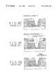
- FIG. 1is a schematic plan view showing a channel-etched type TFT which is formed on an active matrix substrate of a conventional liquid crystal display device, in which the layout of a pixel is a shown.
- FIG. 2is a cross sectional view of the TFT of FIG. 1 .
- FIGS. 3A and 3Bare cross sectional views of pads of the TFT of FIGS. 1 and 2, in which FIG. 3A shows a gate pad section and FIG. 3B shows a data pad section.
- a gate electrode 2 ais formed on a transparent insulator substrate 1 , and a gate insulator layer 3 is deposited so as to cover the transparent insulator substrate 1 and the gate electrode 2 a .
- a semiconductor layer 4is formed so as to overlay on the gate electrode 2 a .
- a source electrode 6 a and a drain electrode 7which are formed on different sides of the semiconductor layer 4 , are respectively connected to the semiconductor layer 4 via an ohmic contact layer 5 .
- Part of the deposited ohmic contact layer 5 between the source electrode 6 a and the drain electrode 7is removed by etching, and thus the ohmic contact layer 5 remains only between the source electrode 6 a and the semiconductor layer 4 and between the drain electrode 7 and the semiconductor layer 4 .
- a passivation layer 8is formed.
- a transparent conductive layer for becoming a pixel electrode 9is deposited so as to be connected to the drain electrode 7 via a contact hole 11 through the passivation layer 8 .
- a scanning signalis supplied to the gate electrode 2 a via a gate line 2 b , and a video signal is supplied to the source electrode 6 a via a source line 6 b , and thereby electric charges are written in the pixel electrode 9 .
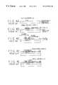
- FIGS. 4A through 4Ea manufacturing method of the active matrix substrate which has been shown in FIGS. 1 through 3B will be described referring to FIGS. 4A through 4E.
- FIGS. 4A through 4Eonly the part shown in FIG. 2 is shown in FIGS. 4A through 4E (and thus the gate pad section and the data pad section of FIGS. 3A and 3B are not shown).
- the following explanationwill be given mainly with regard to one pixel.
- a conductive layer of Al, Mo, Cr, etc.is deposited on the transparent insulator substrate 1 (formed of glass, for example) by sputtering to the thickness of 100 ⁇ 400 nm, and thereafter the first patterning step is executed so as to form the gate line 2 b (unshown in FIG. 4A, shown in FIG. 1 ), the gate electrode 2 a and a gate pad 2 c (unshown in FIG. 4A, shown in FIG. 3A) (which is connected to an external display signal processor board) are formed by photo-lithography.
- the gate insulator layer 3formed of silicon nitride
- the semiconductor layer 4formed of amorphous silicon
- the ohmic contact layer 5formed of n + amorphous silicon
- a layer of Mo, Cr, etc.is sputtered to the thickness of 100 ⁇ 200 nm so as to cover the gate insulator layer 3 and the ohmic contact layer 5 , and thereafter the third patterning step is executed so as to pattern and form the source electrode 6 a , the source line 6 b , the drain electrode 7 and a data pad 7 a (unshown in FIG. 4C, shown in FIG. 3B) (which is connected to the external display signal processor board) are formed by photo-lithography. Thereafter, unnecessary part of the ohmic contact layer 5 on the channel of the TFT is removed.
- the passivation layer 8(formed of an inorganic material such as silicon nitride) is deposited on the back channel of the TFT, the source electrode 6 a , the source line 6 b , the drain electrode 7 and the data pad 7 a (unshown in FIG. 4D, shown in FIG. 3B) by means of plasma CVD to the thickness of approximately 100 ⁇ 200 nm, and thereafter the fourth patterning step is executed so as to form the contact hole 11 (for the connection of the drain electrode 7 and the pixel if electrode 9 ) and remove unnecessary part of the passivation layer 8 on the data pad 7 a (unshown in FIG. 4D, shown in FIG. 3B) and remove unnecessary parts of the gate insulator layer 3 and the passivation layer 8 on the gate pad 2 c (unshown in FIG. 4D, shown in FIG. 3 A).
- the contact hole 11for the connection of the drain electrode 7 and the pixel if electrode 9
- the transparent conductive layer for becoming the pixel electrode 9is deposited by sputtering so as to be connected to the drain electrode 7 via the contact hole 11 through the passivation layer 8 , and thereafter the fifth patterning step is executed so as to pattern and form the pixel electrode 9 .
- a liquid crystal display deviceis manufactured by coupling the substrate and another substrate (which is provided with color filters and electrodes thereon) together so as to sandwich liquid crystal.
- the light leakagehas to be shielded by providing a black matrix (or black matrixes) to the color filter substrate (that is, the aforementioned “another substrate”).
- a black matrixor black matrixes
- the light shielding area of the black matrixeshas to be made considerably large, thereby the opening area ratio of the liquid crystal display device is necessitated to be small, and thereby the usage efficiency of the back light of the liquid crystal display device has to be lowered.
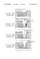
- FIGS. 5A through 5Hare cross sectional views showing the manufacturing method of the CF on TFT structure according to the above document.
- the TFT shown FIG. 5Ais called a “channel protection TFT”. Incidentally, the following explanation will be given mainly with regard to one pixel.
- a gate electrode 2 ais formed on a transparent insulator substrate 1 , and a gate insulator layer 3 is deposited so as to cover the transparent insulator substrate 1 and the gate electrode 2 a .
- a semiconductor layer 4is formed so as to overlay on the gate electrode 2 a , and a source electrode 6 a and a drain electrode 7 are formed to be connected to the semiconductor layer 4 .
- a passivation layer 8is deposited so as to cover the above structure.
- a pigments-dispersed photoresist for becoming the black matrix 15is coated on the passivation layer 8 by spin coating.
- the number of revolutions of the spin coateris controlled so that the thickness of the black matrix 15 will become approximately 1.5 ⁇ m.
- the black matrix 15is patterned by means of photo-lithography so as to overlay on the gate line 2 b . By the patterning, the black matrix 15 is formed over the channel protection TFT 10 b , and over a contact hole 11 (which will be formed later).
- a red color photoresist(pigments-dispersed type) is coated on the black matrix 15 and the passivation layer 8 by spin coating to the thickness of approximately 1.2 ⁇ m, and thereafter a red color filter 13 a is patterned to a predetermined pattern by means of photo-lithography.
- black matrixes 15The plural “black matrixes” means black matrixes corresponding to all the pixels of the liquid crystal display device.
- black matrixes 15a dim residue of the red color photoresist (pigments) tends to occur on part of the passivation layer 8 where the black matrix photoresist has been removed, or a residue of the red color photoresist tends to occur due to change of the status of the surface of the passivation layer 8 by the formation and patterning of the black matrixes 15 .
- a step for removing and cleaning a residue of the black matrix photoresisthas to be executed before the coating of the red color photoresist.
- the TFT substrate on which the black matrixes 15 have been formed and patternedis radiated with UV rays (of the luminous intensity of approximately 20 mW) for 60 sec, and the residue of the black matrix photoresist which has been broken down by the UV rays is removed by spin cleaning.
- a green color photoresist(pigments-dispersed type) is coated by spin coating to the thickness of approximately 1.2 ⁇ m, and thereafter a green color filter 13 b is patterned to a predetermined pattern by means of photo-lithography.
- a residue-removing step(for removing a residue of the red color photoresist) by use of the UV rays is necessary before the formation of the green color filter 13 b.
- a blue color photoresist(pigments-dispersed type) is coated by spin coating to the thickness of approximately 1.2 ⁇ m, and thereafter a blue color filter 13 c is patterned to a predetermined pattern by means of photo-lithography.
- a residue-removing stepfor removing a residue of the green color photoresist by use of the UV rays is necessary before the formation of the blue color filter 13 c.
- an overcoat layer 14is formed on the TFT substrate (on which the black matrixes 15 , the red color filters 13 a , the green color filters 13 b and the blue color filters 13 c have been formed) to the thickness of approximately 3 ⁇ m for flattening the surface of the TFT substrate.
- an acrylic photoresistis used as the overcoat layer 14 . After coating the overcoat layer 14 by spin coating, part of the overcoat layer 14 corresponding to the contact hole 11 is removed and opened by means of photo-lithography.
- a positive novolac photoresist 17is coated and patterned on the overcoat layer 14 , and thereafter part of the black matrix 15 corresponding to the contact hole 11 is removed and opened by means of dry etching using the novolac photoresist 17 as a mask.
- part of the passivation layer 8 corresponding to the contact hole 11is removed and opened by means of dry etching, and thereby the opening for the contact hole 11 is completed.
- a transparent conductive layer for becoming a pixel electrode 9is sputtered on the above structure, and the pixel electrode 9 is patterned to a predetermined pattern by means of photo-lithography, thereby connection between the pixel electrode 9 and the drain electrode 7 is established, and thereby the active matrix substrate of the CF (Color Filter) on TFT structure is completed.
- CFColor Filter
- the present inventorsexamined the above manufacturing method of the CF on TFT structure, some problems were found in addition to the problem which has been mentioned referring to FIG. 5 C.
- the etching of the black matrix 15 and the passivation layer 8 after hardeninghas to be done by means of dry etching.
- the black matrix 15has been formed with the thickness of approximately 1.5 ⁇ m so as to have enough light shielding effect.
- fluoride etching gasSF 6 , CF 4 , CHF 3 , etc.
- etching time of approximately 100 ⁇ 150 secis necessary for etching the passivation layer 8 which is formed of silicon nitride etc. Therefore, an etching time of approximately 300 ⁇ 450 sec is necessary for forming the contact hole opening through the black matrix 15 and the passivation layer 8 by means of dry etching even when the two dry etching steps are executed at once. Therefore, the above manufacturing method of the CF on TFT structure is not suitable for mass production.
- the generally used novolac photoresist 17does not have enough resistance to such a long etching time. Especially, if the etching of the black matrix 15 is not executed completely, some of the passivation layer 8 might remain in the contact hole 11 since the etching condition of the passivation layer 8 differs from that of the black matrix 15 , thereby contact resistance of the contact hole 11 might be increased.
- a channel protection TFT 10 bis formed on a transparent insulator substrate 1 , and a passivation layer 8 is deposited so as to cover the above structure.
- a pigments-dispersed photoresist(for becoming the black matrixes 15 ) is coated on the passivation layer 8 by spin coating.
- the number of revolutions of the spin coateris controlled so that the thickness of the black matrix 15 will become approximately 1.5 ⁇ m.
- the black matrix 15is patterned by means of photo-lithography so as to overlay on the gate line 2 b . By the patterning, the black matrix 15 is formed over the channel protection TFT 10 b , however, not formed over a contact hole 11 (which will be formed later).
- a red color photoresist(pigments-dispersed type) is coated on the black matrix 15 and the passivation layer 8 by spin coating to the thickness of approximately 1.2 ⁇ m, and thereafter a red color filter 13 a is patterned to a predetermined pattern by means of photo-lithography.
- the TFT substrate on which the black matrixes 15 have been formed and patternedis radiated with UV rays (of the luminous intensity of approximately 20 mW) for 60 sec, and the residue of the black matrix photoresist which has been broken down by the UV rays is removed by spin cleaning.
- a green color photoresist(pigments-dispersed type) is coated by spin coating to the thickness of approximately 1.2 ⁇ m, and thereafter a green color filter 13 b is patterned to a predetermined pattern by means of photo-lithography.
- a residue-removing step(for removing a residue of the red color photoresist) by use of the UV rays is necessary before the formation of the green color filter 13 b .
- a blue color filter 13 cis also formed and patterned to a predetermined pattern in a similar manner.
- an overcoat layer 14is formed on the TFT substrate (on which the black matrixes 15 , the red color filters 13 a , the green color filters 13 b and the blue color filters 13 c have been formed) to the thickness of approximately 3 ⁇ m for flattening the surface of the TFT substrate.
- an acrylic photoresistis used as the overcoat layer 14 . After coating the overcoat layer 14 by spin coating, part of the overcoat layer 14 corresponding to the contact hole 11 is removed and opened by means of photo-lithography.
- a positive novolac photoresist 17is coated and patterned on the overcoat layer 14 , and thereafter part of the passivation layer 8 corresponding to the contact hole 11 is removed and opened by means of dry etching using the novolac photoresist 17 as a mask.
- a transparent conductive layer for becoming a pixel electrode 9is sputtered on the above structure, and the pixel electrode 9 is patterned to a predetermined pattern by means of photo-lithography, thereby connection between the pixel electrode 9 and the drain electrode 7 is established, and thereby the active matrix substrate of the CF on TFT structure is completed.
- the parts of the black matrixes 15 corresponding to the contact holes 11are removed when the black matrixes 15 are developed and patterned by means of photo-lithography as shown in FIG. 6 B. Therefore, some residue of the black matrix photoresist remains on the parts of the passivation layer 8 corresponding to the contact holes 11 .
- the residue of the black matrix photoresistcan be removed to some extent by radiation of UV rays, however, in the subsequent formation steps of the red color filters 13 a , the green color filters 13 b and the blue color filters 13 c , residues of the red, green and blue color photoresists occur, growing from the faint residue of the black matrix photoresist, thereby the etching of the parts of the passivation layer 8 corresponding to the contact holes 11 is made impossible.
- the signal delayoccurs when the specific resistance of the black matrix 15 is decreased to approximately 10 6 ⁇ cm.
- the black matrix photoresistis a negative photoresist which is composed of base resin (such as acrylic acid resin) and carbon dispersed in the base resin.
- the high OD black matrix photoresistscarcely passes light, and thus photo-polymerization of the photoresist in exposure process occurs mainly on the surface only even if the amount of exposure is increased, therefore, side walls of the black matrixes 15 tend to be dissolved by the developing solution in the development process. Therefore, the tolerances of the developing time and the developing solution concentration are necessitated to be small, thereby the result of the development process tends to vary.
- the black matrixes 15can not be patterned exactly to a predetermined pattern if the development is not enough. On the other hand, parts of the black matrixes 15 flake (strip) off from the surface of the passivation layer 8 if the development is executed excessively.
- the steps for forming the parts of the CF on TFT structureare generally executed in the order: the TFTs, the black matrixes, the color filters, the overcoat layer, the contact holes, and the pixel electrodes.
- the residues of the black matrix photoresist and the color filter photoresiststend to remain in the contact hole 11 . Due to the residues, the etching of the passivation layer 8 for forming the openings for the contact holes 11 becomes impossible, and even if the contact hole 11 could successively formed, the resistance of the contact hole 11 is necessitated to become large.
- CFColor Filter
- Another object of the present inventionis to provide a manufacturing method of a liquid crystal display device, by which the liquid crystal display device having the above characteristics can be manufactured efficiently.
- a liquid crystal display devicecomprising a transparent insulator substrate, switching elements, a passivation layer, color filters of prescribed colors, black matrixes, an overcoat layer, pixel electrodes, lead electrodes, and contact holes.
- the switching elementsare formed on the transparent insulator substrate.
- the passivation layeris formed for passivating the switching elements.
- the color filters of prescribed colorsare formed on the passivation layer so that no color filter will be formed in areas around contact holes.
- the black matrixesare formed as shields for preventing light leakage.
- the black matrixesare formed on the passivation layer after the formation of the color filters so as to cover at least the switching elements, and so that no black matrix will be formed in areas around the contact holes.
- the overcoat layeris formed on the color filters and the black matrixes.
- the pixel electrodesare formed on the overcoat layer.
- the lead electrodeis provided to each of the switching elements for being connected to a corresponding one of the pixel electrodes.
- the contact holesare formed through the overcoat layer and the passivation layer for establishing connection between the pixel electrodes and lead electrodes of the switching elements.
- the black matrixesare formed so that the edge of the black matrix touching the edge of the color filter will be superposed on the edge of the color filter.
- the color filtersare formed of pigments-dispersed photoresists.
- the pigments-dispersed photoresists which are used for forming the color filtersare acrylic pigments-dispersed photoresists.
- the black matrixesare formed of a pigments-dispersed photoresist.
- the pigments-dispersed photoresist which is used for forming the black matrixesis an acrylic pigments-dispersed photoresist.
- carbon particlesare employed as the pigments for the pigments-dispersed photoresist for the black matrixes.
- carbon particles provided with insulation coatingsare employed as the pigments for the pigments-dispersed photoresist for the black matrixes.
- titanium oxide particlesare employed as the pigments for the pigments-dispersed photoresist for the black matrixes.
- the overcoat layeris formed of a transparent photoresist.
- the transparent photoresistis a transparent acrylic photoresist.
- the switching elementis a TFT (Thin-Film Transistor), and the lead electrode is the drain electrode of the TFT.
- the black matrixesare formed so as to be connected to each other across pixels which are arranged in a particular direction.
- a manufacturing method of a liquid crystal display devicecomprising a switching element formation step, a passivation layer formation step, a color filter formation step, a black matrix formation step, an overcoat layer formation step, a contact hole opening formation step, and a pixel electrode formation step.
- switching element formation stepswitching elements, each of which has a lead electrode for being connected to a corresponding pixel electrode, are formed on a transparent insulator substrate.
- passivation layer formation stepa passivation layer for passivating the switching elements is formed on the substrate on which the switching elements have been formed.
- color filters of prescribed colorsare formed on the passivation layer to predetermined patterns so that no color filter will be formed in areas around contact holes.
- black matrixesas shields for preventing light leakage, are formed on the substrate on which the color filters have been formed. The black matrixes are formed so as to cover at least the switching elements, and so that no black matrix will be formed in areas around the contact holes.
- overcoat layer formation stepan overcoat layer is formed on the substrate on which the color filters and the black matrixes have been formed. The overcoat layer is formed to a pattern having openings for the contact holes.
- the contact hole opening formation stepopenings for the contact holes are formed in the passivation layer by etching corresponding parts of the passivation layer.
- the pixel electrode formation stepthe pixel electrodes are formed on the overcoat layer by depositing a transparent conductive layer on the patterned overcoat layer and on parts of the lead electrodes which have been exposed in the contact hole openings and thereafter patterning the transparent conductive layer to a predetermined pattern.
- the black matrixesare formed so that the edge of the black matrix touching the edge of the color filter will be superposed on the edge of the color filter.
- the etching of the passivation layeris executed using a photoresist patterned on the overcoat layer as a mask.
- the etching of the passivation layeris executed using the patterned and hardened overcoat layer as a mask.
- the etching of the passivation layeris executed by means of plasma etching using one or more selected from SF 6 , He and O 2 as etching gasses.
- the color filter formation step for each prescribed colorincludes a photoresist coating step, a prebaking step, an exposure step, a development step, and a baking step.
- the color filtersare formed of pigments-dispersed photoresists.
- the pigments-dispersed photoresists which are used for forming the color filtersare acrylic pigments-dispersed photoresists.
- the black matrix formation stepincludes a photoresist coating step, a prebaking step, an exposure step, a development step, and a baking step.
- the exposure stepis executed in a nitrogen gas atmosphere.
- the black matrix formation stepincludes a photoresist coating step, a prebaking step, an exposure step, a PEB (Post Exposure Bake) step, a development step, and a baking step.
- the exposure stepis executed in a nitrogen gas atmosphere.
- the black matrix formation stepincludes a photoresist coating step, a first prebaking step, an oxygen passivation layer coating step, a second prebaking step, an exposure step, a PEB (Post Exposure Bake) step, an oxygen passivation layer removing step, a development step, and a baking step.
- the exposure stepis executed in a nitrogen gas atmosphere.
- the oxygen passivation layeris formed of polyvinyl alcohol resin.
- the black matrixesare formed of a pigments-dispersed photoresist.
- the pigments-dispersed photoresist which is used for forming the black matrixesis an acrylic pigments-dispersed photoresist.
- carbon particlesare employed as the pigments for the pigments-dispersed photoresist for the black matrixes.
- carbon particles provided with insulation coatingsare employed as the pigments for the pigments-dispersed photoresist for the black matrixes.
- titanium oxide particlesare employed as the pigments for the pigments-dispersed photoresist for the black matrixes.
- an initialization agent having high sensitivity for the “g”, “h” and “i” linesis added to the pigments-dispersed photoresist for the black matrixes.
- the black matrixesare formed so as to be connected to each other across pixels which are arranged in a particular direction.
- the manufacturing methodfurther comprises an HMDS (HexaMethylDiSilane) exposure step in which the substrate is exposed to an HMDS gas atmosphere before the color filter formation step.
- HMDSHexaMethylDiSilane
- the manufacturing methodfurther comprises an HMDS (HexaMethylDiSilane) exposure step in which the substrate is exposed to an HMDS gas atmosphere before the black matrix formation step.
- HMDSHexaMethylDiSilane
- the overcoat layeris formed of a transparent photoresist.
- the transparent photoresistis a transparent acrylic photoresist.
- the switching element which is formed in the switching element formation stepis a TFT (Thin-Film Transistor), and the lead electrode is the drain electrode of the TFT.
- TFTThin-Film Transistor
- FIG. 1is a schematic plan view showing a channel-etched type TFT which is formed on an active matrix substrate of a conventional liquid crystal display device;
- FIG. 2is a cross sectional view of the TFT of FIG. 1;
- FIGS. 3A and 3Bare cross sectional views of pads of the TFT of FIGS. 1 and 2, in which FIG. 3A shows a gate pad section and FIG. 3B shows a data pad section;
- FIGS. 4A through 12Hare cross sectional views showing a conventional manufacturing method of an active matrix substrate of FIGS. 1 through 3B;
- FIGS. 5A through 5Hare cross sectional views showing a conventional manufacturing method of a liquid crystal display device of CF on TFT structure
- FIGS. 6A through 6Gare cross sectional views showing another conventional manufacturing method of a liquid crystal display device of CF on TFT structure
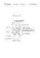
- FIG. 7is a circuit diagram for explaining the composition of a liquid crystal display device
- FIGS. 8A and 8Bare schematic plan views showing the layout of a pixel of the liquid crystal display device of FIG. 7;
- FIG. 9is a cross sectional view of the pixel layout of FIGS. 8A and 8B taken along the line A-A′ shown in FIG. 8A;
- FIG. 10is a schematic plan view showing another example of the pixel layout of the liquid crystal display device of FIG. 7;
- FIG. 11is a cross sectional view of the pixel layout of FIG. 10;
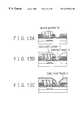
- FIGS. 12A through 12Hare cross sectional views showing a manufacturing method of the liquid crystal display device of FIG. 9 according to the first embodiment of the present invention.
- FIGS. 13A through 13Care cross sectional views showing the latter half of a manufacturing method of the liquid crystal display device of FIG. 9 according to the second embodiment of the present invention.
- FIGS. 14A through 14Eare cross sectional views showing a black matrix formation process of a manufacturing method of a liquid crystal display device according to the third embodiment of the present invention.
- FIG. 7is a circuit diagram for explaining the composition of a liquid crystal display device.
- TFTsThin-Film Transistors
- gate lines 2 b and source lines 6 bare formed so as to intercross at right angles.
- Each TFT 10is formed corresponding to each intersection of the signal lines (the gate line 2 b and the source line 6 b ).
- the gate line 2 bis connected to the gate electrode of the TFT 10 , and the TFT 10 corresponding to a pixel is driven by a scanning signal which is supplied to its gate electrode via the gate line 2 b .
- the source line 6 bis connected to the source electrode of the TFT 10 , and a video signal is supplied to the source electrode via the source line 6 b .
- the drain electrode of the TFT 10is connected to a corresponding pixel electrode 9 .
- a pixel capacitance 16is formed by a liquid crystal layer 18 which is sandwiched between the pixel electrode 9 and a common electrode on the opposite substrate.
- the pixel electrode 9overlays on the adjacent gate line 2 b (as shown in FIG. 8A) via a gate insulator layer, and thereby the pixel electrode 9 also forms an additional storage capacitance.
- FIGS. 8A and 8Bare schematic plan views showing the layout of a pixel of the liquid crystal display device of FIG. 7 .
- FIG. 8Ashows the relationship between electrodes, lines. etc.
- FIG. 8Bshows the relationship between the pixel electrode 9 , a color filter 13 and the black matrix 15 .
- Beneath each pixel electrode 9a corresponding color filter 13 is formed.
- an overcoat layer 14is formed between the color filters 13 and the pixel electrodes 9 .
- a passivation layer 8(unshown in FIGS.
- the pixel electrode 9is formed to overlay on the source lines 6 b so as to prevent the light leakage between the pixel electrode 9 and the source line 6 b . In such cases, the black matrixes 15 do not need to cover the source line 6 b , and thus the black matrixes 15 are formed so as to cover the gate lines 2 b .
- a contact hole 11is formed through an opening of the passivation layer 8 and the overcoat layer 14 , for connecting the drain electrode 7 of the TFT and the pixel electrode 9 .
- the black matrix 15is not formed around the contact hole 11 .
- the gate lines 2 b and the source lines 6 bare formed so as to intercross at right angles.
- a TFT(a source electrode 6 a , a gate electrode 2 a and a drain electrode 7 ) is formed.
- the gate line 2 b and the source line 6 bare connected to the gate electrode 2 a and the source electrode 6 a of the TFT, respectively.
- a corresponding pixel electrode 9is connected to the drain electrode 7 of the TFT via the contact hole 11 through the overcoat layer 14 and the passivation layer 8 .
- a scanning signalis supplied to the gate electrode 2 a via the gate line 2 b , and a video signal is supplied to the source electrode 6 a via the source line 6 b , and thereby electric charges are written in the pixel electrode 9 .
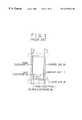
- FIG. 9is a cross sectional view of the pixel layout of FIGS. 8A and 8B taken along the line A-A′ shown in FIG. 8 A.
- FIG. 9represents the characteristics of the present invention best.
- a gate electrode 2 ais formed on a transparent insulator substrate 1 , and a gate insulator layer 3 is deposited so as to cover the transparent insulator substrate 1 and the gate electrode 2 a .
- a semiconductor layer 4is formed so as to overlay on the gate electrode 2 a .
- a source electrode 6 a and a drain electrode 7which are formed on different sides of the semiconductor layer 4 , are respectively connected to the semiconductor layer 4 via an ohmic contact layer 5 .
- a passivation layer 8is formed on the above structure (including the part where the ohmic contact layer has been removed.
- Such a TFTis generally called a “channel-etched TFT”.
- the drain electrode 7When the TFT is used as a switching element of a pixel of a liquid crystal display device, the drain electrode 7 operates also as a lead electrode to a corresponding pixel electrode 9 .
- the drain electrode 7is connected to the pixel electrode 9 via the contact hole 11 through the passivation layer 8 and the overcoat layer 14 .
- color filters 13(R, G and B) are formed corresponding to pixel display areas of the liquid crystal display device.
- the color filters 13are not formed around the contact holes 11 . Therefore, the color filter layer (composed of the color filters 13 ) has openings corresponding to the areas around the contact holes 11 .
- FIGS. 8A through 9it is also possible to make openings in the black matrixes 15 as shown in FIG. 10 (plan view) and FIG. 11 (cross sectional view).
- the color filter 13is placed behind the opening (the area around the contact hole 11 ) in FIG. 11, and thus the color filter 13 is not shown in FIG. 11 .
- the black matrixes 15are formed on the passivation layer 8 as a shade so as to cover the gate lines 2 b and the TFTs, for preventing the light leakage and for protecting the TFTs from light.
- the black matrix patternis determined based on the relationship between the pixel electrode 9 and the source lines 6 b and the relationship between the pixel electrode 9 and the gate lines 2 b , so as to prevent the light leakage.
- the black matrixes 15are formed so as to over the TFTs at least. It is also possible to form the black matrixes 15 so as to cover all the gaps between the color filters 13 . However, in every case, the openings, where no color filter 13 nor black matrix 15 is formed, re necessarily provided around the contact holes 11 .
- the black matrix 15is formed to cover the edge of the color filter 13 (that is, the edge of the black matrix 15 is superposed on the edge of the color filter 13 ) as shown in FIG. 9 .
- the relationship between the color filter 13 and the black matrix 15also holds in the example of FIG. 11 although not shown.
- the side wall of the black matrix 15(at least part near the passivation layer 8 ) is protected by the color filter 13 and is not exposed to the developing solution in the development process, thereby the pattern flake-off of the black matrixes 15 (which has been mentioned as a problem of the prior art) can be reduced.
- the black matrixes 15are formed so as to be connected to each other across pixels arranged in the horizontal direction (i.e. the direction of the gate line 2 b ). By such formation, the pattern flake-off of the black matrixes 15 can be reduced further.
- the structure mentioned aboveis implemented by forming the black matrixes 15 after the formation of the color filters 13 .
- the black matrixes 15are formed after the formation of the color filters 13 , and in the formation of the color filters 13 and the black matrixes 15 , the areas around the contact holes 11 are reserved as the openings for the contact holes 11 .
- an opening for the contact hole 11 to reach the drain electrode 7 through the passivation layer 8can be formed by etching the passivation layer 8 easily and reliably.
- the color filters 13are formed before the formation of the black matrixes 15 . According to experiments conducted by the present inventors, it became clear that no residues of the color filters 13 remain in the contact hole openings around which no color filter 13 nor black matrix 15 is formed.
- the residue problem described aboveoccurs commonly when pigments-dispersed photoresists are used for the color filters 13 and the black matrixes 15 . Therefore, the present invention is especially effective for cases where the color filters 13 and the black matrixes 15 are formed of pigments-dispersed photoresists.
- the present inventionis the most effective in the case where acrylic pigments-dispersed photoresists (which are widely used as materials of color filters) are employed.
- Pigmentscan be selected arbitrarily depending on colors.
- Carbon particles having insulation coatingsare most preferably employed in the present invention as the pigments for the lack matrixes photoresist.
- color filters 13R, G and B
- organic pigments etc.can be selected and used.
- the present inventioncan be effectively applied to liquid crystal display devices as long as the connection between the pixel electrode 9 and the switching element (TFT 10 etc.) is established through the color filter layer or the black matrix layer.
- the switching elementis not particularly limited to a TFT, and an MIM (Metal-Insulator-Metal) diode, etc. can also be employed as the switching element. While the TFT shown in the figures is of inverse-staggered type in which the gate electrode is placed lower than the source electrode and the drain electrode, a TFT of staggered type can also be employed in the liquid crystal display device according to the present invention.
- the other composition than those which have been described aboveare not particularly restricted, and can be designed according to general design of liquid crystal display devices.
- the color filters 13are generally composed of red color filters 13 a , green color filters 13 b and blue color filters 13 c , however, the filter composition can be varied if necessary.
- FIGS. 12A through 12Hare cross sectional views showing a manufacturing method of the liquid crystal display device shown in FIG. 9, according to the first embodiment of the present invention. Incidentally, the following explanation will be given mainly with regard to one pixel.
- a channel-etched TFT 10 ais formed on a transparent insulator substrate 1 such as a glass substrate.
- the channel-etched TFT 10 acan be formed similarly to the conventional manufacturing method, as follows:
- a conductive layer of Al, Mo, Cr, etc.is sputtered on the transparent insulator substrate 1 to the thickness of 100 ⁇ 400 nm, and thereafter the gate line 2 b (unshown in FIG. 12A, shown in FIG. 8 A), the gate electrode 2 a and the gate pad 2 c (unshown in FIG. 12A, shown in 7 ) (which is connected to an external display signal processor board) are formed by photo-lithography.
- the gate insulator layer 3formed of silicon nitride
- the semiconductor layer 4formed of amorphous silicon
- the ohmic contact layer 5formed of n 30 amorphous silicon
- plasma CVDChemical Vapor Deposition
- a layer of Mo, Cr, etc.is sputtered to the thickness of 100 ⁇ 200 nm so as to cover the gate insulator layer 3 and the ohmic contact layer 5 , and thereafter the source electrode 6 a , the source line 6 b (unshown in FIG. 12A, shown in FIG. 8 A), the drain electrode 7 and the data pad 7 a (unshown in FIG. 12A, shown in FIG. 7) (which is connected to the external display signal processor board) are formed by photo-lithography. Thereafter, unnecessary part of the ohmic contact layer 5 on the channel of the TFT is removed.
- the passivation layer 8(formed of an inorganic material such as silicon nitride) is deposited on the back channel of the TFT, the source electrode 6 a , the source line 6 b (unshown in FIG. 12A, shown in FIG. 8 A), the drain electrode 7 and the data pad 7 a (unshown in FIG. 12A, shown in FIG. 7) by means of plasma CVD to the thickness of approximately 100 ⁇ 200 nm, thereby the channel-etched TFT 10 a shown in FIG. 12A has been formed.
- the passivation layer 8formed of an inorganic material such as silicon nitride
- a negative pigments-dispersed red color photoresist(acrylic resin in which red pigments have been dispersed) is coated on the substrate by spin coating.
- the number of revolutions of the spin coateris controlled so that the thickness of the red color photoresist will become approximately 1.2 ⁇ m.
- the substrateis prebaked (80° C., 2 min), exposed, and developed by a TMAH (TetraMethylAmmonium Hydro-oxide) solution, and thereby the red color filter 13 a is patterned into a predetermined pattern.
- TMAHTetraMethylAmmonium Hydro-oxide
- the opening 20(where the red color filter 13 a is not formed) is provided so that the contact hole 11 for connecting the drain electrode 7 and the pixel electrode 9 can be formed later.
- the diameter of the opening 20is set large enough so that the contact hole 11 can be formed therein.
- the substrateis baked (220° C., 60 min) in a clean oven and thereby the red color filter 13 a is hardened.
- a step for removing and cleaning a residue of the red color photoresistis executed.
- the substrate on which the red color filters 13 a have been formed and patternedis radiated with UV rays (of the luminous intensity of approximately 20 mW) for 60 sec, and the residue of the red color photoresist which has been broken down by the UV rays is removed by spin cleaning.
- the green color filter 13 bis formed in the same way as the red color filter 13 a .
- a step for removing and cleaning a residue of the green color photoresistis executed, similarly to the residue-removing step for the red color photoresist.
- the blue color filter 13 cis formed in the same way.
- a step for removing and cleaning a residue of the blue color photoresistis executed, similarly to the residue-removing steps for the red and green color photoresists.
- the black matrix 15is formed as shown in FIG. 12 E.
- a pigments-dispersed black matrix photoresist(acrylic resin in which black pigments such as carbon have been dispersed) is preferably used.
- the pigments-dispersed black matrix photoresist of a viscosity of 20 cpis coated on the substrate by spin coating to the thickness of approximately 1.5 ⁇ m, and thereafter the black matrix photoresist is patterned to a predetermined pattern of the black matrixes 15 so that no black matrix 15 will be formed on the contact holes 11 .
- the patterning of the black matrixes 15is executed similarly to the patterning of the color filters 13 (coating of the black matrix photoresist, prebaking, exposure, development and baking.
- a step for removing and cleaning a residue of the black matrix photoresistis executed, similarly to the residue-removing steps for the red, green and blue color photoresists.
- the black matrix photoresistis a negative photoresist which hardly passes light, therefore, radicals are generated on the surface of the black matrix photoresist by enough exposure to light.
- the radicalsdisperses inside the black matrix photoresist, thereby the photo-polymerization proceeds also in the depths (i.e. parts far from the surface) of the black matrix photoresist.
- the strength of the photo-polymerization in the depthsis weaker than on the surface. Therefore, in the present invention, the tolerance of development is gained by protecting the side walls of the black matrixes 15 by the color filters 13 .
- an initialization agent having high sensitivity for the “g”, “h” and “i” linesis preferably selected and added to the black matrix photoresist. It is also effective to execute the exposure of the black matrix photoresist to light in a nitrogen gas atmosphere, so as to prevent the radicals from being quenched by ozone which is generated by decomposition of oxygen gas in the exposure. In order to let the radicals disperse effectively in the depths of the black matrix 15 , so called “PEB (Post Exposure Bake) process can be executed.
- PEBPost Exposure Bake
- HMDSHexaMethylDiSilane
- exposing the substrate in an HMDS gas atmosphere before the coating of the black matrix photoresistcan also be employed for improving the adhesion of the black matrixes 15 to the foundations.
- a transparent acrylic photoresist(for becoming the overcoat layer 14 ) is coated on the substrate so as to flatten the surface of the substrate, and the transparent acrylic photoresist layer is patterned by exposure and development so as to have openings for the contact holes 11 .
- the patterned transparent acrylic photoresist layeris hardened by baking (220° C., 60 min), and thereby the overcoat layer 14 is formed.
- a novolac photoresist 17for example, is coated and patterned on the overcoat layer 14 , and thereafter part of the passivation layer 8 is etched using the novolac photoresist 17 as a mask, thereby openings for the contact holes 11 are formed through the passivation layer 8 .
- the opening for the contact hole 11was formed in the above explanation in two steps (formation of an opening through the overcoat layer 14 and formation of an opening through the passivation layer 8 ), it is also possible to form the contact hole opening by etching the overcoat layer 14 and the passivation layer 8 at once, that is, without the patterning of the overcoat layer 14 .
- the black matrixes 15are formed after the formation of the color filters 13 . Therefore, the residues of the color filter photoresists and the black matrix photoresist do not occur in the contact hole 11 at all, and thus no problem occurs in the subsequent etching of the passivation layer 8 . Further, the openings for the contact holes 11 are formed just before the sputtering of the transparent conductive layer for becoming the pixel electrodes 9 (that is, no other process is executed between the formation of the contact hole openings and the sputtering of the transparent conductive layer for the pixel electrodes 9 ), therefore, the openings for the contact holes 11 are not oxidized nor contaminated by process. Therefore, the resistance of the connection between the drain electrode 7 and the pixel electrode 9 is reduced, and thereby a satisfactory active matrix substrate can be obtained.
- a transparent conductive layer of ITO (Indium-Tin-Oxide) etc. for becoming the pixel electrodes 9is sputtered on the overcoat layer 14 and on the parts of the drain electrodes 7 exposed in the contact holes 11 .
- the transparent conductive layeris thereafter patterned to a predetermined pattern, thereby the pixel electrodes 9 are formed.
- the transparent conductive layeris deposited thicker, the coverage of the transparent conductive layer in the contact hole 11 becomes better and thereby electrical connection of the pixel electrode 9 to the drain electrode 7 becomes more stable.
- an appropriate thickness of the pixel electrode 9is 100 nm or so.
- the substrateis coupled with the opposite substrate and liquid crystal is poured and packed between the substrates according to an ordinary manufacturing method, thereby the liquid crystal display device is completed.
- the thicknesses of the color filter 13 and the black matrix 15are preferably set according to materials which are employed for them. When generally used materials are employed, the thicknesses of the color filter 13 and the black matrix 15 (when coated) are approximately 1.0 ⁇ 1.5 ⁇ m and 1.0 ⁇ 2.0 ⁇ m, respectively.
- the thickness of the overcoat layer 14is set to be capable of flattening the surface of the substrate, to approximately 2.5 ⁇ 4.5 ⁇ m when coated.
- the black matrixes 15are formed after the formation of the color filters 13 , thereby the residues in the opening for the contact hole 11 for connecting the switching element (TFT etc.) and the pixel electrode 9 is eliminated. Therefore, etching of the passivation layer 8 for forming the openings for the contact holes 11 can be executed easily and reliably, and the resistance of the connection between the switching element and the pixel electrode 9 is reduced, and thus a satisfactory active matrix substrate of on-array color filter structure can be obtained.
- the passivation layer 8 for forming the openings for the contact holes 11can be executed easily and reliably, and the resistance of the connection between the switching element and the pixel electrode 9 is reduced, and thus a satisfactory active matrix substrate of on-array color filter structure can be obtained.
- the black matrixes 15have not been formed at the points when the residue-removing steps for the red, green and blue color photoresists using UV rays are executed. Therefore, the deterioration of the resistance of the black matrix 15 due to excessive radiation of the UV rays is avoided, and thereby the signal delay is eliminated.
- edges of the black matrixes 15are superposed on the edges of the color filters 13 , thereby the flake-off of the side walls of the black matrixes 15 is avoided in the development process.
- FIGS. 12A through 12D and 13 A through 13 Care cross sectional views showing the latter half of a manufacturing method of the liquid crystal display device shown in FIG. 9, according to the second embodiment of the present invention.
- the first half of the manufacturing methodis executed in the same way as the first embodiment as shown in FIGS. 12A through 12D.
- the RGB color filters 13( 13 a , 13 b and 13 c ) are formed on the transparent insulator substrate 1 on which the TFTs have been completed. Incidentally, after each completion of a color filter ( 13 a , 13 b , 13 c ), a step for removing and cleaning a residue of the color photoresist is executed, as mentioned in the first embodiment.
- the black matrixes 15are formed in the same way as the first embodiment.
- a step for removing and cleaning a residue of the black matrix photoresistis executed, as mentioned in the first embodiment.
- a transparent acrylic photoresist(for becoming the overcoat layer 14 ) is coated on the TFT substrate (on which the color filters 13 a , 13 b and 13 c and the black matrixes 15 have been formed) so as to flatten the surface of the substrate, and the transparent acrylic photoresist layer is patterned by exposure and development so as to have openings for the contact holes 11 .
- the patterned transparent acrylic photoresist layeris hardened by baking (220° C., 60 min), and thereby the overcoat layer 14 is formed.
- parts of the passivation layer 8are etched using the patterned and hardened overcoat layer 14 (not the novolac photoresist 17 of the first embodiment) as a mask, thereby openings for the contact holes 11 are formed through the passivation layer 8 .
- the etching of the passivation layer 8can be conducted without using a photoresist as in the first embodiment, by selecting an etching condition by which the acrylic overcoat layer 14 is not etched.
- the PEPulsma Etching
- SF 6SF 6
- He and O 2as etching gasses
- etching conditions of the second embodimentare as follows: SF 6 flow: 60 sccm, He flow: 40 sccm, O 2 flow: 150 sccm, pressure: 40 Pa, power: 1200 W, gap (between the plasma electrode and the substrate): 50 mm, etching time: 120 sec.
- a transparent conductive layer for becoming the pixel electrodes 9is sputtered on the overcoat layer 14 and on the parts of the drain electrodes 7 exposed in the contact holes 11 .
- the transparent conductive layeris thereafter patterned to a predetermined pattern, thereby the pixel electrodes 9 are formed.
- the substrateis coupled with the opposite substrate and liquid crystal is poured and packed between the substrates according to an ordinary manufacturing method, thereby the liquid crystal display device is completed.
- the etching of the passivation layer 8 for forming the openings for the contact holes 11is conducted by dry etching using the patterned overcoat layer 14 as a mask (without using the novolac photoresist 17 ). Therefore, one photo-lithography step can be omitted in comparison with the first embodiment, thereby the manufacturing process can be shortened.
- FIGS. 14A through 14Eare cross sectional views showing a black matrix formation process of a manufacturing method of a liquid crystal display device according to the third embodiment of the present invention.
- the first half of the manufacturing methodis executed in the same way as the first and second embodiments as shown in FIGS. 12A through 12D, and thereby the RGB color filters 13 ( 13 a , 13 b and 13 c ) are formed on the transparent insulator substrate 1 on which the TFTs have been completed.
- the subsequent black matrix formation processis executed as follows:
- a negative black matrix photoresistfor becoming the black matrixes 15
- the substrateis prebaked (90° C., 2 min).
- an oxygen passivation layer 21is coated on the substrate in order to prevent the radicals (which are generated on the surface of the black matrix photoresist in exposure) from being quenched by ozone (which is generated in the atmosphere during exposure), and thereafter the substrate is prebaked again (90° C., 1 min).
- the oxygen passivation layer 21polyvinyl alcohol resin dissolved in isopropyl alcohol and water is used, for example.
- exposure of the black matrix photoresistis executed by radiating the substrate with UV rays of an energy of approximately 50 ⁇ 200 mJ (50 mW ⁇ 1 ⁇ 4 sec, for example), using a g-h-i line stepper.
- the PEB (Post Exposure Bake) process80° C., 2 min is executed in order to let the generated radicals disperse effectively into the depths of the black matrix photoresist.
- the substrateis rinsed for 1 minute and thereby the oxygen passivation layer 21 on the surfaces of the black matrix photoresist is removed.
- steps for forming the overcoat layer 14 , the contact hole 11 and the pixel electrode 9are executed in the same way as the first or second embodiment.
- the oxygen passivation layer 21is employed in the black matrix formation process, thereby the radicals which are generated in the exposure can be used effectively for the exposure and photo-polymerization of the black matrix photoresist.
- the exposurecould be reduced to ⁇ fraction (1/10) ⁇ compared to the case where the oxygen passivation layer 21 is not used, and thereby the manufacturing throughput could be raised.
- the cauliflower-like overhangs of the black matrix pattern due to the use of the oxygen passivation layer 21can be avoided, and thereby black matrixes 15 having satisfactory profiles could be obtained.
- the black matrixes 15are formed after the formation of the color filters 13 , therefore, the residues of the color filter photoresists and the black matrix photoresist remaining in the contact hole openings can be reduced or eliminated.
- the etching of the passivation layer 8 for forming the openings for the contact holes 11can be executed easily and reliably, and the contact resistance of the contact hole 11 for connecting the lead electrode of the switching element and the pixel electrode 9 can be reduced, and thus a satisfactory active matrix substrate of on-array color filter structure can be obtained.
- the black matrixes 15have not been formed at the points when the residue-removing steps for the red, green and blue color photoresists using UV rays are executed, and thus the UV cleaning process is not executed heavily on the black matrixes 15 . Therefore, the deterioration of the resistance of the black matrix 15 is avoided, thereby the increase of the coupling capacitance between the black matrix 15 and signal lines can be avoided, and thereby the signal delay can be eliminated.
- the black matrixes 15are formed so that the edge of the black matrix 15 touching the edge of the color filter 13 will be superposed on the edge of the color filter 13 . Therefore, pattern flake-off of the black matrixes 15 can be eliminated, and thus the light leakage can be eliminated correctly.
- the liquid crystal display device having the above characteristicscan be manufactured efficiently.
Landscapes
- Physics & Mathematics (AREA)
- Nonlinear Science (AREA)
- Engineering & Computer Science (AREA)
- Microelectronics & Electronic Packaging (AREA)
- Mathematical Physics (AREA)
- Chemical & Material Sciences (AREA)
- Crystallography & Structural Chemistry (AREA)
- General Physics & Mathematics (AREA)
- Optics & Photonics (AREA)
- Liquid Crystal (AREA)
- Thin Film Transistor (AREA)
- Devices For Indicating Variable Information By Combining Individual Elements (AREA)
Abstract
Description
Claims (40)
Applications Claiming Priority (4)
| Application Number | Priority Date | Filing Date | Title |
|---|---|---|---|
| JP35163798 | 1998-12-10 | ||
| JP10-351637 | 1998-12-10 | ||
| JP19774199AJP3267271B2 (en) | 1998-12-10 | 1999-07-12 | Liquid crystal display device and method of manufacturing the same |
| JP11-197741 | 1999-07-12 |
Publications (1)
| Publication Number | Publication Date |
|---|---|
| US6429916B1true US6429916B1 (en) | 2002-08-06 |
Family
ID=26510537
Family Applications (1)
| Application Number | Title | Priority Date | Filing Date |
|---|---|---|---|
| US09/459,010Expired - LifetimeUS6429916B1 (en) | 1998-12-10 | 1999-12-10 | Liquid crystal display with filter and light shield separated from contact hole |
Country Status (4)
| Country | Link |
|---|---|
| US (1) | US6429916B1 (en) |
| JP (1) | JP3267271B2 (en) |
| KR (1) | KR100376355B1 (en) |
| TW (1) | TW548500B (en) |
Cited By (70)
| Publication number | Priority date | Publication date | Assignee | Title |
|---|---|---|---|---|
| US6621544B2 (en)* | 2000-10-20 | 2003-09-16 | Sharp Kabushiki Kaisha | Liquid crystal display apparatus and projection-type liquid crystal display apparatus |
| US6657692B2 (en)* | 2000-04-19 | 2003-12-02 | Nec Corporation | Transmission liquid crystal display and method of forming the same |
| US6660646B1 (en)* | 2000-09-21 | 2003-12-09 | Northrop Grumman Corporation | Method for plasma hardening photoresist in etching of semiconductor and superconductor films |
| US20040001170A1 (en)* | 2002-06-28 | 2004-01-01 | Lg.Philips Lcd Co., Ltd. | Liquid crystal display device having array substrate of color filter on thin film transistor structure and manufacturing method thereof |
| US6674106B2 (en)* | 2000-02-29 | 2004-01-06 | Sony Corporation | Display device such as electro-optic element and thin film transistor and display device manufacturing method |
| US6693697B2 (en)* | 2001-01-11 | 2004-02-17 | Nec Lcd Technologies, Ltd. | Active-matrix type liquid crystal display device having thick and thin overcoat layers layered over a black matrix |
| US20040109110A1 (en)* | 2002-12-10 | 2004-06-10 | Lg.Philips Lcd Co., Ltd. | Array substrate of liquid crystal display device having thin film transistor on color filter structure and method of fabricating the same |
| US20040109106A1 (en)* | 2002-12-09 | 2004-06-10 | Kie-Hsiung Yang | Liquid crystal display device |
| GB2396242A (en)* | 2002-12-09 | 2004-06-16 | Lg Philips Lcd Co Ltd | Liquid crystal display with colour filter on thin film transistor structure |
| US20040125293A1 (en)* | 2002-10-14 | 2004-07-01 | Jia-Shyong Cheng | Integrated color filter and fabricating method thereof |
| US20040195571A1 (en)* | 2003-02-10 | 2004-10-07 | Lg.Philips Lcd Co., Ltd. | Method of patterning transparent conductive film, thin film transistor substrate using the same and fabricating method thereof |
| US20040202945A1 (en)* | 2000-10-20 | 2004-10-14 | Kimikazu Matsumoto | Manufacturing method of color filter substrate, active matrix type liquid crystal display, and manufacturing method of active matrix type liquid crystal display |
| US20040245523A1 (en)* | 2003-06-05 | 2004-12-09 | Tean-Sen Jen | Circular thin film transistor structure |
| US20040263065A1 (en)* | 2003-06-26 | 2004-12-30 | Industrial Technology Research Institute | Active organic light emitting diode display structure |
| US6870587B2 (en)* | 2000-05-18 | 2005-03-22 | Nec Lcd Technologies, Ltd. | Liquid crystal display device having a black matrix with a specific resistance |
| US20050122442A1 (en)* | 2003-12-03 | 2005-06-09 | Lg. Philips Lcd Co., Ltd. | Liquid crystal display device and method of fabricating the same |
| US20050139922A1 (en)* | 2003-12-27 | 2005-06-30 | Lg.Philips Lcd Co., Ltd. | Liquid crystal display device and manufacturing method thereof |
| US20050140915A1 (en)* | 2003-12-27 | 2005-06-30 | Seung-Han Paek | Liquid crystal display device having column spacers and method of fabricating the same |
| US20050233259A1 (en)* | 2004-04-02 | 2005-10-20 | Matsushita Electric Industrial Co., Ltd. | Resist material and pattern formation method using the same |
| US20050243231A1 (en)* | 2004-04-30 | 2005-11-03 | Masahiro Horiguchi | Liquid crystal device and electronic apparatus |
| US20050253917A1 (en)* | 2004-05-13 | 2005-11-17 | Quanyuan Shang | Method for forming color filters in flat panel displays by inkjetting |
| US7016009B2 (en)* | 2000-08-26 | 2006-03-21 | Lg.Philips Lcd Co., Ltd. | Method for manufacturing liquid crystal display device with particular pad protection layers |
| US20060092199A1 (en)* | 2004-11-04 | 2006-05-04 | White John M | Methods and apparatus for aligning print heads |
| US20060092207A1 (en)* | 2004-11-04 | 2006-05-04 | Bassam Shamoun | Methods and apparatus for precision control of print head assemblies |
| US20060093751A1 (en)* | 2004-11-04 | 2006-05-04 | Applied Materials, Inc. | System and methods for inkjet printing for flat panel displays |
| US20060092218A1 (en)* | 2004-11-04 | 2006-05-04 | Applied Materials, Inc. | Methods and apparatus for inkjet printing |
| US20060099526A1 (en)* | 2004-11-10 | 2006-05-11 | Nam-Choul Yang | Organic thin film transistor, method of manufacturing the same, and flat panel display having the same |
| US20060134939A1 (en)* | 2004-03-01 | 2006-06-22 | Anritsu Company | Method for forming hermetic glass bead assembly having high frequency compensation |
| US20060139516A1 (en)* | 2004-12-28 | 2006-06-29 | Seung-Ryull Park | Liquid crystal display device and black matrix for liquid crystal display device |
| US20060290829A1 (en)* | 2003-03-28 | 2006-12-28 | Dong-Gyu Kim | Liquid crystal display and thin film transistor array panel therefor |
| US20070015848A1 (en)* | 2005-07-15 | 2007-01-18 | Lizhong Sun | Green printing ink for color filter applications |
| US20070023837A1 (en)* | 2005-07-27 | 2007-02-01 | Samsung Electronics Co., Ltd. | Thin film transistor substrate and method of making the same |
| US20070035676A1 (en)* | 2005-08-12 | 2007-02-15 | Semiconductor Energy Laboratory Co., Ltd. | Liquid crystal display device and method for manufacturing the same |
| US20070065571A1 (en)* | 2005-09-19 | 2007-03-22 | Applied Materials. Inc. | Method and apparatus for manufacturing a pixel matrix of a color filter for a flat panel display |
| US20070164286A1 (en)* | 2003-04-04 | 2007-07-19 | Dong-Gyu Kim | Liquid crystal display, thin film transistor array panel therefor, and manufacturing method thereof |
| US20080002112A1 (en)* | 2006-06-29 | 2008-01-03 | Byung-Joo Lee | Liquid crystal display device and fabrication method thereof |
| CN100365491C (en)* | 2002-09-09 | 2008-01-30 | 三星电子株式会社 | Multi-domain liquid crystal display and its thin film transistor substrate |
| US20080043164A1 (en)* | 2002-12-09 | 2008-02-21 | Youn-Gyoung Chang | Array substrate having color filter on the film transistor structure for LCD device and method of fabricating the same |
| CN100419552C (en)* | 2003-12-10 | 2008-09-17 | 三星电子股份有限公司 | Thin Film Transistor Array Panel |
| CN100422831C (en)* | 2004-12-31 | 2008-10-01 | 乐金显示有限公司 | Liquid crystal display device and manufacturing method thereof |
| US20090108256A1 (en)* | 2007-10-31 | 2009-04-30 | Sang-Ki Kwak | Thin-film transistor substrate and method of manufacturing the same |
| US20090141218A1 (en)* | 2007-10-26 | 2009-06-04 | Applied Materials, Inc. | Methods and apparatus for curing pixel matrix filter materials |
| US7544723B2 (en) | 2005-07-15 | 2009-06-09 | Applied Materials, Inc. | Blue printing ink for color filter applications |
| US20090167974A1 (en)* | 2007-12-26 | 2009-07-02 | Samsung Electronics Co., Ltd. | Display substrate, display device including the display substrate and method of fabricating the display substrate |
| US7611217B2 (en) | 2005-09-29 | 2009-11-03 | Applied Materials, Inc. | Methods and systems for inkjet drop positioning |
| US20090273752A1 (en)* | 2001-03-29 | 2009-11-05 | Nec Lcd Technologies, Ltd. | Liquid crystal display having transparent conductive film on interlayer insulating film formed by coating |
| US7637587B2 (en) | 2007-08-29 | 2009-12-29 | Applied Materials, Inc. | System and method for reliability testing and troubleshooting inkjet printers |
| US20100210052A1 (en)* | 2005-05-06 | 2010-08-19 | Jang-Soo Kim | Thin film transistor panel, liquid crystal display having the same and method of manufacturing the thin film transistor panel |
| US7857413B2 (en) | 2007-03-01 | 2010-12-28 | Applied Materials, Inc. | Systems and methods for controlling and testing jetting stability in inkjet print heads |
| US7923057B2 (en) | 2006-02-07 | 2011-04-12 | Applied Materials, Inc. | Methods and apparatus for reducing irregularities in color filters |
| US20120112346A1 (en)* | 2010-11-04 | 2012-05-10 | Ning Hong Long | Thin-film transistor substrate and method of manufacturing the same |
| CN102629578A (en)* | 2011-09-29 | 2012-08-08 | 京东方科技集团股份有限公司 | TFT array substrate and manufacturing method thereof and display device |
| US20130155354A1 (en)* | 2011-12-19 | 2013-06-20 | Shenzhen China Star Optoelectronics Technology Co., Ltd. | Liquid crystal display device and manufacture method thereof |
| US20130250220A1 (en)* | 2012-03-23 | 2013-09-26 | Samsung Display Co., Ltd. | Liquid crystal display and manufacturing method thereof |
| US20140183535A1 (en)* | 2012-12-27 | 2014-07-03 | Samsung Display Co., Ltd. | Thin film transistor array panel and method of manufacturing the same |
| CN103956335A (en)* | 2014-03-17 | 2014-07-30 | 京东方科技集团股份有限公司 | Preparation method of array substrate |
| US8890187B2 (en) | 2010-04-16 | 2014-11-18 | Semiconductor Energy Laboratory Co., Ltd. | Light-emitting device with an insulating partition |
| US20150103282A1 (en)* | 2013-10-14 | 2015-04-16 | Samsung Display Co., Ltd. | Liquid crystal display and manufacturing method thereof |
| US9025112B2 (en)* | 2012-02-02 | 2015-05-05 | Apple Inc. | Display with color mixing prevention structures |
| US9035300B2 (en) | 2013-05-24 | 2015-05-19 | Samsung Display Co., Ltd. | Array substrate comprising a thin film transistor and a pixel electrode |
| US20150249120A1 (en)* | 2013-09-09 | 2015-09-03 | Boe Technology Group Co., Ltd. | Oled array substrate, manufacturing method and display device thereof |
| CN105308752A (en)* | 2013-03-29 | 2016-02-03 | 乐金显示有限公司 | Thin-film transistor, method for manufacturing the same and display device including the same |
| US9634030B2 (en)* | 2015-07-10 | 2017-04-25 | Shenzhen China Star Optoelectronics Technology Co., Ltd. | Array substrate and manufacturing method thereof |
| CN106597734A (en)* | 2017-02-22 | 2017-04-26 | 北京京东方光电科技有限公司 | Display substrate and display device |
| CN106842685A (en)* | 2017-03-16 | 2017-06-13 | 惠科股份有限公司 | Display panel, manufacturing method and display device |
| US9829740B2 (en) | 2014-07-23 | 2017-11-28 | Apple Inc. | Display with reduced color mixing |
| CN107589582A (en)* | 2017-09-04 | 2018-01-16 | 深圳市华星光电技术有限公司 | COA display panels and preparation method thereof, COA display devices |
| US10008608B2 (en) | 2008-11-28 | 2018-06-26 | Semiconductor Energy Laboratory Co., Ltd. | Liquid crystal display device |
| US10578784B2 (en)* | 2017-09-04 | 2020-03-03 | Shenzhen China Star Optoelectronics Technology Co., Ltd | Color-filter on array (COA) display panel, manufacturing method thereof and COA display device |
| US20230154932A1 (en)* | 2020-04-23 | 2023-05-18 | Shenzhen China Star Optoelectronics Semiconductor Display Technology Co., Ltd. | Array substrate and fabrication method thereof, and display device |
Families Citing this family (24)
| Publication number | Priority date | Publication date | Assignee | Title |
|---|---|---|---|---|
| KR100749459B1 (en)* | 2000-11-14 | 2007-08-14 | 삼성에스디아이 주식회사 | LCD with color filter formed on TF array and its manufacturing method |
| KR100746140B1 (en)* | 2000-12-28 | 2007-08-03 | 엘지.필립스 엘시디 주식회사 | Array substrate for liquid crystal display device and manufacturing method thereof |
| JP4689851B2 (en)* | 2001-02-23 | 2011-05-25 | Nec液晶テクノロジー株式会社 | Active matrix liquid crystal display device |
| JP2002296618A (en)* | 2001-03-29 | 2002-10-09 | Nec Corp | Liquid crystal display device and its manufacturing method |
| JP2003005168A (en) | 2001-06-18 | 2003-01-08 | Nec Corp | Manufacturing method for liquid crystal display device |
| JP4876341B2 (en) | 2001-07-13 | 2012-02-15 | 日本電気株式会社 | Active matrix substrate and manufacturing method thereof |
| JP2003172946A (en) | 2001-09-28 | 2003-06-20 | Fujitsu Display Technologies Corp | Liquid crystal display device substrate and liquid crystal display device using the same |
| US7102168B2 (en) | 2001-12-24 | 2006-09-05 | Samsung Electronics Co., Ltd. | Thin film transistor array panel for display and manufacturing method thereof |
| KR100890024B1 (en) | 2002-09-18 | 2009-03-25 | 삼성전자주식회사 | Liquid crystal display |
| KR100925458B1 (en) | 2003-01-17 | 2009-11-06 | 삼성전자주식회사 | Thin film transistor array panel and manufacturing method thereof |
| JP4278034B2 (en) | 2003-03-10 | 2009-06-10 | シャープ株式会社 | Display device substrate, manufacturing method thereof, and display device including the same |
| KR101022807B1 (en)* | 2003-12-26 | 2011-03-17 | 엘지디스플레이 주식회사 | Array Board for Reflective Liquid Crystal Display and Manufacturing Method Thereof |
| KR101122234B1 (en) | 2005-04-13 | 2012-06-12 | 삼성전자주식회사 | Color filter array panel, liquid crystal display including the same and manufacturing method thereof |
| KR100877218B1 (en)* | 2006-05-22 | 2009-01-07 | 세심광전자기술(주) | Multi-domain Vertically Aligned Liquid Crystal Display |
| KR101415563B1 (en) | 2007-12-07 | 2014-07-07 | 삼성디스플레이 주식회사 | Thin film transistor display panel and manufacturing method thereof |
| KR101682092B1 (en) | 2009-11-12 | 2016-12-05 | 삼성디스플레이 주식회사 | Thin film transistor array panel and liquid crystal display including the same |
| TWI743509B (en)* | 2011-05-05 | 2021-10-21 | 日商半導體能源研究所股份有限公司 | Semiconductor device and method for manufacturing the same |
| CN102651339B (en)* | 2011-09-29 | 2014-11-05 | 京东方科技集团股份有限公司 | TFT (Thin Film Transistor) array substrate and manufacturing method and display device of TFT array substrate |
| JP2014077925A (en)* | 2012-10-11 | 2014-05-01 | Japan Display Inc | Liquid crystal display device |
| KR20140057015A (en) | 2012-11-02 | 2014-05-12 | 삼성디스플레이 주식회사 | Nano crystal display |
| US9417475B2 (en)* | 2013-02-22 | 2016-08-16 | Semiconductor Energy Laboratory Co., Ltd. | Display device |
| CN104765216B (en)* | 2015-04-30 | 2017-12-19 | 京东方科技集团股份有限公司 | Array base palte and preparation method thereof and display device |
| CN107479286B (en)* | 2017-09-04 | 2020-08-04 | 深圳市华星光电技术有限公司 | Via hole structure for improving gray scale twill |
| CN119992978B (en)* | 2024-11-29 | 2025-09-26 | 友达光电股份有限公司 | Transparent display |
Citations (8)
| Publication number | Priority date | Publication date | Assignee | Title |
|---|---|---|---|---|
| US5172256A (en) | 1988-01-19 | 1992-12-15 | Sethofer Nicholas L | Liquid crystal variable color density lens and eye protective devices incorporating the same |
| KR950012112A (en) | 1993-10-06 | 1995-05-16 | 김광호 | Color filter for liquid crystal display (LCD) and its manufacturing method |
| JPH1039292A (en) | 1996-07-24 | 1998-02-13 | Toshiba Electron Eng Corp | Liquid crystal display device |
| US5724109A (en)* | 1992-09-17 | 1998-03-03 | Fujitsu Limited | Liquid crystal display panel with electrodes or a passivation layer intermediate two liquid crystal layers |
| US5943107A (en)* | 1994-10-19 | 1999-08-24 | Sony Corporation | Color display device |
| US6195139B1 (en)* | 1992-03-04 | 2001-02-27 | Semiconductor Energy Laboratory Co., Ltd. | Electro-optical device |
| US6198520B1 (en)* | 1995-08-03 | 2001-03-06 | Hitachi, Ltd. | Color liquid crystal display |
| US6330043B1 (en)* | 1999-04-20 | 2001-12-11 | Nec Corporation | Liquid crystal display device and method of fabrication TFT panel |
Family Cites Families (4)
| Publication number | Priority date | Publication date | Assignee | Title |
|---|---|---|---|---|
| JP3287635B2 (en)* | 1993-03-24 | 2002-06-04 | 大日本印刷株式会社 | Manufacturing method of color filter |
| KR970022431A (en)* | 1995-10-12 | 1997-05-28 | 김광호 | Color filter panel manufacturing process for thin film transistor liquid crystal display |
| JP2853656B2 (en)* | 1996-05-22 | 1999-02-03 | 日本電気株式会社 | LCD panel |
| JP3264364B2 (en)* | 1997-01-21 | 2002-03-11 | シャープ株式会社 | Manufacturing method of liquid crystal display device |
- 1999
- 1999-07-12JPJP19774199Apatent/JP3267271B2/ennot_activeExpired - Lifetime
- 1999-12-03TWTW088121147Apatent/TW548500B/ennot_activeIP Right Cessation
- 1999-12-09KRKR10-1999-0056047Apatent/KR100376355B1/ennot_activeExpired - Lifetime
- 1999-12-10USUS09/459,010patent/US6429916B1/ennot_activeExpired - Lifetime
Patent Citations (8)
| Publication number | Priority date | Publication date | Assignee | Title |
|---|---|---|---|---|
| US5172256A (en) | 1988-01-19 | 1992-12-15 | Sethofer Nicholas L | Liquid crystal variable color density lens and eye protective devices incorporating the same |
| US6195139B1 (en)* | 1992-03-04 | 2001-02-27 | Semiconductor Energy Laboratory Co., Ltd. | Electro-optical device |
| US5724109A (en)* | 1992-09-17 | 1998-03-03 | Fujitsu Limited | Liquid crystal display panel with electrodes or a passivation layer intermediate two liquid crystal layers |
| KR950012112A (en) | 1993-10-06 | 1995-05-16 | 김광호 | Color filter for liquid crystal display (LCD) and its manufacturing method |
| US5943107A (en)* | 1994-10-19 | 1999-08-24 | Sony Corporation | Color display device |
| US6198520B1 (en)* | 1995-08-03 | 2001-03-06 | Hitachi, Ltd. | Color liquid crystal display |
| JPH1039292A (en) | 1996-07-24 | 1998-02-13 | Toshiba Electron Eng Corp | Liquid crystal display device |
| US6330043B1 (en)* | 1999-04-20 | 2001-12-11 | Nec Corporation | Liquid crystal display device and method of fabrication TFT panel |
Cited By (123)
| Publication number | Priority date | Publication date | Assignee | Title |
|---|---|---|---|---|
| US6674106B2 (en)* | 2000-02-29 | 2004-01-06 | Sony Corporation | Display device such as electro-optic element and thin film transistor and display device manufacturing method |
| US20040066485A1 (en)* | 2000-04-19 | 2004-04-08 | Nec Corporation | Transmission liquid crystal display and method of forming the same |
| US6657692B2 (en)* | 2000-04-19 | 2003-12-02 | Nec Corporation | Transmission liquid crystal display and method of forming the same |
| US20060181655A1 (en)* | 2000-04-19 | 2006-08-17 | Nec Corporation | Transmission liquid crystal display and method of forming the same |
| US7057694B2 (en) | 2000-04-19 | 2006-06-06 | Nec Corporation | Transmission liquid crystal display including first transparent layer and second transparent layer made of same material |
| US7973867B2 (en) | 2000-04-19 | 2011-07-05 | Nec Corporation | Transmission liquid crystal display and method of forming the same |
| US20050134784A1 (en)* | 2000-05-18 | 2005-06-23 | Nec Lcd Technologies, Ltd | Liquid crystal display having a black matrix layer |
| US6870587B2 (en)* | 2000-05-18 | 2005-03-22 | Nec Lcd Technologies, Ltd. | Liquid crystal display device having a black matrix with a specific resistance |
| US7016009B2 (en)* | 2000-08-26 | 2006-03-21 | Lg.Philips Lcd Co., Ltd. | Method for manufacturing liquid crystal display device with particular pad protection layers |
| US6660646B1 (en)* | 2000-09-21 | 2003-12-09 | Northrop Grumman Corporation | Method for plasma hardening photoresist in etching of semiconductor and superconductor films |
| US7423709B2 (en) | 2000-10-20 | 2008-09-09 | Nec Lcd Technologies, Ltd. | Color filter substrate, manufacturing method of color filter substrate, active matrix type liquid crystal display, and manufacturing method of active matrix type liquid crystal display |
| US6621544B2 (en)* | 2000-10-20 | 2003-09-16 | Sharp Kabushiki Kaisha | Liquid crystal display apparatus and projection-type liquid crystal display apparatus |
| US20040202945A1 (en)* | 2000-10-20 | 2004-10-14 | Kimikazu Matsumoto | Manufacturing method of color filter substrate, active matrix type liquid crystal display, and manufacturing method of active matrix type liquid crystal display |
| US6693697B2 (en)* | 2001-01-11 | 2004-02-17 | Nec Lcd Technologies, Ltd. | Active-matrix type liquid crystal display device having thick and thin overcoat layers layered over a black matrix |
| US20090273752A1 (en)* | 2001-03-29 | 2009-11-05 | Nec Lcd Technologies, Ltd. | Liquid crystal display having transparent conductive film on interlayer insulating film formed by coating |
| US8610857B2 (en) | 2001-03-29 | 2013-12-17 | Nlt Technologies, Ltd. | Liquid crystal display having transparent conductive film on interlayer insulating film formed by coating |
| US6873382B2 (en)* | 2002-06-28 | 2005-03-29 | Lg. Philips Lcd Co., Ltd. | Liquid crystal display device having array substrate of color filter on thin film transistor structure and manufacturing method thereof |
| US20040001170A1 (en)* | 2002-06-28 | 2004-01-01 | Lg.Philips Lcd Co., Ltd. | Liquid crystal display device having array substrate of color filter on thin film transistor structure and manufacturing method thereof |
| CN100365491C (en)* | 2002-09-09 | 2008-01-30 | 三星电子株式会社 | Multi-domain liquid crystal display and its thin film transistor substrate |
| US20040125293A1 (en)* | 2002-10-14 | 2004-07-01 | Jia-Shyong Cheng | Integrated color filter and fabricating method thereof |
| US7567310B2 (en)* | 2002-12-09 | 2009-07-28 | Lg Display Co., Ltd. | Array substrate having color filter on the film transistor structure for LCD device and method of fabricating the same |
| GB2396242B (en)* | 2002-12-09 | 2005-04-06 | Lg Philips Lcd Co Ltd | Manufacturing method of array substrate having colour filter on thin film transistor structure |
| GB2396242A (en)* | 2002-12-09 | 2004-06-16 | Lg Philips Lcd Co Ltd | Liquid crystal display with colour filter on thin film transistor structure |
| US7517620B2 (en) | 2002-12-09 | 2009-04-14 | Lg Display Co., Ltd. | Method for fabricating array substrate having color filter on thin film transistor structure for liquid crystal display device |
| US20080043164A1 (en)* | 2002-12-09 | 2008-02-21 | Youn-Gyoung Chang | Array substrate having color filter on the film transistor structure for LCD device and method of fabricating the same |
| US20040109106A1 (en)* | 2002-12-09 | 2004-06-10 | Kie-Hsiung Yang | Liquid crystal display device |
| US6987547B2 (en)* | 2002-12-09 | 2006-01-17 | Hannstar Display Corp. | Liquid crystal display device |
| US6912024B2 (en)* | 2002-12-10 | 2005-06-28 | Lg. Philips Lcd Co., Ltd. | Array substrate of liquid crystal display device having thin film transistor on color filter structure and method of fabricating the same |
| US20040109110A1 (en)* | 2002-12-10 | 2004-06-10 | Lg.Philips Lcd Co., Ltd. | Array substrate of liquid crystal display device having thin film transistor on color filter structure and method of fabricating the same |
| US7316784B2 (en)* | 2003-02-10 | 2008-01-08 | Lg.Philips Lcd Co., Ltd. | Method of patterning transparent conductive film, thin film transistor substrate using the same and fabricating method thereof |
| US8373339B2 (en) | 2003-02-10 | 2013-02-12 | Lg Display Co., Ltd. | Method of patterning transparent conductive film, thin film transistor substrate using the same and fabricating method thereof |
| US20040195571A1 (en)* | 2003-02-10 | 2004-10-07 | Lg.Philips Lcd Co., Ltd. | Method of patterning transparent conductive film, thin film transistor substrate using the same and fabricating method thereof |
| US20080164472A1 (en)* | 2003-02-10 | 2008-07-10 | Lg Philips Lcd Co., Ltd. | Method of patterning transparent conductive film, thin film transistor substrate using the same and fabricating method thereof |
| US20110096270A1 (en)* | 2003-02-10 | 2011-04-28 | Byung Chul Ahn | Method of patterning transparent conductive film, thin film transistor substrate using the same and fabricating method thereof |
| US7887710B2 (en) | 2003-02-10 | 2011-02-15 | Lg Display Co., Ltd. | Method of patterning transparent conductive film, thin film transistor substrate using the same and fabricating method thereof |
| US20060290829A1 (en)* | 2003-03-28 | 2006-12-28 | Dong-Gyu Kim | Liquid crystal display and thin film transistor array panel therefor |
| US7632692B2 (en) | 2003-04-04 | 2009-12-15 | Samsung Electronics Co., Ltd. | Liquid crystal display, thin film transistor array panel therefor, and manufacturing method thereof |
| US20070164286A1 (en)* | 2003-04-04 | 2007-07-19 | Dong-Gyu Kim | Liquid crystal display, thin film transistor array panel therefor, and manufacturing method thereof |
| US20040245523A1 (en)* | 2003-06-05 | 2004-12-09 | Tean-Sen Jen | Circular thin film transistor structure |
| US20040263065A1 (en)* | 2003-06-26 | 2004-12-30 | Industrial Technology Research Institute | Active organic light emitting diode display structure |
| US7215073B2 (en)* | 2003-06-26 | 2007-05-08 | Industrial Technology Research Institute | Active organic light emitting diode display structure |
| US20050122442A1 (en)* | 2003-12-03 | 2005-06-09 | Lg. Philips Lcd Co., Ltd. | Liquid crystal display device and method of fabricating the same |
| US7190419B2 (en)* | 2003-12-03 | 2007-03-13 | Lg.Philips Lcd Co., Ltd. | Liquid crystal display device and method of fabricating the same |
| CN100419552C (en)* | 2003-12-10 | 2008-09-17 | 三星电子股份有限公司 | Thin Film Transistor Array Panel |
| US7501655B2 (en) | 2003-12-10 | 2009-03-10 | Samsung Electronics Co., Ltd. | Thin film transistor array panel |
| US7236220B2 (en)* | 2003-12-27 | 2007-06-26 | Lg.Philips Lcd Co., Ltd. | Liquid crystal display device and manufacturing method thereof |
| US20050139922A1 (en)* | 2003-12-27 | 2005-06-30 | Lg.Philips Lcd Co., Ltd. | Liquid crystal display device and manufacturing method thereof |
| US7532299B2 (en)* | 2003-12-27 | 2009-05-12 | Lg Display Co., Ltd. | Method of fabricating a liquid crystal display device having column spacers and overcoat layer formed by double exposure |
| US20050140915A1 (en)* | 2003-12-27 | 2005-06-30 | Seung-Han Paek | Liquid crystal display device having column spacers and method of fabricating the same |
| US20060134939A1 (en)* | 2004-03-01 | 2006-06-22 | Anritsu Company | Method for forming hermetic glass bead assembly having high frequency compensation |
| US20050233259A1 (en)* | 2004-04-02 | 2005-10-20 | Matsushita Electric Industrial Co., Ltd. | Resist material and pattern formation method using the same |
| US20050243231A1 (en)* | 2004-04-30 | 2005-11-03 | Masahiro Horiguchi | Liquid crystal device and electronic apparatus |
| US7460202B2 (en)* | 2004-04-30 | 2008-12-02 | Seiko Epson Corporation | Liquid crystal device and electronic apparatus |
| US20050253917A1 (en)* | 2004-05-13 | 2005-11-17 | Quanyuan Shang | Method for forming color filters in flat panel displays by inkjetting |
| US20060093751A1 (en)* | 2004-11-04 | 2006-05-04 | Applied Materials, Inc. | System and methods for inkjet printing for flat panel displays |
| US20060092207A1 (en)* | 2004-11-04 | 2006-05-04 | Bassam Shamoun | Methods and apparatus for precision control of print head assemblies |
| US7413272B2 (en) | 2004-11-04 | 2008-08-19 | Applied Materials, Inc. | Methods and apparatus for precision control of print head assemblies |
| US7637580B2 (en) | 2004-11-04 | 2009-12-29 | Applied Materials, Inc. | Methods and apparatus for a high resolution inkjet fire pulse generator |
| US7556334B2 (en) | 2004-11-04 | 2009-07-07 | Applied Materials, Inc. | Methods and apparatus for aligning print heads |
| US7625063B2 (en) | 2004-11-04 | 2009-12-01 | Applied Materials, Inc. | Apparatus and methods for an inkjet head support having an inkjet head capable of independent lateral movement |
| US20060092199A1 (en)* | 2004-11-04 | 2006-05-04 | White John M | Methods and apparatus for aligning print heads |
| US20060092218A1 (en)* | 2004-11-04 | 2006-05-04 | Applied Materials, Inc. | Methods and apparatus for inkjet printing |
| US20060099526A1 (en)* | 2004-11-10 | 2006-05-11 | Nam-Choul Yang | Organic thin film transistor, method of manufacturing the same, and flat panel display having the same |
| US8030642B2 (en)* | 2004-11-10 | 2011-10-04 | Samsung Mobile Display Co., Ltd. | Organic thin film transistor, method of manufacturing the same, and flat panel display having the same |
| US7773177B2 (en)* | 2004-12-28 | 2010-08-10 | Lg Display Co., Ltd. | Liquid crystal display device comprising a black matrix including carbon particles coated with an insulating material, metallic titanium particles, and a color pigment |
| US20060139516A1 (en)* | 2004-12-28 | 2006-06-29 | Seung-Ryull Park | Liquid crystal display device and black matrix for liquid crystal display device |
| CN100422831C (en)* | 2004-12-31 | 2008-10-01 | 乐金显示有限公司 | Liquid crystal display device and manufacturing method thereof |
| US20100210052A1 (en)* | 2005-05-06 | 2010-08-19 | Jang-Soo Kim | Thin film transistor panel, liquid crystal display having the same and method of manufacturing the thin film transistor panel |
| US20060292291A1 (en)* | 2005-06-27 | 2006-12-28 | White John M | System and methods for inkjet printing for flat panel displays |
| US7544723B2 (en) | 2005-07-15 | 2009-06-09 | Applied Materials, Inc. | Blue printing ink for color filter applications |
| US20070015848A1 (en)* | 2005-07-15 | 2007-01-18 | Lizhong Sun | Green printing ink for color filter applications |
| US7460267B2 (en) | 2005-07-15 | 2008-12-02 | Applied Materials, Inc. | Green printing ink for color filter applications |
| US7808044B2 (en) | 2005-07-27 | 2010-10-05 | Samsung Electronics Co., Ltd. | Thin film transistor substrate and method of making the same |
| US20070023837A1 (en)* | 2005-07-27 | 2007-02-01 | Samsung Electronics Co., Ltd. | Thin film transistor substrate and method of making the same |
| US20070035676A1 (en)* | 2005-08-12 | 2007-02-15 | Semiconductor Energy Laboratory Co., Ltd. | Liquid crystal display device and method for manufacturing the same |
| US7576359B2 (en)* | 2005-08-12 | 2009-08-18 | Semiconductor Energy Laboratory Co., Ltd. | Liquid crystal display device and method for manufacturing the same |
| US20070065571A1 (en)* | 2005-09-19 | 2007-03-22 | Applied Materials. Inc. | Method and apparatus for manufacturing a pixel matrix of a color filter for a flat panel display |
| US7611217B2 (en) | 2005-09-29 | 2009-11-03 | Applied Materials, Inc. | Methods and systems for inkjet drop positioning |
| US7923057B2 (en) | 2006-02-07 | 2011-04-12 | Applied Materials, Inc. | Methods and apparatus for reducing irregularities in color filters |
| US7777838B2 (en)* | 2006-06-29 | 2010-08-17 | Lg Display Co., Ltd. | Liquid crystal display device and fabrication method thereof |
| US20080002112A1 (en)* | 2006-06-29 | 2008-01-03 | Byung-Joo Lee | Liquid crystal display device and fabrication method thereof |
| US7857413B2 (en) | 2007-03-01 | 2010-12-28 | Applied Materials, Inc. | Systems and methods for controlling and testing jetting stability in inkjet print heads |
| US7637587B2 (en) | 2007-08-29 | 2009-12-29 | Applied Materials, Inc. | System and method for reliability testing and troubleshooting inkjet printers |
| US20090141218A1 (en)* | 2007-10-26 | 2009-06-04 | Applied Materials, Inc. | Methods and apparatus for curing pixel matrix filter materials |
| US8796680B2 (en)* | 2007-10-31 | 2014-08-05 | Samsung Display Co., Ltd. | Thin-film transistor substrate and method of manufacturing the same |
| US8183097B2 (en)* | 2007-10-31 | 2012-05-22 | Samsung Electronics Co., Ltd. | Thin-film transistor substrate and method of manufacturing the same |
| US20120217495A1 (en)* | 2007-10-31 | 2012-08-30 | Sang-Ki Kwak | Thin-film transistor substrate and method of manufacturing the same |
| US20090108256A1 (en)* | 2007-10-31 | 2009-04-30 | Sang-Ki Kwak | Thin-film transistor substrate and method of manufacturing the same |
| US20090167974A1 (en)* | 2007-12-26 | 2009-07-02 | Samsung Electronics Co., Ltd. | Display substrate, display device including the display substrate and method of fabricating the display substrate |
| US11869978B2 (en) | 2008-11-28 | 2024-01-09 | Semiconductor Energy Laboratory Co., Ltd. | Liquid crystal display device |
| US10985282B2 (en) | 2008-11-28 | 2021-04-20 | Semiconductor Energy Laboratory Co., Ltd. | Liquid crystal display device |
| US10424674B2 (en) | 2008-11-28 | 2019-09-24 | Semiconductor Energy Laboratory Co., Ltd. | Liquid crystal display device |
| US10008608B2 (en) | 2008-11-28 | 2018-06-26 | Semiconductor Energy Laboratory Co., Ltd. | Liquid crystal display device |
| US8890187B2 (en) | 2010-04-16 | 2014-11-18 | Semiconductor Energy Laboratory Co., Ltd. | Light-emitting device with an insulating partition |
| US8450850B2 (en)* | 2010-11-04 | 2013-05-28 | Samsung Display Co., Ltd. | Thin-film transistor substrate and method of manufacturing the same |
| US20120112346A1 (en)* | 2010-11-04 | 2012-05-10 | Ning Hong Long | Thin-film transistor substrate and method of manufacturing the same |
| CN102629578B (en)* | 2011-09-29 | 2014-05-07 | 京东方科技集团股份有限公司 | TFT array substrate and manufacturing method thereof and display device |
| CN102629578A (en)* | 2011-09-29 | 2012-08-08 | 京东方科技集团股份有限公司 | TFT array substrate and manufacturing method thereof and display device |
| US8873003B2 (en)* | 2011-12-19 | 2014-10-28 | Shenzhen China Star Optoelectronics Technology Co., Ltd. | Liquid crystal display device and manufacture method thereof |
| US20130155354A1 (en)* | 2011-12-19 | 2013-06-20 | Shenzhen China Star Optoelectronics Technology Co., Ltd. | Liquid crystal display device and manufacture method thereof |
| US9366899B2 (en) | 2012-02-02 | 2016-06-14 | Apple Inc. | Display with color mixing prevention structures |
| US9025112B2 (en)* | 2012-02-02 | 2015-05-05 | Apple Inc. | Display with color mixing prevention structures |
| TWI491933B (en)* | 2012-02-02 | 2015-07-11 | Apple Inc | Display with color mixing prevention structure |
| US20130250220A1 (en)* | 2012-03-23 | 2013-09-26 | Samsung Display Co., Ltd. | Liquid crystal display and manufacturing method thereof |
| US9076691B2 (en)* | 2012-12-27 | 2015-07-07 | Samsung Display Co., Ltd. | Thin film transistor array panel and method of manufacturing the same |
| US20140183535A1 (en)* | 2012-12-27 | 2014-07-03 | Samsung Display Co., Ltd. | Thin film transistor array panel and method of manufacturing the same |
| CN105308752A (en)* | 2013-03-29 | 2016-02-03 | 乐金显示有限公司 | Thin-film transistor, method for manufacturing the same and display device including the same |
| US9977303B2 (en)* | 2013-05-24 | 2018-05-22 | Samsung Display Co., Ltd. | Array substrate and method of manufacturing the same |
| US20150226992A1 (en)* | 2013-05-24 | 2015-08-13 | Samsung Display Co., Ltd | Array substrate and method of manufacturing the same |
| US9035300B2 (en) | 2013-05-24 | 2015-05-19 | Samsung Display Co., Ltd. | Array substrate comprising a thin film transistor and a pixel electrode |
| US9543368B2 (en)* | 2013-09-09 | 2017-01-10 | Boe Technology Group Co., Ltd. | OLED array substrate having black matrix, manufacturing method and display device thereof |
| US20150249120A1 (en)* | 2013-09-09 | 2015-09-03 | Boe Technology Group Co., Ltd. | Oled array substrate, manufacturing method and display device thereof |
| US20150103282A1 (en)* | 2013-10-14 | 2015-04-16 | Samsung Display Co., Ltd. | Liquid crystal display and manufacturing method thereof |
| CN103956335B (en)* | 2014-03-17 | 2016-08-31 | 京东方科技集团股份有限公司 | A kind of preparation method of array base palte |
| CN103956335A (en)* | 2014-03-17 | 2014-07-30 | 京东方科技集团股份有限公司 | Preparation method of array substrate |
| US9829740B2 (en) | 2014-07-23 | 2017-11-28 | Apple Inc. | Display with reduced color mixing |
| US9634030B2 (en)* | 2015-07-10 | 2017-04-25 | Shenzhen China Star Optoelectronics Technology Co., Ltd. | Array substrate and manufacturing method thereof |
| WO2018153114A1 (en)* | 2017-02-22 | 2018-08-30 | 京东方科技集团股份有限公司 | Display substrate and display apparatus |
| CN106597734A (en)* | 2017-02-22 | 2017-04-26 | 北京京东方光电科技有限公司 | Display substrate and display device |
| CN106842685A (en)* | 2017-03-16 | 2017-06-13 | 惠科股份有限公司 | Display panel, manufacturing method and display device |
| CN107589582A (en)* | 2017-09-04 | 2018-01-16 | 深圳市华星光电技术有限公司 | COA display panels and preparation method thereof, COA display devices |
| US10578784B2 (en)* | 2017-09-04 | 2020-03-03 | Shenzhen China Star Optoelectronics Technology Co., Ltd | Color-filter on array (COA) display panel, manufacturing method thereof and COA display device |
| US20230154932A1 (en)* | 2020-04-23 | 2023-05-18 | Shenzhen China Star Optoelectronics Semiconductor Display Technology Co., Ltd. | Array substrate and fabrication method thereof, and display device |
Also Published As
| Publication number | Publication date |
|---|---|
| KR20000048021A (en) | 2000-07-25 |
| KR100376355B1 (en) | 2003-03-17 |
| JP2000231123A (en) | 2000-08-22 |
| TW548500B (en) | 2003-08-21 |
| JP3267271B2 (en) | 2002-03-18 |
Similar Documents
| Publication | Publication Date | Title |
|---|---|---|
| US6429916B1 (en) | Liquid crystal display with filter and light shield separated from contact hole | |
| US6380006B2 (en) | Pattern formation method and method of manufacturing display using it | |
| CN100405188C (en) | Liquid crystal display and its manufacturing method | |
| KR100518051B1 (en) | Active-matrix type liquid crystal display device and manufacturing method thereof | |
| US7115913B2 (en) | Array substrate used for a display device and a method of making the same | |
| KR101322885B1 (en) | Array substrate and liquid crystal display | |
| US8053295B2 (en) | Liquid crystal display device and method of fabricating the same | |
| JPH06242433A (en) | Active matrix substrate | |
| KR100698062B1 (en) | LCD and its manufacturing method | |
| EP0915365B1 (en) | Thin-film transistor with light-shielding film for use in liquid crystal devices, and method of making the same | |
| US20020054247A1 (en) | Method for fabricating an array substrate of a liquid crystal display device | |
| US20040263726A1 (en) | Substrate for liquid crystal display and method of fabricating the same | |
| US7527989B2 (en) | Method for fabricating liquid crystal display panel | |
| KR100650401B1 (en) | array panel of liquid crystal display and manufacturing method thereof | |
| JP3097841B2 (en) | Method of manufacturing photomask and active element array substrate | |
| KR101294691B1 (en) | Array substrate for liquid crystal display device and method of fabricating the same | |
| US6281955B1 (en) | Liquid crystal display device and a method of making the same having overlapping color filters with apertures | |
| KR100436011B1 (en) | Liquid crystal displays using an organic insulator layer, and methods of fabricating the same | |
| KR100502093B1 (en) | Liquid crystal display device using organic insulating film and its manufacturing method | |
| KR100603852B1 (en) | Method for manufacturing liquid crystal display device using diffraction exposure technique | |
| KR100951731B1 (en) | TF-LCD and its manufacturing method | |
| US20070154845A1 (en) | Method for fabricating liquid crystal display device | |
| US5916737A (en) | Method for fabricating liquid crystal display device | |
| KR20040034899A (en) | Liquid crystal display device using of column spacer and the fabrication method | |
| KR100595311B1 (en) | Manufacturing method of liquid crystal display device |
Legal Events
| Date | Code | Title | Description |
|---|---|---|---|
| AS | Assignment | Owner name:NEC CORPORATION, JAPAN Free format text:ASSIGNMENT OF ASSIGNORS INTEREST;ASSIGNORS:NAKATA, SHINICHI;YAMAMOTO, YUJI;OKAMOTO, MAMORU;AND OTHERS;REEL/FRAME:010457/0394 Effective date:19991129 | |
| FEPP | Fee payment procedure | Free format text:PAYOR NUMBER ASSIGNED (ORIGINAL EVENT CODE: ASPN); ENTITY STATUS OF PATENT OWNER: LARGE ENTITY | |
| STCF | Information on status: patent grant | Free format text:PATENTED CASE | |
| AS | Assignment | Owner name:NEC LCD TECHNOLOGIES, LTD., JAPAN Free format text:ASSIGNMENT OF ASSIGNORS INTEREST;ASSIGNOR:NEC CORPORATION;REEL/FRAME:014108/0248 Effective date:20030401 | |
| FPAY | Fee payment | Year of fee payment:4 | |
| FPAY | Fee payment | Year of fee payment:8 | |
| AS | Assignment | Owner name:NEC CORPORATION,JAPAN Free format text:ASSIGNMENT OF ASSIGNORS INTEREST;ASSIGNOR:NEC LCD TECHNOLOGIES, LTD.;REEL/FRAME:024492/0176 Effective date:20100301 Owner name:NEC CORPORATION, JAPAN Free format text:ASSIGNMENT OF ASSIGNORS INTEREST;ASSIGNOR:NEC LCD TECHNOLOGIES, LTD.;REEL/FRAME:024492/0176 Effective date:20100301 | |
| FEPP | Fee payment procedure | Free format text:PAYER NUMBER DE-ASSIGNED (ORIGINAL EVENT CODE: RMPN); ENTITY STATUS OF PATENT OWNER: LARGE ENTITY Free format text:PAYOR NUMBER ASSIGNED (ORIGINAL EVENT CODE: ASPN); ENTITY STATUS OF PATENT OWNER: LARGE ENTITY | |
| AS | Assignment | Owner name:GETNER FOUNDATION LLC, DELAWARE Free format text:ASSIGNMENT OF ASSIGNORS INTEREST;ASSIGNOR:NEC CORPORATION;REEL/FRAME:026254/0381 Effective date:20110418 | |
| FPAY | Fee payment | Year of fee payment:12 | |
| AS | Assignment | Owner name:VISTA PEAK VENTURES, LLC, TEXAS Free format text:ASSIGNMENT OF ASSIGNORS INTEREST;ASSIGNOR:GETNER FOUNDATION LLC;REEL/FRAME:045469/0023 Effective date:20180213 | |
| AS | Assignment | Owner name:GETNER FOUNDATION LLC, DELAWARE Free format text:SECURITY INTEREST;ASSIGNOR:VISTA PEAK VENTURES, LLC;REEL/FRAME:060654/0430 Effective date:20180213 |