US6429601B1 - Electroluminescent devices - Google Patents
Electroluminescent devicesDownload PDFInfo
- Publication number
- US6429601B1 US6429601B1US09/641,229US64122900AUS6429601B1US 6429601 B1US6429601 B1US 6429601B1US 64122900 AUS64122900 AUS 64122900AUS 6429601 B1US6429601 B1US 6429601B1
- Authority
- US
- United States
- Prior art keywords
- emitting
- organic light
- pixel
- light
- emitting device
- Prior art date
- Legal status (The legal status is an assumption and is not a legal conclusion. Google has not performed a legal analysis and makes no representation as to the accuracy of the status listed.)
- Expired - Lifetime
Links
Images


Classifications
- G—PHYSICS
- G09—EDUCATION; CRYPTOGRAPHY; DISPLAY; ADVERTISING; SEALS
- G09G—ARRANGEMENTS OR CIRCUITS FOR CONTROL OF INDICATING DEVICES USING STATIC MEANS TO PRESENT VARIABLE INFORMATION
- G09G3/00—Control arrangements or circuits, of interest only in connection with visual indicators other than cathode-ray tubes
- G09G3/20—Control arrangements or circuits, of interest only in connection with visual indicators other than cathode-ray tubes for presentation of an assembly of a number of characters, e.g. a page, by composing the assembly by combination of individual elements arranged in a matrix no fixed position being assigned to or needed to be assigned to the individual characters or partial characters
- G09G3/22—Control arrangements or circuits, of interest only in connection with visual indicators other than cathode-ray tubes for presentation of an assembly of a number of characters, e.g. a page, by composing the assembly by combination of individual elements arranged in a matrix no fixed position being assigned to or needed to be assigned to the individual characters or partial characters using controlled light sources
- G09G3/30—Control arrangements or circuits, of interest only in connection with visual indicators other than cathode-ray tubes for presentation of an assembly of a number of characters, e.g. a page, by composing the assembly by combination of individual elements arranged in a matrix no fixed position being assigned to or needed to be assigned to the individual characters or partial characters using controlled light sources using electroluminescent panels
- G09G3/32—Control arrangements or circuits, of interest only in connection with visual indicators other than cathode-ray tubes for presentation of an assembly of a number of characters, e.g. a page, by composing the assembly by combination of individual elements arranged in a matrix no fixed position being assigned to or needed to be assigned to the individual characters or partial characters using controlled light sources using electroluminescent panels semiconductive, e.g. using light-emitting diodes [LED]
- G—PHYSICS
- G09—EDUCATION; CRYPTOGRAPHY; DISPLAY; ADVERTISING; SEALS
- G09G—ARRANGEMENTS OR CIRCUITS FOR CONTROL OF INDICATING DEVICES USING STATIC MEANS TO PRESENT VARIABLE INFORMATION
- G09G3/00—Control arrangements or circuits, of interest only in connection with visual indicators other than cathode-ray tubes
- G09G3/20—Control arrangements or circuits, of interest only in connection with visual indicators other than cathode-ray tubes for presentation of an assembly of a number of characters, e.g. a page, by composing the assembly by combination of individual elements arranged in a matrix no fixed position being assigned to or needed to be assigned to the individual characters or partial characters
- G09G3/2007—Display of intermediate tones
- G09G3/2077—Display of intermediate tones by a combination of two or more gradation control methods
- G—PHYSICS
- G09—EDUCATION; CRYPTOGRAPHY; DISPLAY; ADVERTISING; SEALS
- G09G—ARRANGEMENTS OR CIRCUITS FOR CONTROL OF INDICATING DEVICES USING STATIC MEANS TO PRESENT VARIABLE INFORMATION
- G09G3/00—Control arrangements or circuits, of interest only in connection with visual indicators other than cathode-ray tubes
- G09G3/20—Control arrangements or circuits, of interest only in connection with visual indicators other than cathode-ray tubes for presentation of an assembly of a number of characters, e.g. a page, by composing the assembly by combination of individual elements arranged in a matrix no fixed position being assigned to or needed to be assigned to the individual characters or partial characters
- G09G3/2007—Display of intermediate tones
- G09G3/2014—Display of intermediate tones by modulation of the duration of a single pulse during which the logic level remains constant
- G—PHYSICS
- G09—EDUCATION; CRYPTOGRAPHY; DISPLAY; ADVERTISING; SEALS
- G09G—ARRANGEMENTS OR CIRCUITS FOR CONTROL OF INDICATING DEVICES USING STATIC MEANS TO PRESENT VARIABLE INFORMATION
- G09G3/00—Control arrangements or circuits, of interest only in connection with visual indicators other than cathode-ray tubes
- G09G3/20—Control arrangements or circuits, of interest only in connection with visual indicators other than cathode-ray tubes for presentation of an assembly of a number of characters, e.g. a page, by composing the assembly by combination of individual elements arranged in a matrix no fixed position being assigned to or needed to be assigned to the individual characters or partial characters
- G09G3/2007—Display of intermediate tones
- G09G3/2074—Display of intermediate tones using sub-pixels
- G—PHYSICS
- G09—EDUCATION; CRYPTOGRAPHY; DISPLAY; ADVERTISING; SEALS
- G09G—ARRANGEMENTS OR CIRCUITS FOR CONTROL OF INDICATING DEVICES USING STATIC MEANS TO PRESENT VARIABLE INFORMATION
- G09G3/00—Control arrangements or circuits, of interest only in connection with visual indicators other than cathode-ray tubes
- G09G3/20—Control arrangements or circuits, of interest only in connection with visual indicators other than cathode-ray tubes for presentation of an assembly of a number of characters, e.g. a page, by composing the assembly by combination of individual elements arranged in a matrix no fixed position being assigned to or needed to be assigned to the individual characters or partial characters
- G09G3/22—Control arrangements or circuits, of interest only in connection with visual indicators other than cathode-ray tubes for presentation of an assembly of a number of characters, e.g. a page, by composing the assembly by combination of individual elements arranged in a matrix no fixed position being assigned to or needed to be assigned to the individual characters or partial characters using controlled light sources
- G09G3/30—Control arrangements or circuits, of interest only in connection with visual indicators other than cathode-ray tubes for presentation of an assembly of a number of characters, e.g. a page, by composing the assembly by combination of individual elements arranged in a matrix no fixed position being assigned to or needed to be assigned to the individual characters or partial characters using controlled light sources using electroluminescent panels
- G09G3/32—Control arrangements or circuits, of interest only in connection with visual indicators other than cathode-ray tubes for presentation of an assembly of a number of characters, e.g. a page, by composing the assembly by combination of individual elements arranged in a matrix no fixed position being assigned to or needed to be assigned to the individual characters or partial characters using controlled light sources using electroluminescent panels semiconductive, e.g. using light-emitting diodes [LED]
- G09G3/3208—Control arrangements or circuits, of interest only in connection with visual indicators other than cathode-ray tubes for presentation of an assembly of a number of characters, e.g. a page, by composing the assembly by combination of individual elements arranged in a matrix no fixed position being assigned to or needed to be assigned to the individual characters or partial characters using controlled light sources using electroluminescent panels semiconductive, e.g. using light-emitting diodes [LED] organic, e.g. using organic light-emitting diodes [OLED]
- G09G3/3225—Control arrangements or circuits, of interest only in connection with visual indicators other than cathode-ray tubes for presentation of an assembly of a number of characters, e.g. a page, by composing the assembly by combination of individual elements arranged in a matrix no fixed position being assigned to or needed to be assigned to the individual characters or partial characters using controlled light sources using electroluminescent panels semiconductive, e.g. using light-emitting diodes [LED] organic, e.g. using organic light-emitting diodes [OLED] using an active matrix
- G09G3/3258—Control arrangements or circuits, of interest only in connection with visual indicators other than cathode-ray tubes for presentation of an assembly of a number of characters, e.g. a page, by composing the assembly by combination of individual elements arranged in a matrix no fixed position being assigned to or needed to be assigned to the individual characters or partial characters using controlled light sources using electroluminescent panels semiconductive, e.g. using light-emitting diodes [LED] organic, e.g. using organic light-emitting diodes [OLED] using an active matrix with pixel circuitry controlling the voltage across the light-emitting element
- G—PHYSICS
- G09—EDUCATION; CRYPTOGRAPHY; DISPLAY; ADVERTISING; SEALS
- G09G—ARRANGEMENTS OR CIRCUITS FOR CONTROL OF INDICATING DEVICES USING STATIC MEANS TO PRESENT VARIABLE INFORMATION
- G09G2300/00—Aspects of the constitution of display devices
- G09G2300/08—Active matrix structure, i.e. with use of active elements, inclusive of non-linear two terminal elements, in the pixels together with light emitting or modulating elements
- G09G2300/0809—Several active elements per pixel in active matrix panels
- G09G2300/0842—Several active elements per pixel in active matrix panels forming a memory circuit, e.g. a dynamic memory with one capacitor
- G09G2300/0852—Several active elements per pixel in active matrix panels forming a memory circuit, e.g. a dynamic memory with one capacitor being a dynamic memory with more than one capacitor
- G—PHYSICS
- G09—EDUCATION; CRYPTOGRAPHY; DISPLAY; ADVERTISING; SEALS
- G09G—ARRANGEMENTS OR CIRCUITS FOR CONTROL OF INDICATING DEVICES USING STATIC MEANS TO PRESENT VARIABLE INFORMATION
- G09G2310/00—Command of the display device
- G09G2310/02—Addressing, scanning or driving the display screen or processing steps related thereto
- G09G2310/0264—Details of driving circuits
- G09G2310/027—Details of drivers for data electrodes, the drivers handling digital grey scale data, e.g. use of D/A converters
- G—PHYSICS
- G09—EDUCATION; CRYPTOGRAPHY; DISPLAY; ADVERTISING; SEALS
- G09G—ARRANGEMENTS OR CIRCUITS FOR CONTROL OF INDICATING DEVICES USING STATIC MEANS TO PRESENT VARIABLE INFORMATION
- G09G3/00—Control arrangements or circuits, of interest only in connection with visual indicators other than cathode-ray tubes
- G09G3/20—Control arrangements or circuits, of interest only in connection with visual indicators other than cathode-ray tubes for presentation of an assembly of a number of characters, e.g. a page, by composing the assembly by combination of individual elements arranged in a matrix no fixed position being assigned to or needed to be assigned to the individual characters or partial characters
- G09G3/2007—Display of intermediate tones
- G09G3/2018—Display of intermediate tones by time modulation using two or more time intervals
- G—PHYSICS
- G09—EDUCATION; CRYPTOGRAPHY; DISPLAY; ADVERTISING; SEALS
- G09G—ARRANGEMENTS OR CIRCUITS FOR CONTROL OF INDICATING DEVICES USING STATIC MEANS TO PRESENT VARIABLE INFORMATION
- G09G3/00—Control arrangements or circuits, of interest only in connection with visual indicators other than cathode-ray tubes
- G09G3/20—Control arrangements or circuits, of interest only in connection with visual indicators other than cathode-ray tubes for presentation of an assembly of a number of characters, e.g. a page, by composing the assembly by combination of individual elements arranged in a matrix no fixed position being assigned to or needed to be assigned to the individual characters or partial characters
- G09G3/22—Control arrangements or circuits, of interest only in connection with visual indicators other than cathode-ray tubes for presentation of an assembly of a number of characters, e.g. a page, by composing the assembly by combination of individual elements arranged in a matrix no fixed position being assigned to or needed to be assigned to the individual characters or partial characters using controlled light sources
- G09G3/30—Control arrangements or circuits, of interest only in connection with visual indicators other than cathode-ray tubes for presentation of an assembly of a number of characters, e.g. a page, by composing the assembly by combination of individual elements arranged in a matrix no fixed position being assigned to or needed to be assigned to the individual characters or partial characters using controlled light sources using electroluminescent panels
- H—ELECTRICITY
- H10—SEMICONDUCTOR DEVICES; ELECTRIC SOLID-STATE DEVICES NOT OTHERWISE PROVIDED FOR
- H10K—ORGANIC ELECTRIC SOLID-STATE DEVICES
- H10K59/00—Integrated devices, or assemblies of multiple devices, comprising at least one organic light-emitting element covered by group H10K50/00
- H10K59/10—OLED displays
- H10K59/12—Active-matrix OLED [AMOLED] displays
- H—ELECTRICITY
- H10—SEMICONDUCTOR DEVICES; ELECTRIC SOLID-STATE DEVICES NOT OTHERWISE PROVIDED FOR
- H10K—ORGANIC ELECTRIC SOLID-STATE DEVICES
- H10K59/00—Integrated devices, or assemblies of multiple devices, comprising at least one organic light-emitting element covered by group H10K50/00
- H10K59/30—Devices specially adapted for multicolour light emission
- H10K59/35—Devices specially adapted for multicolour light emission comprising red-green-blue [RGB] subpixels
Definitions
- This inventionrelates to electroluminescent devices, especially ones that use an organic material for light emission and have thin-film transistors for switch circuitry.
- electroluminescent deviceOne type of electroluminescent device is described in PCT/WO90/13148, the contents of which are incorporated herein by reference.
- the basic structure of this deviceis a light-emitting polymer film (for instance a film of a poly(p-phenylenevinylene)—“PPV”) sandwiched between two electrodes, one of which injects electrons and the other of which injects holes. The electrons and holes excite the polymer film, emitting photons.
- PPVpoly(p-phenylenevinylene)—“PPV”
- organic light-emitting deviceis a small molecule device, details of which are given in U.S. Pat. No. 4,539,507, the contents of which are incorporated herein by reference. These have a light-emitting layer which comprises at least one small molecule material such as tris(8-hydroxyquinoline)aluminium (“Alq 3 ”) sandwiched between the two electrodes.
- a small molecule materialsuch as tris(8-hydroxyquinoline)aluminium (“Alq 3 ”
- the organic light-emitting layeris generally divided into individual pixels, which can be switched between emitting and non-emifting states by altering-the current flow through them.
- the pixelsare generally arranged in orthogonal rows and columns.
- Two alternative arrangements for controlling the pixelsare generally used: passive matrix and active matrix.
- passive matrix deviceone of the electrodes is patterned in rows and the other in columns.
- Each pixelcan be caused to emit light by applying an appropriate voltage between the row and column electrodes at whose intersection it lies.
- an active matrix display circuitryis provided so that each pixel can be left in an emitting state whilst another pixel is addressed.
- FIG. 1illustrates a circuit for driving one pixel in a thin-film transistor (“TFT”) active matrix display.
- the circuitcomprises the pixel itself, illustrated as diode 1 , which is connected between electrodes 2 and 3 . Electrodes 2 and 3 are connected to all the pixels of the device and a voltage sufficient for emission from the pixel is applied constantly between the electrodes 2 and 3 . At least part of the switch circuit 4 , which in practice is embodied by thin-film transistors, lies between electrode 3 and the pixel 1 .
- the switch circuitis controlled by way of row and column electrodes 5 , 6 . To cause the pixel 1 to emit light, voltages are applied to the electrode 6 , to switch the switching transistor 7 on, and to electrode 5 to charge the storage capacitor 8 .
- Electrode 6is then turned off. Since the capacitor 8 is charged the current transistor 9 is switched on and the voltage applied at electrode 3 is applied to the pixel, causing it to emit. Although it requires a more complex circuit than a passive matrix device this arrangement has the advantage that the pixel can be held in an emitting state by means of the capacitor 8 whilst other pixels on different rows and columns are addressed by their row and column electrodes. Using the whole backplane area for thin film transistors and metal lines is well known in transparent and reflective LCD displays.
- FIG. 1shows a graph of current through transistor 9 (I) against gate voltage of transistor 9 (V).
- a flat “off” zone 100where the current and voltage are low and no light is emitted by pixel 1
- a sloping transition zone 110providing intermediate levels of brightness from the pixel 1
- a flat “on” zone 120where the transistor is in its fully on state and the pixel is fully on.
- the shape of the curve in FIG. 2is determined by the characteristics of the circuit elements, especially current transistor 9 .
- a switch circuit 4must be provided for every pixel of the display. To achieve the required miniaturisation and low cost the circuit is integrated with the display. However, this arrangement generally leads to great variability of performance between the current transistors of each pixel of the display. Although the current flow in the off and on zones is fairly consistent between current transistors (because the off-current is almost zero and the on-current is largely determined by the resistance of the diode 1 ), the current transistors' threshold voltages can differ greatly.
- the light-emitfing material of the displayis an organic light-emitting material because the amount of light emitted from organic light-emitting pixels is sensitively dependent on the current through the device. Therefore, for the same input line current different organic light-emitting pixels can produce widely differing intermediate brightnesses. This limits the use of this drive scheme for grey-scale organic light-emitting display devices.
- an organic light-emittinghaving: an organic light-emitting region comprising a plurality of organic light-emitting pixels; first switch means each associated with a respective pixel for switching power to that pixel; and drive means for driving each switch means between a first, low power mode and a second, high power mode, at a frequency sufficient to cause light emission from the associated pixel to appear substantially continuous, the duration of the high power mode relative to the low power mode being variable so as to vary the average brightness of the pixel over the duration of a cycle, wherein in each cycle the high power mode is provided as more than one discrete high power pulse.
- the organic light-emitting devicemay comprise: an organic light-emitting region comprising a plurality of organic light-emitting pixels, each pixel comprising at least two independent light-emitting areas, wherein the light-emitting areas are of different areas; a switch arrangement associated with each pixel and comprising switch means each associated with a respective light-emitting area of that pixel for switching power to that light-emitting area; and a control means for addressing each pixel by its associated switch arrangement and controlling the brightness of each pixel by selectively driving one or more of the corresponding switch means to cause selected ones of the light-emitting areas of that pixel to emit light.
- FIG. 1shows a circuit for driving one pixel in a thin-film transistor (“TFT”) active matrix display
- FIG. 2shows a graph of current through a transistor against gate voltage of the transistor
- FIG. 3shows a plan view of the switching circuitry associated with pixels of an organic light-emitting device
- FIG. 4shows a cross-section of the circuitry of FIG. 3 on line a-a′;
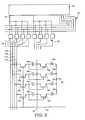
- FIG. 5shows a circuit diagram of the device of FIGS. 3 and 4;
- FIG. 6shows a schematic diagram of a multi-pixel device and its control apparatus
- FIGS. 7 and 8show plots of current through a pixel against time.
- an organic light-emitting devicehaving: an organic light-emitting region comprising a plurality of organic light-emitting pixels; switch means each associated with a respective pixel for switching power to that pixel; and drive means for driving each switch means to cycle between a first, low power mode and a second, high power mode, at a frequency sufficient to cause light emission from the associated pixel to appear substantially continuous, the duration of the high power mode relative to the low power mode being variable so as to vary the average brightness of the pixel.
- Each switch meanssuitably comprises at least one transistor. That transistor is preferably controlled by a gate voltage to switch power through the transistor and to the pixel. In the first mode the transistor preferably blocks current flow to the associated pixel so that pixel is substantially non-emissive. In the second mode the transistor preferably allows current flow to the associated pixel so that the pixel is substantially fully emissive. In the second mode the transistor is preferably in its fully on state. In the first mode the transistor is preferably in its fully off state.
- the brightness of the pixelis substantially insensitive to the transistor's characteristics, for example the gate voltage—so that small changes in the gate voltage do not substantially affect the through current to the pixel.
- the transistoris preferably a thin-film transistor.
- the switch meanspreferably comprises a charge storage means (e.g. a capacitor), suitably connected to the gate of the transistor described above, for holding the transistor in the first mode or the second mode.
- the charge storage meansis suitably charged by means of a second transistor, preferably a thin-film transistor.
- the switch meansis preferably a thin-film transistor switch means.
- the displayis preferably an active matrix display, most preferably a TFT active matrix display.
- the frequency of switching between the first and second modesis suitably greater than 30 Hz, preferably greater then 50 Hz and most preferably around 60 Hz or greater.
- the drive meansis preferably controllable to vary the duration of the high power mode relative to the low power mode.
- the duty cycle of the drive scheme(as measured by the duration of the second mode as a proportion of the total cycle time) may vary from zero (when the pixel is off) to 100% (maximum brightness).
- the high power modemay be provided as one or more than one discrete high power pulse
- Each pixelmay suitably comprise at least two independent light-emitting areas, with a switch means associated with each one of the light-emitting areas for independently switching power to that light-emitting area under the control of the drive means.
- the organic light-emitting devicemay comprise: an organic light-emitting region comprising a plurality of organic light-emitting pixels, each pixel comprising at least two independent light-emitting areas; a switch arrangement associated with each pixel and comprising switch means each associated with a respective light-emitting area of that pixel for switching power to that area; and a control means for addressing each pixel by its associated switch arrangement and controlling the brightness of each pixel by selectively driving one or more of the corresponding switch means to cause selected ones of the light-emitting areas of that pixel to emit light.
- each pixelis divided into separate light-emitting areas
- the light-emitting areas of each pixelare suitably of different sizes, preferably of different areas.
- every light-emitting area(except the smallest) is twice (or substantially twice) the size of the next-largest light-emitting area of that pixel.
- the drive meansis preferably capable of driving each pixel or each light-emitting area to operate non-instantaneously at an intermediate voltage, to allow further control over the brightness of the pixel. Therefore, the drive means is suitably capable of driving the switch means to a non-instantaneous partially on state.
- the partially on statemay be a third, intermediate power mode. Other intermediate power modes may also be provided.
- Preferred thicknesses for the pixels and/or light-emitting regionare in the range from 20 to 200 nm and most preferably around 100 nm.
- the organic light-emitting pixels and/or areasare suitably formed of a light-emitting polymer material, and preferably of a conjugated material.
- a suitable materialis a semiconductive conjugated polymer such as PPV or a derivative thereof.
- the light-emitting material of which the pixels and/or light-emitting areas are formedsuitably is or comprises PPV, poly(2-methoxy-5(2′-ethyl)hexyloxyphenylene-vinylene) (“MEH-PPV”), a PPV-derivative (e.g.
- a di-alkoxy or di-alkyl derivativea polyfluorene and/or a co-polymer incorporating polyfluorene segments, PPVs and/or related copolymers. It could be deposited by spin-coating, dip-coating, blade-coating, meniscus-coating, self-assembly etc.
- the constituent of the light-emitting region and/or its precursormay be water-based: examples are precursor-based PPVs.
- An altemabve materialis an organic molecular light-emitting material, e.g. Alq 3 , or any other small sublimed molecule or conjugated polymer electroluminescent material as known in the prior art.
- the organic light-emitting pixels and/or areasare suitably deposited by ink-jet printing.
- the conductive polymer layerpreferably comprises polyethylene dioxythiophene (“PEDT”), polystyrene sulphonic acid doped polyethylene dioxythiophene (“PEDT-PSS”), doped polyaniline, a doped alky 1 thiophene and/or a doped polypyrrole.
- the thickness of the layeris suitably less than 200 nm, preferably less than 100 nm and most preferably less than or around 50 nm.
- the sheet resistance of the layeris suitably greater than 10 6 or 10 7 Ohms/square, preferably greater than 10 8 Ohms/square and most preferably greater than or around 10 10 Ohms/square.
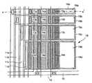
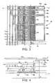
- FIGS. 3 to 5show the TFT circuitry associated with a pixel 16 of an organic light-emitting display device.
- the light emitting material of the pixelis divided into four light-emitting areas 19 a-d .
- the TFT circuitrycomprises a common line 12 (which corresponds to the electrode 3 in FIG. 1) and a scan line 10 (which corresponds to the electrode 6 ) which are shared by the light-emitting areas 19 a-d and other circuitry which is provided for each area individually.
- Each light-emitting areahas a signal line 11 a-d (which corresponds to the electrode 5 in FIG. 1 ), a switching transistor 13 a-d (which corresponds to the transistor 7 in FIG.
- a storage capacitor 14 a-d(which corresponds to the capacitor 8 in FIG. 1) and a current transistor 15 a-d (which corresponds to the transistor 9 in FIG. 1 ).
- Insulating regions of SiO 2shown in FIG. 4, separate the component parts of the circuitry, and the circuitry is deposited on a glass substrate 17 .
- electrode pads 18 a-d(see 18 a in FIG. 4) of transparent indium-tin oxide (“ITO”) to form the anodes of the emitting device.
- ITOtransparent indium-tin oxide
- the organic light-emitting material of the pixelis deposited on the pad in four separate sections (see 19 a-d in FIG. 4) and a common cathode 20 (corresponding to electrode 2 in FIG. 1) is deposited on top of those sections.
- Light emission from the pixel towards a vieweris generally in the direction into the page in FIG. 3 and as shown by arrow B in FIG. 4 .
- each light-emitting area 19 a-dcould be provided with an individual line equivalent to common line 12 , each individual line being controlled independently by the control units.
- the pixel of FIGS. 3 to 5forms part of a larger light-emitting device in which several thousand such pixels are arranged in orthogonal rows and columns. For instance, one typical size is 800 columns by 600 rows, giving a total of 480,000 pixels. The device could even be a colour display device having equal numbers of red, green and blue pixels.
- the additional units 50 in FIG. 5are for controlling another pixel.
- the TFT circuitryis first deposited on to the glass substrate 17 in the normal way. Then the organic light-emitting material is deposited on the ITO pads 18 d etc.
- the organic light-emitting material in this exampleis PPV.
- the PPVcould be deposited as a layer over the entire device (e.g. by spin-coating a precursor polyrner) and then patterned to form individual pixels or areas of pixels, or the pixels/areas could be deposited individually (e.g. by ink-jet printing), especially when forming a multi-colour (e.g. red/green/blue) device with pixels which each emit different colours of light.
- the resulting pixelsare around 1000 ⁇ thick.
- the materialis sprayed through an ink-jet printer spray head.
- a suitable spraying cycleis 14,400 drops per second, with a drop volume of 30 pl.
- FIG. 6shows schematically an example implementation of a completed device 21 having numerous pixels 22 , 23 etc. arranged in rows and columns, and each divided into a number of independently controllable light-emitting areas as illustrated in FIGS. 3 to 5 .
- a control unit 24is connected to the scan 25 and signal 26 lines and capable of controlling the voltage of each.
- the control unitreceives display signals at 27 (e.g. from a. personal computer) and comprises a processing means 28 for decoding those signals into real-time brightness information for each pixel of the display.
- the processor 28outputs address information on line 29 identifying each pixel in turn and brightness information on line 30 for that pixel.
- the brightness informationcould typically be: a number from zero to, say, 16 or 64 giving the desired brightness of the pixel.
- the control unitincludes an addressing switch unit 31 which receives address information at 32 identifying a pixel and brightness information at 33 , addresses the identified pixel by selecting the scan and signal lines at whose intersection the pixel lies and applies appropriate voltages to the scan and signal lines each to store on that pixel's storage capacitor the charge required to turn the pixel on to the desired brightness as indicated on line 33 .
- the control unit or any part of itcould be formed on the backplane of the display itself.
- the addressing switch 31could receive addressing and brightness information directly from the processor 28 .
- the intermediate processorreceives the brightness information for each pixel from processor 28 by lines 29 and 30 and stores the desired brightness of each pixel in memory 35 .
- the intermediate processorthen controls the addressing switch unit to fix the brightness of the pixels in one or both of two ways.
- the first way of fixing the brightnessis by turning the pixels on and off rapidly with a duty cycle that achieves the desired brightness from each pixel when averaged over time (for the duration of a cycle). For instance, if half-brightness is desired (e.g. a brightness of 32 in the 64 grey-scale scheme mentioned above) the pixel is switched so as to be fully on for half of the time and fully off for half of the time. An impression of flickering can be avoided by switching the pixel rapidly between its on and, off states. A suitable switching frequency to give a viewer an impression of constant light output from the device is 30 to 50 Hz or more.
- the brightness values output by the intermediate processor 34 on line 33indicate either fully on or fully off; intermediate values need not be used. Therefore, the current transistors of the pixels of the device are always (apart from transiently during turn-on and turn-off) operating in the predictable, flat on and off regions shown in FIG. 2, and the brightnesses of the pixels can more easily be made consistent.
- FIG. 8shows a plot of applied current against time for a single pixel.
- the lines 36separate cycles of the drive scheme. During the three cycles shown in FIG. 8 the brightness of the pixel is increased from around 10% to around 40%.
- the on-time of the pixelis applied as a series of pulses of equal length t p which, when added together, give the total on-time per cycle needed to achieve the required duty cycle. With the total on-time per cycle kept the same, the pattern of current between the on time and the off time can be varied to suit other requirements—e.g. to reduce flicker or cross-talk.
- the second way to fix the brightnessis to make use of the fact that the separate lightemitting areas of each pixel can be individually controlled.
- the brightness of the pixelcan be controlled by switching on one or more of the lightemitting areas. As before, the brightness is controlled by control unit 24 .
- the addressing switch 31again receives address information on line 32 identifying each pixel in turn and brightness information on line 33 for that pixel. This time the brightness information has a value from 0 to 16, indicating the desired brightness.
- the addressing switch 31includes a multi-area processor 45 which receives the address information for, say, the pixel shown in FIGS.
- 3 to 5identifies the scan and signal lines needed to address the individual light-emitting areas of that pixel and based on the brightness value received at 33 applies the appropriate voltages to those lines to turn none, one, two three or all of the light-emitting areas of the pixel fully on so as to achieve the desired brightness. Those selected areas can be left fully on until the brightness of the pixel is to be changed.
- the light-emifting areas into which each pixel is dividedcould be of the same size or of different sizes.
- One useful divisionis, where the pixel is to be divided into n light-emitting areas, for the sizes of those areas to be 1/(2 n ⁇ 1), 2/(2 n ⁇ 1), 4/(2 n ⁇ 1), . . . , (2 (n ⁇ 1) )/(2 n ⁇ 1) of the full size of the pixel.
- This arrangementprovides 2 n grey-scale values from those n pixels.
- the area of light-emitting area 19 dis twice that of area 19 c , which is twice that of area 19 b , which is twice that of area 19 a.
- the light-emitting areascould be defined as parallel strips running across the pixel, as in FIG. 3, or in other ways.
- the two ways of controlling brightness described abovecould be combined, so that a device having subdivided pixels of the type shown in FIGS. 3 to 5 is driven by a pulsed drive scheme as described with reference to FIG. 7 or 8 .
- Either or both of those two ways of controlling brightnesscould also be combined with voltage control, as described with reference to FIG. 1, where the voltage applied to each light-emitting area is also capable of being varied to a level that is not fully on or off, to give even more available grey levels.
- voltage controlas described with reference to FIG. 1
- the voltage applied to each light-emitting areais also capable of being varied to a level that is not fully on or off, to give even more available grey levels.
- the peak voltageis chosen from one of 16 levels, 4096 grey levels are available.
- a pulsed drive schemecould be applied to a device having unitary pixels, rather than the sub-divided pixels of the device of FIGS. 3 to 5 .
- the present inventionmay include any feature or combination of features disclosed herein either implicitly or explicitly or any generalisation thereof irrespective of whether it relates to the presently claimed invention.
Landscapes
- Engineering & Computer Science (AREA)
- Physics & Mathematics (AREA)
- Computer Hardware Design (AREA)
- General Physics & Mathematics (AREA)
- Theoretical Computer Science (AREA)
- Control Of Indicators Other Than Cathode Ray Tubes (AREA)
- Electroluminescent Light Sources (AREA)
Abstract
Description
Claims (19)
Applications Claiming Priority (3)
| Application Number | Priority Date | Filing Date | Title |
|---|---|---|---|
| GB9803441 | 1998-02-18 | ||
| GBGB9803441.6AGB9803441D0 (en) | 1998-02-18 | 1998-02-18 | Electroluminescent devices |
| PCT/GB1999/000383WO1999042983A1 (en) | 1998-02-18 | 1999-02-05 | Electroluminescent devices |
Related Parent Applications (1)
| Application Number | Title | Priority Date | Filing Date |
|---|---|---|---|
| PCT/GB1999/000383ContinuationWO1999042983A1 (en) | 1998-02-18 | 1999-02-05 | Electroluminescent devices |
Publications (1)
| Publication Number | Publication Date |
|---|---|
| US6429601B1true US6429601B1 (en) | 2002-08-06 |
Family
ID=10827208
Family Applications (1)
| Application Number | Title | Priority Date | Filing Date |
|---|---|---|---|
| US09/641,229Expired - LifetimeUS6429601B1 (en) | 1998-02-18 | 2000-08-17 | Electroluminescent devices |
Country Status (8)
| Country | Link |
|---|---|
| US (1) | US6429601B1 (en) |
| EP (1) | EP1057167B1 (en) |
| JP (1) | JP2002504717A (en) |
| KR (1) | KR100630788B1 (en) |
| CN (1) | CN1152360C (en) |
| AU (1) | AU2529099A (en) |
| GB (1) | GB9803441D0 (en) |
| WO (1) | WO1999042983A1 (en) |
Cited By (83)
| Publication number | Priority date | Publication date | Assignee | Title |
|---|---|---|---|---|
| US20030030601A1 (en)* | 2001-02-08 | 2003-02-13 | Naoaki Komiya | Organic EL circuit |
| US20030107537A1 (en)* | 2001-09-03 | 2003-06-12 | Pioneer Corporation | Capacitive light emitting device panel |
| US20030117347A1 (en)* | 2001-12-21 | 2003-06-26 | Koninklijke Philips Electronics N.V. | Active matrix electroluminescent display device |
| US20040100202A1 (en)* | 2001-03-22 | 2004-05-27 | Semiconductor Energy Laboratory Co., Ltd., A Japan Corporation | Light emitting device, driving method for the same and electronic apparatus |
| US6760004B2 (en)* | 2000-06-06 | 2004-07-06 | Semiconductor Energy Laboratory Co., Ltd. | Display device |
| US20040130517A1 (en)* | 2003-01-03 | 2004-07-08 | Chun-Huai Li | Pixel structure of active matrix display device |
| WO2004086347A2 (en) | 2003-03-25 | 2004-10-07 | Casio Computer Co., Ltd. | A drive device and a display device |
| US20040207577A1 (en)* | 2002-10-17 | 2004-10-21 | Nobuyuki Ito | Electroluminescent element and display |
| US20040263499A1 (en)* | 2002-11-29 | 2004-12-30 | Yoshifumi Tanada | Display device, driving method thereof, and electronic apparatus |
| GB2403841A (en)* | 2003-07-07 | 2005-01-12 | Pelikon Ltd | Control of Electroluminescent displays |
| US6897473B1 (en)* | 1998-03-13 | 2005-05-24 | Cambridge Display Technology Ltd. | Electroluminescent devices |
| WO2005062284A1 (en)* | 2003-12-09 | 2005-07-07 | Idc, Llc | Area array modulation and lead reduction in interferometric modulators |
| US20050200301A1 (en)* | 2000-12-21 | 2005-09-15 | Semiconductor Energy Laboratory Co., Ltd., A Japan Corporation | Light emitting device and method of manufacturing the same |
| US20050206991A1 (en)* | 2003-12-09 | 2005-09-22 | Clarence Chui | System and method for addressing a MEMS display |
| US20050263771A1 (en)* | 2000-12-11 | 2005-12-01 | Semiconductor Energy Laboratory Co., Ltd., A Japan Corporation | Semiconductor device, and manufacturing method thereof |
| US20060039051A1 (en)* | 2004-07-28 | 2006-02-23 | Sony Corporation | Hologram apparatus, positioning method for spatial light modulator and image pickup device, and hologram recording material |
| US20060066525A1 (en)* | 2002-11-23 | 2006-03-30 | Koninklijke Philips Electronics, N.V. | Colour control for active matrix electroluminescent display |
| US20060067653A1 (en)* | 2004-09-27 | 2006-03-30 | Gally Brian J | Method and system for driving interferometric modulators |
| US20060077127A1 (en)* | 2004-09-27 | 2006-04-13 | Sampsell Jeffrey B | Controller and driver features for bi-stable display |
| US20060092218A1 (en)* | 2004-11-04 | 2006-05-04 | Applied Materials, Inc. | Methods and apparatus for inkjet printing |
| US20060093751A1 (en)* | 2004-11-04 | 2006-05-04 | Applied Materials, Inc. | System and methods for inkjet printing for flat panel displays |
| US20060092207A1 (en)* | 2004-11-04 | 2006-05-04 | Bassam Shamoun | Methods and apparatus for precision control of print head assemblies |
| US20060092199A1 (en)* | 2004-11-04 | 2006-05-04 | White John M | Methods and apparatus for aligning print heads |
| US20060134939A1 (en)* | 2004-03-01 | 2006-06-22 | Anritsu Company | Method for forming hermetic glass bead assembly having high frequency compensation |
| US20060132028A1 (en)* | 2004-12-16 | 2006-06-22 | Lexmark International, Inc. | Electroluminescent display construction using printing technology |
| US7136213B2 (en) | 2004-09-27 | 2006-11-14 | Idc, Llc | Interferometric modulators having charge persistence |
| US20060279480A1 (en)* | 2003-07-18 | 2006-12-14 | Koninklijke Philips Electronics N.V. | Oled display device |
| US20060284894A1 (en)* | 2003-08-27 | 2006-12-21 | Johnson Mark T | Display device |
| US20070046603A1 (en)* | 2004-09-30 | 2007-03-01 | Smith Euan C | Multi-line addressing methods and apparatus |
| US20070069992A1 (en)* | 2004-09-30 | 2007-03-29 | Smith Euan C | Multi-line addressing methods and apparatus |
| US20070085779A1 (en)* | 2004-09-30 | 2007-04-19 | Smith Euan C | Multi-line addressing methods and apparatus |
| US20070215883A1 (en)* | 2006-03-20 | 2007-09-20 | Dixon Michael J | Electroluminescent Devices, Subassemblies for use in Making Electroluminescent Devices, and Dielectric Materials, Conductive Inks and Substrates Related Thereto |
| US7310179B2 (en) | 2004-09-27 | 2007-12-18 | Idc, Llc | Method and device for selective adjustment of hysteresis window |
| US20080018632A1 (en)* | 2004-06-22 | 2008-01-24 | Koninklijke Philips Electronics, N.V. | Driving To Reduce Aging In An Active Matrix Led Display |
| US20080062093A1 (en)* | 2002-04-24 | 2008-03-13 | Seiko Epson Corporation | Electronic apparatus, electronic system, and driving method for electronic apparatus |
| US7345805B2 (en) | 2004-09-27 | 2008-03-18 | Idc, Llc | Interferometric modulator array with integrated MEMS electrical switches |
| US7355779B2 (en) | 2005-09-02 | 2008-04-08 | Idc, Llc | Method and system for driving MEMS display elements |
| US7388706B2 (en) | 1995-05-01 | 2008-06-17 | Idc, Llc | Photonic MEMS and structures |
| US20080266333A1 (en)* | 2007-01-29 | 2008-10-30 | Qualcomm Mems Technologies, Inc. | Hybrid color synthesis for multistate reflective modular displays |
| US7446927B2 (en) | 2004-09-27 | 2008-11-04 | Idc, Llc | MEMS switch with set and latch electrodes |
| US20080273024A1 (en)* | 2002-12-18 | 2008-11-06 | Semiconductor Energy Laboratory Co., Ltd. | Display Device and Driving Method Thereof |
| US20080291122A1 (en)* | 2004-12-23 | 2008-11-27 | Euan Christopher Smith | Digital Signal Processing Methods and Apparatus |
| US7471444B2 (en) | 1996-12-19 | 2008-12-30 | Idc, Llc | Interferometric modulation of radiation |
| US7486429B2 (en) | 2004-09-27 | 2009-02-03 | Idc, Llc | Method and device for multistate interferometric light modulation |
| US7499208B2 (en) | 2004-08-27 | 2009-03-03 | Udc, Llc | Current mode display driver circuit realization feature |
| US7515147B2 (en) | 2004-08-27 | 2009-04-07 | Idc, Llc | Staggered column drive circuit systems and methods |
| US7532195B2 (en) | 2004-09-27 | 2009-05-12 | Idc, Llc | Method and system for reducing power consumption in a display |
| US20090121983A1 (en)* | 2007-11-13 | 2009-05-14 | Samsung Electronics Co., Ltd. | Organic light emitting diode display and method for manufacturing the same |
| US7545550B2 (en) | 2004-09-27 | 2009-06-09 | Idc, Llc | Systems and methods of actuating MEMS display elements |
| US7551159B2 (en) | 2004-08-27 | 2009-06-23 | Idc, Llc | System and method of sensing actuation and release voltages of an interferometric modulator |
| US7560299B2 (en) | 2004-08-27 | 2009-07-14 | Idc, Llc | Systems and methods of actuating MEMS display elements |
| US20090201318A1 (en)* | 2008-02-13 | 2009-08-13 | Qualcomm Mems Technologies, Inc. | Multi-level stochastic dithering with noise mitigation via sequential template averaging |
| US7611217B2 (en) | 2005-09-29 | 2009-11-03 | Applied Materials, Inc. | Methods and systems for inkjet drop positioning |
| US7626581B2 (en) | 2004-09-27 | 2009-12-01 | Idc, Llc | Device and method for display memory using manipulation of mechanical response |
| US20090315814A1 (en)* | 2008-06-18 | 2009-12-24 | Sony Corporation | Self-light emitting display unit and electronic device |
| US7637587B2 (en) | 2007-08-29 | 2009-12-29 | Applied Materials, Inc. | System and method for reliability testing and troubleshooting inkjet printers |
| US7702192B2 (en) | 2006-06-21 | 2010-04-20 | Qualcomm Mems Technologies, Inc. | Systems and methods for driving MEMS display |
| US7724993B2 (en) | 2004-09-27 | 2010-05-25 | Qualcomm Mems Technologies, Inc. | MEMS switches with deforming membranes |
| US7777715B2 (en) | 2006-06-29 | 2010-08-17 | Qualcomm Mems Technologies, Inc. | Passive circuits for de-multiplexing display inputs |
| US7791571B2 (en) | 2004-04-22 | 2010-09-07 | Semiconductor Energy Laboratory Co., Ltd. | Light emitting device and driving method of the same |
| US7843410B2 (en) | 2004-09-27 | 2010-11-30 | Qualcomm Mems Technologies, Inc. | Method and device for electrically programmable display |
| US7857413B2 (en) | 2007-03-01 | 2010-12-28 | Applied Materials, Inc. | Systems and methods for controlling and testing jetting stability in inkjet print heads |
| US20100328365A1 (en)* | 2009-06-30 | 2010-12-30 | Canon Kabushiki Kaisha | Semiconductor device |
| US20110032427A1 (en)* | 2009-06-05 | 2011-02-10 | Qualcomm Mems Technologies, Inc. | System and method for improving the quality of halftone video using a fixed threshold |
| US7889163B2 (en) | 2004-08-27 | 2011-02-15 | Qualcomm Mems Technologies, Inc. | Drive method for MEMS devices |
| US7920136B2 (en) | 2005-05-05 | 2011-04-05 | Qualcomm Mems Technologies, Inc. | System and method of driving a MEMS display device |
| US7923057B2 (en) | 2006-02-07 | 2011-04-12 | Applied Materials, Inc. | Methods and apparatus for reducing irregularities in color filters |
| US7948457B2 (en) | 2005-05-05 | 2011-05-24 | Qualcomm Mems Technologies, Inc. | Systems and methods of actuating MEMS display elements |
| US8049713B2 (en) | 2006-04-24 | 2011-11-01 | Qualcomm Mems Technologies, Inc. | Power consumption optimized display update |
| US8174469B2 (en) | 2005-05-05 | 2012-05-08 | Qualcomm Mems Technologies, Inc. | Dynamic driver IC and display panel configuration |
| US8194056B2 (en) | 2006-02-09 | 2012-06-05 | Qualcomm Mems Technologies Inc. | Method and system for writing data to MEMS display elements |
| US8310441B2 (en) | 2004-09-27 | 2012-11-13 | Qualcomm Mems Technologies, Inc. | Method and system for writing data to MEMS display elements |
| WO2013007965A1 (en)* | 2011-07-08 | 2013-01-17 | Cambridge Display Technology Limited | Pixel driver circuit for organic electro - luminescent display |
| US8391630B2 (en) | 2005-12-22 | 2013-03-05 | Qualcomm Mems Technologies, Inc. | System and method for power reduction when decompressing video streams for interferometric modulator displays |
| US8736520B2 (en) | 1999-10-21 | 2014-05-27 | Semiconductor Energy Laboratory Co., Ltd. | Electro-optical device |
| US8736590B2 (en) | 2009-03-27 | 2014-05-27 | Qualcomm Mems Technologies, Inc. | Low voltage driver scheme for interferometric modulators |
| US8878825B2 (en) | 2004-09-27 | 2014-11-04 | Qualcomm Mems Technologies, Inc. | System and method for providing a variable refresh rate of an interferometric modulator display |
| US8928967B2 (en) | 1998-04-08 | 2015-01-06 | Qualcomm Mems Technologies, Inc. | Method and device for modulating light |
| US8971675B2 (en) | 2006-01-13 | 2015-03-03 | Qualcomm Mems Technologies, Inc. | Interconnect structure for MEMS device |
| US9110289B2 (en) | 1998-04-08 | 2015-08-18 | Qualcomm Mems Technologies, Inc. | Device for modulating light with multiple electrodes |
| US20160189663A1 (en)* | 2014-12-29 | 2016-06-30 | Samsung Display Co., Ltd | Organic light-emitting display and method of driving the same |
| US20180053460A1 (en)* | 2016-08-19 | 2018-02-22 | Innolux Corporation | Light-emitting device (led) and led displaying circuit |
| US20250239212A1 (en)* | 2023-12-25 | 2025-07-24 | Nichia Corporation | Light-emitting device and method for driving the same |
Families Citing this family (40)
| Publication number | Priority date | Publication date | Assignee | Title |
|---|---|---|---|---|
| US6839158B2 (en) | 1997-08-28 | 2005-01-04 | E Ink Corporation | Encapsulated electrophoretic displays having a monolayer of capsules and materials and methods for making the same |
| JP2002535722A (en)* | 1999-01-21 | 2002-10-22 | コーニンクレッカ フィリップス エレクトロニクス エヌ ヴィ | Organic light emitting display |
| JP4353300B2 (en)* | 1999-06-17 | 2009-10-28 | ソニー株式会社 | Image display apparatus and driving method thereof |
| EP1196814A1 (en)* | 1999-07-21 | 2002-04-17 | E Ink Corporation | Use of a storage capacitor to enhance the performance of an active matrix driven electronic display |
| JP2001085159A (en)* | 1999-09-13 | 2001-03-30 | Sanyo Electric Co Ltd | Organic electroluminescent element driving method, driving device, and display device using it |
| TW522453B (en) | 1999-09-17 | 2003-03-01 | Semiconductor Energy Lab | Display device |
| TW587239B (en) | 1999-11-30 | 2004-05-11 | Semiconductor Energy Lab | Electric device |
| KR100327375B1 (en) | 2000-03-06 | 2002-03-06 | 구자홍 | apparatus for active driver |
| TW508545B (en)* | 2000-03-30 | 2002-11-01 | Seiko Epson Corp | Display apparatus |
| TW493153B (en) | 2000-05-22 | 2002-07-01 | Koninkl Philips Electronics Nv | Display device |
| JP3475938B2 (en)* | 2000-05-26 | 2003-12-10 | セイコーエプソン株式会社 | Electro-optical device driving method, electro-optical device driving circuit, electro-optical device, and electronic apparatus |
| CN100541813C (en) | 2000-06-23 | 2009-09-16 | 剑桥显示技术有限公司 | Light emitting device |
| JP4538915B2 (en)* | 2000-07-24 | 2010-09-08 | セイコーエプソン株式会社 | Driving method of electro-optical device |
| JP4945731B2 (en)* | 2000-09-11 | 2012-06-06 | 奇美電子股▲ふん▼有限公司 | Matrix display device |
| GB2367413A (en)* | 2000-09-28 | 2002-04-03 | Seiko Epson Corp | Organic electroluminescent display device |
| US7315295B2 (en) | 2000-09-29 | 2008-01-01 | Seiko Epson Corporation | Driving method for electro-optical device, electro-optical device, and electronic apparatus |
| JP3797174B2 (en)* | 2000-09-29 | 2006-07-12 | セイコーエプソン株式会社 | Electro-optical device, driving method thereof, and electronic apparatus |
| US6580657B2 (en) | 2001-01-04 | 2003-06-17 | International Business Machines Corporation | Low-power organic light emitting diode pixel circuit |
| JP2002358031A (en) | 2001-06-01 | 2002-12-13 | Semiconductor Energy Lab Co Ltd | Light emitting device and driving method thereof |
| US7034339B2 (en)* | 2001-08-09 | 2006-04-25 | Idemitsu Kosan Co., Ltd. | Organic EL display device having host compound and phosphorescent luminous compound, and method of driving same |
| GB2379317A (en) | 2001-08-30 | 2003-03-05 | Cambridge Display Tech Ltd | Optoelectronic display operating by photoluminescence quenching |
| GB2381644A (en) | 2001-10-31 | 2003-05-07 | Cambridge Display Tech Ltd | Display drivers |
| GB2381643A (en) | 2001-10-31 | 2003-05-07 | Cambridge Display Tech Ltd | Display drivers |
| AU2002352830A1 (en)* | 2001-11-20 | 2003-06-23 | International Business Machines Corporation | Active matrix organic light-emitting-diodes with amorphous silicon transistors |
| GB0128419D0 (en)* | 2001-11-28 | 2002-01-16 | Koninkl Philips Electronics Nv | Electroluminescent display device |
| JP4707011B2 (en)* | 2002-04-24 | 2011-06-22 | セイコーエプソン株式会社 | Electro-optical device and driving method thereof |
| GB2389951A (en) | 2002-06-18 | 2003-12-24 | Cambridge Display Tech Ltd | Display driver circuits for active matrix OLED displays |
| GB2389952A (en) | 2002-06-18 | 2003-12-24 | Cambridge Display Tech Ltd | Driver circuits for electroluminescent displays with reduced power consumption |
| JP4574127B2 (en) | 2003-03-26 | 2010-11-04 | 株式会社半導体エネルギー研究所 | Element substrate and light emitting device |
| GB2410600A (en) | 2004-01-30 | 2005-08-03 | Cambridge Display Tech Ltd | Organic light emitting diode display device |
| CN100534242C (en)* | 2005-08-24 | 2009-08-26 | 中华映管股份有限公司 | Organic electroluminescent display device |
| GB2430069A (en) | 2005-09-12 | 2007-03-14 | Cambridge Display Tech Ltd | Active matrix display drive control systems |
| GB2437113B (en) | 2006-04-12 | 2008-11-26 | Cambridge Display Tech Ltd | Light-emissive display and method of manufacturing the same |
| GB2441355B (en) | 2006-08-31 | 2009-05-20 | Cambridge Display Tech Ltd | Organic electronic device |
| GB2448175B (en) | 2007-04-04 | 2009-07-22 | Cambridge Display Tech Ltd | Thin film transistor |
| GB0721567D0 (en) | 2007-11-02 | 2007-12-12 | Cambridge Display Tech Ltd | Pixel driver circuits |
| GB2460018B (en) | 2008-05-07 | 2013-01-30 | Cambridge Display Tech Ltd | Active matrix displays |
| GB2462296A (en) | 2008-08-01 | 2010-02-03 | Cambridge Display Tech Ltd | Pixel driver circuits |
| GB2462646B (en) | 2008-08-15 | 2011-05-11 | Cambridge Display Tech Ltd | Active matrix displays |
| KR101758297B1 (en)* | 2010-06-04 | 2017-07-26 | 가부시키가이샤 한도오따이 에네루기 켄큐쇼 | Display device and electronic device |
Citations (13)
| Publication number | Priority date | Publication date | Assignee | Title |
|---|---|---|---|---|
| US4074318A (en) | 1976-12-13 | 1978-02-14 | Bell Telephone Laboratories, Incorporated | Led array imaging system-serial approach |
| JPS58220185A (en) | 1982-06-17 | 1983-12-21 | セイコーインスツルメンツ株式会社 | Display element |
| US4539507A (en) | 1983-03-25 | 1985-09-03 | Eastman Kodak Company | Organic electroluminescent devices having improved power conversion efficiencies |
| US5235253A (en)* | 1990-11-27 | 1993-08-10 | Fuji Xerox Co., Ltd. | Thin-film electroluminescent device drive circuit |
| EP0595792A2 (en) | 1988-06-07 | 1994-05-04 | Sharp Kabushiki Kaisha | Method and apparatus for driving capacitive display device |
| JPH07122360A (en) | 1993-10-22 | 1995-05-12 | Mitsubishi Chem Corp | Organic electroluminescent panel and driving method thereof |
| EP0762374A1 (en) | 1995-08-21 | 1997-03-12 | Motorola, Inc. | Active driven led matrices |
| US5684365A (en)* | 1994-12-14 | 1997-11-04 | Eastman Kodak Company | TFT-el display panel using organic electroluminescent media |
| US5714968A (en) | 1994-08-09 | 1998-02-03 | Nec Corporation | Current-dependent light-emitting element drive circuit for use in active matrix display device |
| WO1999012150A1 (en) | 1997-08-28 | 1999-03-11 | Seiko Epson Corproration | Display device |
| US5923309A (en)* | 1996-05-15 | 1999-07-13 | Pioneer Electronic Corporation | Display device using current driven type light emitting elements |
| US6099980A (en)* | 1996-07-16 | 2000-08-08 | U.S. Philips Corporation | Organic electroluminescent device |
| US6157356A (en)* | 1996-04-12 | 2000-12-05 | International Business Machines Company | Digitally driven gray scale operation of active matrix OLED displays |
Family Cites Families (15)
| Publication number | Priority date | Publication date | Assignee | Title |
|---|---|---|---|---|
| JPS6122326A (en)* | 1984-03-23 | 1986-01-30 | Citizen Watch Co Ltd | Gradational display device |
| JPH0422618Y2 (en)* | 1986-10-09 | 1992-05-25 | ||
| JPH04102830A (en)* | 1990-08-22 | 1992-04-03 | Hitachi Ltd | multicolor lcd display panel |
| JPH0535207A (en)* | 1991-08-02 | 1993-02-12 | Fuji Xerox Co Ltd | El driving device |
| JPH06161385A (en)* | 1992-11-25 | 1994-06-07 | Hitachi Ltd | Active matrix display |
| FR2703814B1 (en)* | 1993-04-08 | 1995-07-07 | Sagem | COLOR MATRIX DISPLAY. |
| JPH06324306A (en)* | 1993-05-11 | 1994-11-25 | Toshiba Corp | Liquid crystal display device |
| US5594463A (en)* | 1993-07-19 | 1997-01-14 | Pioneer Electronic Corporation | Driving circuit for display apparatus, and method of driving display apparatus |
| JP3526471B2 (en)* | 1994-06-09 | 2004-05-17 | 株式会社東芝 | Multi-tone display device |
| GB9407116D0 (en)* | 1994-04-11 | 1994-06-01 | Secr Defence | Ferroelectric liquid crystal display with greyscale |
| JP2689916B2 (en)* | 1994-08-09 | 1997-12-10 | 日本電気株式会社 | Active matrix type current control type light emitting element drive circuit |
| JP2678574B2 (en)* | 1994-10-04 | 1997-11-17 | 近畿日本鉄道株式会社 | Light control device |
| JP3075335B2 (en)* | 1995-07-14 | 2000-08-14 | 日本放送協会 | Halftone display method |
| JP2941704B2 (en)* | 1996-04-16 | 1999-08-30 | ローム株式会社 | Light emitting element drive circuit |
| JP2720943B2 (en)* | 1996-12-25 | 1998-03-04 | 富士通株式会社 | Gray scale driving method for flat display device |
- 1998
- 1998-02-18GBGBGB9803441.6Apatent/GB9803441D0/ennot_activeCeased
- 1999
- 1999-02-05WOPCT/GB1999/000383patent/WO1999042983A1/enactiveIP Right Grant
- 1999-02-05EPEP99904974Apatent/EP1057167B1/ennot_activeExpired - Lifetime
- 1999-02-05KRKR1020007009072Apatent/KR100630788B1/ennot_activeExpired - Lifetime
- 1999-02-05AUAU25290/99Apatent/AU2529099A/ennot_activeAbandoned
- 1999-02-05JPJP2000532839Apatent/JP2002504717A/enactivePending
- 1999-02-05CNCNB998031275Apatent/CN1152360C/ennot_activeExpired - Lifetime
- 2000
- 2000-08-17USUS09/641,229patent/US6429601B1/ennot_activeExpired - Lifetime
Patent Citations (13)
| Publication number | Priority date | Publication date | Assignee | Title |
|---|---|---|---|---|
| US4074318A (en) | 1976-12-13 | 1978-02-14 | Bell Telephone Laboratories, Incorporated | Led array imaging system-serial approach |
| JPS58220185A (en) | 1982-06-17 | 1983-12-21 | セイコーインスツルメンツ株式会社 | Display element |
| US4539507A (en) | 1983-03-25 | 1985-09-03 | Eastman Kodak Company | Organic electroluminescent devices having improved power conversion efficiencies |
| EP0595792A2 (en) | 1988-06-07 | 1994-05-04 | Sharp Kabushiki Kaisha | Method and apparatus for driving capacitive display device |
| US5235253A (en)* | 1990-11-27 | 1993-08-10 | Fuji Xerox Co., Ltd. | Thin-film electroluminescent device drive circuit |
| JPH07122360A (en) | 1993-10-22 | 1995-05-12 | Mitsubishi Chem Corp | Organic electroluminescent panel and driving method thereof |
| US5714968A (en) | 1994-08-09 | 1998-02-03 | Nec Corporation | Current-dependent light-emitting element drive circuit for use in active matrix display device |
| US5684365A (en)* | 1994-12-14 | 1997-11-04 | Eastman Kodak Company | TFT-el display panel using organic electroluminescent media |
| EP0762374A1 (en) | 1995-08-21 | 1997-03-12 | Motorola, Inc. | Active driven led matrices |
| US6157356A (en)* | 1996-04-12 | 2000-12-05 | International Business Machines Company | Digitally driven gray scale operation of active matrix OLED displays |
| US5923309A (en)* | 1996-05-15 | 1999-07-13 | Pioneer Electronic Corporation | Display device using current driven type light emitting elements |
| US6099980A (en)* | 1996-07-16 | 2000-08-08 | U.S. Philips Corporation | Organic electroluminescent device |
| WO1999012150A1 (en) | 1997-08-28 | 1999-03-11 | Seiko Epson Corproration | Display device |
Non-Patent Citations (1)
| Title |
|---|
| "Photoconductive Polymers", Encyclopedia of Chemical Technology, Fourth Edition, vol. 18, p. 857. |
Cited By (178)
| Publication number | Priority date | Publication date | Assignee | Title |
|---|---|---|---|---|
| US7388706B2 (en) | 1995-05-01 | 2008-06-17 | Idc, Llc | Photonic MEMS and structures |
| US7471444B2 (en) | 1996-12-19 | 2008-12-30 | Idc, Llc | Interferometric modulation of radiation |
| US8115199B2 (en) | 1998-03-13 | 2012-02-14 | Cambridge Display Technology Ltd. | Electroluminescent devices |
| US20060246613A1 (en)* | 1998-03-13 | 2006-11-02 | Cambridge Display Technology Ltd. | Electroluminescent devices |
| US20060263917A1 (en)* | 1998-03-13 | 2006-11-23 | Cambridge Display Technology Ltd. | Electroluminescent devices |
| US7227180B2 (en) | 1998-03-13 | 2007-06-05 | Cambridge Display Technology Ltd. | Electroluminescent devices |
| US7393704B2 (en) | 1998-03-13 | 2008-07-01 | Cambridge Display Tech Ltd | Electroluminescent devices |
| US20050184658A1 (en)* | 1998-03-13 | 2005-08-25 | Cambridge Display Technology Ltd. | Electroluminescent devices |
| US7449714B2 (en) | 1998-03-13 | 2008-11-11 | Cambridge Display Technology Ltd. | Electroluminescent devices |
| US6897473B1 (en)* | 1998-03-13 | 2005-05-24 | Cambridge Display Technology Ltd. | Electroluminescent devices |
| US8928967B2 (en) | 1998-04-08 | 2015-01-06 | Qualcomm Mems Technologies, Inc. | Method and device for modulating light |
| US9110289B2 (en) | 1998-04-08 | 2015-08-18 | Qualcomm Mems Technologies, Inc. | Device for modulating light with multiple electrodes |
| US8736520B2 (en) | 1999-10-21 | 2014-05-27 | Semiconductor Energy Laboratory Co., Ltd. | Electro-optical device |
| US8289241B2 (en) | 2000-06-06 | 2012-10-16 | Semiconductor Energy Laboratory Co., Ltd. | Display device |
| US20040239607A1 (en)* | 2000-06-06 | 2004-12-02 | Semiconductor Energy Laboratory Co., Ltd., A Japan Corporation | Display device |
| US8659516B2 (en) | 2000-06-06 | 2014-02-25 | Semiconductor Energy Laboratory Co., Ltd. | Display device |
| US6760004B2 (en)* | 2000-06-06 | 2004-07-06 | Semiconductor Energy Laboratory Co., Ltd. | Display device |
| US7742020B2 (en) | 2000-06-06 | 2010-06-22 | Semiconductor Energy Laboratory Co., Ltd. | Display device |
| US20100245302A1 (en)* | 2000-06-06 | 2010-09-30 | Semiconductor Energy Laboratory Co., Ltd. | Display device |
| US8421135B2 (en) | 2000-12-11 | 2013-04-16 | Semiconductor Energy Laboratory Co., Ltd. | Semiconductor device, and manufacturing method thereof |
| US7459352B2 (en) | 2000-12-11 | 2008-12-02 | Semiconductor Energy Laboratory Co., Ltd. | Semiconductor device, and manufacturing method thereof |
| US10665610B2 (en) | 2000-12-11 | 2020-05-26 | Semiconductor Energy Laboratory Co., Ltd. | Semiconductor device, and manufacturing method thereof |
| US20050263771A1 (en)* | 2000-12-11 | 2005-12-01 | Semiconductor Energy Laboratory Co., Ltd., A Japan Corporation | Semiconductor device, and manufacturing method thereof |
| US9059216B2 (en) | 2000-12-11 | 2015-06-16 | Semiconductor Energy Laboratory Co., Ltd. | Semiconductor device, and manufacturing method thereof |
| US20090146149A1 (en)* | 2000-12-11 | 2009-06-11 | Semiconductor Energy Laboratory Co., Ltd. | Semiconductor device, and manufacturing method thereof |
| US9666601B2 (en) | 2000-12-11 | 2017-05-30 | Semiconductor Energy Laboratory Co., Ltd. | Semiconductor device, and manufacturing method thereof |
| US7629618B2 (en) | 2000-12-21 | 2009-12-08 | Semiconductor Energy Laboratory Co., Ltd. | Light emitting device and method of manufacturing the same |
| US20090321753A1 (en)* | 2000-12-21 | 2009-12-31 | Semiconductor Energy Laboratory Co., Ltd. | Light Emitting Device and Method of Manufacturing the Same |
| US9793335B2 (en) | 2000-12-21 | 2017-10-17 | Semiconductor Energy Laboratory Co., Ltd. | Light emitting device and method of manufacturing the same |
| US9231044B2 (en) | 2000-12-21 | 2016-01-05 | Semiconductor Energy Laboratory Co., Ltd. | Light emitting device and method of manufacturing the same |
| US20050200301A1 (en)* | 2000-12-21 | 2005-09-15 | Semiconductor Energy Laboratory Co., Ltd., A Japan Corporation | Light emitting device and method of manufacturing the same |
| US8013346B2 (en) | 2000-12-21 | 2011-09-06 | Semiconductor Energy Laboratory Co., Ltd. | Light emitting device and method of manufacturing the same |
| US8735909B2 (en) | 2000-12-21 | 2014-05-27 | Semiconductor Energy Laboratory Co., Ltd. | Light emitting device and method of manufacturing the same |
| US6954190B2 (en)* | 2001-02-08 | 2005-10-11 | Sanyo Electric Co., Ltd. | Organic EL circuit |
| US20030030601A1 (en)* | 2001-02-08 | 2003-02-13 | Naoaki Komiya | Organic EL circuit |
| US8593066B2 (en) | 2001-03-22 | 2013-11-26 | Semiconductor Energy Laboratory Co., Ltd. | Light emitting device, driving method for same and electronic apparatus |
| US20070007527A1 (en)* | 2001-03-22 | 2007-01-11 | Semiconductor Energy Laboratory Co., Ltd. | Light Emitting Device, Driving Method for the Same and Electronic Apparatus |
| US7545353B2 (en) | 2001-03-22 | 2009-06-09 | Semiconductor Energy Laboratory Co., Ltd. | Light emitting device, driving method for the same and electronic apparatus |
| US20100006866A1 (en)* | 2001-03-22 | 2010-01-14 | Semiconductor Energy Laboratory Co., Ltd. | Light emitting device, driving method for the same and electronic apparatus |
| US20040100202A1 (en)* | 2001-03-22 | 2004-05-27 | Semiconductor Energy Laboratory Co., Ltd., A Japan Corporation | Light emitting device, driving method for the same and electronic apparatus |
| US6914390B2 (en) | 2001-03-22 | 2005-07-05 | Semiconductor Energy Laboratory Co., Ltd. | Light emitting device, driving method for the same and electronic apparatus |
| US7106006B2 (en) | 2001-03-22 | 2006-09-12 | Semiconductor Energy Laboratory Co., Ltd. | Light emitting device, driving method for the same and electronic apparatus |
| US20050218400A1 (en)* | 2001-03-22 | 2005-10-06 | Semiconductor Energy Laboratory Co., Ltd., A Japan Corporation | Light emitting device, driving method for the same and electronic apparatus |
| US7990350B2 (en) | 2001-03-22 | 2011-08-02 | Semiconductor Energy Laboratory Co., Ltd. | Light emitting device, driving method for the same and electronic apparatus |
| US20030107537A1 (en)* | 2001-09-03 | 2003-06-12 | Pioneer Corporation | Capacitive light emitting device panel |
| US20030117347A1 (en)* | 2001-12-21 | 2003-06-26 | Koninklijke Philips Electronics N.V. | Active matrix electroluminescent display device |
| US20080062093A1 (en)* | 2002-04-24 | 2008-03-13 | Seiko Epson Corporation | Electronic apparatus, electronic system, and driving method for electronic apparatus |
| US8194011B2 (en) | 2002-04-24 | 2012-06-05 | Seiko Epson Corporation | Electronic apparatus, electronic system, and driving method for electronic apparatus |
| US7215305B2 (en)* | 2002-10-17 | 2007-05-08 | Dai Nippon Printing Co., Ltd. | Electroluminescent element and display |
| US20040207577A1 (en)* | 2002-10-17 | 2004-10-21 | Nobuyuki Ito | Electroluminescent element and display |
| US20060066525A1 (en)* | 2002-11-23 | 2006-03-30 | Koninklijke Philips Electronics, N.V. | Colour control for active matrix electroluminescent display |
| US7403177B2 (en) | 2002-11-29 | 2008-07-22 | Semiconductor Energy Laboratory Co., Ltd. | Display device, driving method thereof, and electronic apparatus |
| EP1580718A4 (en)* | 2002-11-29 | 2006-03-29 | Semiconductor Energy Lab | Display and its driving method, and electronic device |
| US20040263499A1 (en)* | 2002-11-29 | 2004-12-30 | Yoshifumi Tanada | Display device, driving method thereof, and electronic apparatus |
| US20080273024A1 (en)* | 2002-12-18 | 2008-11-06 | Semiconductor Energy Laboratory Co., Ltd. | Display Device and Driving Method Thereof |
| US20040130517A1 (en)* | 2003-01-03 | 2004-07-08 | Chun-Huai Li | Pixel structure of active matrix display device |
| WO2004086347A2 (en) | 2003-03-25 | 2004-10-07 | Casio Computer Co., Ltd. | A drive device and a display device |
| CN100435200C (en)* | 2003-03-25 | 2008-11-19 | 卡西欧计算机株式会社 | Driving apparatus and display apparatus |
| WO2004086347A3 (en)* | 2003-03-25 | 2004-12-02 | Casio Computer Co Ltd | A drive device and a display device |
| US7855699B2 (en) | 2003-03-25 | 2010-12-21 | Casio Computer Co., Ltd. | Drive device and a display device |
| US20060017668A1 (en)* | 2003-03-25 | 2006-01-26 | Casio Computer Co., Ltd. | Drive device and a display device |
| GB2403841B (en)* | 2003-07-07 | 2006-08-09 | Pelikon Ltd | Control of Electroluminescent displays |
| GB2403841A (en)* | 2003-07-07 | 2005-01-12 | Pelikon Ltd | Control of Electroluminescent displays |
| US20060279480A1 (en)* | 2003-07-18 | 2006-12-14 | Koninklijke Philips Electronics N.V. | Oled display device |
| US8294641B2 (en)* | 2003-07-18 | 2012-10-23 | Koninklijke Philips Electronics N.V. | OLED display device |
| US20060284894A1 (en)* | 2003-08-27 | 2006-12-21 | Johnson Mark T | Display device |
| US8207928B2 (en)* | 2003-08-27 | 2012-06-26 | Koninklijke Philips Electronics N.V. | Method for controlling pixel brightness in a display device |
| US7196837B2 (en) | 2003-12-09 | 2007-03-27 | Idc, Llc | Area array modulation and lead reduction in interferometric modulators |
| US7864402B2 (en) | 2003-12-09 | 2011-01-04 | Qualcomm Mems Technologies, Inc. | MEMS display |
| US20050206991A1 (en)* | 2003-12-09 | 2005-09-22 | Clarence Chui | System and method for addressing a MEMS display |
| US20080252959A1 (en)* | 2003-12-09 | 2008-10-16 | Clarence Chui | Mems display |
| US20070291347A1 (en)* | 2003-12-09 | 2007-12-20 | Sampsell Jeffrey B | Area array modulation and lead reduction in interferometric modulators |
| US7489428B2 (en) | 2003-12-09 | 2009-02-10 | Idc, Llc | Area array modulation and lead reduction in interferometric modulators |
| US7782525B2 (en) | 2003-12-09 | 2010-08-24 | Qualcomm Mems Technologies, Inc. | Area array modulation and lead reduction in interferometric modulators |
| US20090213449A1 (en)* | 2003-12-09 | 2009-08-27 | Idc, Llc | Mems display |
| US7242512B2 (en) | 2003-12-09 | 2007-07-10 | Idc, Llc | System and method for addressing a MEMS display |
| WO2005062284A1 (en)* | 2003-12-09 | 2005-07-07 | Idc, Llc | Area array modulation and lead reduction in interferometric modulators |
| US20090135464A1 (en)* | 2003-12-09 | 2009-05-28 | Idc, Llc | Area array modulation and lead reduction in interferometric modulators |
| US7142346B2 (en) | 2003-12-09 | 2006-11-28 | Idc, Llc | System and method for addressing a MEMS display |
| US7388697B2 (en) | 2003-12-09 | 2008-06-17 | Idc, Llc | System and method for addressing a MEMS display |
| US7545554B2 (en) | 2003-12-09 | 2009-06-09 | Idc, Llc | MEMS display |
| US20110075247A1 (en)* | 2003-12-09 | 2011-03-31 | Qualcomm Mems Technologies, Inc. | Mems display |
| RU2378715C2 (en)* | 2003-12-09 | 2010-01-10 | АйДиСи, ЭлЭлСи | Area array modulation and lead reduction in interferometric modulators |
| US8009347B2 (en) | 2003-12-09 | 2011-08-30 | Qualcomm Mems Technologies, Inc. | MEMS display |
| KR101060269B1 (en) | 2003-12-09 | 2011-08-29 | 퀄컴 엠이엠스 테크놀로지스, 인크. | Area Array Modulation and Lead Reduction in an Interferometric Modulator |
| US20060134939A1 (en)* | 2004-03-01 | 2006-06-22 | Anritsu Company | Method for forming hermetic glass bead assembly having high frequency compensation |
| US20100321420A1 (en)* | 2004-04-22 | 2010-12-23 | Semiconductor Energy Laboratory Co., Ltd. | Light emitting device and driving method of the same |
| US8497822B2 (en) | 2004-04-22 | 2013-07-30 | Semiconductor Energy Laboratory Co., Ltd. | Light emitting device and driving method of the same |
| US7791571B2 (en) | 2004-04-22 | 2010-09-07 | Semiconductor Energy Laboratory Co., Ltd. | Light emitting device and driving method of the same |
| US20080018632A1 (en)* | 2004-06-22 | 2008-01-24 | Koninklijke Philips Electronics, N.V. | Driving To Reduce Aging In An Active Matrix Led Display |
| US20060039051A1 (en)* | 2004-07-28 | 2006-02-23 | Sony Corporation | Hologram apparatus, positioning method for spatial light modulator and image pickup device, and hologram recording material |
| US7515147B2 (en) | 2004-08-27 | 2009-04-07 | Idc, Llc | Staggered column drive circuit systems and methods |
| US7499208B2 (en) | 2004-08-27 | 2009-03-03 | Udc, Llc | Current mode display driver circuit realization feature |
| US7928940B2 (en) | 2004-08-27 | 2011-04-19 | Qualcomm Mems Technologies, Inc. | Drive method for MEMS devices |
| US7560299B2 (en) | 2004-08-27 | 2009-07-14 | Idc, Llc | Systems and methods of actuating MEMS display elements |
| US7551159B2 (en) | 2004-08-27 | 2009-06-23 | Idc, Llc | System and method of sensing actuation and release voltages of an interferometric modulator |
| US7889163B2 (en) | 2004-08-27 | 2011-02-15 | Qualcomm Mems Technologies, Inc. | Drive method for MEMS devices |
| US7446927B2 (en) | 2004-09-27 | 2008-11-04 | Idc, Llc | MEMS switch with set and latch electrodes |
| US8310441B2 (en) | 2004-09-27 | 2012-11-13 | Qualcomm Mems Technologies, Inc. | Method and system for writing data to MEMS display elements |
| US7679627B2 (en) | 2004-09-27 | 2010-03-16 | Qualcomm Mems Technologies, Inc. | Controller and driver features for bi-stable display |
| US7532195B2 (en) | 2004-09-27 | 2009-05-12 | Idc, Llc | Method and system for reducing power consumption in a display |
| US7724993B2 (en) | 2004-09-27 | 2010-05-25 | Qualcomm Mems Technologies, Inc. | MEMS switches with deforming membranes |
| US20060077127A1 (en)* | 2004-09-27 | 2006-04-13 | Sampsell Jeffrey B | Controller and driver features for bi-stable display |
| US20060067653A1 (en)* | 2004-09-27 | 2006-03-30 | Gally Brian J | Method and system for driving interferometric modulators |
| US7667884B2 (en) | 2004-09-27 | 2010-02-23 | Qualcomm Mems Technologies, Inc. | Interferometric modulators having charge persistence |
| US7486429B2 (en) | 2004-09-27 | 2009-02-03 | Idc, Llc | Method and device for multistate interferometric light modulation |
| US7626581B2 (en) | 2004-09-27 | 2009-12-01 | Idc, Llc | Device and method for display memory using manipulation of mechanical response |
| US7843410B2 (en) | 2004-09-27 | 2010-11-30 | Qualcomm Mems Technologies, Inc. | Method and device for electrically programmable display |
| US8791897B2 (en) | 2004-09-27 | 2014-07-29 | Qualcomm Mems Technologies, Inc. | Method and system for writing data to MEMS display elements |
| US8878771B2 (en) | 2004-09-27 | 2014-11-04 | Qualcomm Mems Technologies, Inc. | Method and system for reducing power consumption in a display |
| US7675669B2 (en) | 2004-09-27 | 2010-03-09 | Qualcomm Mems Technologies, Inc. | Method and system for driving interferometric modulators |
| US8878825B2 (en) | 2004-09-27 | 2014-11-04 | Qualcomm Mems Technologies, Inc. | System and method for providing a variable refresh rate of an interferometric modulator display |
| US7345805B2 (en) | 2004-09-27 | 2008-03-18 | Idc, Llc | Interferometric modulator array with integrated MEMS electrical switches |
| US7310179B2 (en) | 2004-09-27 | 2007-12-18 | Idc, Llc | Method and device for selective adjustment of hysteresis window |
| US7136213B2 (en) | 2004-09-27 | 2006-11-14 | Idc, Llc | Interferometric modulators having charge persistence |
| US7545550B2 (en) | 2004-09-27 | 2009-06-09 | Idc, Llc | Systems and methods of actuating MEMS display elements |
| US8237638B2 (en) | 2004-09-30 | 2012-08-07 | Cambridge Display Technology Limited | Multi-line addressing methods and apparatus |
| US8115704B2 (en) | 2004-09-30 | 2012-02-14 | Cambridge Display Technology Limited | Multi-line addressing methods and apparatus |
| US20070046603A1 (en)* | 2004-09-30 | 2007-03-01 | Smith Euan C | Multi-line addressing methods and apparatus |
| US20070069992A1 (en)* | 2004-09-30 | 2007-03-29 | Smith Euan C | Multi-line addressing methods and apparatus |
| US7944410B2 (en) | 2004-09-30 | 2011-05-17 | Cambridge Display Technology Limited | Multi-line addressing methods and apparatus |
| US20070085779A1 (en)* | 2004-09-30 | 2007-04-19 | Smith Euan C | Multi-line addressing methods and apparatus |
| US8237635B2 (en) | 2004-09-30 | 2012-08-07 | Cambridge Display Technology Limited | Multi-line addressing methods and apparatus |
| US7625063B2 (en) | 2004-11-04 | 2009-12-01 | Applied Materials, Inc. | Apparatus and methods for an inkjet head support having an inkjet head capable of independent lateral movement |
| US20060092199A1 (en)* | 2004-11-04 | 2006-05-04 | White John M | Methods and apparatus for aligning print heads |
| US7556334B2 (en) | 2004-11-04 | 2009-07-07 | Applied Materials, Inc. | Methods and apparatus for aligning print heads |
| US20060092218A1 (en)* | 2004-11-04 | 2006-05-04 | Applied Materials, Inc. | Methods and apparatus for inkjet printing |
| US7413272B2 (en) | 2004-11-04 | 2008-08-19 | Applied Materials, Inc. | Methods and apparatus for precision control of print head assemblies |
| US7637580B2 (en) | 2004-11-04 | 2009-12-29 | Applied Materials, Inc. | Methods and apparatus for a high resolution inkjet fire pulse generator |
| US20060093751A1 (en)* | 2004-11-04 | 2006-05-04 | Applied Materials, Inc. | System and methods for inkjet printing for flat panel displays |
| US20060092207A1 (en)* | 2004-11-04 | 2006-05-04 | Bassam Shamoun | Methods and apparatus for precision control of print head assemblies |
| US20060132028A1 (en)* | 2004-12-16 | 2006-06-22 | Lexmark International, Inc. | Electroluminescent display construction using printing technology |
| US20080291122A1 (en)* | 2004-12-23 | 2008-11-27 | Euan Christopher Smith | Digital Signal Processing Methods and Apparatus |
| US7953682B2 (en) | 2004-12-23 | 2011-05-31 | Cambridge Display Technology Limited | Method of driving a display using non-negative matrix factorization to determine a pair of matrices for representing features of pixel data in an image data matrix and determining weights of said features such that a product of the matrices approximates the image data matrix |
| US7920136B2 (en) | 2005-05-05 | 2011-04-05 | Qualcomm Mems Technologies, Inc. | System and method of driving a MEMS display device |
| US8174469B2 (en) | 2005-05-05 | 2012-05-08 | Qualcomm Mems Technologies, Inc. | Dynamic driver IC and display panel configuration |
| US7948457B2 (en) | 2005-05-05 | 2011-05-24 | Qualcomm Mems Technologies, Inc. | Systems and methods of actuating MEMS display elements |
| US20060292291A1 (en)* | 2005-06-27 | 2006-12-28 | White John M | System and methods for inkjet printing for flat panel displays |
| US7355779B2 (en) | 2005-09-02 | 2008-04-08 | Idc, Llc | Method and system for driving MEMS display elements |
| US7611217B2 (en) | 2005-09-29 | 2009-11-03 | Applied Materials, Inc. | Methods and systems for inkjet drop positioning |
| US8391630B2 (en) | 2005-12-22 | 2013-03-05 | Qualcomm Mems Technologies, Inc. | System and method for power reduction when decompressing video streams for interferometric modulator displays |
| US8971675B2 (en) | 2006-01-13 | 2015-03-03 | Qualcomm Mems Technologies, Inc. | Interconnect structure for MEMS device |
| US7923057B2 (en) | 2006-02-07 | 2011-04-12 | Applied Materials, Inc. | Methods and apparatus for reducing irregularities in color filters |
| US8194056B2 (en) | 2006-02-09 | 2012-06-05 | Qualcomm Mems Technologies Inc. | Method and system for writing data to MEMS display elements |
| US20070215883A1 (en)* | 2006-03-20 | 2007-09-20 | Dixon Michael J | Electroluminescent Devices, Subassemblies for use in Making Electroluminescent Devices, and Dielectric Materials, Conductive Inks and Substrates Related Thereto |
| US8049713B2 (en) | 2006-04-24 | 2011-11-01 | Qualcomm Mems Technologies, Inc. | Power consumption optimized display update |
| US7702192B2 (en) | 2006-06-21 | 2010-04-20 | Qualcomm Mems Technologies, Inc. | Systems and methods for driving MEMS display |
| US20100321352A1 (en)* | 2006-06-29 | 2010-12-23 | Qualcomm Mems Technologies, Inc. | Passive circuits for de-multiplexing display inputs |
| US7777715B2 (en) | 2006-06-29 | 2010-08-17 | Qualcomm Mems Technologies, Inc. | Passive circuits for de-multiplexing display inputs |
| US8040338B2 (en) | 2006-06-29 | 2011-10-18 | Qualcomm Mems Technologies, Inc. | Method of making passive circuits for de-multiplexing display inputs |
| US20080266333A1 (en)* | 2007-01-29 | 2008-10-30 | Qualcomm Mems Technologies, Inc. | Hybrid color synthesis for multistate reflective modular displays |
| US7857413B2 (en) | 2007-03-01 | 2010-12-28 | Applied Materials, Inc. | Systems and methods for controlling and testing jetting stability in inkjet print heads |
| US7637587B2 (en) | 2007-08-29 | 2009-12-29 | Applied Materials, Inc. | System and method for reliability testing and troubleshooting inkjet printers |
| US8330352B2 (en)* | 2007-11-13 | 2012-12-11 | Samsung Display Co., Ltd. | Organic light emitting diode display and method for manufacturing the same |
| US20090121983A1 (en)* | 2007-11-13 | 2009-05-14 | Samsung Electronics Co., Ltd. | Organic light emitting diode display and method for manufacturing the same |
| US8451298B2 (en) | 2008-02-13 | 2013-05-28 | Qualcomm Mems Technologies, Inc. | Multi-level stochastic dithering with noise mitigation via sequential template averaging |
| US20090201318A1 (en)* | 2008-02-13 | 2009-08-13 | Qualcomm Mems Technologies, Inc. | Multi-level stochastic dithering with noise mitigation via sequential template averaging |
| US9978815B2 (en) | 2008-06-18 | 2018-05-22 | Sony Corporation | Self-light emitting display unit and electronic device |
| US8723416B2 (en) | 2008-06-18 | 2014-05-13 | Sony Corporation | Self-light emitting display unit and electronic device |
| US20090315814A1 (en)* | 2008-06-18 | 2009-12-24 | Sony Corporation | Self-light emitting display unit and electronic device |
| US10249687B2 (en) | 2008-06-18 | 2019-04-02 | Sony Corporation | Self-light emitting display unit and electronic device |
| US9041281B2 (en) | 2008-06-18 | 2015-05-26 | Sony Corporation | Self-light emitting display unit and electronic device |
| US8610348B2 (en) | 2008-06-18 | 2013-12-17 | Sony Corporation | Self-light emitting display unit and electronic device |
| US10998382B2 (en) | 2008-06-18 | 2021-05-04 | Sony Corporation | Self-light emitting display unit and electronic device |
| US8446092B2 (en) | 2008-06-18 | 2013-05-21 | Sony Corporation | Self-light emitting display unit and electronic device |
| US10236325B2 (en) | 2008-06-18 | 2019-03-19 | Sony Corporation | Self-light emitting display unit and electronic device |
| US9397147B2 (en) | 2008-06-18 | 2016-07-19 | Sony Corporation | Self-light emitting display unit and electronic device |
| US9666656B2 (en) | 2008-06-18 | 2017-05-30 | Sony Corporation | Self-light emitting display unit and electronic device |
| US8736590B2 (en) | 2009-03-27 | 2014-05-27 | Qualcomm Mems Technologies, Inc. | Low voltage driver scheme for interferometric modulators |
| US20110032427A1 (en)* | 2009-06-05 | 2011-02-10 | Qualcomm Mems Technologies, Inc. | System and method for improving the quality of halftone video using a fixed threshold |
| US8305394B2 (en) | 2009-06-05 | 2012-11-06 | Qualcomm Mems Technologies, Inc. | System and method for improving the quality of halftone video using a fixed threshold |
| US8330770B2 (en) | 2009-06-05 | 2012-12-11 | Qualcomm Mems Technologies, Inc. | System and method for improving the quality of halftone video using an adaptive threshold |
| US20100328365A1 (en)* | 2009-06-30 | 2010-12-30 | Canon Kabushiki Kaisha | Semiconductor device |
| WO2013007965A1 (en)* | 2011-07-08 | 2013-01-17 | Cambridge Display Technology Limited | Pixel driver circuit for organic electro - luminescent display |
| US20160189663A1 (en)* | 2014-12-29 | 2016-06-30 | Samsung Display Co., Ltd | Organic light-emitting display and method of driving the same |
| US20180053460A1 (en)* | 2016-08-19 | 2018-02-22 | Innolux Corporation | Light-emitting device (led) and led displaying circuit |
| US10497301B2 (en)* | 2016-08-19 | 2019-12-03 | Innolux Corporation | Light-emitting device (LED) and LED displaying circuit |
| US20250239212A1 (en)* | 2023-12-25 | 2025-07-24 | Nichia Corporation | Light-emitting device and method for driving the same |
Also Published As
| Publication number | Publication date |
|---|---|
| JP2002504717A (en) | 2002-02-12 |
| EP1057167A1 (en) | 2000-12-06 |
| AU2529099A (en) | 1999-09-06 |
| KR100630788B1 (en) | 2006-10-09 |
| KR20010041040A (en) | 2001-05-15 |
| EP1057167B1 (en) | 2012-05-02 |
| CN1152360C (en) | 2004-06-02 |
| CN1291321A (en) | 2001-04-11 |
| WO1999042983A1 (en) | 1999-08-26 |
| GB9803441D0 (en) | 1998-04-15 |
Similar Documents
| Publication | Publication Date | Title |
|---|---|---|
| US6429601B1 (en) | Electroluminescent devices | |
| US7248237B2 (en) | Display device and display device driving method | |
| KR100833336B1 (en) | Display devices | |
| US7129914B2 (en) | Active matrix electroluminescent display device | |
| US5719589A (en) | Organic light emitting diode array drive apparatus | |
| US7956826B2 (en) | Electroluminescent display device to display low brightness uniformly | |
| KR101282399B1 (en) | Display device and driving method thereof | |
| KR101249459B1 (en) | Passive matrix thin-film electro-luminescent display | |
| WO1999012150A1 (en) | Display device | |
| US7218293B2 (en) | Method for driving an organic electroluminescent display device | |
| US7202840B2 (en) | Method for driving an organic electroluminescent display device | |
| US20030117347A1 (en) | Active matrix electroluminescent display device | |
| KR20030077419A (en) | Driving method for matrix type organic el element and matrix type organic el apparatus | |
| JPH10512690A (en) | Electroluminescence display device | |
| JP2005148388A (en) | ORGANIC ELECTROLUMINESCENCE DEVICE, ITS DRIVE METHOD, AND ELECTRONIC DEVICE | |
| WO2004040540A1 (en) | Apparatus for driving light emitting device of display having matrix structure |
Legal Events
| Date | Code | Title | Description |
|---|---|---|---|
| AS | Assignment | Owner name:CAMBRIDGE DISPLAY TECHNOLOGY LTD., ENGLAND Free format text:ASSIGNMENT OF ASSIGNORS INTEREST;ASSIGNORS:FRIEND, RICHARD HENRY;BURROUGHES, JEREMY HENLEY;KIMURA, MUTSUMI;AND OTHERS;REEL/FRAME:011371/0492 Effective date:20000728 Owner name:SEIKO EPSON CORPORATION, JAPAN Free format text:ASSIGNMENT OF ASSIGNORS INTEREST;ASSIGNORS:FRIEND, RICHARD HENRY;BURROUGHES, JEREMY HENLEY;KIMURA, MUTSUMI;AND OTHERS;REEL/FRAME:011371/0492 Effective date:20000728 | |
| STCF | Information on status: patent grant | Free format text:PATENTED CASE | |
| CC | Certificate of correction | ||
| AS | Assignment | Owner name:IPIFS GUARANTEE CORP., NORTH CAROLINA Free format text:CONDITIONAL ASSIGNMENT;ASSIGNOR:CAMBRIDGE DISPLAY TECHNOLOGY LIMITED;REEL/FRAME:015541/0504 Effective date:20040701 Owner name:IPIFS GUARANTEE CORP.,NORTH CAROLINA Free format text:CONDITIONAL ASSIGNMENT;ASSIGNOR:CAMBRIDGE DISPLAY TECHNOLOGY LIMITED;REEL/FRAME:015541/0504 Effective date:20040701 | |
| FPAY | Fee payment | Year of fee payment:4 | |
| AS | Assignment | Owner name:CAMBRIDGE DISPLAY TECHNOLOGY LIMITED,GREAT BRITAIN Free format text:CANCELLATION OF CONDITIONAL ASSIGNMENT;ASSIGNOR:IPIFS GUARANTEE CORP.;REEL/FRAME:017776/0220 Effective date:20060606 Owner name:CAMBRIDGE DISPLAY TECHNOLOGY LIMITED, GREAT BRITAI Free format text:CANCELLATION OF CONDITIONAL ASSIGNMENT;ASSIGNOR:IPIFS GUARANTEE CORP.;REEL/FRAME:017776/0220 Effective date:20060606 | |
| FPAY | Fee payment | Year of fee payment:8 | |
| FPAY | Fee payment | Year of fee payment:12 |