US6429528B1 - Multichip semiconductor package - Google Patents
Multichip semiconductor packageDownload PDFInfo
- Publication number
- US6429528B1 US6429528B1US09/032,191US3219198AUS6429528B1US 6429528 B1US6429528 B1US 6429528B1US 3219198 AUS3219198 AUS 3219198AUS 6429528 B1US6429528 B1US 6429528B1
- Authority
- US
- United States
- Prior art keywords
- semiconductor
- semiconductor chips
- multichip package
- unitary
- conductive leads
- Prior art date
- Legal status (The legal status is an assumption and is not a legal conclusion. Google has not performed a legal analysis and makes no representation as to the accuracy of the status listed.)
- Expired - Lifetime
Links
Images

Classifications
- H—ELECTRICITY
- H01—ELECTRIC ELEMENTS
- H01L—SEMICONDUCTOR DEVICES NOT COVERED BY CLASS H10
- H01L23/00—Details of semiconductor or other solid state devices
- H01L23/48—Arrangements for conducting electric current to or from the solid state body in operation, e.g. leads, terminal arrangements ; Selection of materials therefor
- H01L23/488—Arrangements for conducting electric current to or from the solid state body in operation, e.g. leads, terminal arrangements ; Selection of materials therefor consisting of soldered or bonded constructions
- H01L23/495—Lead-frames or other flat leads
- H01L23/49503—Lead-frames or other flat leads characterised by the die pad
- H01L23/4951—Chip-on-leads or leads-on-chip techniques, i.e. inner lead fingers being used as die pad
- H—ELECTRICITY
- H01—ELECTRIC ELEMENTS
- H01L—SEMICONDUCTOR DEVICES NOT COVERED BY CLASS H10
- H01L23/00—Details of semiconductor or other solid state devices
- H01L23/28—Encapsulations, e.g. encapsulating layers, coatings, e.g. for protection
- H01L23/31—Encapsulations, e.g. encapsulating layers, coatings, e.g. for protection characterised by the arrangement or shape
- H01L23/3107—Encapsulations, e.g. encapsulating layers, coatings, e.g. for protection characterised by the arrangement or shape the device being completely enclosed
- H01L23/3114—Encapsulations, e.g. encapsulating layers, coatings, e.g. for protection characterised by the arrangement or shape the device being completely enclosed the device being a chip scale package, e.g. CSP
- H—ELECTRICITY
- H01—ELECTRIC ELEMENTS
- H01L—SEMICONDUCTOR DEVICES NOT COVERED BY CLASS H10
- H01L25/00—Assemblies consisting of a plurality of semiconductor or other solid state devices
- H01L25/03—Assemblies consisting of a plurality of semiconductor or other solid state devices all the devices being of a type provided for in a single subclass of subclasses H10B, H10D, H10F, H10H, H10K or H10N, e.g. assemblies of rectifier diodes
- H01L25/04—Assemblies consisting of a plurality of semiconductor or other solid state devices all the devices being of a type provided for in a single subclass of subclasses H10B, H10D, H10F, H10H, H10K or H10N, e.g. assemblies of rectifier diodes the devices not having separate containers
- H01L25/065—Assemblies consisting of a plurality of semiconductor or other solid state devices all the devices being of a type provided for in a single subclass of subclasses H10B, H10D, H10F, H10H, H10K or H10N, e.g. assemblies of rectifier diodes the devices not having separate containers the devices being of a type provided for in group H10D89/00
- H01L25/0655—Assemblies consisting of a plurality of semiconductor or other solid state devices all the devices being of a type provided for in a single subclass of subclasses H10B, H10D, H10F, H10H, H10K or H10N, e.g. assemblies of rectifier diodes the devices not having separate containers the devices being of a type provided for in group H10D89/00 the devices being arranged next to each other
- H—ELECTRICITY
- H01—ELECTRIC ELEMENTS
- H01L—SEMICONDUCTOR DEVICES NOT COVERED BY CLASS H10
- H01L2224/00—Indexing scheme for arrangements for connecting or disconnecting semiconductor or solid-state bodies and methods related thereto as covered by H01L24/00
- H01L2224/01—Means for bonding being attached to, or being formed on, the surface to be connected, e.g. chip-to-package, die-attach, "first-level" interconnects; Manufacturing methods related thereto
- H01L2224/42—Wire connectors; Manufacturing methods related thereto
- H01L2224/47—Structure, shape, material or disposition of the wire connectors after the connecting process
- H01L2224/48—Structure, shape, material or disposition of the wire connectors after the connecting process of an individual wire connector
- H01L2224/4805—Shape
- H01L2224/4809—Loop shape
- H01L2224/48091—Arched
- H—ELECTRICITY
- H01—ELECTRIC ELEMENTS
- H01L—SEMICONDUCTOR DEVICES NOT COVERED BY CLASS H10
- H01L2224/00—Indexing scheme for arrangements for connecting or disconnecting semiconductor or solid-state bodies and methods related thereto as covered by H01L24/00
- H01L2224/01—Means for bonding being attached to, or being formed on, the surface to be connected, e.g. chip-to-package, die-attach, "first-level" interconnects; Manufacturing methods related thereto
- H01L2224/42—Wire connectors; Manufacturing methods related thereto
- H01L2224/47—Structure, shape, material or disposition of the wire connectors after the connecting process
- H01L2224/48—Structure, shape, material or disposition of the wire connectors after the connecting process of an individual wire connector
- H01L2224/481—Disposition
- H01L2224/48151—Connecting between a semiconductor or solid-state body and an item not being a semiconductor or solid-state body, e.g. chip-to-substrate, chip-to-passive
- H01L2224/48221—Connecting between a semiconductor or solid-state body and an item not being a semiconductor or solid-state body, e.g. chip-to-substrate, chip-to-passive the body and the item being stacked
- H01L2224/48225—Connecting between a semiconductor or solid-state body and an item not being a semiconductor or solid-state body, e.g. chip-to-substrate, chip-to-passive the body and the item being stacked the item being non-metallic, e.g. insulating substrate with or without metallisation
- H01L2224/4824—Connecting between the body and an opposite side of the item with respect to the body
- H—ELECTRICITY
- H01—ELECTRIC ELEMENTS
- H01L—SEMICONDUCTOR DEVICES NOT COVERED BY CLASS H10
- H01L2224/00—Indexing scheme for arrangements for connecting or disconnecting semiconductor or solid-state bodies and methods related thereto as covered by H01L24/00
- H01L2224/01—Means for bonding being attached to, or being formed on, the surface to be connected, e.g. chip-to-package, die-attach, "first-level" interconnects; Manufacturing methods related thereto
- H01L2224/42—Wire connectors; Manufacturing methods related thereto
- H01L2224/47—Structure, shape, material or disposition of the wire connectors after the connecting process
- H01L2224/49—Structure, shape, material or disposition of the wire connectors after the connecting process of a plurality of wire connectors
- H01L2224/491—Disposition
- H01L2224/4912—Layout
- H01L2224/49171—Fan-out arrangements
- H—ELECTRICITY
- H01—ELECTRIC ELEMENTS
- H01L—SEMICONDUCTOR DEVICES NOT COVERED BY CLASS H10
- H01L2224/00—Indexing scheme for arrangements for connecting or disconnecting semiconductor or solid-state bodies and methods related thereto as covered by H01L24/00
- H01L2224/73—Means for bonding being of different types provided for in two or more of groups H01L2224/10, H01L2224/18, H01L2224/26, H01L2224/34, H01L2224/42, H01L2224/50, H01L2224/63, H01L2224/71
- H01L2224/732—Location after the connecting process
- H01L2224/73201—Location after the connecting process on the same surface
- H01L2224/73215—Layer and wire connectors
- H—ELECTRICITY
- H01—ELECTRIC ELEMENTS
- H01L—SEMICONDUCTOR DEVICES NOT COVERED BY CLASS H10
- H01L24/00—Arrangements for connecting or disconnecting semiconductor or solid-state bodies; Methods or apparatus related thereto
- H01L24/01—Means for bonding being attached to, or being formed on, the surface to be connected, e.g. chip-to-package, die-attach, "first-level" interconnects; Manufacturing methods related thereto
- H01L24/42—Wire connectors; Manufacturing methods related thereto
- H01L24/47—Structure, shape, material or disposition of the wire connectors after the connecting process
- H01L24/48—Structure, shape, material or disposition of the wire connectors after the connecting process of an individual wire connector
- H—ELECTRICITY
- H01—ELECTRIC ELEMENTS
- H01L—SEMICONDUCTOR DEVICES NOT COVERED BY CLASS H10
- H01L24/00—Arrangements for connecting or disconnecting semiconductor or solid-state bodies; Methods or apparatus related thereto
- H01L24/01—Means for bonding being attached to, or being formed on, the surface to be connected, e.g. chip-to-package, die-attach, "first-level" interconnects; Manufacturing methods related thereto
- H01L24/42—Wire connectors; Manufacturing methods related thereto
- H01L24/47—Structure, shape, material or disposition of the wire connectors after the connecting process
- H01L24/49—Structure, shape, material or disposition of the wire connectors after the connecting process of a plurality of wire connectors
- H—ELECTRICITY
- H01—ELECTRIC ELEMENTS
- H01L—SEMICONDUCTOR DEVICES NOT COVERED BY CLASS H10
- H01L2924/00—Indexing scheme for arrangements or methods for connecting or disconnecting semiconductor or solid-state bodies as covered by H01L24/00
- H01L2924/0001—Technical content checked by a classifier
- H01L2924/00014—Technical content checked by a classifier the subject-matter covered by the group, the symbol of which is combined with the symbol of this group, being disclosed without further technical details
- H—ELECTRICITY
- H01—ELECTRIC ELEMENTS
- H01L—SEMICONDUCTOR DEVICES NOT COVERED BY CLASS H10
- H01L2924/00—Indexing scheme for arrangements or methods for connecting or disconnecting semiconductor or solid-state bodies as covered by H01L24/00
- H01L2924/01—Chemical elements
- H01L2924/01046—Palladium [Pd]
- H—ELECTRICITY
- H01—ELECTRIC ELEMENTS
- H01L—SEMICONDUCTOR DEVICES NOT COVERED BY CLASS H10
- H01L2924/00—Indexing scheme for arrangements or methods for connecting or disconnecting semiconductor or solid-state bodies as covered by H01L24/00
- H01L2924/01—Chemical elements
- H01L2924/01078—Platinum [Pt]
- H—ELECTRICITY
- H01—ELECTRIC ELEMENTS
- H01L—SEMICONDUCTOR DEVICES NOT COVERED BY CLASS H10
- H01L2924/00—Indexing scheme for arrangements or methods for connecting or disconnecting semiconductor or solid-state bodies as covered by H01L24/00
- H01L2924/01—Chemical elements
- H01L2924/01079—Gold [Au]
- H—ELECTRICITY
- H01—ELECTRIC ELEMENTS
- H01L—SEMICONDUCTOR DEVICES NOT COVERED BY CLASS H10
- H01L2924/00—Indexing scheme for arrangements or methods for connecting or disconnecting semiconductor or solid-state bodies as covered by H01L24/00
- H01L2924/10—Details of semiconductor or other solid state devices to be connected
- H01L2924/102—Material of the semiconductor or solid state bodies
- H01L2924/1025—Semiconducting materials
- H01L2924/10251—Elemental semiconductors, i.e. Group IV
- H01L2924/10253—Silicon [Si]
- H—ELECTRICITY
- H01—ELECTRIC ELEMENTS
- H01L—SEMICONDUCTOR DEVICES NOT COVERED BY CLASS H10
- H01L2924/00—Indexing scheme for arrangements or methods for connecting or disconnecting semiconductor or solid-state bodies as covered by H01L24/00
- H01L2924/10—Details of semiconductor or other solid state devices to be connected
- H01L2924/11—Device type
- H01L2924/14—Integrated circuits
- H—ELECTRICITY
- H01—ELECTRIC ELEMENTS
- H01L—SEMICONDUCTOR DEVICES NOT COVERED BY CLASS H10
- H01L2924/00—Indexing scheme for arrangements or methods for connecting or disconnecting semiconductor or solid-state bodies as covered by H01L24/00
- H01L2924/15—Details of package parts other than the semiconductor or other solid state devices to be connected
- H01L2924/151—Die mounting substrate
- H01L2924/153—Connection portion
- H01L2924/1531—Connection portion the connection portion being formed only on the surface of the substrate opposite to the die mounting surface
- H01L2924/15311—Connection portion the connection portion being formed only on the surface of the substrate opposite to the die mounting surface being a ball array, e.g. BGA
Definitions
- the present inventionrelates generally to multichip semiconductor packages and particularly relates to an improved semiconductor package having a plurality of semiconductor chips fabricated as a singular coextensive substrate and to its method of making.
- Multichip packagingis one of the fastest growing disciplines in the chip packaging industry. Initially, the multichip package came into existence for applications requiring numerous and varied circuits configured into a least amount of space, such as with mainframes and supercomputers. Since then, multichip packages have transcended traditional boundaries and moved into conventional single-chip applications because they characteristically possess reduced weight and size per each circuit, increased reliability and increased electrical performance. As such, multichip packages are now regularly employed in consumer electronics, medical and avionic devices, and in the automotive and aerospace industries. Multichip packages also find particular usefulness in telecommunication applications because of their high bandwidth performance.
- Wafer Scale Integration (WSI) techniqueshave been used to fabricate various other multichip arrangements. Yet WSI often utilizes 800, or more, semiconductor chips as a single multichip which, in effect, is too cumbersome, if not prohibitive, to encapsulate into a package format. The large size is also inefficient for applications requiring relatively few semiconductor chips, around 64 or less, because of the high wiring density used in WSI wirebonding operations and the surplus unneeded chips. Effective testing of each individual chip with WSI is also problematic because of the large number of chips. Additionally, WSI techniques frequently require expensive photolithography equipment, not typically utilized with single-chip packages, to transfer a circuit image onto a multichip substrate.
- a novel multichip semiconductor package, and method of makinghas a plurality of semiconductor chips fabricated in electrical isolation, one from another, as a singular coextensive semiconductor substrate useful for numerous and varied semiconductor chip applications.
- semiconductor substrateis defined to mean any construction comprising semiconductive material, including but not limited to bulk semiconductive material such as a semiconductive wafer, either alone or in assemblies comprising other materials thereon, and semiconductive material layers, either alone or in assemblies comprising other materials.
- substraterefers to any supporting structure including but not limited to the semiconductor substrates described above. As such, silicon on insulator and silicon on sapphire are within the definition of substrate.
- the semiconductor chipsare kept integrally on the substrate.
- the semiconductor chipswhich are electrically isolated one from another, are then wired so as to be electrically connected together to form a larger circuit, such as to expand a memory circuit, and then encapsulated and processed into a single, multichip package.
- a multichip packagehas a plurality of electrically isolated semiconductor chips integrally formed on a unitary semiconductor substrate.
- a plurality of conductive leadselectrically connect the electrically isolated semiconductor chips.
- a compoundsubstantially encapsulates at least a portion of the semiconductor substrate, and a plurality of electrodes extend through the compound to make contact with the conductive leads.
- a multichip semiconductor packagein another preferred embodiment, includes a plurality of electrically isolated semiconductor chips that are integrally formed on a unitary semiconductor substrate, each semiconductor chip having an active device formed thereon.
- the multichip semiconductor packagealso includes a plurality of bond pads, each bond pad being electrically connected one per each active device.
- a plurality of conductive leadselectrically connect the electrically isolated semiconductor chips, where each conductive lead is electrically connected one per each bond pad.
- a compoundsubstantially encapsulates at least a portion of the semiconductor substrate, the bond pads, and the conductive leads.
- the common signals of the plurality of semiconductor chipsare bussed in electrical common across the substrate to a common electrode suitable for electrically providing the signal to another, external circuit, such as a Printed Wiring Board (PWB).
- PWBPrinted Wiring Board
- the common bussingis achieved by conductive leads disposed across the substrate in pair sets having an extended portion that accommodates the electrode in contact therewith.
- the electrodecontacts the conductive lead through an opening formed in the encapsulant that surrounds the substrate.
- the extended portions of each conductive leadare staggered with respect to the extended portion of the conductive lead in the same, or juxtaposed, pair set. In this manner, multiple electrodes are available for close proximity positioning while, simultaneously, avoiding electrical shorts amongst the pair sets.
- the conductive leadsextend beyond the encapsulant to facilitate testing or improve manageability of the package during the manufacturing process.
- the conductive leads, after the testing or manufacturing,may then be sheared flush to avoid mechanical interferences between the external circuit, i.e., the PWB, or to create a stronger and thicker multichip package.
- a method of making the inventive multichip packageincludes providing a unitary semiconductor substrate and integrally forming a plurality of electrically isolated semiconductor chips on the unitary semiconductor substrate. There is then formed a plurality of conductive leads that electrically connect the electrically isolated semiconductor chips. A compound then substantially encapsulates at least a portion of the semiconductor substrate, and a plurality of electrodes are formed so as to extend through the compound to make contact with the conductive leads.
- Another method of making the inventive multichip packageincludes providing a unitary semiconductor substrate.
- a plurality of electrically isolated semiconductor chipsare integrally formed on the unitary semiconductor substrate each having an active device formed thereon.
- a plurality of bond padsare formed so as to make electrical connections from each bond pad to one of the active devices.
- Electrical connectionsare also formed to electrically connect the electrically isolated semiconductor chips with a plurality of conductive leads.
- Each conductive leadis electrically connected one per each bond pad.
- a compoundis formed so as to substantially encapsulate at least a portion of the semiconductor substrate, the bond pads, and the conductive leads.
- a plurality of solder ballsare formed so as to extend through the compound to make contact with a respective one of the conductive leads.
- a still further method of making the inventive multichip packageincludes a singular substrate being fabricated with a plurality of electrically isolated semiconductor chips integrally formed thereon. Centrally located bond pads are provided for connection with the active devices of the chips by exposing the bond pads through apertures in an insulating or passivation layer which forms the upper surface of each chip. Conductive leads are positioned over the chips and are extended in length to an area near the bond pads for wire bonding connections thereto. The conductive leads are attached to an upper surface of the chips with Lead-Over-Chip (LOC) tape.
- LOCLead-Over-Chip
- the multichip packageis at least partially encapsulated with a compound, and openings are formed in the compound to at least partially expose the conductive leads. Electrodes are made to contact the conductive leads that are exposed through the openings in the compound.
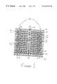
- FIG. 1is a top view of a multichip package as taken from beneath a top layer of encapsulating material according to one embodiment of the present invention
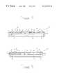
- FIG. 2is a cross section view of the multichip package of FIG. 1 taken along line 2 — 2 ;
- FIG. 3is a cross section view of a multichip package having conductive leads extending beyond the encapsulating compound according to another embodiment of the present invention
- FIG. 4is a cross section view of a multichip package having conductive leads sheared flush with the encapsulating compound according to a further embodiment of the present invention.
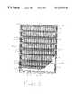
- FIG. 5is a top perspective view of a multichip package with a cut-away view through the encapsulating material to reveal eight semiconductor chips and a plurality of common busses across the semiconductor chips according to a still further embodiment of the present invention.
- the present inventionrelates to a novel multichip semiconductor package having a plurality of semiconductor chips fabricated as a singular coextensive substrate and to its method of making.
- a multichip semiconductor packagedepicted generally as package 20 , has a plurality of semiconductor chips 22 each arranged in electrical isolation, one from another, adjacently along a terminal boundary 24 thereof as a singular coextensive substrate 26 .
- Chips 22are integrally formed on substrate 26 which may be a semiconductor material such as gallium arsenide, silicon, or can be silicon on sapphire, silicon on insulator.
- substrate 26preferably a monocrystalline silicon wafer, has the individual semiconductor chips 22 fabricated thereon by conventional techniques currently employed in the manufacture of single-chip packages.
- a lead frame 28attached to semiconductor chip 22 , preferably by lamination techniques using a lead-over-chip (LOC) adhesive 27 , a lead locking tape 29 , and a wire bonding segment 31 , is a lead frame 28 to which electrodes 30 are electrically contacted.
- Lead frame 28is provided, one per package 20 , to yield electrical continuity between electrodes 30 and the internal devices of semiconductor chip 22 by way of a singular conductive lead 32 , one per each electrode 30 .
- Electrode 30is connected to conductive lead 32 at a selected position along a length thereof. It should be appreciated that each selected position of connection between each electrode 30 and each respective conductive lead 32 yields an arrangement of electrodes 30 about package 20 , known commonly as a package footprint.
- the package footprinthas a corresponding footprint on a PWB (not shown), for example, that allows for completion of an electrical circuit between the internal devices of package 20 and the circuit fabricated on the PWB when the two footprints are electrically connected.
- each electrode 30is not directly connected to semiconductor chip 22 by way of bond pads or wiring traces, as are conventional BGA's , flip-chips, and chip-scale packages, the package footprint can remain consistent in size and shape despite continual size reductions in individual semiconductor chips. This is possible because the length of conductive lead 32 acts as an electrical bus from the internal devices in semiconductor chips 22 to the position of electrode 30 . As semiconductor chip 22 is reduced in size, the dimensions of conductive lead 32 are adjusted and electrical continuity remains bussed out to electrode 30 .
- conductive leads 32are plated at an electrode bond area 58 with a thin layer of metal to improve the strength and conductivity between electrode 30 and conductive lead 32 .
- electrodes 30can be solder balls, the metal composition thereof is preferably gold, palladium/nickel, or tin.
- the package footprinthas rows 35 of electrodes 30 disposed across semiconductor chips 22 in two substantially parallel lines 34 , 36 with each individual electrode 30 being contacted, one per each conductive lead 32 , along an extended portion 38 of the substantially rectangular conductive lead.
- the extended portionis present on conductive lead 32 because the width of the remainder of conductive lead 32 , while a cost effective use of materials, is too thin to fully accommodate electrode 30 .
- electrode 30only exceeds the width of conductive leads 32 to the extent necessary to prevent mechanical bonding failures, such as solder joint failures.
- Conductive leads 32are preferably arranged in sets of pairs 40 , 42 across semiconductor chips 22 . Each pair set 40 , 42 is arranged in relatively close proximity. Each extended portion 38 of each conductive lead 32 is staggered with respect to another extended portion 38 of conductive lead 32 in the same or juxtaposed to pair set 4 O, 42 . In this manner, multiple electrodes 30 are available for close proximity positioning while, simultaneously, avoiding electrical shorts in and amongst pair sets 40 , 42 which would otherwise occur with electrodes of the size and shape depicted if electrodes 30 were all placed side-by-side in a linear fashion.
- electrode 30changes in the size and shape of electrode 30 are contemplated that would yield other distinct package footprints without altering the fabrication or effectiveness of singular coextensive substrate 26 having a plurality of semiconductor chips 22 integrally formed thereon.
- the portion of electrode 30 contacting conductive lead 32can be reduced in area to a size that does not exceed the pitch of conductive leads 32 , thereby making extended portions 38 superfluous.
- extended portions 38could be alternated at opposite ends of their respective pair sets 40 , 42 or arranged in other ways that maintain a cost effective conductive lead 32 while preventing electrical shorts.
- the plurality of semiconductor chips 22are electrically bonded together, along a periphery 43 and a central portion 44 of package 20 , by way of bond pads 45 and bond wires 46 to form, for example, a larger package circuit, or as in a preferred embodiment, to expand the overall memory of semiconductor chips, such as DRAM semiconductor chips.
- the bond padscan be any of the various terminals formed near the surface of semiconductor chip 22 through which electrical connections can be made between the active devices in chip 22 and external circuits.
- Bond wires 46are preferably connected along a terminal end 48 of conductive leads 32 at a wire bond area as depicted in FIGS. 3 and 4.
- conductive leads 32are plated at wire bond area 56 with a thin layer of metal suitable for wire bonding, such as gold, silver or palladium/nickel to improve the strength and conductivity of the bond between conductive leads 32 and bond wires 46 .
- Package 20is encapsulated in a compound 50 which has openings formed therein that partially expose conductive leads 32 at the selected connection positions, which is preferably electrode bond area 58 .
- the openingsare sized and shaped according to the selected size and shape of electrodes 30 and are adjustable to correspond with changes in the selected size and shape.
- Compound 50often a molding compound, is generally an electrically insulating formulation used to distribute power, dissipate heat and protect the active devices therein from thermomechanical stresses and pollutants found in the operating environment.
- compound 50is a thermosetting epoxy resin, but may also be silicon, phenolic, or polyeurethane.
- the composition of compound 50is generally derived from a balance of numerous engineering factors including the cost of manufacturing, production volume, expected use environment, expected use market and other related considerations. It is also contemplated that compound 50 may be a polyimide compound useful as an alpha barrier.
- conductive leads 32have been fully encapsulated within compound 50 .
- conductive leads 32are extended out from compound 50 to facilitate chip testing and also to enable package 20 to be easily maneuvered during the manufacturing process. It is also contemplated that conductive leads 32 could remain attached to semiconductor chips 22 without any of, or as a compliment to, electrodes 30 so that a signal could be taken directly therefrom as package 20 is used in either a surface mount, or through-hole capacity.
- conductive leads 32have been sheared flush with compound 50 after either testing or manufacturing in order to create a thicker and stronger terminal portion of package 20 , or to remove any potential mechanical interferences from conductive leads 32 .
- package 20has eight semiconductor chips 22 adjacently arranged in electrical isolation, in the manner previously described, with conductive leads 32 again disposed in pairs 40 , 42 across substrate 26 .
- conductive leads 32 in this embodimentare bussed common to eliminate high wiring density within package 20 and to provide for redundant back-up in the event a semiconductor chip 22 has a bad, or deteriorated, signal line.
- the common bussingalso allows for common addresses (AO, Al . . . An), common data out (DO), common data queries (DQ) or voltage steady state (Vss) electrodes, for example, to be fabricated together electrically, thereby eliminating electrode repetition and reducing material costs.
- a plurality of wiring banks 54are configured about the periphery of package 20 along three sides and about the interior of package 20 in rows 35 having two substantially parallel lines 34 , 36 of electrodes 30 . It should be understood that wiring banks 54 could all be grouped together, but to do so would be at the expense of increasing wiring densities and creating manufacturing difficulties such as having inadequate wiring angles for attaching bond pads 45 to conductive leads 32 . Yet, alternatives exist that will effectively accommodate the grouping of wiring banks 54 about package 20 that provide ease of electrical connection with other external circuits and are within the spirit of the present invention.
- this embodimentdepicts compound 50 as being disposed upon top side 60 of substrate 26 while bottom side 62 remains uncovered. It is possible, however, to forego disposing any of compound 50 on substrate 26 . It is preferred, however, that at least a partial encapsulation of compound 50 is applied about substrate 26 to prevent undesirable conditions, such as electrical shorting.
- semiconductor chips 22have heretofore been described as either being two or eight in number and fabricated in adjacent arrangement with one another within substantially rectangular packages, one skilled in the art should appreciate that still other embodiments exist that are within the express teachings of the present invention.
- semiconductor chips 22range in preferred quantities from 2 to 8 but may also be as large as 64 or more.
- the arrangement of semiconductor chips 22may also be fabricated into various other patterns so long as chips 22 remain as discrete, electrically isolated units integrally formed on singular coextensive substrate 26 .
- the steps of fabrication of multichip package 20include a singular substrate 26 being fabricated with a plurality of electrically isolated semiconductor chips 22 thereon. Instead of a singulation process of sawing the individual chips into discrete single-chips for packaging, chips 22 are kept as integrally form electrically isolated elements that are there after electrically connected together.
- bond pads 45are provided to connect to the active devices (not shown) by exposing bond pads 45 through apertures in an insulating or passivation layer which forms the upper surface of chip 22 .
- Conductive leads 32which form the inner portion of the singular lead frame 28 , are then positioned over chips 22 and extended in length to an area near bond pads 45 for wire bonding connections thereto.
- Conductive leads 32are usually prefabricated with a plating of a thin layer of suitable metal at terminal end 48 but can also be plated after encapsulation. In sequence, conductive leads 32 are connected to an upper surface of chips 22 with LOC adhesive 27 .
- LOC adhesive 27For a detailed description thereof, refer to U.S. Pat. No. 5,286,679, issued to Farnsworth et al., which is incorporated herein by reference.
- package 20is at least partially encapsulated with compound 50 and openings are formed therein to at least partially expose conductive leads 32 , where exposure preferably is at electrode bond area 58 .
- conductive leads 32are usually prefabricated with a plating of a thin layer of suitable metal at electrode bond area 58 . After encapsulation, any remaining resin residue that is present on the wire or electrode bond area 46 , 58 is removed by electrolytic or mechanical deflash processes known in the art.
Landscapes
- Engineering & Computer Science (AREA)
- Microelectronics & Electronic Packaging (AREA)
- Power Engineering (AREA)
- Physics & Mathematics (AREA)
- Condensed Matter Physics & Semiconductors (AREA)
- General Physics & Mathematics (AREA)
- Computer Hardware Design (AREA)
- Wire Bonding (AREA)
- Semiconductor Integrated Circuits (AREA)
Abstract
Description
1. The Field of the Invention
The present invention relates generally to multichip semiconductor packages and particularly relates to an improved semiconductor package having a plurality of semiconductor chips fabricated as a singular coextensive substrate and to its method of making.
2. The Relevant Technology
Multichip packaging is one of the fastest growing disciplines in the chip packaging industry. Initially, the multichip package came into existence for applications requiring numerous and varied circuits configured into a least amount of space, such as with mainframes and supercomputers. Since then, multichip packages have transcended traditional boundaries and moved into conventional single-chip applications because they characteristically possess reduced weight and size per each circuit, increased reliability and increased electrical performance. As such, multichip packages are now regularly employed in consumer electronics, medical and avionic devices, and in the automotive and aerospace industries. Multichip packages also find particular usefulness in telecommunication applications because of their high bandwidth performance.
In general, conventional multichip packages are available in one of two varieties. One has two or more bare chips bonded directly to a multichip substrate and the other, the most commercially predominant package, having two or more pre-packaged single-chips, in their respective single-chip carriers and bonded to a multichip substrate. Although the former variety enjoys advantages over the latter, both varieties remain bound by single-chip constraints because of their dependence upon either a bare, or packaged, single-chip. As such, both varieties frequently share common problems with their single-chip counterparts.
For example, in response to an industry-wide demand for high lead counts and small “footprints,” i.e., the arrangement of electrical contacts on the printed circuit board to which the chip package is ultimately connected, single-chip packages became available in Ball Grid Array (BGA), “flip-chip” and “chip-scale” packages. The problem, however, is that these singular-chip packages have external electrodes, which can be solder balls, that are directly attached to contacts on the surface of the semiconductor chip. As semiconductor chips are continually reduced in size, the arrangement of the external electrodes must also be continually reconfigured into a correspondingly smaller size. In turn, the footprint on the printed circuit board must also be continually reconfigured. This problem is even further amplified with multichip packages because footprint reconfiguration also needs to occur on the multichip substrate itself to which the single-chip packages are attached. It is, therefore, desirous to eliminate the continual reconfiguring of the footprint of the multichip package and the rearrangement of the multichip substrate.
In a separate and distinct discipline, Wafer Scale Integration (WSI) techniques have been used to fabricate various other multichip arrangements. Yet WSI often utilizes 800, or more, semiconductor chips as a single multichip which, in effect, is too cumbersome, if not prohibitive, to encapsulate into a package format. The large size is also inefficient for applications requiring relatively few semiconductor chips, around 64 or less, because of the high wiring density used in WSI wirebonding operations and the surplus unneeded chips. Effective testing of each individual chip with WSI is also problematic because of the large number of chips. Additionally, WSI techniques frequently require expensive photolithography equipment, not typically utilized with single-chip packages, to transfer a circuit image onto a multichip substrate.
A need exists for a multichip package that overcomes the foregoing problems.
In accordance with the invention as embodied and broadly described herein, a novel multichip semiconductor package, and method of making, is provided that has a plurality of semiconductor chips fabricated in electrical isolation, one from another, as a singular coextensive semiconductor substrate useful for numerous and varied semiconductor chip applications. In the context of this document, the term “semiconductor substrate” is defined to mean any construction comprising semiconductive material, including but not limited to bulk semiconductive material such as a semiconductive wafer, either alone or in assemblies comprising other materials thereon, and semiconductive material layers, either alone or in assemblies comprising other materials. The term “substrate” refers to any supporting structure including but not limited to the semiconductor substrates described above. As such, silicon on insulator and silicon on sapphire are within the definition of substrate.
Once fabricated, instead of being singulated into a plurality of single-chip packages, the semiconductor chips are kept integrally on the substrate. The semiconductor chips, which are electrically isolated one from another, are then wired so as to be electrically connected together to form a larger circuit, such as to expand a memory circuit, and then encapsulated and processed into a single, multichip package.
In a preferred embodiment, a multichip package has a plurality of electrically isolated semiconductor chips integrally formed on a unitary semiconductor substrate. A plurality of conductive leads electrically connect the electrically isolated semiconductor chips. A compound substantially encapsulates at least a portion of the semiconductor substrate, and a plurality of electrodes extend through the compound to make contact with the conductive leads.
In another preferred embodiment, a multichip semiconductor package includes a plurality of electrically isolated semiconductor chips that are integrally formed on a unitary semiconductor substrate, each semiconductor chip having an active device formed thereon. The multichip semiconductor package also includes a plurality of bond pads, each bond pad being electrically connected one per each active device. A plurality of conductive leads electrically connect the electrically isolated semiconductor chips, where each conductive lead is electrically connected one per each bond pad. A compound substantially encapsulates at least a portion of the semiconductor substrate, the bond pads, and the conductive leads. There are also a plurality of solder balls, where each solder ball extends through the compound to make contact with a respective one of the conductive leads.
In yet another preferred embodiment, the common signals of the plurality of semiconductor chips are bussed in electrical common across the substrate to a common electrode suitable for electrically providing the signal to another, external circuit, such as a Printed Wiring Board (PWB). The common bussing is achieved by conductive leads disposed across the substrate in pair sets having an extended portion that accommodates the electrode in contact therewith. The electrode contacts the conductive lead through an opening formed in the encapsulant that surrounds the substrate. The extended portions of each conductive lead are staggered with respect to the extended portion of the conductive lead in the same, or juxtaposed, pair set. In this manner, multiple electrodes are available for close proximity positioning while, simultaneously, avoiding electrical shorts amongst the pair sets.
In an alternate embodiment, the conductive leads extend beyond the encapsulant to facilitate testing or improve manageability of the package during the manufacturing process. The conductive leads, after the testing or manufacturing, may then be sheared flush to avoid mechanical interferences between the external circuit, i.e., the PWB, or to create a stronger and thicker multichip package.
A method of making the inventive multichip package includes providing a unitary semiconductor substrate and integrally forming a plurality of electrically isolated semiconductor chips on the unitary semiconductor substrate. There is then formed a plurality of conductive leads that electrically connect the electrically isolated semiconductor chips. A compound then substantially encapsulates at least a portion of the semiconductor substrate, and a plurality of electrodes are formed so as to extend through the compound to make contact with the conductive leads.
Another method of making the inventive multichip package includes providing a unitary semiconductor substrate. A plurality of electrically isolated semiconductor chips are integrally formed on the unitary semiconductor substrate each having an active device formed thereon. A plurality of bond pads are formed so as to make electrical connections from each bond pad to one of the active devices. Electrical connections are also formed to electrically connect the electrically isolated semiconductor chips with a plurality of conductive leads. Each conductive lead is electrically connected one per each bond pad. A compound is formed so as to substantially encapsulate at least a portion of the semiconductor substrate, the bond pads, and the conductive leads. A plurality of solder balls are formed so as to extend through the compound to make contact with a respective one of the conductive leads.
A still further method of making the inventive multichip package includes a singular substrate being fabricated with a plurality of electrically isolated semiconductor chips integrally formed thereon. Centrally located bond pads are provided for connection with the active devices of the chips by exposing the bond pads through apertures in an insulating or passivation layer which forms the upper surface of each chip. Conductive leads are positioned over the chips and are extended in length to an area near the bond pads for wire bonding connections thereto. The conductive leads are attached to an upper surface of the chips with Lead-Over-Chip (LOC) tape. The multichip package is at least partially encapsulated with a compound, and openings are formed in the compound to at least partially expose the conductive leads. Electrodes are made to contact the conductive leads that are exposed through the openings in the compound.
These and other features of the present invention will become more fully apparent from the following description and appended claims, or may be learned by the practice of the invention as set forth hereinafter.
In order to more fully understand the manner in which the above-recited and other advantages of the invention are obtained, a more particular description of the invention will be rendered by reference to the specific embodiments thereof which are illustrated in the appended drawings. Understanding that these drawings depict only typical embodiments of the invention and are not therefore to be considered to be limiting of its scope, the invention in its presently understood best mode for making and using the same will be described and explained with additional specificity and detail through the use of the accompanying drawings in which:
FIG. 1 is a top view of a multichip package as taken from beneath a top layer of encapsulating material according to one embodiment of the present invention;
FIG. 2 is a cross section view of the multichip package of FIG. 1 taken along line2—2;
FIG. 3 is a cross section view of a multichip package having conductive leads extending beyond the encapsulating compound according to another embodiment of the present invention;
FIG. 4 is a cross section view of a multichip package having conductive leads sheared flush with the encapsulating compound according to a further embodiment of the present invention; and
FIG. 5 is a top perspective view of a multichip package with a cut-away view through the encapsulating material to reveal eight semiconductor chips and a plurality of common busses across the semiconductor chips according to a still further embodiment of the present invention.
The present invention relates to a novel multichip semiconductor package having a plurality of semiconductor chips fabricated as a singular coextensive substrate and to its method of making.
With reference to FIGS. 1 and 2, a multichip semiconductor package, depicted generally aspackage 20, has a plurality ofsemiconductor chips 22 each arranged in electrical isolation, one from another, adjacently along aterminal boundary 24 thereof as a singularcoextensive substrate 26.Chips 22 are integrally formed onsubstrate 26 which may be a semiconductor material such as gallium arsenide, silicon, or can be silicon on sapphire, silicon on insulator.Substrate 26, preferably a monocrystalline silicon wafer, has theindividual semiconductor chips 22 fabricated thereon by conventional techniques currently employed in the manufacture of single-chip packages. The difference, however, is that instead of dividingindividual chips 22 into discrete single-chip packages by a singulation process performed upon the wafer, the individual chips, though electrically isolated one from another, and then electrically connected are then encapsulated into asingular multichip package 20 as described hereinafter.
In particular, attached tosemiconductor chip 22, preferably by lamination techniques using a lead-over-chip (LOC) adhesive27, alead locking tape 29, and awire bonding segment 31, is alead frame 28 to whichelectrodes 30 are electrically contacted.Lead frame 28 is provided, one perpackage 20, to yield electrical continuity betweenelectrodes 30 and the internal devices ofsemiconductor chip 22 by way of a singularconductive lead 32, one per eachelectrode 30.Electrode 30 is connected toconductive lead 32 at a selected position along a length thereof. It should be appreciated that each selected position of connection between eachelectrode 30 and each respectiveconductive lead 32 yields an arrangement ofelectrodes 30 aboutpackage 20, known commonly as a package footprint. The package footprint has a corresponding footprint on a PWB (not shown), for example, that allows for completion of an electrical circuit between the internal devices ofpackage 20 and the circuit fabricated on the PWB when the two footprints are electrically connected. Advantageously, since eachelectrode 30 is not directly connected tosemiconductor chip 22 by way of bond pads or wiring traces, as are conventional BGA's , flip-chips, and chip-scale packages, the package footprint can remain consistent in size and shape despite continual size reductions in individual semiconductor chips. This is possible because the length ofconductive lead 32 acts as an electrical bus from the internal devices insemiconductor chips 22 to the position ofelectrode 30. Assemiconductor chip 22 is reduced in size, the dimensions ofconductive lead 32 are adjusted and electrical continuity remains bussed out toelectrode 30. Typically, as in FIGS. 3 and 4, conductive leads32 are plated at anelectrode bond area 58 with a thin layer of metal to improve the strength and conductivity betweenelectrode 30 andconductive lead 32. Sinceelectrodes 30 can be solder balls, the metal composition thereof is preferably gold, palladium/nickel, or tin.
In the preferred embodiment of FIG. 1, the package footprint hasrows 35 ofelectrodes 30 disposed acrosssemiconductor chips 22 in two substantiallyparallel lines individual electrode 30 being contacted, one per eachconductive lead 32, along anextended portion 38 of the substantially rectangular conductive lead. The extended portion is present onconductive lead 32 because the width of the remainder ofconductive lead 32, while a cost effective use of materials, is too thin to fully accommodateelectrode 30. It should be appreciated thatelectrode 30 only exceeds the width of conductive leads32 to the extent necessary to prevent mechanical bonding failures, such as solder joint failures.
Conductive leads32 are preferably arranged in sets ofpairs semiconductor chips 22. Each pair set40,42 is arranged in relatively close proximity. Eachextended portion 38 of eachconductive lead 32 is staggered with respect to another extendedportion 38 ofconductive lead 32 in the same or juxtaposed to pair set4O,42. In this manner,multiple electrodes 30 are available for close proximity positioning while, simultaneously, avoiding electrical shorts in and amongst pair sets40,42 which would otherwise occur with electrodes of the size and shape depicted ifelectrodes 30 were all placed side-by-side in a linear fashion. Yet, it should be appreciated that changes in the size and shape ofelectrode 30 are contemplated that would yield other distinct package footprints without altering the fabrication or effectiveness of singularcoextensive substrate 26 having a plurality ofsemiconductor chips 22 integrally formed thereon. For example, it is contemplated that the portion ofelectrode 30 contactingconductive lead 32 can be reduced in area to a size that does not exceed the pitch of conductive leads32, thereby makingextended portions 38 superfluous. It is also contemplated thatextended portions 38 could be alternated at opposite ends of their respective pair sets40,42 or arranged in other ways that maintain a cost effectiveconductive lead 32 while preventing electrical shorts.
The plurality ofsemiconductor chips 22 are electrically bonded together, along aperiphery 43 and acentral portion 44 ofpackage 20, by way ofbond pads 45 andbond wires 46 to form, for example, a larger package circuit, or as in a preferred embodiment, to expand the overall memory of semiconductor chips, such as DRAM semiconductor chips. It is to be appreciated that the bond pads can be any of the various terminals formed near the surface ofsemiconductor chip 22 through which electrical connections can be made between the active devices inchip 22 and external circuits.Bond wires 46 are preferably connected along aterminal end 48 of conductive leads32 at a wire bond area as depicted in FIGS. 3 and 4. Typically, conductive leads32 are plated at wire bond area56 with a thin layer of metal suitable for wire bonding, such as gold, silver or palladium/nickel to improve the strength and conductivity of the bond between conductive leads32 andbond wires 46.
In the preferred embodiment depicted in FIG. 2, conductive leads32 have been fully encapsulated withincompound 50. There are other useful embodiments for conductive leads32. For example, in FIG. 3, conductive leads32 are extended out fromcompound 50 to facilitate chip testing and also to enablepackage 20 to be easily maneuvered during the manufacturing process. It is also contemplated that conductive leads32 could remain attached tosemiconductor chips 22 without any of, or as a compliment to,electrodes 30 so that a signal could be taken directly therefrom aspackage 20 is used in either a surface mount, or through-hole capacity. In FIG. 4, conductive leads32 have been sheared flush withcompound 50 after either testing or manufacturing in order to create a thicker and stronger terminal portion ofpackage 20, or to remove any potential mechanical interferences from conductive leads32.
With reference to FIG. 5,package 20 has eightsemiconductor chips 22 adjacently arranged in electrical isolation, in the manner previously described, withconductive leads 32 again disposed inpairs substrate 26. Instead of the semiconductor chips22 being interconnected by discretely wiring conductive leads32 thereof, conductive leads32 in this embodiment are bussed common to eliminate high wiring density withinpackage 20 and to provide for redundant back-up in the event asemiconductor chip 22 has a bad, or deteriorated, signal line. The common bussing also allows for common addresses (AO, Al . . . An), common data out (DO), common data queries (DQ) or voltage steady state (Vss) electrodes, for example, to be fabricated together electrically, thereby eliminating electrode repetition and reducing material costs. Although some signal lines are independent and cannot, for various reasons, be bussed common, such as individual chip enables (CE) and row address strobes (RAS), those signal lines can be grouped together into common areas for efficaciously facilitating interconnection with an external circuit, such as a PWB. For example, a plurality ofwiring banks 54 are configured about the periphery ofpackage 20 along three sides and about the interior ofpackage 20 inrows 35 having two substantiallyparallel lines electrodes 30. It should be understood that wiringbanks 54 could all be grouped together, but to do so would be at the expense of increasing wiring densities and creating manufacturing difficulties such as having inadequate wiring angles for attachingbond pads 45 to conductive leads32. Yet, alternatives exist that will effectively accommodate the grouping ofwiring banks 54 aboutpackage 20 that provide ease of electrical connection with other external circuits and are within the spirit of the present invention.
In response to industry demands for thin packages, this embodiment depictscompound 50 as being disposed upontop side 60 ofsubstrate 26 whilebottom side 62 remains uncovered. It is possible, however, to forego disposing any ofcompound 50 onsubstrate 26. It is preferred, however, that at least a partial encapsulation ofcompound 50 is applied aboutsubstrate 26 to prevent undesirable conditions, such as electrical shorting.
Although the arrangement of the discrete electricallyisolated semiconductor chips 22 has heretofore been described as either being two or eight in number and fabricated in adjacent arrangement with one another within substantially rectangular packages, one skilled in the art should appreciate that still other embodiments exist that are within the express teachings of the present invention. For example, it is contemplated that semiconductor chips22 range in preferred quantities from 2 to 8 but may also be as large as 64 or more. The arrangement ofsemiconductor chips 22 may also be fabricated into various other patterns so long aschips 22 remain as discrete, electrically isolated units integrally formed on singularcoextensive substrate 26.
The steps of fabrication ofmultichip package 20 include asingular substrate 26 being fabricated with a plurality of electricallyisolated semiconductor chips 22 thereon. Instead of a singulation process of sawing the individual chips into discrete single-chips for packaging, chips22 are kept as integrally form electrically isolated elements that are there after electrically connected together. Next,bond pads 45 are provided to connect to the active devices (not shown) by exposingbond pads 45 through apertures in an insulating or passivation layer which forms the upper surface ofchip 22.
Conductive leads32, which form the inner portion of thesingular lead frame 28, are then positioned overchips 22 and extended in length to an area nearbond pads 45 for wire bonding connections thereto. Conductive leads32 are usually prefabricated with a plating of a thin layer of suitable metal atterminal end 48 but can also be plated after encapsulation. In sequence, conductive leads32 are connected to an upper surface ofchips 22 withLOC adhesive 27. For a detailed description thereof, refer to U.S. Pat. No. 5,286,679, issued to Farnsworth et al., which is incorporated herein by reference.
Once connected,package 20 is at least partially encapsulated withcompound 50 and openings are formed therein to at least partially exposeconductive leads 32, where exposure preferably is atelectrode bond area 58. Also, conductive leads32 are usually prefabricated with a plating of a thin layer of suitable metal atelectrode bond area 58. After encapsulation, any remaining resin residue that is present on the wire orelectrode bond area
Lastly,electrodes 30, preferably solder balls, are bonded toelectrode bond areas 58 through openings incompound 50. The solder balls may be attached, as is known in the art, by coating the solder balls orbond areas 58 with flux, placing the solder balls onelectrode bond area 58 through openings with conventional pick and place or shaker/hopper equipment, and reflowing the balls in place using an infrared or hot air reflow process. The excess flux is then removed with an appropriate cleaning agent. In this manner, the solder balls are electrically and mechanically connected toconductive leads 32 to formelectrodes 30 external to compound50. Other processes may also be used to formelectrodes 30. For example,electrodes 30 may be “plated up” using conventional plating techniques rather than using the solder ball techniques as described above. The completedmultichip semiconductor package 20 can then be assembled to a printed circuit board or the like using conventional surface mount or through hole processes and equipment.
While there has been shown and described a novel multichip package having a package footprint configured independently of the size of the individual semiconductor chips therein that is made with conventional leaded chip packaging processes and equipment, it is to be appreciated that the present invention may be embodied in other specific forms without departing from its spirit or essential characteristics. The described embodiments are to be considered, in all respects, only as illustrative and not restrictive. The scope of the invention is, therefore, indicated by the appended claims rather than by the foregoing description. All changes which come within the meaning and range of equivalency of the claims are to be embraced within their scope.
Claims (19)
1. A multichip package, comprising:
a plurality of electrically isolated semiconductor chips situated upon a semiconductor substrate that is a unitary, separated piece of a semiconductor wafer;
a plurality of conductive leads, not integrally fabricated into the semiconductor substrate, that electrically connect the electrically isolated semiconductor chips on the semiconductor substrate;
a compound encapsulating at least a portion of the semiconductor substrate; and
a plurality of solder balls for electrically communicating with the semiconductor chips through said compound;
wherein each conductive lead has an extended portion of increased surface area on one side thereof that makes contact with a solder ball of the plurality of solder balls and has a linear portion with no extended portion on an opposite side thereof that faces a linear portion of an adjacent conductive lead.
2. A multichip package according toclaim 1 , wherein said solder balls project from the semiconductor chips to extend above said compound.
3. A multichip package according toclaim 2 , wherein said solder balls are arranged linearly across said semiconductor substrate in at least two lines.
4. A multichip package according toclaim 3 , wherein said plurality of conductive leads provide electrical communication between said solder balls and said semiconductor chips.
5. A multichip package according toclaim 1 , wherein:
the plurality of electrically isolated semiconductor chips comprise a linear series of adjacent chips; and
the plurality of conductive leads run substantially parallel to the linear series of adjacent chips and electrically connect each chip to each adjacent chip.
6. A multichip semiconductor package, comprising:
a plurality of electrically isolated semiconductor chips situated upon a semiconductor substrate that is a unitary, separated piece of a semiconductor wafer, each semiconductor chip having an active device formed thereon;
a plurality of bond pads, each bond pad being electrically connected one per each said active device;
a plurality of conductive leads, not integrally fabricated into the semiconductor substrate, that electrically connect the electrically isolated semiconductor chips, each conductive lead being electrically connected one per each bond pad;
a compound encapsulating at least a portion of the semiconductor substrate, said bond pads, and said conductive leads; and
a plurality of solder balls each extending through said compound to make contact with a respective one of said conductive leads;
wherein each conductive lead has an extended portion of increased surface area on one side thereof that makes contact with a solder ball of the plurality of solder balls and has a linear portion with no extended portion on an opposite side thereof that faces a linear portion of an adjacent conductive lead.
7. A multichip package according toclaim 6 , wherein said conductive leads are disposed in pairs across said semiconductor substrate.
8. A multichip package according toclaim 7 , wherein each pair of conductive leads has two extended portions of increased surface area to accommodate two solder balls of said plurality of solder balls.
9. A multichip package, comprising:
a plurality of electrically isolated semiconductor chips situated upon a semiconductor substrate that is a unitary, separated piece of a semiconductor wafer;
a compound encapsulating at least a portion of said semiconductor substrate;
a plurality of electrodes, not integrally fabricated into the unitary, separated piece of the semiconductor wafer, in electrical communication with at least one of said plurality of semiconductor chips through said compound; and
a plurality of conductive leads, not integrally fabricated into the unitary, separated piece of the semiconductor wafer;
wherein each conductive lead is positioned over the semiconductor substrate and has an extended portion of increased surface area on one side thereof that makes contact with an electrode of said plurality of electrodes and has a linear portion with no extended portion on an opposite side thereof that faces a linear portion of an adjacent conductive lead.
10. A multichip package according toclaim 9 , wherein said conductive lead has an electrode bond area for contacting with said electrode.
11. A multichip package according toclaim 9 , further comprising a wiring bank extending about a periphery of said semiconductor substrate.
12. A multichip package according toclaim 11 wherein said semiconductor substrate further comprises a plurality of wiring banks extending about said periphery and arranged in a plurality of at least two parallel rows.
13. A multichip package according toclaim 9 , wherein said compound encapsulates all of said semiconductor substrate.
14. The multichip package according toclaim 9 , wherein the number of said electrically isolated semiconductor chips on the unitary, separated piece of the semiconductor wafer is not greater than 64.
15. The multichip package according toclaim 9 , wherein the number of said electrically isolated semiconductor chips on the unitary, separated piece of the semiconductor wafer is from 2 to 8.
16. A multichip package, comprising:
a plurality of electrically isolated semiconductor chips in a unitary, separated piece of a semiconductor wafer, each said chip having an electrical device therein;
a compound encapsulating at least a portion of said unitary, separated piece;
a plurality of electrodes, not integrally fabricated into the unitary, separated piece of the semiconductor wafer, in electrical communication with at least one of said plurality of semiconductor chips through said compound;
a plurality of conductive leads, not integrally fabricated into the unitary, separated piece of the semiconductor wafer, electrically connecting between said electrodes and said at least one of said electrically isolated semiconductor chips;
a plurality of electrical connections each being in electrical communication with one said electrical device of one of said semiconductor chips; and
electrical wiring upon the unitary, separated piece of the semiconductor wafer, not integrally fabricated into the unitary, separated piece of the semiconductor wafer, in electrical communication with said plurality of electrical connections so as to place said electrically isolated semiconductor chips on the unitary, separated piece of the semiconductor wafer in electrical communication one with another;
wherein each conductive lead is positioned over the semiconductor substrate and has an extended portion of increased surface area on one side thereof that makes contact with an electrode of said plurality of electrodes and has a linear portion with no extended portion on an opposite side thereof that faces a linear portion of an adjacent conductive lead.
17. The multichip package according toclaim 16 , wherein:
said conductive leads comprise a plurality of parallel conductive leads; and
each said conductive lead has thereon a solder ball.
18. The multichip package according toclaim 17 , wherein said plurality of parallel conductive leads comprise consecutive first, second, third, and fourth leads, wherein the geometric centers of the respective solder balls on the first and third leads form a line that is:
perpendicular to said plurality of parallel conductive leads; and
parallel to a line that is formed by the geometric centers of the respective solder balls on the second and fourth leads.
19. The multichip package according toclaim 18 , wherein:
a tangent to the periphery of the solder ball on the second lead intersects the solder ball on the third lead; and
said tangent is parallel to said plurality of parallel conductive leads and is taken at a point on the solder ball on the second lead that is closest to the third lead.
Priority Applications (6)
| Application Number | Priority Date | Filing Date | Title |
|---|---|---|---|
| US09/032,191US6429528B1 (en) | 1998-02-27 | 1998-02-27 | Multichip semiconductor package |
| AU26861/99AAU2686199A (en) | 1998-02-27 | 1999-02-18 | Multichip semiconductor package and method of making |
| PCT/US1999/003493WO1999044235A1 (en) | 1998-02-27 | 1999-02-18 | Multichip semiconductor package and method of making |
| US09/502,538US6228548B1 (en) | 1998-02-27 | 2000-02-11 | Method of making a multichip semiconductor package |
| US10/153,086US6906409B2 (en) | 1998-02-27 | 2002-05-22 | Multichip semiconductor package |
| US11/138,169US20050212143A1 (en) | 1998-02-27 | 2005-05-26 | Multichip semiconductor package |
Applications Claiming Priority (1)
| Application Number | Priority Date | Filing Date | Title |
|---|---|---|---|
| US09/032,191US6429528B1 (en) | 1998-02-27 | 1998-02-27 | Multichip semiconductor package |
Related Child Applications (2)
| Application Number | Title | Priority Date | Filing Date |
|---|---|---|---|
| US09/502,538DivisionUS6228548B1 (en) | 1998-02-27 | 2000-02-11 | Method of making a multichip semiconductor package |
| US10/153,086ContinuationUS6906409B2 (en) | 1998-02-27 | 2002-05-22 | Multichip semiconductor package |
Publications (2)
| Publication Number | Publication Date |
|---|---|
| US20020053743A1 US20020053743A1 (en) | 2002-05-09 |
| US6429528B1true US6429528B1 (en) | 2002-08-06 |
Family
ID=21863595
Family Applications (4)
| Application Number | Title | Priority Date | Filing Date |
|---|---|---|---|
| US09/032,191Expired - LifetimeUS6429528B1 (en) | 1998-02-27 | 1998-02-27 | Multichip semiconductor package |
| US09/502,538Expired - LifetimeUS6228548B1 (en) | 1998-02-27 | 2000-02-11 | Method of making a multichip semiconductor package |
| US10/153,086Expired - LifetimeUS6906409B2 (en) | 1998-02-27 | 2002-05-22 | Multichip semiconductor package |
| US11/138,169AbandonedUS20050212143A1 (en) | 1998-02-27 | 2005-05-26 | Multichip semiconductor package |
Family Applications After (3)
| Application Number | Title | Priority Date | Filing Date |
|---|---|---|---|
| US09/502,538Expired - LifetimeUS6228548B1 (en) | 1998-02-27 | 2000-02-11 | Method of making a multichip semiconductor package |
| US10/153,086Expired - LifetimeUS6906409B2 (en) | 1998-02-27 | 2002-05-22 | Multichip semiconductor package |
| US11/138,169AbandonedUS20050212143A1 (en) | 1998-02-27 | 2005-05-26 | Multichip semiconductor package |
Country Status (3)
| Country | Link |
|---|---|
| US (4) | US6429528B1 (en) |
| AU (1) | AU2686199A (en) |
| WO (1) | WO1999044235A1 (en) |
Cited By (48)
| Publication number | Priority date | Publication date | Assignee | Title |
|---|---|---|---|---|
| US20030038352A1 (en)* | 2001-08-22 | 2003-02-27 | Christian Hauser | Electronic component with a semiconductor chip and fabrication method |
| US20030042581A1 (en)* | 2001-08-29 | 2003-03-06 | Fee Setho Sing | Packaged microelectronic devices and methods of forming same |
| US20030104654A1 (en)* | 2000-06-28 | 2003-06-05 | Farnworth Warren M. | Recessed encapsulated microelectronic devices and methods for formation |
| US20040026773A1 (en)* | 2002-08-08 | 2004-02-12 | Koon Eng Meow | Packaged microelectronic components |
| US6713869B2 (en)* | 2001-09-27 | 2004-03-30 | Kabushiki Kaisha Toshiba | Wiring pattern of semiconductor device |
| US6727533B2 (en)* | 2000-11-29 | 2004-04-27 | Fujitsu Limited | Semiconductor apparatus having a large-size bus connection |
| US6740964B2 (en)* | 2000-11-17 | 2004-05-25 | Oki Electric Industry Co., Ltd. | Semiconductor package for three-dimensional mounting, fabrication method thereof, and semiconductor device |
| US20040100772A1 (en)* | 2002-11-22 | 2004-05-27 | Chye Lim Thiam | Packaged microelectronic component assemblies |
| US20040109282A1 (en)* | 2002-12-04 | 2004-06-10 | Li Kwei Chung | Flip-chip sub-assembly, methods of making same and device including same |
| US20040130010A1 (en)* | 2002-10-29 | 2004-07-08 | Kuan Lee Choon | Method for fabricating semiconductor component with multi layered leadframe |
| US20040159946A1 (en)* | 2001-12-26 | 2004-08-19 | Stephen Moxham | Microelectronic assemblies, electronic devices, and apparatuses for supporting microelectronic substrates |
| US6785143B2 (en)* | 2002-07-23 | 2004-08-31 | Renesas Technology Corp. | Semiconductor memory module |
| US20040178495A1 (en)* | 2003-03-14 | 2004-09-16 | Yean Tay Wuu | Microelectronic devices and methods for packaging microelectronic devices |
| US20040256740A1 (en)* | 2000-08-31 | 2004-12-23 | Salman Akram | Semiconductor device packages including a plurality of layers substantially encapsulating leads thereof |
| US20050012185A1 (en)* | 2003-03-04 | 2005-01-20 | Peng Neo Chee | Microelectronic component assemblies employing lead frames having reduced-thickness inner lengths |
| US20050045378A1 (en)* | 2003-08-29 | 2005-03-03 | Heng Mung Suan | Stacked microfeature devices and associated methods |
| US20050104228A1 (en)* | 2003-11-13 | 2005-05-19 | Rigg Sidney B. | Microelectronic devices, methods for forming vias in microelectronic devices, and methods for packaging microelectronic devices |
| US20050104171A1 (en)* | 2003-11-13 | 2005-05-19 | Benson Peter A. | Microelectronic devices having conductive complementary structures and methods of manufacturing microelectronic devices having conductive complementary structures |
| US6906409B2 (en)* | 1998-02-27 | 2005-06-14 | Micron Technology, Inc. | Multichip semiconductor package |
| US20050127478A1 (en)* | 2003-12-10 | 2005-06-16 | Hiatt William M. | Microelectronic devices and methods for filling vias in microelectronic devices |
| US20060017177A1 (en)* | 2004-07-23 | 2006-01-26 | Seng Eric T S | Microelectronic component assemblies with recessed wire bonds and methods of making same |
| US20060035503A1 (en)* | 2003-08-29 | 2006-02-16 | Seng Eric T S | Invertible microfeature device packages and associated methods |
| US20060044773A1 (en)* | 2004-08-25 | 2006-03-02 | Micron Technology, Inc. | Methods and apparatuses for transferring heat from stacked microfeature devices |
| US20060177970A1 (en)* | 2005-02-08 | 2006-08-10 | Micron Technology, Inc. | Methods of Adhering Microfeature Workpieces, Including A Chip, To A Support Member |
| US20060292858A1 (en)* | 2002-07-18 | 2006-12-28 | Micron Technology, Inc. | Techniques to create low K ILD for beol |
| US20070020811A1 (en)* | 2002-04-04 | 2007-01-25 | Micron Technology, Inc. | Method and apparatus for attaching microelectronic substrates and support members |
| US20070045797A1 (en)* | 2005-08-24 | 2007-03-01 | Micron Technology, Inc. | Microelectronic devices and microelectronic support devices, and associated assemblies and methods |
| US20070045872A1 (en)* | 2005-08-31 | 2007-03-01 | Fee Setho S | Microelectronic devices having intermediate contacts for connection to interposer substrates, and associated methods of packaging microelectronic devices with intermediate contacts |
| US20070045796A1 (en)* | 2005-08-19 | 2007-03-01 | Micron Technology, Inc. | Microelectronic devices, stacked microelectronic devices, and methods for manufacturing microelectronic devices |
| US20070045862A1 (en)* | 2005-09-01 | 2007-03-01 | Micron Technology, Inc. | Stacked microelectronic devices and methods for manufacturing microelectronic devices |
| US20070045875A1 (en)* | 2005-08-30 | 2007-03-01 | Micron Technology, Inc. | Methods for wafer-level packaging of microfeature devices and microfeature devices formed using such methods |
| US20070045803A1 (en)* | 2005-08-26 | 2007-03-01 | Micron Technology, Inc. | Microelectronic device packages, stacked microelectronic device packages, and methods for manufacturing microelectronic devices |
| US20070148820A1 (en)* | 2005-12-22 | 2007-06-28 | Micron Technology, Inc. | Microelectronic devices and methods for manufacturing microelectronic devices |
| US20070155048A1 (en)* | 2005-12-29 | 2007-07-05 | Micron Technology, Inc. | Methods for packaging microelectronic devices and microelectronic devices formed using such methods |
| US20070178667A1 (en)* | 2006-01-31 | 2007-08-02 | Stats Chippac Ltd. | Wafer level chip scale package system |
| US20070181989A1 (en)* | 2006-02-08 | 2007-08-09 | Micron Technology, Inc. | Microelectronic devices, stacked microelectronic devices, and methods for manufacturing such devices |
| US20070210441A1 (en)* | 2006-03-08 | 2007-09-13 | Micron Technology, Inc. | Microelectronic device assemblies including assemblies with recurved leadframes, and associated methods |
| US20070228577A1 (en)* | 2006-03-29 | 2007-10-04 | Micron Technology, Inc. | Packaged microelectronic devices recessed in support member cavities, and associated methods |
| US20070235869A1 (en)* | 2006-04-01 | 2007-10-11 | Stats Chippac Ltd. | Integrated circuit package system with wire bond pattern |
| US20080012110A1 (en)* | 2006-07-17 | 2008-01-17 | Micron Technology, Inc. | Microelectronic packages with leadframes, including leadframes configured for stacked die packages, and associated systems and methods |
| US20080048316A1 (en)* | 2006-08-25 | 2008-02-28 | Micron Technology, Inc. | Packaged microdevices and methods for manufacturing packaged microdevices |
| US20080128900A1 (en)* | 2006-12-04 | 2008-06-05 | Micron Technology, Inc. | Packaged microelectronic devices and methods for manufacturing packaged microelectronic devices |
| US20080224291A1 (en)* | 2007-03-13 | 2008-09-18 | Micron Technology, Inc. | Packaged semiconductor components having substantially rigid support members and methods of packaging semiconductor components |
| US20090026600A1 (en)* | 2007-07-24 | 2009-01-29 | Micron Technology, Inc. | Microelectronic die packages with metal leads, including metal leads for stacked die packages, and associated systems and methods |
| US20090045489A1 (en)* | 2007-08-16 | 2009-02-19 | Micron Technology, Inc. | Microelectronic die packages with leadframes, including leadframe-based interposer for stacked die packages, and associated systems and methods |
| US20100237482A1 (en)* | 2009-03-20 | 2010-09-23 | Joungin Yang | Integrated circuit packaging system with layered packaging and method of manufacture thereof |
| US7910385B2 (en) | 2006-05-12 | 2011-03-22 | Micron Technology, Inc. | Method of fabricating microelectronic devices |
| US9165888B2 (en) | 2008-09-11 | 2015-10-20 | Micron Technology, Inc. | Interconnect structures for stacked dies, including penetrating structures for through-silicon vias, and associated systems and methods |
Families Citing this family (54)
| Publication number | Priority date | Publication date | Assignee | Title |
|---|---|---|---|---|
| US6246615B1 (en)* | 1998-12-23 | 2001-06-12 | Micron Technology, Inc. | Redundancy mapping in a multichip semiconductor package |
| KR100319609B1 (en) | 1999-03-09 | 2002-01-05 | 김영환 | A wire arrayed chip size package and the fabrication method thereof |
| US6558600B1 (en) | 2000-05-04 | 2003-05-06 | Micron Technology, Inc. | Method for packaging microelectronic substrates |
| AU2001259681A1 (en) | 2000-05-08 | 2001-11-20 | Micron Technology, Inc. | Method and apparatus for distributing mold material in a mold for packaging microelectronic devices |
| US6589820B1 (en) | 2000-06-16 | 2003-07-08 | Micron Technology, Inc. | Method and apparatus for packaging a microelectronic die |
| US6365434B1 (en) | 2000-06-28 | 2002-04-02 | Micron Technology, Inc. | Method and apparatus for reduced flash encapsulation of microelectronic devices |
| US7298031B1 (en) | 2000-08-09 | 2007-11-20 | Micron Technology, Inc. | Multiple substrate microelectronic devices and methods of manufacture |
| US7273769B1 (en)* | 2000-08-16 | 2007-09-25 | Micron Technology, Inc. | Method and apparatus for removing encapsulating material from a packaged microelectronic device |
| US7183138B2 (en)* | 2000-08-23 | 2007-02-27 | Micron Technology, Inc. | Method and apparatus for decoupling conductive portions of a microelectronic device package |
| US6483044B1 (en)* | 2000-08-23 | 2002-11-19 | Micron Technology, Inc. | Interconnecting substrates for electrical coupling of microelectronic components |
| US6607937B1 (en)* | 2000-08-23 | 2003-08-19 | Micron Technology, Inc. | Stacked microelectronic dies and methods for stacking microelectronic dies |
| US6979595B1 (en) | 2000-08-24 | 2005-12-27 | Micron Technology, Inc. | Packaged microelectronic devices with pressure release elements and methods for manufacturing and using such packaged microelectronic devices |
| US6838760B1 (en)* | 2000-08-28 | 2005-01-04 | Micron Technology, Inc. | Packaged microelectronic devices with interconnecting units |
| US6577004B1 (en)* | 2000-08-31 | 2003-06-10 | Micron Technology, Inc. | Solder ball landpad design to improve laminate performance |
| DE10231385B4 (en)* | 2001-07-10 | 2007-02-22 | Samsung Electronics Co., Ltd., Suwon | Semiconductor chip with bond pads and associated multi-chip package |
| US6564979B2 (en) | 2001-07-18 | 2003-05-20 | Micron Technology, Inc. | Method and apparatus for dispensing adhesive on microelectronic substrate supports |
| US20030042615A1 (en) | 2001-08-30 | 2003-03-06 | Tongbi Jiang | Stacked microelectronic devices and methods of fabricating same |
| US6747348B2 (en)* | 2001-10-16 | 2004-06-08 | Micron Technology, Inc. | Apparatus and method for leadless packaging of semiconductor devices |
| US6750547B2 (en)* | 2001-12-26 | 2004-06-15 | Micron Technology, Inc. | Multi-substrate microelectronic packages and methods for manufacture |
| TW523889B (en)* | 2002-01-09 | 2003-03-11 | Advanced Semiconductor Eng | Semiconductor packaged device |
| US6896760B1 (en)* | 2002-01-16 | 2005-05-24 | Micron Technology, Inc. | Fabrication of stacked microelectronic devices |
| US6622380B1 (en) | 2002-02-12 | 2003-09-23 | Micron Technology, Inc. | Methods for manufacturing microelectronic devices and methods for mounting microelectronic packages to circuit boards |
| US6838876B2 (en)* | 2002-02-18 | 2005-01-04 | Baker Hughes Incorporated | Slotted NMR antenna cover |
| US7579681B2 (en)* | 2002-06-11 | 2009-08-25 | Micron Technology, Inc. | Super high density module with integrated wafer level packages |
| US7067905B2 (en)* | 2002-08-08 | 2006-06-27 | Micron Technology, Inc. | Packaged microelectronic devices including first and second casings |
| SG127684A1 (en)* | 2002-08-19 | 2006-12-29 | Micron Technology Inc | Packaged microelectronic component assemblies |
| US6740546B2 (en)* | 2002-08-21 | 2004-05-25 | Micron Technology, Inc. | Packaged microelectronic devices and methods for assembling microelectronic devices |
| US6969914B2 (en)* | 2002-08-29 | 2005-11-29 | Micron Technology, Inc. | Electronic device package |
| US7132734B2 (en)* | 2003-01-06 | 2006-11-07 | Micron Technology, Inc. | Microelectronic component assemblies and microelectronic component lead frame structures |
| US6879050B2 (en) | 2003-02-11 | 2005-04-12 | Micron Technology, Inc. | Packaged microelectronic devices and methods for packaging microelectronic devices |
| US7183485B2 (en)* | 2003-03-11 | 2007-02-27 | Micron Technology, Inc. | Microelectronic component assemblies having lead frames adapted to reduce package bow |
| US6921860B2 (en) | 2003-03-18 | 2005-07-26 | Micron Technology, Inc. | Microelectronic component assemblies having exposed contacts |
| SG143932A1 (en)* | 2003-05-30 | 2008-07-29 | Micron Technology Inc | Packaged microelectronic devices and methods of packaging microelectronic devices |
| KR100592786B1 (en)* | 2003-08-22 | 2006-06-26 | 삼성전자주식회사 | Laminated package and its manufacturing method using surface-mount semiconductor package |
| SG153627A1 (en)* | 2003-10-31 | 2009-07-29 | Micron Technology Inc | Reduced footprint packaged microelectronic components and methods for manufacturing such microelectronic components |
| US7243169B2 (en)* | 2004-06-08 | 2007-07-10 | International Business Machines Corporation | Method, system and program for oscillation control of an internal process of a computer program |
| US7632747B2 (en)* | 2004-08-19 | 2009-12-15 | Micron Technology, Inc. | Conductive structures for microfeature devices and methods for fabricating microfeature devices |
| US20060043534A1 (en)* | 2004-08-26 | 2006-03-02 | Kirby Kyle K | Microfeature dies with porous regions, and associated methods and systems |
| US7095122B2 (en)* | 2004-09-01 | 2006-08-22 | Micron Technology, Inc. | Reduced-dimension microelectronic component assemblies with wire bonds and methods of making same |
| US7157310B2 (en)* | 2004-09-01 | 2007-01-02 | Micron Technology, Inc. | Methods for packaging microfeature devices and microfeature devices formed by such methods |
| TW200614448A (en)* | 2004-10-28 | 2006-05-01 | Advanced Semiconductor Eng | Method for stacking bga packages and structure from the same |
| US7719108B2 (en)* | 2005-01-10 | 2010-05-18 | Lockheed Martin Corporation | Enhanced reliability semiconductor package |
| US20060261498A1 (en)* | 2005-05-17 | 2006-11-23 | Micron Technology, Inc. | Methods and apparatuses for encapsulating microelectronic devices |
| US7622377B2 (en) | 2005-09-01 | 2009-11-24 | Micron Technology, Inc. | Microfeature workpiece substrates having through-substrate vias, and associated methods of formation |
| JP4921016B2 (en)* | 2006-03-31 | 2012-04-18 | ルネサスエレクトロニクス株式会社 | Lead cut device and method for manufacturing semiconductor device |
| SG138501A1 (en)* | 2006-07-05 | 2008-01-28 | Micron Technology Inc | Lead frames, microelectronic devices with lead frames, and methods for manufacturing lead frames and microelectronic devices with lead frames |
| US7833456B2 (en)* | 2007-02-23 | 2010-11-16 | Micron Technology, Inc. | Systems and methods for compressing an encapsulant adjacent a semiconductor workpiece |
| US7955898B2 (en) | 2007-03-13 | 2011-06-07 | Micron Technology, Inc. | Packaged microelectronic devices and methods for manufacturing packaged microelectronic devices |
| KR20080086754A (en)* | 2007-03-23 | 2008-09-26 | 엠케이전자 주식회사 | Semiconductor package using silver or silver alloy wire |
| SG149724A1 (en)* | 2007-07-24 | 2009-02-27 | Micron Technology Inc | Semicoductor dies with recesses, associated leadframes, and associated systems and methods |
| SG149725A1 (en)* | 2007-07-24 | 2009-02-27 | Micron Technology Inc | Thin semiconductor die packages and associated systems and methods |
| DE102017127089B4 (en)* | 2017-11-17 | 2022-05-25 | Infineon Technologies Austria Ag | Multi-die package and power converters |
| US11600544B2 (en)* | 2019-02-27 | 2023-03-07 | Intel Corporation | Chip package with staggered pin pattern |
| CN115116880A (en)* | 2022-07-22 | 2022-09-27 | 上海壁仞智能科技有限公司 | Chip manufacturing method and apparatus |
Citations (19)
| Publication number | Priority date | Publication date | Assignee | Title |
|---|---|---|---|---|
| EP0398628A2 (en) | 1989-05-15 | 1990-11-22 | Kabushiki Kaisha Toshiba | Semiconductor memory device |
| EP0413451A2 (en) | 1989-08-14 | 1991-02-20 | STMicroelectronics Limited | Packaging semiconductor chips |
| WO1992017901A1 (en) | 1991-03-27 | 1992-10-15 | Integrated System Assemblies Corporation | Multichip integrated circuit module and method of fabrication |
| US5255156A (en) | 1989-02-22 | 1993-10-19 | The Boeing Company | Bonding pad interconnection on a multiple chip module having minimum channel width |
| US5444303A (en)* | 1994-08-10 | 1995-08-22 | Motorola, Inc. | Wire bond pad arrangement having improved pad density |
| US5504373A (en) | 1993-05-14 | 1996-04-02 | Samsung Electronics Co., Ltd. | Semiconductor memory module |
| US5544124A (en) | 1995-03-13 | 1996-08-06 | Micron Technology, Inc. | Optimization circuitry and control for a synchronous memory device with programmable latency period |
| US5642262A (en) | 1995-02-23 | 1997-06-24 | Altera Corporation | High-density programmable logic device in a multi-chip module package with improved interconnect scheme |
| DE19600401A1 (en) | 1996-01-08 | 1997-07-17 | Siemens Ag | Surface-mounted semiconductor device |
| US5656863A (en)* | 1993-02-18 | 1997-08-12 | Mitsubishi Denki Kabushiki Kaisha | Resin seal semiconductor package |
| US5677566A (en) | 1995-05-08 | 1997-10-14 | Micron Technology, Inc. | Semiconductor chip package |
| DE19714470A1 (en) | 1996-06-07 | 1997-12-11 | Hewlett Packard Co | Multichip interconnection for multichip module containing programmable logic component |
| US5734559A (en)* | 1996-03-29 | 1998-03-31 | Intel Corporation | Staggered bond finger design for fine pitch integrated circuit packages |
| EP0853337A1 (en) | 1996-07-12 | 1998-07-15 | Fujitsu Limited | Method and mold for manufacturing semiconductor device, semiconductor device, and method for mounting the device |
| US5843799A (en)* | 1991-11-05 | 1998-12-01 | Monolithic System Technology, Inc. | Circuit module redundancy architecture process |
| US5936844A (en) | 1998-03-31 | 1999-08-10 | Emc Corporation | Memory system printed circuit board |
| US5946314A (en) | 1995-11-29 | 1999-08-31 | Cselt - Centro Studi E Laboratori Telecommunicazioni S.P.A. | Method of expanding the capacity of switching elements, and switching stage obtained by the method |
| US6108210A (en) | 1998-04-24 | 2000-08-22 | Amerasia International Technology, Inc. | Flip chip devices with flexible conductive adhesive |
| US6111205A (en) | 1997-10-28 | 2000-08-29 | Intel Corporation | Via pad geometry supporting uniform transmission line structures |
Family Cites Families (74)
| Publication number | Priority date | Publication date | Assignee | Title |
|---|---|---|---|---|
| DD123488A1 (en) | 1975-12-03 | 1976-12-20 | ||
| USRE36469E (en) | 1988-09-30 | 1999-12-28 | Micron Technology, Inc. | Packaging for semiconductor logic devices |
| US5225156A (en)* | 1989-02-01 | 1993-07-06 | Metal Research Corporation | Clean steel composition |
| US5145099A (en)* | 1990-07-13 | 1992-09-08 | Micron Technology, Inc. | Method for combining die attach and lead bond in the assembly of a semiconductor package |
| US5062565A (en)* | 1990-07-13 | 1991-11-05 | Micron Technology, Inc. | Method for combining die attach and wirebond in the assembly of a semiconductor package |
| US5946553A (en)* | 1991-06-04 | 1999-08-31 | Micron Technology, Inc. | Process for manufacturing a semiconductor package with bi-substrate die |
| US5128831A (en)* | 1991-10-31 | 1992-07-07 | Micron Technology, Inc. | High-density electronic package comprising stacked sub-modules which are electrically interconnected by solder-filled vias |
| US5286679A (en)* | 1993-03-18 | 1994-02-15 | Micron Technology, Inc. | Method for attaching a semiconductor die to a leadframe using a patterned adhesive layer |
| US5593927A (en)* | 1993-10-14 | 1997-01-14 | Micron Technology, Inc. | Method for packaging semiconductor dice |
| US5554940A (en)* | 1994-07-05 | 1996-09-10 | Motorola, Inc. | Bumped semiconductor device and method for probing the same |
| DE59611449D1 (en)* | 1995-09-08 | 2007-12-20 | Fraunhofer Ges Forschung | METHOD AND DEVICE FOR TESTING A CHIP |
| US5719440A (en)* | 1995-12-19 | 1998-02-17 | Micron Technology, Inc. | Flip chip adaptor package for bare die |
| US5673730A (en)* | 1996-01-24 | 1997-10-07 | Micron Technology, Inc. | Form tooling and method of forming semiconductor package leads |
| US6072324A (en)* | 1996-03-19 | 2000-06-06 | Micron Technology, Inc. | Method for testing semiconductor packages using oxide penetrating test contacts |
| US5792594A (en)* | 1996-04-01 | 1998-08-11 | Motorola, Inc. | Metallization and termination process for an integrated circuit chip |
| US5907769A (en)* | 1996-12-30 | 1999-05-25 | Micron Technology, Inc. | Leads under chip in conventional IC package |
| US5834945A (en)* | 1996-12-31 | 1998-11-10 | Micron Technology, Inc. | High speed temporary package and interconnect for testing semiconductor dice and method of fabrication |
| US6103547A (en)* | 1997-01-17 | 2000-08-15 | Micron Technology, Inc. | High speed IC package configuration |
| US5969424A (en)* | 1997-03-19 | 1999-10-19 | Fujitsu Limited | Semiconductor device with pad structure |
| US6008996A (en)* | 1997-04-07 | 1999-12-28 | Micron Technology, Inc. | Interdigitated leads-over-chip lead frame, device, and method for supporting an integrated circuit die |
| US6271582B1 (en)* | 1997-04-07 | 2001-08-07 | Micron Technology, Inc. | Interdigitated leads-over-chip lead frame, device, and method for supporting an integrated circuit die |
| US6025728A (en)* | 1997-04-25 | 2000-02-15 | Micron Technology, Inc. | Semiconductor package with wire bond protective member |
| US6160705A (en)* | 1997-05-09 | 2000-12-12 | Texas Instruments Incorporated | Ball grid array package and method using enhanced power and ground distribution circuitry |
| US5879965A (en)* | 1997-06-19 | 1999-03-09 | Micron Technology, Inc. | Plastic lead frames for semiconductor devices, packages including same, and methods of fabrication |
| US6159764A (en)* | 1997-07-02 | 2000-12-12 | Micron Technology, Inc. | Varied-thickness heat sink for integrated circuit (IC) packages and method of fabricating IC packages |
| US5955777A (en)* | 1997-07-02 | 1999-09-21 | Micron Technology, Inc. | Lead frame assemblies with voltage reference plane and IC packages including same |
| US5986209A (en)* | 1997-07-09 | 1999-11-16 | Micron Technology, Inc. | Package stack via bottom leaded plastic (BLP) packaging |
| US6107122A (en)* | 1997-08-04 | 2000-08-22 | Micron Technology, Inc. | Direct die contact (DDC) semiconductor package |
| US6085962A (en)* | 1997-09-08 | 2000-07-11 | Micron Technology, Inc. | Wire bond monitoring system for layered packages |
| US6048744A (en)* | 1997-09-15 | 2000-04-11 | Micron Technology, Inc. | Integrated circuit package alignment feature |
| US6005286A (en)* | 1997-10-06 | 1999-12-21 | Micron Technology, Inc. | Increasing the gap between a lead frame and a semiconductor die |
| US5891797A (en)* | 1997-10-20 | 1999-04-06 | Micron Technology, Inc. | Method of forming a support structure for air bridge wiring of an integrated circuit |
| US6097087A (en)* | 1997-10-31 | 2000-08-01 | Micron Technology, Inc. | Semiconductor package including flex circuit, interconnects and dense array external contacts |
| US6018249A (en)* | 1997-12-11 | 2000-01-25 | Micron Technolgoy, Inc. | Test system with mechanical alignment for semiconductor chip scale packages and dice |
| US6410990B2 (en)* | 1997-12-12 | 2002-06-25 | Intel Corporation | Integrated circuit device having C4 and wire bond connections |
| US6297547B1 (en)* | 1998-02-13 | 2001-10-02 | Micron Technology Inc. | Mounting multiple semiconductor dies in a package |
| US6002165A (en)* | 1998-02-23 | 1999-12-14 | Micron Technology, Inc. | Multilayered lead frame for semiconductor packages |
| US6429528B1 (en)* | 1998-02-27 | 2002-08-06 | Micron Technology, Inc. | Multichip semiconductor package |
| US6501157B1 (en)* | 1998-04-15 | 2002-12-31 | Micron Technology, Inc. | Substrate for accepting wire bonded or flip-chip components |
| US6089920A (en)* | 1998-05-04 | 2000-07-18 | Micron Technology, Inc. | Modular die sockets with flexible interconnects for packaging bare semiconductor die |
| US6072233A (en)* | 1998-05-04 | 2000-06-06 | Micron Technology, Inc. | Stackable ball grid array package |
| US5990566A (en)* | 1998-05-20 | 1999-11-23 | Micron Technology, Inc. | High density semiconductor package |
| US6329705B1 (en)* | 1998-05-20 | 2001-12-11 | Micron Technology, Inc. | Leadframes including offsets extending from a major plane thereof, packaged semiconductor devices including same, and method of designing and fabricating such leadframes |
| US6075283A (en)* | 1998-07-06 | 2000-06-13 | Micron Technology, Inc. | Downset lead frame for semiconductor packages |
| US6124150A (en)* | 1998-08-20 | 2000-09-26 | Micron Technology, Inc. | Transverse hybrid LOC package |
| US6153929A (en)* | 1998-08-21 | 2000-11-28 | Micron Technology, Inc. | Low profile multi-IC package connector |
| US6291894B1 (en)* | 1998-08-31 | 2001-09-18 | Micron Technology, Inc. | Method and apparatus for a semiconductor package for vertical surface mounting |
| US6281042B1 (en)* | 1998-08-31 | 2001-08-28 | Micron Technology, Inc. | Structure and method for a high performance electronic packaging assembly |
| US6214716B1 (en)* | 1998-09-30 | 2001-04-10 | Micron Technology, Inc. | Semiconductor substrate-based BGA interconnection and methods of farication same |
| US6261865B1 (en)* | 1998-10-06 | 2001-07-17 | Micron Technology, Inc. | Multi chip semiconductor package and method of construction |
| US6221750B1 (en)* | 1998-10-28 | 2001-04-24 | Tessera, Inc. | Fabrication of deformable leads of microelectronic elements |
| US6303985B1 (en)* | 1998-11-12 | 2001-10-16 | Micron Technology, Inc. | Semiconductor lead frame and package with stiffened mounting paddle |
| US6048755A (en)* | 1998-11-12 | 2000-04-11 | Micron Technology, Inc. | Method for fabricating BGA package using substrate with patterned solder mask open in die attach area |
| US6232666B1 (en)* | 1998-12-04 | 2001-05-15 | Mciron Technology, Inc. | Interconnect for packaging semiconductor dice and fabricating BGA packages |
| US6310390B1 (en)* | 1999-04-08 | 2001-10-30 | Micron Technology, Inc. | BGA package and method of fabrication |
| US6263566B1 (en)* | 1999-05-03 | 2001-07-24 | Micron Technology, Inc. | Flexible semiconductor interconnect fabricated by backslide thinning |
| KR100298827B1 (en)* | 1999-07-09 | 2001-11-01 | 윤종용 | Method For Manufacturing Wafer Level Chip Scale Packages Using Redistribution Substrate |
| KR100298828B1 (en)* | 1999-07-12 | 2001-11-01 | 윤종용 | Method For Manufacturing Wafer Level Chip Scale Packages Using Rerouting Metallized Film And Soldering |
| US6239489B1 (en)* | 1999-07-30 | 2001-05-29 | Micron Technology, Inc. | Reinforcement of lead bonding in microelectronics packages |
| US6118179A (en)* | 1999-08-27 | 2000-09-12 | Micron Technology, Inc. | Semiconductor component with external contact polymer support member and method of fabrication |
| US6303981B1 (en)* | 1999-09-01 | 2001-10-16 | Micron Technology, Inc. | Semiconductor package having stacked dice and leadframes and method of fabrication |
| KR100306842B1 (en)* | 1999-09-30 | 2001-11-02 | 윤종용 | Redistributed Wafer Level Chip Size Package Having Concave Pattern In Bump Pad And Method For Manufacturing The Same |
| US6451191B1 (en)* | 1999-11-18 | 2002-09-17 | 3M Innovative Properties Company | Film based addressable programmable electronic matrix articles and methods of manufacturing and using the same |
| US6380555B1 (en)* | 1999-12-24 | 2002-04-30 | Micron Technology, Inc. | Bumped semiconductor component having test pads, and method and system for testing bumped semiconductor components |
| US6229202B1 (en)* | 2000-01-10 | 2001-05-08 | Micron Technology, Inc. | Semiconductor package having downset leadframe for reducing package bow |
| US6362087B1 (en)* | 2000-05-05 | 2002-03-26 | Aptos Corporation | Method for fabricating a microelectronic fabrication having formed therein a redistribution structure |
| US6522018B1 (en)* | 2000-05-16 | 2003-02-18 | Micron Technology, Inc. | Ball grid array chip packages having improved testing and stacking characteristics |
| US6396677B1 (en)* | 2000-05-17 | 2002-05-28 | Xerox Corporation | Photolithographically-patterned variable capacitor structures and method of making |
| US6326698B1 (en)* | 2000-06-08 | 2001-12-04 | Micron Technology, Inc. | Semiconductor devices having protective layers thereon through which contact pads are exposed and stereolithographic methods of fabricating such semiconductor devices |
| US6201305B1 (en)* | 2000-06-09 | 2001-03-13 | Amkor Technology, Inc. | Making solder ball mounting pads on substrates |
| JP4329235B2 (en)* | 2000-06-27 | 2009-09-09 | セイコーエプソン株式会社 | Semiconductor device and manufacturing method thereof |
| US6392291B1 (en)* | 2001-03-16 | 2002-05-21 | Micron Technology, Inc. | Semiconductor component having selected terminal contacts with multiple electrical paths |
| US6879492B2 (en)* | 2001-03-28 | 2005-04-12 | International Business Machines Corporation | Hyperbga buildup laminate |
| US6870276B1 (en)* | 2001-12-26 | 2005-03-22 | Micron Technology, Inc. | Apparatus for supporting microelectronic substrates |
- 1998
- 1998-02-27USUS09/032,191patent/US6429528B1/ennot_activeExpired - Lifetime
- 1999
- 1999-02-18WOPCT/US1999/003493patent/WO1999044235A1/enactiveApplication Filing
- 1999-02-18AUAU26861/99Apatent/AU2686199A/ennot_activeAbandoned
- 2000
- 2000-02-11USUS09/502,538patent/US6228548B1/ennot_activeExpired - Lifetime
- 2002
- 2002-05-22USUS10/153,086patent/US6906409B2/ennot_activeExpired - Lifetime
- 2005
- 2005-05-26USUS11/138,169patent/US20050212143A1/ennot_activeAbandoned
Patent Citations (19)
| Publication number | Priority date | Publication date | Assignee | Title |
|---|---|---|---|---|
| US5255156A (en) | 1989-02-22 | 1993-10-19 | The Boeing Company | Bonding pad interconnection on a multiple chip module having minimum channel width |
| EP0398628A2 (en) | 1989-05-15 | 1990-11-22 | Kabushiki Kaisha Toshiba | Semiconductor memory device |
| EP0413451A2 (en) | 1989-08-14 | 1991-02-20 | STMicroelectronics Limited | Packaging semiconductor chips |
| WO1992017901A1 (en) | 1991-03-27 | 1992-10-15 | Integrated System Assemblies Corporation | Multichip integrated circuit module and method of fabrication |
| US5843799A (en)* | 1991-11-05 | 1998-12-01 | Monolithic System Technology, Inc. | Circuit module redundancy architecture process |
| US5656863A (en)* | 1993-02-18 | 1997-08-12 | Mitsubishi Denki Kabushiki Kaisha | Resin seal semiconductor package |
| US5504373A (en) | 1993-05-14 | 1996-04-02 | Samsung Electronics Co., Ltd. | Semiconductor memory module |
| US5444303A (en)* | 1994-08-10 | 1995-08-22 | Motorola, Inc. | Wire bond pad arrangement having improved pad density |
| US5642262A (en) | 1995-02-23 | 1997-06-24 | Altera Corporation | High-density programmable logic device in a multi-chip module package with improved interconnect scheme |
| US5544124A (en) | 1995-03-13 | 1996-08-06 | Micron Technology, Inc. | Optimization circuitry and control for a synchronous memory device with programmable latency period |
| US5677566A (en) | 1995-05-08 | 1997-10-14 | Micron Technology, Inc. | Semiconductor chip package |
| US5946314A (en) | 1995-11-29 | 1999-08-31 | Cselt - Centro Studi E Laboratori Telecommunicazioni S.P.A. | Method of expanding the capacity of switching elements, and switching stage obtained by the method |
| DE19600401A1 (en) | 1996-01-08 | 1997-07-17 | Siemens Ag | Surface-mounted semiconductor device |
| US5734559A (en)* | 1996-03-29 | 1998-03-31 | Intel Corporation | Staggered bond finger design for fine pitch integrated circuit packages |
| DE19714470A1 (en) | 1996-06-07 | 1997-12-11 | Hewlett Packard Co | Multichip interconnection for multichip module containing programmable logic component |
| EP0853337A1 (en) | 1996-07-12 | 1998-07-15 | Fujitsu Limited | Method and mold for manufacturing semiconductor device, semiconductor device, and method for mounting the device |
| US6111205A (en) | 1997-10-28 | 2000-08-29 | Intel Corporation | Via pad geometry supporting uniform transmission line structures |
| US5936844A (en) | 1998-03-31 | 1999-08-10 | Emc Corporation | Memory system printed circuit board |
| US6108210A (en) | 1998-04-24 | 2000-08-22 | Amerasia International Technology, Inc. | Flip chip devices with flexible conductive adhesive |
Non-Patent Citations (2)
| Title |
|---|
| Harper, Charles A.; Miller, Martin B.; "Electronic Packaging, Microelectronics and Interconnection Dictionary"; McGraw-Hill; New York; 1993, p. 211.* |
| Van Zant, Peter; "Microchip Fabrication"; McGraw-Hill; Third edition; New York; 1997, p. 545.** |
Cited By (194)
| Publication number | Priority date | Publication date | Assignee | Title |
|---|---|---|---|---|
| US20050212143A1 (en)* | 1998-02-27 | 2005-09-29 | Micron Technology, Inc. | Multichip semiconductor package |
| US6906409B2 (en)* | 1998-02-27 | 2005-06-14 | Micron Technology, Inc. | Multichip semiconductor package |
| US6841423B2 (en) | 2000-06-28 | 2005-01-11 | Micron Technology, Inc. | Methods for formation of recessed encapsulated microelectronic devices |
| US20030104654A1 (en)* | 2000-06-28 | 2003-06-05 | Farnworth Warren M. | Recessed encapsulated microelectronic devices and methods for formation |
| US6819003B2 (en) | 2000-06-28 | 2004-11-16 | Micron Technology Inc. | Recessed encapsulated microelectronic devices and methods for formation |
| US20040256740A1 (en)* | 2000-08-31 | 2004-12-23 | Salman Akram | Semiconductor device packages including a plurality of layers substantially encapsulating leads thereof |
| US7029953B2 (en) | 2000-11-17 | 2006-04-18 | Oki Electric Industry Co., Ltd. | Semiconductor package for three-dimensional mounting, fabrication method thereof, and semiconductor device |
| US6740964B2 (en)* | 2000-11-17 | 2004-05-25 | Oki Electric Industry Co., Ltd. | Semiconductor package for three-dimensional mounting, fabrication method thereof, and semiconductor device |
| US20040155324A1 (en)* | 2000-11-17 | 2004-08-12 | Takaaki Sasaki | Semiconductor package for three-dimensional mounting, fabrication method thereof, and semiconductor device |
| US20050218432A1 (en)* | 2000-11-29 | 2005-10-06 | Fujitsu Limited | Semiconductor apparatus having a large-size bus connection |
| US20040188718A1 (en)* | 2000-11-29 | 2004-09-30 | Fujitsu Limited | Semiconductor apparatus having a large-size bus connection |
| US7907434B2 (en) | 2000-11-29 | 2011-03-15 | Fujitsu Semiconductor Limited | Semiconductor apparatus having a large-size bus connection |
| US6936874B2 (en) | 2000-11-29 | 2005-08-30 | Fujitsu Limited | Semiconductor apparatus having a large-size bus connection |
| US20080142847A1 (en)* | 2000-11-29 | 2008-06-19 | Fujitsu Limited | Semiconductor apparatus having a large-size bus connection |
| US6727533B2 (en)* | 2000-11-29 | 2004-04-27 | Fujitsu Limited | Semiconductor apparatus having a large-size bus connection |
| US7317241B2 (en) | 2000-11-29 | 2008-01-08 | Fujitsu Limited | Semiconductor apparatus having a large-size bus connection |
| US20030038352A1 (en)* | 2001-08-22 | 2003-02-27 | Christian Hauser | Electronic component with a semiconductor chip and fabrication method |
| US6753594B2 (en)* | 2001-08-22 | 2004-06-22 | Infineon Technologies Ag | Electronic component with a semiconductor chip and fabrication method |
| US20050023655A1 (en)* | 2001-08-29 | 2005-02-03 | Fee Setho Sing | Packaged microelectronic devices and methods of forming same |
| US20030042581A1 (en)* | 2001-08-29 | 2003-03-06 | Fee Setho Sing | Packaged microelectronic devices and methods of forming same |
| US6943450B2 (en) | 2001-08-29 | 2005-09-13 | Micron Technology, Inc. | Packaged microelectronic devices and methods of forming same |
| US6876066B2 (en) | 2001-08-29 | 2005-04-05 | Micron Technology, Inc. | Packaged microelectronic devices and methods of forming same |
| US6713869B2 (en)* | 2001-09-27 | 2004-03-30 | Kabushiki Kaisha Toshiba | Wiring pattern of semiconductor device |
| US20050242437A1 (en)* | 2001-12-26 | 2005-11-03 | Micron Technology, Inc. | Method and apparatus for supporting microelectronic substrates |
| US6936916B2 (en) | 2001-12-26 | 2005-08-30 | Micron Technology, Inc. | Microelectronic assemblies and electronic devices including connection structures with multiple elongated members |
| US20040159921A1 (en)* | 2001-12-26 | 2004-08-19 | Stephen Moxham | Methods for coupling a flowable conductive material to microelectronic substrates |
| US6870276B1 (en) | 2001-12-26 | 2005-03-22 | Micron Technology, Inc. | Apparatus for supporting microelectronic substrates |
| US20040159946A1 (en)* | 2001-12-26 | 2004-08-19 | Stephen Moxham | Microelectronic assemblies, electronic devices, and apparatuses for supporting microelectronic substrates |
| US6995026B2 (en) | 2001-12-26 | 2006-02-07 | Micron Technology, Inc. | Methods for coupling a flowable conductive material to microelectronic substrates |
| US7615871B2 (en) | 2002-04-04 | 2009-11-10 | Micron Technology, Inc. | Method and apparatus for attaching microelectronic substrates and support members |
| US20070020811A1 (en)* | 2002-04-04 | 2007-01-25 | Micron Technology, Inc. | Method and apparatus for attaching microelectronic substrates and support members |
| US20060292858A1 (en)* | 2002-07-18 | 2006-12-28 | Micron Technology, Inc. | Techniques to create low K ILD for beol |
| US6785143B2 (en)* | 2002-07-23 | 2004-08-31 | Renesas Technology Corp. | Semiconductor memory module |
| US9418872B2 (en) | 2002-08-08 | 2016-08-16 | Micron Technology, Inc. | Packaged microelectronic components |
| US7195957B2 (en)* | 2002-08-08 | 2007-03-27 | Micron Technology, Inc. | Packaged microelectronic components |
| US8637973B2 (en) | 2002-08-08 | 2014-01-28 | Micron Technology, Inc. | Packaged microelectronic components with terminals exposed through encapsulant |
| US20050026325A1 (en)* | 2002-08-08 | 2005-02-03 | Koon Eng Meow | Packaged microelectronic components |
| US6836009B2 (en)* | 2002-08-08 | 2004-12-28 | Micron Technology, Inc. | Packaged microelectronic components |
| SG120879A1 (en)* | 2002-08-08 | 2006-04-26 | Micron Technology Inc | Packaged microelectronic components |
| US20080067642A1 (en)* | 2002-08-08 | 2008-03-20 | Micron Technology, Inc. | Packaged microelectronic components |
| US20040026773A1 (en)* | 2002-08-08 | 2004-02-12 | Koon Eng Meow | Packaged microelectronic components |
| US20050087847A1 (en)* | 2002-10-29 | 2005-04-28 | Kuan Lee C. | Method for fabricating a semiconductor package with multi layered leadframe |
| US6972214B2 (en) | 2002-10-29 | 2005-12-06 | Micron Technology, Inc. | Method for fabricating a semiconductor package with multi layered leadframe |
| US20040130010A1 (en)* | 2002-10-29 | 2004-07-08 | Kuan Lee Choon | Method for fabricating semiconductor component with multi layered leadframe |
| US6784525B2 (en) | 2002-10-29 | 2004-08-31 | Micron Technology, Inc. | Semiconductor component having multi layered leadframe |
| US6835599B2 (en) | 2002-10-29 | 2004-12-28 | Micron Technology, Inc. | Method for fabricating semiconductor component with multi layered leadframe |
| US6951982B2 (en) | 2002-11-22 | 2005-10-04 | Micron Technology, Inc. | Packaged microelectronic component assemblies |
| US20040100772A1 (en)* | 2002-11-22 | 2004-05-27 | Chye Lim Thiam | Packaged microelectronic component assemblies |
| US20040109282A1 (en)* | 2002-12-04 | 2004-06-10 | Li Kwei Chung | Flip-chip sub-assembly, methods of making same and device including same |
| US7125746B2 (en) | 2002-12-04 | 2006-10-24 | Minilogic Device Corporation Ltd. | Flip-chip sub-assembly, methods of making same and device including same |
| US20050093126A1 (en)* | 2002-12-04 | 2005-05-05 | Minilogic Device Corporation Ltd. | Filp-chip sub-assembly, methods of making same and device including same |
| US6831355B2 (en) | 2002-12-04 | 2004-12-14 | Minilogic Device Corporation Ltd. | Flip-chip sub-assembly, methods of making same and device including same |
| US7057281B2 (en) | 2003-03-04 | 2006-06-06 | Micron Technology Inc. | Microelectronic component assemblies employing lead frames having reduced-thickness inner lengths |
| US20050012185A1 (en)* | 2003-03-04 | 2005-01-20 | Peng Neo Chee | Microelectronic component assemblies employing lead frames having reduced-thickness inner lengths |
| US7425470B2 (en) | 2003-03-04 | 2008-09-16 | Micron Technology, Inc. | Microelectronic component assemblies employing lead frames having reduced-thickness inner lengths |
| US7691680B2 (en) | 2003-03-04 | 2010-04-06 | Micron Technologies, Inc. | Method of fabricating microelectronic component assemblies employing lead frames having reduced-thickness inner lengths |
| US20040178495A1 (en)* | 2003-03-14 | 2004-09-16 | Yean Tay Wuu | Microelectronic devices and methods for packaging microelectronic devices |
| US7754531B2 (en) | 2003-03-14 | 2010-07-13 | Micron Technology, Inc. | Method for packaging microelectronic devices |
| US20070128737A1 (en)* | 2003-03-14 | 2007-06-07 | Micron Technology, Inc. | Microelectronic devices and methods for packaging microelectronic devices |
| US7145228B2 (en) | 2003-03-14 | 2006-12-05 | Micron Technology, Inc. | Microelectronic devices |
| US20060006534A1 (en)* | 2003-03-14 | 2006-01-12 | Yean Tay W | Microelectronic devices and methods for packaging microelectronic devices |
| US6946325B2 (en) | 2003-03-14 | 2005-09-20 | Micron Technology, Inc. | Methods for packaging microelectronic devices |
| US7368810B2 (en) | 2003-08-29 | 2008-05-06 | Micron Technology, Inc. | Invertible microfeature device packages |
| US8400780B2 (en) | 2003-08-29 | 2013-03-19 | Micron Technology, Inc. | Stacked microfeature devices |
| US20050045378A1 (en)* | 2003-08-29 | 2005-03-03 | Heng Mung Suan | Stacked microfeature devices and associated methods |
| US11373979B2 (en) | 2003-08-29 | 2022-06-28 | Micron Technology, Inc. | Stacked microfeature devices and associated methods |
| US20100258939A1 (en)* | 2003-08-29 | 2010-10-14 | Micron Technology, Inc. | Stacked microfeature devices and associated methods |
| US7071421B2 (en) | 2003-08-29 | 2006-07-04 | Micron Technology, Inc. | Stacked microfeature devices and associated methods |
| US11887970B2 (en) | 2003-08-29 | 2024-01-30 | Micron Technology, Inc. | Stacked microfeature devices and associated methods |
| US7742313B2 (en) | 2003-08-29 | 2010-06-22 | Micron Technology, Inc. | Stacked microfeature devices |
| US9515046B2 (en) | 2003-08-29 | 2016-12-06 | Micron Technology, Inc. | Stacked microfeature devices and associated methods |
| US20060035503A1 (en)* | 2003-08-29 | 2006-02-16 | Seng Eric T S | Invertible microfeature device packages and associated methods |
| US10062667B2 (en) | 2003-08-29 | 2018-08-28 | Micron Technology, Inc. | Stacked microfeature devices and associated methods |
| US7259451B2 (en) | 2003-08-29 | 2007-08-21 | Micron Technology, Inc. | Invertible microfeature device packages |
| US20050104228A1 (en)* | 2003-11-13 | 2005-05-19 | Rigg Sidney B. | Microelectronic devices, methods for forming vias in microelectronic devices, and methods for packaging microelectronic devices |
| US9653420B2 (en) | 2003-11-13 | 2017-05-16 | Micron Technology, Inc. | Microelectronic devices and methods for filling vias in microelectronic devices |
| US20050104171A1 (en)* | 2003-11-13 | 2005-05-19 | Benson Peter A. | Microelectronic devices having conductive complementary structures and methods of manufacturing microelectronic devices having conductive complementary structures |
| US7091124B2 (en) | 2003-11-13 | 2006-08-15 | Micron Technology, Inc. | Methods for forming vias in microelectronic devices, and methods for packaging microelectronic devices |
| US7413979B2 (en) | 2003-11-13 | 2008-08-19 | Micron Technology, Inc. | Methods for forming vias in microelectronic devices, and methods for packaging microelectronic devices |
| US7759800B2 (en) | 2003-11-13 | 2010-07-20 | Micron Technology, Inc. | Microelectronics devices, having vias, and packaged microelectronic devices having vias |
| US20050127478A1 (en)* | 2003-12-10 | 2005-06-16 | Hiatt William M. | Microelectronic devices and methods for filling vias in microelectronic devices |
| US8084866B2 (en) | 2003-12-10 | 2011-12-27 | Micron Technology, Inc. | Microelectronic devices and methods for filling vias in microelectronic devices |
| US8748311B2 (en) | 2003-12-10 | 2014-06-10 | Micron Technology, Inc. | Microelectronic devices and methods for filing vias in microelectronic devices |
| US11177175B2 (en) | 2003-12-10 | 2021-11-16 | Micron Technology, Inc. | Microelectronic devices and methods for filling vias in microelectronic devices |
| US20080164591A1 (en)* | 2004-07-23 | 2008-07-10 | Micron Technology, Inc. | Microelectronic component assemblies with recessed wire bonds and methods of making same |
| US7250328B2 (en) | 2004-07-23 | 2007-07-31 | Micron Technology, Inc. | Microelectronic component assemblies with recessed wire bonds and methods of making same |
| US20060208366A1 (en)* | 2004-07-23 | 2006-09-21 | Micron Technology, Inc. | Microelectronic component assemblies with recessed wire bonds and methods of making same |
| US7365424B2 (en) | 2004-07-23 | 2008-04-29 | Micron Technology, Inc. | Microelectronic component assemblies with recessed wire bonds and methods of making same |
| US20060017177A1 (en)* | 2004-07-23 | 2006-01-26 | Seng Eric T S | Microelectronic component assemblies with recessed wire bonds and methods of making same |
| US7696003B2 (en) | 2004-07-23 | 2010-04-13 | Micron Technology, Inc. | Microelectronic component assemblies with recessed wire bonds and methods of making same |
| US8111515B2 (en) | 2004-08-25 | 2012-02-07 | Micron Technology, Inc. | Methods and apparatuses for transferring heat from stacked microfeature devices |
| US7602618B2 (en) | 2004-08-25 | 2009-10-13 | Micron Technology, Inc. | Methods and apparatuses for transferring heat from stacked microfeature devices |
| US20090321061A1 (en)* | 2004-08-25 | 2009-12-31 | Micron Technology, Inc. | Methods and apparatuses for transferring heat from stacked microfeature devices |
| US20060044773A1 (en)* | 2004-08-25 | 2006-03-02 | Micron Technology, Inc. | Methods and apparatuses for transferring heat from stacked microfeature devices |
| US9960148B2 (en) | 2004-08-25 | 2018-05-01 | Micron Technology, Inc. | Methods for transferring heat from stacked microfeature devices |
| US20060189036A1 (en)* | 2005-02-08 | 2006-08-24 | Micron Technology, Inc. | Methods and systems for adhering microfeature workpieces to support members |
| US9064973B2 (en) | 2005-02-08 | 2015-06-23 | Micron Technology, Inc. | Die attached to a support member by a plurality of adhesive members |
| US7518237B2 (en) | 2005-02-08 | 2009-04-14 | Micron Technology, Inc. | Microfeature systems including adhered microfeature workpieces and support members |
| US8278751B2 (en) | 2005-02-08 | 2012-10-02 | Micron Technology, Inc. | Methods of adhering microfeature workpieces, including a chip, to a support member |
| US20060177970A1 (en)* | 2005-02-08 | 2006-08-10 | Micron Technology, Inc. | Methods of Adhering Microfeature Workpieces, Including A Chip, To A Support Member |
| US7557443B2 (en) | 2005-08-19 | 2009-07-07 | Micron Technology, Inc. | Microelectronic devices, stacked microelectronic devices, and methods for manufacturing microelectronic devices |
| US8823159B2 (en) | 2005-08-19 | 2014-09-02 | Micron Technology, Inc. | Stacked microelectronic devices |
| US8507318B2 (en) | 2005-08-19 | 2013-08-13 | Micron Technology, Inc. | Method for manufacturing microelectronic devices |
| US9640458B2 (en) | 2005-08-19 | 2017-05-02 | Micron Technology, Inc. | Stacked microelectronic devices |
| US20070045796A1 (en)* | 2005-08-19 | 2007-03-01 | Micron Technology, Inc. | Microelectronic devices, stacked microelectronic devices, and methods for manufacturing microelectronic devices |
| US11239128B2 (en) | 2005-08-19 | 2022-02-01 | Micron Technology, Inc. | Microelectronic devices, stacked microelectronic devices, and methods for manufacturing microelectronic devices |
| US10431513B2 (en) | 2005-08-19 | 2019-10-01 | Micron Technology, Inc. | Microelectronic devices, stacked microelectronic devices, and methods for manufacturing microelectronic devices |
| US20090239337A1 (en)* | 2005-08-19 | 2009-09-24 | Micron Technology, Inc. | Microelectronic devices, stacked microelectronic devices, and methods for manufacturing microelectronic devices |
| US9129862B2 (en) | 2005-08-24 | 2015-09-08 | Micron Technology, Inc. | Microelectronic devices and microelectronic support devices, and associated assemblies and methods |
| US20070105272A1 (en)* | 2005-08-24 | 2007-05-10 | Micron Technology, Inc. | Microelectronic devices and microelectronic support devices, and associated assemblies and methods |
| US7968369B2 (en) | 2005-08-24 | 2011-06-28 | Micron Technology, Inc. | Microelectronic devices and microelectronic support devices, and associated assemblies and methods |
| US20070045797A1 (en)* | 2005-08-24 | 2007-03-01 | Micron Technology, Inc. | Microelectronic devices and microelectronic support devices, and associated assemblies and methods |
| US8778732B2 (en) | 2005-08-24 | 2014-07-15 | Micron Technology, Inc. | Microelectronic devices and microelectronic support devices, and associated assemblies and methods |
| US8174101B2 (en) | 2005-08-24 | 2012-05-08 | Micron Technology, Inc. | Microelectronic devices and microelectronic support devices, and associated assemblies and methods |
| US7504284B2 (en) | 2005-08-26 | 2009-03-17 | Micron Technology, Inc. | Microelectronic device packages, stacked microelectronic device packages, and methods for manufacturing microelectronic devices |
| US10153254B2 (en) | 2005-08-26 | 2018-12-11 | Micron Technology, Inc. | Microelectronic device packages, stacked microelectronic device packages, and methods for manufacturing microelectronic devices |
| US8519523B2 (en) | 2005-08-26 | 2013-08-27 | Micron Technology, Inc. | Microelectronic device packages, stacked microelectronic device packages, and methods for manufacturing microelectronic devices |
| US9299684B2 (en) | 2005-08-26 | 2016-03-29 | Micron Technology, Inc. | Microelectronic device packages, stacked microelectronic device packages, and methods for manufacturing microelectronic devices |
| US20090127689A1 (en)* | 2005-08-26 | 2009-05-21 | Micron Technology, Inc. | Microelectronic device packages, stacked microelectronic device packages, and methods for manufacturing microelectronic devices |
| US9583476B2 (en) | 2005-08-26 | 2017-02-28 | Micron Technology, Inc. | Microelectronic device packages, stacked microelectronic device packages, and methods for manufacturing microelectronic devices |
| US20070045803A1 (en)* | 2005-08-26 | 2007-03-01 | Micron Technology, Inc. | Microelectronic device packages, stacked microelectronic device packages, and methods for manufacturing microelectronic devices |
| US10861824B2 (en) | 2005-08-26 | 2020-12-08 | Micron Technology, Inc. | Microelectronic device packages, stacked microelectronic device packages, and methods for manufacturing microelectronic devices |
| US8030748B2 (en) | 2005-08-26 | 2011-10-04 | Micron Technology, Inc. | Microelectronic device packages, stacked microelectronic device packages, and methods for manufacturing microelectronic devices |
| US7807505B2 (en) | 2005-08-30 | 2010-10-05 | Micron Technology, Inc. | Methods for wafer-level packaging of microfeature devices and microfeature devices formed using such methods |
| US20070045875A1 (en)* | 2005-08-30 | 2007-03-01 | Micron Technology, Inc. | Methods for wafer-level packaging of microfeature devices and microfeature devices formed using such methods |
| US20100327462A1 (en)* | 2005-08-30 | 2010-12-30 | Micron Technology, Inc. | Methods for wafer-level packaging of microfeature devices and microfeature devices formed using such methods |
| US8704380B2 (en) | 2005-08-30 | 2014-04-22 | Micron Technology, Inc. | Methods for wafer-level packaging of microfeature devices and microfeature devices formed using such methods |
| US7745944B2 (en) | 2005-08-31 | 2010-06-29 | Micron Technology, Inc. | Microelectronic devices having intermediate contacts for connection to interposer substrates, and associated methods of packaging microelectronic devices with intermediate contacts |
| US20100224989A1 (en)* | 2005-08-31 | 2010-09-09 | Micron Technology, Inc. | Microelectronic devices having intermediate contacts for connection to interposer substrates, and associated methods of packaging microelectronic devices with intermediate contacts |
| US8703599B2 (en) | 2005-08-31 | 2014-04-22 | Micron Technology, Inc. | Microelectronic devices having intermediate contacts for connection to interposer substrates, and associated methods of packaging microelectronic devices with intermediate contacts |
| US20070045872A1 (en)* | 2005-08-31 | 2007-03-01 | Fee Setho S | Microelectronic devices having intermediate contacts for connection to interposer substrates, and associated methods of packaging microelectronic devices with intermediate contacts |
| US8319332B2 (en) | 2005-08-31 | 2012-11-27 | Micron Technology, Inc. | Microelectronic devices having intermediate contacts for connection to interposer substrates, and associated methods of packaging microelectronic devices with intermediate contacts |
| US7749808B2 (en) | 2005-09-01 | 2010-07-06 | Micron Technology, Inc. | Stacked microelectronic devices and methods for manufacturing microelectronic devices |
| US7485969B2 (en) | 2005-09-01 | 2009-02-03 | Micron Technology, Inc. | Stacked microelectronic devices and methods for manufacturing microelectronic devices |
| US20090011541A1 (en)* | 2005-09-01 | 2009-01-08 | Micron Technology, Inc. | Stacked microelectronic devices and methods for manufacturing microelectronic devices |
| US20070045862A1 (en)* | 2005-09-01 | 2007-03-01 | Micron Technology, Inc. | Stacked microelectronic devices and methods for manufacturing microelectronic devices |
| US20070148820A1 (en)* | 2005-12-22 | 2007-06-28 | Micron Technology, Inc. | Microelectronic devices and methods for manufacturing microelectronic devices |
| US20070155048A1 (en)* | 2005-12-29 | 2007-07-05 | Micron Technology, Inc. | Methods for packaging microelectronic devices and microelectronic devices formed using such methods |
| US7759221B2 (en) | 2005-12-29 | 2010-07-20 | Micron Technology, Inc. | Methods for packaging microelectronic devices and microelectronic devices formed using such methods |
| US8203213B2 (en) | 2005-12-29 | 2012-06-19 | Micron Technology, Inc. | Methods for packaging microelectronic devices and microelectronic devices formed using such methods |
| US8772947B2 (en) | 2005-12-29 | 2014-07-08 | Micron Technology, Inc. | Methods for packaging microelectronic devices and microelectronic devices formed using such methods |
| US8012867B2 (en) | 2006-01-31 | 2011-09-06 | Stats Chippac Ltd | Wafer level chip scale package system |
| US20070178667A1 (en)* | 2006-01-31 | 2007-08-02 | Stats Chippac Ltd. | Wafer level chip scale package system |
| US20070181989A1 (en)* | 2006-02-08 | 2007-08-09 | Micron Technology, Inc. | Microelectronic devices, stacked microelectronic devices, and methods for manufacturing such devices |
| US7671459B2 (en) | 2006-02-08 | 2010-03-02 | Micron Technologies, Inc. | Microelectronic devices, stacked microelectronic devices, and methods for manufacturing such devices |
| US9362141B2 (en) | 2006-02-28 | 2016-06-07 | Micron Technology, Inc. | Microelectronic devices, stacked microelectronic devices, and methods for manufacturing such devices |
| US10211114B2 (en) | 2006-02-28 | 2019-02-19 | Micron Technology, Inc. | Microelectronic devices, stacked microelectronic devices, and methods for manufacturing such devices |
| US8450839B2 (en) | 2006-02-28 | 2013-05-28 | Micron Technology, Inc. | Microelectronic devices, stacked microelectronic devices, and methods for manufacturing such devices |
| US9768121B2 (en) | 2006-02-28 | 2017-09-19 | Micron Technology, Inc. | Microelectronic devices, stacked microelectronic devices, and methods for manufacturing such devices |
| US20070210441A1 (en)* | 2006-03-08 | 2007-09-13 | Micron Technology, Inc. | Microelectronic device assemblies including assemblies with recurved leadframes, and associated methods |
| US20070228577A1 (en)* | 2006-03-29 | 2007-10-04 | Micron Technology, Inc. | Packaged microelectronic devices recessed in support member cavities, and associated methods |
| US8441132B2 (en) | 2006-03-29 | 2013-05-14 | Micron Technology, Inc. | Packaged microelectronic devices recessed in support member cavities, and associated methods |
| US8202754B2 (en) | 2006-03-29 | 2012-06-19 | Micron Technology, Inc. | Packaged microelectronic devices recessed in support member cavities, and associated methods |
| US8975745B2 (en) | 2006-03-29 | 2015-03-10 | Micron Technology, Inc. | Packaged microelectronic devices recessed in support member cavities, and associated methods |
| US7863737B2 (en)* | 2006-04-01 | 2011-01-04 | Stats Chippac Ltd. | Integrated circuit package system with wire bond pattern |
| US20070235869A1 (en)* | 2006-04-01 | 2007-10-11 | Stats Chippac Ltd. | Integrated circuit package system with wire bond pattern |
| US7910385B2 (en) | 2006-05-12 | 2011-03-22 | Micron Technology, Inc. | Method of fabricating microelectronic devices |
| US8138613B2 (en) | 2006-05-12 | 2012-03-20 | Micron Technology, Inc. | Microelectronic devices |
| US20080012110A1 (en)* | 2006-07-17 | 2008-01-17 | Micron Technology, Inc. | Microelectronic packages with leadframes, including leadframes configured for stacked die packages, and associated systems and methods |
| US7692931B2 (en) | 2006-07-17 | 2010-04-06 | Micron Technology, Inc. | Microelectronic packages with leadframes, including leadframes configured for stacked die packages, and associated systems and methods |
| US8869387B2 (en) | 2006-07-17 | 2014-10-28 | Micron Technology, Inc. | Methods for making microelectronic die systems |
| US7868440B2 (en) | 2006-08-25 | 2011-01-11 | Micron Technology, Inc. | Packaged microdevices and methods for manufacturing packaged microdevices |
| US20110104857A1 (en)* | 2006-08-25 | 2011-05-05 | Micron Technology, Inc. | Packaged microdevices and methods for manufacturing packaged microdevices |
| US8987885B2 (en) | 2006-08-25 | 2015-03-24 | Micron Technology, Inc. | Packaged microdevices and methods for manufacturing packaged microdevices |
| US20080048316A1 (en)* | 2006-08-25 | 2008-02-28 | Micron Technology, Inc. | Packaged microdevices and methods for manufacturing packaged microdevices |
| US8354301B2 (en) | 2006-08-25 | 2013-01-15 | Micron Technology, Inc. | Packaged microdevices and methods for manufacturing packaged microdevices |
| US9324676B2 (en) | 2006-12-04 | 2016-04-26 | Micron Technology, Inc. | Packaged microelectronic devices and methods for manufacturing packaged microelectronic devices |
| US8399971B2 (en) | 2006-12-04 | 2013-03-19 | Micron Technology, Inc. | Packaged microelectronic devices and methods for manufacturing packaged microelectronic devices |
| US20080128900A1 (en)* | 2006-12-04 | 2008-06-05 | Micron Technology, Inc. | Packaged microelectronic devices and methods for manufacturing packaged microelectronic devices |
| US20100237510A1 (en)* | 2006-12-04 | 2010-09-23 | Micron Technology, Inc. | Packaged microelectronic devices and methods for manufacturing packaged microelectronic devices |
| US7741150B2 (en) | 2006-12-04 | 2010-06-22 | Micron Technology, Inc. | Packaged microelectronic devices and methods for manufacturing packaged microelectronic devices |
| US8900923B2 (en) | 2006-12-04 | 2014-12-02 | Micron Technology, Inc. | Packaged microelectronic devices and methods for manufacturing packaged microelectronic devices |
| US10312173B2 (en) | 2007-03-13 | 2019-06-04 | Micron Technology, Inc. | Packaged semiconductor components having substantially rigid support members and methods of packaging semiconductor components |
| US9960094B2 (en) | 2007-03-13 | 2018-05-01 | Micron Technology, Inc. | Packaged semiconductor components having substantially rigid support members and methods of packaging semiconductor components |
| US20080224291A1 (en)* | 2007-03-13 | 2008-09-18 | Micron Technology, Inc. | Packaged semiconductor components having substantially rigid support members and methods of packaging semiconductor components |
| US9362208B2 (en) | 2007-03-13 | 2016-06-07 | Micron Technology, Inc. | Packaged semiconductor components having substantially rigid support members and methods of packaging semiconductor components |
| US10763185B2 (en) | 2007-03-13 | 2020-09-01 | Micron Technology, Inc. | Packaged semiconductor components having substantially rigid support members |
| US7750449B2 (en) | 2007-03-13 | 2010-07-06 | Micron Technology, Inc. | Packaged semiconductor components having substantially rigid support members and methods of packaging semiconductor components |
| US20100255636A1 (en)* | 2007-03-13 | 2010-10-07 | Micron Technology, Inc. | Packaged semiconductor components having substantially rigid support members and methods of packaging semiconductor components |
| US8906744B2 (en) | 2007-07-24 | 2014-12-09 | Micron Technology, Inc. | Microelectronic die packages with metal leads, including metal leads for stacked die packages, and associated systems and methods |
| US10396059B2 (en) | 2007-07-24 | 2019-08-27 | Micron Technology, Inc. | Microelectronic die packages with metal leads, including metal leads for stacked die packages, and associated systems and methods |
| US10056359B2 (en) | 2007-07-24 | 2018-08-21 | Micron Technology, Inc. | Microelectronic die packages with metal leads, including metal leads for stacked die packages, and associated systems and methods |
| US9653444B2 (en) | 2007-07-24 | 2017-05-16 | Micron Technology, Inc. | Microelectronic die packages with metal leads, including metal leads for stacked die packages, and associated systems and methods |
| US8198720B2 (en) | 2007-07-24 | 2012-06-12 | Micron Technology, Inc. | Microelectronic die packages with metal leads, including metal leads for stacked die packages, and associated systems and methods |
| US20090026600A1 (en)* | 2007-07-24 | 2009-01-29 | Micron Technology, Inc. | Microelectronic die packages with metal leads, including metal leads for stacked die packages, and associated systems and methods |
| US9165910B2 (en) | 2007-07-24 | 2015-10-20 | Micron Technology, Inc. | Microelectronic die packages with metal leads, including metal leads for stacked die packages, and associated systems and methods |
| US7843050B2 (en) | 2007-07-24 | 2010-11-30 | Micron Technology, Inc. | Microelectronic die packages with metal leads, including metal leads for stacked die packages, and associated systems and methods |
| US8536702B2 (en) | 2007-07-24 | 2013-09-17 | Micron Technology, Inc. | Microelectronic die packages with metal leads, including metal leads for stacked die packages, and associated systems and methods |
| US20090045489A1 (en)* | 2007-08-16 | 2009-02-19 | Micron Technology, Inc. | Microelectronic die packages with leadframes, including leadframe-based interposer for stacked die packages, and associated systems and methods |
| US7947529B2 (en) | 2007-08-16 | 2011-05-24 | Micron Technology, Inc. | Microelectronic die packages with leadframes, including leadframe-based interposer for stacked die packages, and associated systems and methods |
| US8525320B2 (en) | 2007-08-16 | 2013-09-03 | Micron Technology, Inc. | Microelectronic die packages with leadframes, including leadframe-based interposer for stacked die packages, and associated systems and methods |
| US9165888B2 (en) | 2008-09-11 | 2015-10-20 | Micron Technology, Inc. | Interconnect structures for stacked dies, including penetrating structures for through-silicon vias, and associated systems and methods |
| US7863100B2 (en) | 2009-03-20 | 2011-01-04 | Stats Chippac Ltd. | Integrated circuit packaging system with layered packaging and method of manufacture thereof |
| US20100237482A1 (en)* | 2009-03-20 | 2010-09-23 | Joungin Yang | Integrated circuit packaging system with layered packaging and method of manufacture thereof |
Also Published As
| Publication number | Publication date |
|---|---|
| US20050212143A1 (en) | 2005-09-29 |
| WO1999044235A1 (en) | 1999-09-02 |
| US20020140077A1 (en) | 2002-10-03 |
| US6228548B1 (en) | 2001-05-08 |
| AU2686199A (en) | 1999-09-15 |
| US6906409B2 (en) | 2005-06-14 |
| US20020053743A1 (en) | 2002-05-09 |
Similar Documents
| Publication | Publication Date | Title |
|---|---|---|
| US6429528B1 (en) | Multichip semiconductor package | |
| US6531338B2 (en) | Method of manufacturing a semiconductor structure having stacked semiconductor devices | |
| US5994166A (en) | Method of constructing stacked packages | |
| US5942795A (en) | Leaded substrate carrier for integrated circuit device and leaded substrate carrier device assembly | |
| US6072233A (en) | Stackable ball grid array package | |
| US6414391B1 (en) | Module assembly for stacked BGA packages with a common bus bar in the assembly | |
| US6028358A (en) | Package for a semiconductor device and a semiconductor device | |
| JP3560488B2 (en) | Chip scale package for multichip | |
| US20060275957A1 (en) | Semiconductor device | |
| KR100255476B1 (en) | Ball grid array package | |
| US20040089464A1 (en) | Semiconductor device having packaging structure | |
| JP3180758B2 (en) | Stackable semiconductor devices and their semiconductor device modules | |
| JP3136274B2 (en) | Semiconductor device | |
| KR20000026099A (en) | Chip size semiconductor package and method for making the same | |
| JPS60187046A (en) | Semiconductor device and its manufacturing method | |
| JPH11354713A (en) | Semiconductor device and mounting method | |
| JP2000294684A (en) | Semiconductor device and manufacturing method thereof | |
| JP2002299491A (en) | Semiconductor chip mounting substrate and semiconductor device using the same |
Legal Events
| Date | Code | Title | Description |
|---|---|---|---|
| AS | Assignment | Owner name:MICRON TECHNOLOGY, INC., IDAHO Free format text:ASSIGNMENT OF ASSIGNORS INTEREST;ASSIGNORS:KING, JERROLD L.;BROOKS, JERRY M.;REEL/FRAME:009016/0027;SIGNING DATES FROM 19980216 TO 19980223 | |
| STCF | Information on status: patent grant | Free format text:PATENTED CASE | |
| CC | Certificate of correction | ||
| FPAY | Fee payment | Year of fee payment:4 | |
| FPAY | Fee payment | Year of fee payment:8 | |
| AS | Assignment | Owner name:NANYA, TAIWAN Free format text:ASSIGNMENT OF ASSIGNORS INTEREST;ASSIGNOR:MICRON;REEL/FRAME:027247/0742 Effective date:20111117 | |
| AS | Assignment | Owner name:NANYA, TAIWAN Free format text:ASSIGNMENT OF ASSIGNORS INTEREST;ASSIGNOR:MICRON;REEL/FRAME:027396/0123 Effective date:20111214 | |
| FPAY | Fee payment | Year of fee payment:12 |