US6429484B1 - Multiple active layer structure and a method of making such a structure - Google Patents
Multiple active layer structure and a method of making such a structureDownload PDFInfo
- Publication number
- US6429484B1 US6429484B1US09/633,208US63320800AUS6429484B1US 6429484 B1US6429484 B1US 6429484B1US 63320800 AUS63320800 AUS 63320800AUS 6429484 B1US6429484 B1US 6429484B1
- Authority
- US
- United States
- Prior art keywords
- layer
- active layer
- insulating layer
- integrated circuit
- active
- Prior art date
- Legal status (The legal status is an assumption and is not a legal conclusion. Google has not performed a legal analysis and makes no representation as to the accuracy of the status listed.)
- Expired - Lifetime
Links
Images


Classifications
- H—ELECTRICITY
- H10—SEMICONDUCTOR DEVICES; ELECTRIC SOLID-STATE DEVICES NOT OTHERWISE PROVIDED FOR
- H10D—INORGANIC ELECTRIC SEMICONDUCTOR DEVICES
- H10D88/00—Three-dimensional [3D] integrated devices
- H—ELECTRICITY
- H10—SEMICONDUCTOR DEVICES; ELECTRIC SOLID-STATE DEVICES NOT OTHERWISE PROVIDED FOR
- H10D—INORGANIC ELECTRIC SEMICONDUCTOR DEVICES
- H10D84/00—Integrated devices formed in or on semiconductor substrates that comprise only semiconducting layers, e.g. on Si wafers or on GaAs-on-Si wafers
- H10D84/01—Manufacture or treatment
- H10D84/02—Manufacture or treatment characterised by using material-based technologies
- H10D84/03—Manufacture or treatment characterised by using material-based technologies using Group IV technology, e.g. silicon technology or silicon-carbide [SiC] technology
- H10D84/038—Manufacture or treatment characterised by using material-based technologies using Group IV technology, e.g. silicon technology or silicon-carbide [SiC] technology using silicon technology, e.g. SiGe
- H—ELECTRICITY
- H10—SEMICONDUCTOR DEVICES; ELECTRIC SOLID-STATE DEVICES NOT OTHERWISE PROVIDED FOR
- H10D—INORGANIC ELECTRIC SEMICONDUCTOR DEVICES
- H10D88/00—Three-dimensional [3D] integrated devices
- H10D88/01—Manufacture or treatment
Definitions
- the present inventionrelates to integrated circuit devices. More particularly, the present invention relates to a multiple active layer integrated circuit structure and a method of manufacturing such a structure. Even more specifically, the present invention relates to a semiconductor-on-insulator (SOI) multiple active layer integrated circuit and method of making such an integrated circuit.
- SOIsemiconductor-on-insulator
- MOSFETSmetal oxide semiconductor field effect transistors
- flash memory devicesemploy millions of floating gate FETs and processors employ millions of complementary MOSFETS.
- MOSFETSare generally disposed in active regions disposed in a base layer or substrate. Active regions typically include heavily doped silicon or other semiconductor materials. The regions can be doped with impurities, such as, phosphorous (P), boron (B), arsenic (As), or other material.
- Semiconductor elementssuch as, floating gate transistors and FETS, are generally bulk semiconductor-type devices in contrast to semiconductor-on-insulator-type devices, such as, silicon-on-insulator (SOI) devices.
- the floating gate transistors and FETsare disposed in a single plane (single active layer) on a top surface of a semiconductor substrate, such as, a single crystal silicon substrate.
- the top surface of the substrateis doped to form source and drain regions, and a conductive layer is provided on the top surface of the semiconductor substrate between the source and drain regions to operate as a gate.
- the gateis provided over a floating gate.
- the number of layers of lateral FETsis limited to one layer (e.g., the top surface) because only one active region is available in conventional planar processes.
- the anisotropic nature of the top surface of the silicon substrate due to the conductive layerlimits the number of metal layers and insulative layers which can be provided over the lateral FETs.
- circuit densityis limited by the integration density of electrical components on the surface of the wafer (substrate).
- Bulk semiconductor-type devicescan be subject to some disadvantageous properties, such as, less than ideal subthreshold voltage slope during operation, high junction capacitance, and ineffective isolation. Additionally, bulk semiconductor-type devices often require epilayers, P-wells, or N-wells which require additional fabrication steps.
- SOI-on-insulatore.g., silicon-on-insulator
- SOI-type devicesgenerally completely surround a silicon or other semiconductor substrate with an insulator and are a promising integration technology for sub-100 nm CMOS devices.
- SOI devicessuch as, conventional FETs or other transistors, are disposed on the silicon by doping source and drain regions and by providing gate conductors between the source and drain regions.
- the siliconis typically a very thin film (a silicon layer) separated from a bulk substrate or a support substrate by a thick buried oxide layer (a silicon dioxide layer).
- SOI devicesprovide significant advantages, including reduced chip size or increased chip density because minimal device separation is needed due to the surrounding insulating layers. Additionally, SOI devices can operate at increased speeds due to reduction in parasitic capacitance. These advantages are particularly important as integration technologies reach sub-100 nanometer levels for CMOS devices.
- SOI devicesgenerally have a floating substrate (the substrate is often totally isolated by insulating layers). Accordingly, SOI devices are subject to floating substrate effects, including current and voltage kinks, thermal degradation and large threshold voltage variations. SOI devices also can have some limited packing densities because they are limited in vertical integration. Generally, SOI devices can include a very thin (200-800 ⁇ thick) silicon (Si) film separated from a bulk substrate by a thick buried silicon dioxide (SiO 2 ) layer (2000-3000 ⁇ thick). However, the thin silicon film is generally the only active layer.
- SOI devices utilizing multiple layershave also been proposed. Multiple layers in these devices are achieved by stacking SOI wafers on top of each other. SOI wafers are often relatively thick and expensive (often 4 to 5 times as expensive as a bulk-type wafer).
- an SOI semiconductor devicewhich has improved density and improved vertical integration. Further, there is a need for an SOI device which includes more than one active layer. Further still, there is a need for method of manufacturing an SOI device including more than one active layer. Yet further, there is a need for a multi-layer device which has some of the advantages of SOI devices without utilizing multiple SOI wafers.
- An exemplary embodimentrelates to an integrated circuit.
- the integrated circuitincludes a first semiconductor-on-insulator layer, a second active layer, and a second insulating layer.
- the semiconductor-on-insulator layerincludes a first active layer and a first insulating layer.
- the first active layercontains a channel region and is disposed above the first insulating layer.
- the second active layercontains a second channel region.
- the second insulating layeris disposed. between the second active layer and the first active layer.
- the second insulating layerincludes a seeding window.
- the multilayer structureincludes a first layer and a second active layer.
- the first layerincludes an oxide layer, a first active semiconductor layer, and a first insulating layer.
- the oxide layeris disposed below the first active layer.
- the first active layeris disposed below the first insulating layer.
- the second active layeris disposed above the first insulating layer.
- the second active layeris recrystallized through a seeding window in the first insulating layer.
- At least one transistoris at least partially disposed in the first active layer and at least another transistor is at least partially disposed in the second active layer.
- Yet another exemplary embodimentrelates to a method of fabricating a multilayer structure for containing transistors.
- the methodincludes providing a first semiconductor-on-insulator substrate, providing a first insulating layer over the semiconductor-on-insulator substrate, and providing a seeding window in the first insulating layer.
- the methodalso includes forming a single crystalline semiconductor layer above the first insulating layer.
- FIG. 1is a cross-sectional view of an integrated circuit on a semiconductor-on-insulator (SOI) substrate, the integrated circuit including two active layers in accordance with an exemplary embodiment;
- SOIsemiconductor-on-insulator
- FIG. 2is a cross-sectional view of the SOI substrate including one of the active layers illustrated in FIG. 1, the SOI substrate is utilized to manufacture the integrated circuit illustrated in FIG. 1;
- FIG. 3is a cross-sectional view of the SOI substrate illustrated in FIG. 2, showing an insulating layer deposition step;
- FIG. 4is a cross-sectional view of the SOI substrate illustrated in FIG. 3, showing a chemical mechanical polishing (CMP) step;
- CMPchemical mechanical polishing
- FIG. 5is a cross-sectional view of the SOI substrate illustrated in FIG. 4, showing a lithographic step which forms a seeding window;
- FIG. 6is a cross-sectional view of the SOI substrate illustrated in FIG. 5, showing an amorphous semiconductor deposition step
- FIG. 7is a cross-sectional view of the SOI substrate illustrated in FIG. 6, showing a thermal process step
- FIG. 8is a cross-sectional view of an integrated circuit on an SOI substrate, the integrated circuit including three active layers in accordance with another exemplary embodiment.
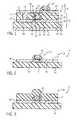
- a multilayer integrated circuit 9includes a first integrated circuit 10 and a second integrated circuit 11 .
- Circuit 10is preferably a first semiconductor-on-insulator (SOI) layer, and circuit 11 is preferably a second layer.
- First integrated circuit 10is stacked below second integrated circuit 11 .
- Circuit 11can be built on a recrystallized film as described below with reference to FIGS. 1-7.
- Circuit 10includes an insulating layer 14 , an active layer or a semiconductor substrate 18 , and an insulating layer 22 . Circuit 10 can also include a support substrate 12 . Circuit 10 is a SOI-based layer, substrate or platform.
- Support substrate 12is preferably a semiconductor material.
- Support substrate 12can also be an insulating material or other base layer for integrated circuit 10 .
- Support substrate 12can be silicon dioxide, silicon, polyester, or a flexible material.
- Insulating layer 14is preferably a buried oxide layer, such as a silicon dioxide layer, disposed between substrate 18 and substrate 12 .
- Active layer or semiconductor substrate 18is preferably a very thin silicon film separated from support substrate 12 by insulating layer 14 .
- semiconductor substrate 18is 200-800 angstroms ( ⁇ ) thick and insulating layer 14 is 2,000-3,000 ⁇ thick. In one embodiment, substrate 18 can be 200-500 ⁇ thick.
- Insulating layers 14 and 22can be any dielectric or insulating material.
- layer 22is a deposited high-temperature oxide, such as, chemical vapor deposited (CVD) tetraethylorthosilicate (TEOS) oxide, silicon dioxide, spin-on-glass (SOG), plasma enhanced CVD (PECVD) TEOS oxide, SiH-based oxide, PECVD oxide, or a two-layer glass and nitride material.
- layer 14can be formed similar to layer 22 .
- layer 14can be formed via an oxygen ion implantation process.
- Semiconductor substrate 18preferably includes active regions, such as, doped regions utilized in the formation of transistors, such as, transistor 50 .
- Active layer or substrate 18can include an N-type or P-type well.
- Active layer or substrate 18is preferably a single crystalline silicon substrate or other suitable material for transistor 50 .
- Doped regions in substrate 18can include a source region 60 and a drain region 62 .
- Transistor 50can include a gate structure 64 disposed between regions 60 and 62 .
- Gate structure 64can include spacer 39 , a gate dielectric layer 34 , and a polysilicon conductor 36 .
- Gate structure 64 , source 60 and drain 62can be silicided in accordance with conventional fabrication techniques.
- Gate stack or structure 64includes a gate dielectric layer 34 and a gate conductor 36 .
- Dielectric layer 34is preferably comprised of a thermally grown, 15-25 ⁇ thick, silicon dioxide material. Alternatively, deposited silicon nitride (Si 3 N 4 ) material or high-K gate dielectric materials can be utilized.
- Gate structure 64can also include a pair of sidewall spacers 39 .
- Spacers 39can be manufactured in a conventional silicon dioxide deposition and etch-back process. Alternatively, other insulative material such as nitride can be utilized to form spacers 39 .
- Conductor 36is preferably deposited as polysilicon by chemical vapor deposition (CVD) and etched to form the particular structure for transistor 12 .
- Conductor 36is preferably doped polysilicon.
- conductor 36can include metal, such as a refractory metal, or germanium to adjust the work function of transistor 50 .
- Gate structure 64has a height or thickness of 800-1200 ⁇ .
- Regions 60 and 62extend from a top surface 27 of layer 18 to a top surface 25 of layer 14 .
- Regions 60 and 62are preferably 300-800 ⁇ from top surface 27 to top surface 25 of layer 14 (junction depth) and can include a source extension and a drain extension below top surface 27 .
- the extensionsare preferably ultra-shallow.
- regions 60 and 62are heavily doped with N-type dopants (e.g., 5 ⁇ 10 19 ⁇ 1 ⁇ 10 20 dopants per cubic centimeter).
- regions 60 and 62are heavily doped with P-type dopants (e.g., 5 ⁇ 10 19 ⁇ 1 ⁇ 10 20 dopants per cubic centimeter).
- Appropriate dopants for a P-channel transistorinclude boron, boron diflouride, or iridium, and appropriate dopants for an N-channel transistor include arsenic, phosphorous, or antimony.
- Transistor 50can be a P-channel or N-channel metal oxide semiconductor field effect transistor (MOSFET), a floating gate transistor, or other electronic device.
- MOSFETmetal oxide semiconductor field effect transistor
- Transistor 50is preferably embodied as a fully depleted (FD) SOI MOSFET.
- a channel region 41is disposed below gate structure 64 .
- Channel region 41can be doped according to conventional processes. Also, region 41 can be fabricated to have increased charge carrier mobility.
- Channel region 41has a width slightly less than the gate length of gate structure 64 (e.g., 35 nm-100 nm).
- Region 41can advantageously include a semiconductor containing germanium for increased charge carrier mobility. The width of region 41 is downwardly diverging, having a narrower width at a junction with gate structure 64 than the width near surface 25 of layer 14 .
- Isolation regions 66can be insulating regions, such as, silicon dioxide regions formed in conventional local oxidation of silicon (LOCOS) processes. Alternatively, the isolation regions can be formed in a shallow trench isolation (STI) process. Circuit 10 can include any number and type of semiconductor elements in and above layer 18 .
- Integrated circuit 11is shown including an active layer or semiconductor substrate 24 .
- Semiconductor substrate 24is similar to semiconductor substrate 18 and houses a transistor 52 .
- Substrate 18is preferably a single crystalline semiconductor material (most preferably silicon). Therefore, circuit 9 includes multiple active layers which house semiconductor elements, such as, transistors 50 and 52 , on two separate active layers, such as, substrates 18 and 24 .
- Transistor 52is similar to transistor 50 .
- Transistors 50 and 52can be any type of semiconductor elements including CMOS FETS, FETS, diodes, floating gate transistors, resistors, or other devices which utilize active regions.
- Substrate 24can also include isolation regions. Substrate 24 is preferably doped to form active regions associated with transistor 52 .
- Circuit 11may include an insulating layer similar to insulating layer 22 above substrate 24 .
- metal layers or conductive layerscan be provided over the insulating layer above layer 24 .
- the metal layerscan include vias for connecting circuitry between circuits 10 and 11 .
- the viascan extend from multiple metal layers to substrates 18 and 24 .
- Substrates 24 and 18are coupled together or physically attached through a seeding window 75 .
- seeding window 75is filled with the material associated with substrate 24 .
- Window 75can be a via or aperture approximately 0.3-1.5 micrometer wide.
- Window 75can have a horizontal cross-section in a variety of shapes including circles, squares, rectangles, etc. As shown in FIG. 1, window 75 connects source region 60 of transistor 50 with a source region of transistor 52 .
- Layer 22is preferably approximately 2000-3000 ⁇ thick and has a smooth planar surface 23 .
- Window 75can be utilized as a short circuit between substrates 24 and 18 or for contacts to various conductors including gate conductors, back gate conductors, or other structures depending upon layout and design for circuit 9 .
- Window 75can also be covered within a trench isolation process.
- Window 75is utilized by proper seeding for substrate 18 as discussed below with reference to FIGS. 6-7.
- circuit 9can utilize vias that only travel through a single insulating layer 22 to connect substrates 24 and 18 . Unlike conventional processes, entire wafers do not need to be traversed because substrate 18 is formed directly on top of layer 22 .
- integrated circuit 10is disposed on an SOI substrate and includes active layer or substrate 18 and transistor 50 .
- Transistor 50can be fabricated on substrate 18 in accordance with any number of conventional transistor fabrication techniques.
- Layer 14 and substrate 18can be all or part of a silicon-on-insulator (SOI) wafer.
- SOIsilicon-on-insulator
- Such a wafercan be purchased from a variety of sources, or can be manufactured by implanting oxygen into a bulk semiconductor substrate.
- the SOI wafercan be formed by placing an epitaxial silicon layer on top of an insulating layer 22 .
- Transistor 50is built at least partially within substrate 18 (e.g., includes source 60 and drain 62 below top surface 27 of substrate 18 ). Transistor 50 can be fabricated in a variety of processes. For example, conventional deposition, etching and fabrication processes can be utilized to form transistor 50 .
- insulating layer 22is deposited above transistor 50 and substrate 18 .
- Layer 22is preferably deposited after transistor 50 is completed.
- Layer 22is deposited on top of transistor 50 and over substrate 18 .
- Layer 22can be a 4,000-5,000 ⁇ thick silicon dioxide layer deposited in a TEOS-based chemical vapor deposition (CVD) process.
- insulating layer 22is polished to remove approximately 2,000 ⁇ of material.
- layer 22can be polished in a chemical-mechanical polish (CMP) process to leave approximately 2,000-3,000 ⁇ of material having a planar top surface 23 .
- CMPchemical-mechanical polish
- layer 22can be subjected to a chemical etch to remove an additional 50 A of material. The chemical etch enhances the smoothness of surface 23 .
- a photolithographic processis utilized to form a seeding window 75 in layer 22 .
- layer 22is etched in accordance with a photolithographic mask to form seeding window 75 .
- the etching processis a dry etch process selective to silicon dioxide.
- Window 75is etched until top surface 27 of substrate 18 is reached.
- a conformal layer 76is deposited in window 75 and above surface 23 of layer 22 .
- Layer 76is preferably associated with substrate 24 (FIG. 1 ).
- Layer 76can be an amorphous semiconductor layer, such as, an amorphous silicon layer.
- Layer 76is preferably deposited as a thin layer ( 200 - 500 ⁇ thick) by CVD or PECVD. The thickness of layer 76 is measured from surface 23 of layer 22 to surface 79 of layer 76 .
- layer 76 and integrated circuit 10are subject to a thermal process, such as, an annealing process.
- a very low temperature furnace annealing processis utilized to melt layer 76 (e.g., at 450-550° C.).
- other annealing processescan be utilized.
- an excimer laser beam having a 308 nm wavelengthcan heat layer 76 .
- the laser energymelts layer 76 to form a single crystalline substrate 18 .
- RTArapid thermal annealing
- Solid phase epitaxyrefers to a crystallization process by which an amorphous semiconductor film (silicon, silicon/germanium, or germanium) is converted into crystalline semiconductor (silicon, silicon/germanium, or germanium) of a single orientation matching the orientation of an existing crystal structure (silicon, silicon/germanium, or germanium) start layer.
- Solid phase epitaxyis usually achieved by heating the amorphous semiconductor layer. Alternatively, a low temperature (e.g., 550-600° C.) rapid thermal anneal can be utilized.
- Seeding window 75allows substrate 18 to be utilized as a start or seeding layer for substrate 24 .
- substrate 24is recrystallized as single crystalline material.
- transistor 52is formed according to a process similar for forming transistor 50 .
- transistor 52After transistor 52 is formed, conventional semiconductor processes are utilized to complete integrated circuit 11 . Various CMOS processes can be utilized to interconnect transistors 50 and 52 . After transistor 52 is formed, further deposition steps and etching and photolithography steps can be utilized to form other conductive, semiconductive, and insulative structures. The conventional processes can include major pad contact formation and interconnect formation for connections between substrates 18 and 24 .
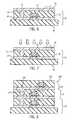
- an integrated circuit 109includes integrated circuits 110 , 111 and 112 .
- Integrated circuit 110is similar to integrated circuit 10 discussed with reference to FIG. 1 .
- Integrated circuit 111is similar to integrated circuit 11 discussed with reference to FIG. 1 .
- Integrated circuit 112is also similar to integrated circuit 111 and is provided above integrated circuit 111 according to the same process steps discussed with reference to FIGS. 1-7.
- an insulating layer 122is deposited over transistor 52 .
- a technique similar to the technique utilized to form substrate 18forms substrate 118 .
- Substrate 118is similar to substrate 18 (FIG. 1 ). Therefore, FIG. 8 shows an integrated circuit 109 including three active layers.
- a further insulating layer 120can be provided above integrated circuit 112 .
- Metal layers or yet another active layercan be provided above layer 120 .
- transistor 50has near ideal subthreshold voltage slope, low junction capacitance, an effective isolation, and increased current density.
- Transistor 50can have a non-floating (e.g., a biased) substrate to reduce floating substrate effects, such as, current and voltage kinks, thermal degradation, and large voltage variations.
Landscapes
- Thin Film Transistor (AREA)
- Metal-Oxide And Bipolar Metal-Oxide Semiconductor Integrated Circuits (AREA)
Abstract
Description
Claims (20)
Priority Applications (1)
| Application Number | Priority Date | Filing Date | Title |
|---|---|---|---|
| US09/633,208US6429484B1 (en) | 2000-08-07 | 2000-08-07 | Multiple active layer structure and a method of making such a structure |
Applications Claiming Priority (1)
| Application Number | Priority Date | Filing Date | Title |
|---|---|---|---|
| US09/633,208US6429484B1 (en) | 2000-08-07 | 2000-08-07 | Multiple active layer structure and a method of making such a structure |
Publications (1)
| Publication Number | Publication Date |
|---|---|
| US6429484B1true US6429484B1 (en) | 2002-08-06 |
Family
ID=24538688
Family Applications (1)
| Application Number | Title | Priority Date | Filing Date |
|---|---|---|---|
| US09/633,208Expired - LifetimeUS6429484B1 (en) | 2000-08-07 | 2000-08-07 | Multiple active layer structure and a method of making such a structure |
Country Status (1)
| Country | Link |
|---|---|
| US (1) | US6429484B1 (en) |
Cited By (278)
| Publication number | Priority date | Publication date | Assignee | Title |
|---|---|---|---|---|
| US6596597B2 (en)* | 2001-06-12 | 2003-07-22 | International Business Machines Corporation | Method of manufacturing dual gate logic devices |
| US6809334B2 (en)* | 2001-03-30 | 2004-10-26 | Renesas Technology Corp. | Semiconductor integrated circuit device, and method of manufacturing the same |
| US20040219722A1 (en)* | 2003-05-01 | 2004-11-04 | Pham Daniel T. | Method for forming a double-gated semiconductor device |
| US20050042808A1 (en)* | 2003-03-10 | 2005-02-24 | Nec Electronics Corporation | Semiconductor device and method of fabricating the same |
| US20050067619A1 (en)* | 2003-09-18 | 2005-03-31 | Sharp Kabushiki Kaisha | Thin film semiconductor device and fabrication method therefor |
| JP2005203777A (en)* | 2004-01-12 | 2005-07-28 | Samsung Electronics Co Ltd | Semiconductor integrated circuit for adopting laminated node-contact structure and laminated thin-film transistor, and manufacturing method thereof |
| US20050280154A1 (en)* | 2004-06-21 | 2005-12-22 | Sang-Yun Lee | Semiconductor memory device |
| US20050285162A1 (en)* | 2004-06-25 | 2005-12-29 | Chul-Sung Kim | Semiconductor devices having a stacked structure and methods of forming the same |
| US20060011978A1 (en)* | 2003-03-11 | 2006-01-19 | Arup Bhattacharyya | Semiconductor constructions and integrated circuits |
| US20060076548A1 (en)* | 2004-10-08 | 2006-04-13 | Samsung Electronics Co., Ltd. | PRAMs having a plurality of active regions located vertically in sequence and methods of forming the same |
| US20060097328A1 (en)* | 2004-11-08 | 2006-05-11 | Kim Sung-Jin | SRAM cells having landing pad in contact with upper and lower cell gate patterns and methods of forming the same |
| US20060097319A1 (en)* | 2004-11-05 | 2006-05-11 | Samsung Electronics Co., Ltd. | Method of forming single crystal semiconductor thin film on insulator and semiconductor device fabricated thereby |
| KR100580640B1 (en) | 2004-12-17 | 2006-05-16 | 삼성전자주식회사 | Manufacturing method of polycrystalline silicon film and manufacturing method of multilayer transistor using same |
| US20060102959A1 (en)* | 2004-11-16 | 2006-05-18 | Samsung Electronics Co., Ltd. | Semiconductor integrated circuit devices having single crystalline thin film transistors and methods of fabricating the same |
| US20060118872A1 (en)* | 2004-12-08 | 2006-06-08 | Seiko Epson Corporation | Semiconductor device and method of manufacturing the same |
| US20060125058A1 (en)* | 2001-02-28 | 2006-06-15 | Fernando Gonzalez | Semiconductor circuitry constructions |
| US20060154453A1 (en)* | 2005-01-13 | 2006-07-13 | Yong-Hoon Son | Method(s) of forming a thin layer |
| US20060163571A1 (en)* | 2005-01-27 | 2006-07-27 | Samsung Electronics Co., Ltd. | Test element group structures having 3 dimensional SRAM cell transistors |
| KR100611112B1 (en) | 2005-01-20 | 2006-08-09 | 삼성전자주식회사 | A single crystal structure and a method of forming the same, a semiconductor device comprising the single crystal structure and a method of manufacturing the same. |
| US20060237725A1 (en)* | 2005-04-20 | 2006-10-26 | Samsung Electronics Co., Ltd. | Semiconductor devices having thin film transistors and methods of fabricating the same |
| US20060270215A1 (en)* | 2005-05-30 | 2006-11-30 | Samsung Electronics Co., Ltd. | Semiconductor device and method of manufacturing the same |
| US20060275962A1 (en)* | 2003-06-24 | 2006-12-07 | Sang-Yun Lee | Three-dimensional integrated circuit structure and method of making same |
| US20070007532A1 (en)* | 2005-07-08 | 2007-01-11 | Sung-Kwan Kang | Stacked semiconductor device and related method |
| US20070045671A1 (en)* | 2005-08-17 | 2007-03-01 | Sung-Jun Kim | Multi-level transistor and related method |
| KR100714401B1 (en)* | 2006-02-08 | 2007-05-04 | 삼성전자주식회사 | A semiconductor device having a stacked transistor and a method of forming the same |
| US20070138541A1 (en)* | 2003-06-16 | 2007-06-21 | Samsung Electronics Co., Ltd. | Method of erasing data from SONOS memory device |
| US20070165455A1 (en)* | 2005-12-12 | 2007-07-19 | Jae-Kwan Park | NAND-type non-volatile memory devices having a stacked structure and associated methods of forming and operating the same |
| US20070170433A1 (en)* | 2006-01-24 | 2007-07-26 | Samsung Electronics Co., Ltd. | Multilevel semiconductor device and method of manufacturing the same |
| US20070181880A1 (en)* | 2006-02-08 | 2007-08-09 | Samsung Electronics Co., Ltd. | Semiconductor device and method for forming the same |
| US20080023770A1 (en)* | 2006-07-26 | 2008-01-31 | Samsung Electronics Co., Ltd. | Stacked semiconductor devices and methods of manufacturing the same |
| US20080061371A1 (en)* | 2004-05-17 | 2008-03-13 | Samsung Electronics Co., Ltd. | Field effect transistor (fet) devices and methods of manufacturing fet devices |
| US20080073717A1 (en)* | 2006-09-26 | 2008-03-27 | Tae-Hong Ha | Semiconductor devices having substrate plug and methods of forming the same |
| US7368333B2 (en) | 2005-05-24 | 2008-05-06 | Samsung Electronics Co., Ltd. | Semiconductor device and method of manufacturing the same by using atomic layer deposition |
| US20090001503A1 (en)* | 2007-06-28 | 2009-01-01 | Samsung Electronics Co., Ltd. | Semiconductor device having floating body element and bulk body element and method of manufacturing the same |
| US20090020817A1 (en)* | 2007-07-20 | 2009-01-22 | Samsung Electronics Co., Ltd. | Semiconductor device having a plurality of stacked transistors and method of fabricating the same |
| US20090160012A1 (en)* | 2007-12-21 | 2009-06-25 | Sang-Chul Kim | Semiconductor device and method for fabricating the same |
| US20090258462A1 (en)* | 2004-09-29 | 2009-10-15 | Konevecki Michael W | Method for forming doped polysilicon via connecting polysilicon layers |
| US20100035429A1 (en)* | 2007-01-18 | 2010-02-11 | Terasemicon Corporation | Method for fabricating semiconductor device |
| US20100117152A1 (en)* | 2007-06-28 | 2010-05-13 | Chang-Woo Oh | Semiconductor devices |
| US20100259296A1 (en)* | 2009-04-14 | 2010-10-14 | Zvi Or-Bach | Method for fabrication of a semiconductor device and structure |
| US20110089523A1 (en)* | 2008-12-10 | 2011-04-21 | Ultratech, Inc. | Systems and processes for forming three-dimensional circuits |
| US20110199116A1 (en)* | 2010-02-16 | 2011-08-18 | NuPGA Corporation | Method for fabrication of a semiconductor device and structure |
| US20120009752A1 (en)* | 2008-06-23 | 2012-01-12 | Fujitsu Semiconductor Limited | Method for manufacturing semiconductor device |
| US20120012837A1 (en)* | 2010-07-16 | 2012-01-19 | Semiconductor Energy Laboratory Co., Ltd. | Semiconductor device |
| JP2012033906A (en)* | 2010-07-02 | 2012-02-16 | Semiconductor Energy Lab Co Ltd | Semiconductor device |
| US20120040506A1 (en)* | 2008-02-29 | 2012-02-16 | Hynix Semiconductor Inc. | Method for Forming Semiconductor Device |
| US8163581B1 (en) | 2010-10-13 | 2012-04-24 | Monolith IC 3D | Semiconductor and optoelectronic devices |
| US8203148B2 (en) | 2010-10-11 | 2012-06-19 | Monolithic 3D Inc. | Semiconductor device and structure |
| US8237228B2 (en) | 2009-10-12 | 2012-08-07 | Monolithic 3D Inc. | System comprising a semiconductor device and structure |
| US8258810B2 (en) | 2010-09-30 | 2012-09-04 | Monolithic 3D Inc. | 3D semiconductor device |
| US8273610B2 (en) | 2010-11-18 | 2012-09-25 | Monolithic 3D Inc. | Method of constructing a semiconductor device and structure |
| US8283215B2 (en) | 2010-10-13 | 2012-10-09 | Monolithic 3D Inc. | Semiconductor and optoelectronic devices |
| US8294159B2 (en) | 2009-10-12 | 2012-10-23 | Monolithic 3D Inc. | Method for fabrication of a semiconductor device and structure |
| US8298875B1 (en) | 2011-03-06 | 2012-10-30 | Monolithic 3D Inc. | Method for fabrication of a semiconductor device and structure |
| US8362482B2 (en) | 2009-04-14 | 2013-01-29 | Monolithic 3D Inc. | Semiconductor device and structure |
| US8362800B2 (en) | 2010-10-13 | 2013-01-29 | Monolithic 3D Inc. | 3D semiconductor device including field repairable logics |
| US8373439B2 (en) | 2009-04-14 | 2013-02-12 | Monolithic 3D Inc. | 3D semiconductor device |
| US8373230B1 (en) | 2010-10-13 | 2013-02-12 | Monolithic 3D Inc. | Method for fabrication of a semiconductor device and structure |
| US8378494B2 (en) | 2009-04-14 | 2013-02-19 | Monolithic 3D Inc. | Method for fabrication of a semiconductor device and structure |
| US8378715B2 (en) | 2009-04-14 | 2013-02-19 | Monolithic 3D Inc. | Method to construct systems |
| US8379458B1 (en) | 2010-10-13 | 2013-02-19 | Monolithic 3D Inc. | Semiconductor device and structure |
| US8384426B2 (en) | 2009-04-14 | 2013-02-26 | Monolithic 3D Inc. | Semiconductor device and structure |
| US8405420B2 (en) | 2009-04-14 | 2013-03-26 | Monolithic 3D Inc. | System comprising a semiconductor device and structure |
| US8427200B2 (en) | 2009-04-14 | 2013-04-23 | Monolithic 3D Inc. | 3D semiconductor device |
| US8440542B2 (en) | 2010-10-11 | 2013-05-14 | Monolithic 3D Inc. | Semiconductor device and structure |
| US8450804B2 (en) | 2011-03-06 | 2013-05-28 | Monolithic 3D Inc. | Semiconductor device and structure for heat removal |
| US8461035B1 (en) | 2010-09-30 | 2013-06-11 | Monolithic 3D Inc. | Method for fabrication of a semiconductor device and structure |
| US8476145B2 (en) | 2010-10-13 | 2013-07-02 | Monolithic 3D Inc. | Method of fabricating a semiconductor device and structure |
| US8492886B2 (en) | 2010-02-16 | 2013-07-23 | Monolithic 3D Inc | 3D integrated circuit with logic |
| US8536023B2 (en) | 2010-11-22 | 2013-09-17 | Monolithic 3D Inc. | Method of manufacturing a semiconductor device and structure |
| US8541819B1 (en) | 2010-12-09 | 2013-09-24 | Monolithic 3D Inc. | Semiconductor device and structure |
| US8557632B1 (en) | 2012-04-09 | 2013-10-15 | Monolithic 3D Inc. | Method for fabrication of a semiconductor device and structure |
| US8574929B1 (en) | 2012-11-16 | 2013-11-05 | Monolithic 3D Inc. | Method to form a 3D semiconductor device and structure |
| US8581349B1 (en)* | 2011-05-02 | 2013-11-12 | Monolithic 3D Inc. | 3D memory semiconductor device and structure |
| US8642416B2 (en) | 2010-07-30 | 2014-02-04 | Monolithic 3D Inc. | Method of forming three dimensional integrated circuit devices using layer transfer technique |
| US8669778B1 (en) | 2009-04-14 | 2014-03-11 | Monolithic 3D Inc. | Method for design and manufacturing of a 3D semiconductor device |
| US8674470B1 (en) | 2012-12-22 | 2014-03-18 | Monolithic 3D Inc. | Semiconductor device and structure |
| US8686428B1 (en) | 2012-11-16 | 2014-04-01 | Monolithic 3D Inc. | Semiconductor device and structure |
| US8685805B2 (en) | 2004-08-06 | 2014-04-01 | Samsung Electronics Co., Ltd. | Semiconductor devices with connection patterns |
| US8687399B2 (en) | 2011-10-02 | 2014-04-01 | Monolithic 3D Inc. | Semiconductor device and structure |
| US8709880B2 (en) | 2010-07-30 | 2014-04-29 | Monolithic 3D Inc | Method for fabrication of a semiconductor device and structure |
| US8742476B1 (en) | 2012-11-27 | 2014-06-03 | Monolithic 3D Inc. | Semiconductor device and structure |
| US8754533B2 (en) | 2009-04-14 | 2014-06-17 | Monolithic 3D Inc. | Monolithic three-dimensional semiconductor device and structure |
| US8803206B1 (en) | 2012-12-29 | 2014-08-12 | Monolithic 3D Inc. | 3D semiconductor device and structure |
| US8901613B2 (en) | 2011-03-06 | 2014-12-02 | Monolithic 3D Inc. | Semiconductor device and structure for heat removal |
| US8902663B1 (en) | 2013-03-11 | 2014-12-02 | Monolithic 3D Inc. | Method of maintaining a memory state |
| US8975670B2 (en) | 2011-03-06 | 2015-03-10 | Monolithic 3D Inc. | Semiconductor device and structure for heat removal |
| US8994404B1 (en) | 2013-03-12 | 2015-03-31 | Monolithic 3D Inc. | Semiconductor device and structure |
| US9000557B2 (en) | 2012-03-17 | 2015-04-07 | Zvi Or-Bach | Semiconductor device and structure |
| US9029173B2 (en) | 2011-10-18 | 2015-05-12 | Monolithic 3D Inc. | Method for fabrication of a semiconductor device and structure |
| US9099424B1 (en) | 2012-08-10 | 2015-08-04 | Monolithic 3D Inc. | Semiconductor system, device and structure with heat removal |
| US9099526B2 (en) | 2010-02-16 | 2015-08-04 | Monolithic 3D Inc. | Integrated circuit device and structure |
| US9117749B1 (en) | 2013-03-15 | 2015-08-25 | Monolithic 3D Inc. | Semiconductor device and structure |
| US9197804B1 (en) | 2011-10-14 | 2015-11-24 | Monolithic 3D Inc. | Semiconductor and optoelectronic devices |
| US9219005B2 (en) | 2011-06-28 | 2015-12-22 | Monolithic 3D Inc. | Semiconductor system and device |
| US20160086980A1 (en)* | 2013-07-29 | 2016-03-24 | Efficient Power Conversion Corporation | Gan transistors with polysilicon layers used for creating additional components |
| US9391090B2 (en) | 2014-08-21 | 2016-07-12 | Samsung Electronics Co., Ltd. | Integrated circuit device including polycrystalline semiconductor film and method of manufacturing the same |
| US9425213B1 (en)* | 2015-06-30 | 2016-08-23 | Stmicroelectronics, Inc. | Stacked short and long channel FinFETs |
| US9509313B2 (en) | 2009-04-14 | 2016-11-29 | Monolithic 3D Inc. | 3D semiconductor device |
| US9577642B2 (en) | 2009-04-14 | 2017-02-21 | Monolithic 3D Inc. | Method to form a 3D semiconductor device |
| US20170092541A1 (en)* | 2009-10-12 | 2017-03-30 | Monolithic 3D Inc. | 3d semiconductor device and structure |
| US9711407B2 (en) | 2009-04-14 | 2017-07-18 | Monolithic 3D Inc. | Method of manufacturing a three dimensional integrated circuit by transfer of a mono-crystalline layer |
| US9871034B1 (en) | 2012-12-29 | 2018-01-16 | Monolithic 3D Inc. | Semiconductor device and structure |
| US9953925B2 (en) | 2011-06-28 | 2018-04-24 | Monolithic 3D Inc. | Semiconductor system and device |
| US10043833B2 (en) | 2011-12-01 | 2018-08-07 | Semiconductor Energy Laboratory Co., Ltd. | Semiconductor device |
| US10043781B2 (en) | 2009-10-12 | 2018-08-07 | Monolithic 3D Inc. | 3D semiconductor device and structure |
| US10115663B2 (en) | 2012-12-29 | 2018-10-30 | Monolithic 3D Inc. | 3D semiconductor device and structure |
| US10127344B2 (en) | 2013-04-15 | 2018-11-13 | Monolithic 3D Inc. | Automation for monolithic 3D devices |
| US10157909B2 (en) | 2009-10-12 | 2018-12-18 | Monolithic 3D Inc. | 3D semiconductor device and structure |
| US10170249B2 (en) | 2017-01-31 | 2019-01-01 | International Business Machines Corporation | Multi-layer capacitor package |
| US10217667B2 (en) | 2011-06-28 | 2019-02-26 | Monolithic 3D Inc. | 3D semiconductor device, fabrication method and system |
| US10224279B2 (en) | 2013-03-15 | 2019-03-05 | Monolithic 3D Inc. | Semiconductor device and structure |
| US10290682B2 (en) | 2010-10-11 | 2019-05-14 | Monolithic 3D Inc. | 3D IC semiconductor device and structure with stacked memory |
| US10297586B2 (en) | 2015-03-09 | 2019-05-21 | Monolithic 3D Inc. | Methods for processing a 3D semiconductor device |
| US10325651B2 (en) | 2013-03-11 | 2019-06-18 | Monolithic 3D Inc. | 3D semiconductor device with stacked memory |
| US10354995B2 (en) | 2009-10-12 | 2019-07-16 | Monolithic 3D Inc. | Semiconductor memory device and structure |
| US10366970B2 (en) | 2009-10-12 | 2019-07-30 | Monolithic 3D Inc. | 3D semiconductor device and structure |
| US10381328B2 (en) | 2015-04-19 | 2019-08-13 | Monolithic 3D Inc. | Semiconductor device and structure |
| US10388863B2 (en) | 2009-10-12 | 2019-08-20 | Monolithic 3D Inc. | 3D memory device and structure |
| US10388568B2 (en) | 2011-06-28 | 2019-08-20 | Monolithic 3D Inc. | 3D semiconductor device and system |
| US10418369B2 (en) | 2015-10-24 | 2019-09-17 | Monolithic 3D Inc. | Multi-level semiconductor memory device and structure |
| US10497713B2 (en) | 2010-11-18 | 2019-12-03 | Monolithic 3D Inc. | 3D semiconductor memory device and structure |
| US10515935B2 (en)* | 2012-12-22 | 2019-12-24 | Monolithic 3D Inc. | 3D semiconductor device and structure |
| US10515981B2 (en) | 2015-09-21 | 2019-12-24 | Monolithic 3D Inc. | Multilevel semiconductor device and structure with memory |
| US10522225B1 (en) | 2015-10-02 | 2019-12-31 | Monolithic 3D Inc. | Semiconductor device with non-volatile memory |
| US10600888B2 (en) | 2012-04-09 | 2020-03-24 | Monolithic 3D Inc. | 3D semiconductor device |
| US10600657B2 (en) | 2012-12-29 | 2020-03-24 | Monolithic 3D Inc | 3D semiconductor device and structure |
| US10651054B2 (en) | 2012-12-29 | 2020-05-12 | Monolithic 3D Inc. | 3D semiconductor device and structure |
| US10679977B2 (en) | 2010-10-13 | 2020-06-09 | Monolithic 3D Inc. | 3D microdisplay device and structure |
| US10825779B2 (en) | 2015-04-19 | 2020-11-03 | Monolithic 3D Inc. | 3D semiconductor device and structure |
| US10833108B2 (en) | 2010-10-13 | 2020-11-10 | Monolithic 3D Inc. | 3D microdisplay device and structure |
| US10840239B2 (en) | 2014-08-26 | 2020-11-17 | Monolithic 3D Inc. | 3D semiconductor device and structure |
| US10847540B2 (en) | 2015-10-24 | 2020-11-24 | Monolithic 3D Inc. | 3D semiconductor memory device and structure |
| US10892169B2 (en) | 2012-12-29 | 2021-01-12 | Monolithic 3D Inc. | 3D semiconductor device and structure |
| US10892016B1 (en) | 2019-04-08 | 2021-01-12 | Monolithic 3D Inc. | 3D memory semiconductor devices and structures |
| US10896931B1 (en) | 2010-10-11 | 2021-01-19 | Monolithic 3D Inc. | 3D semiconductor device and structure |
| US10903089B1 (en) | 2012-12-29 | 2021-01-26 | Monolithic 3D Inc. | 3D semiconductor device and structure |
| US10910364B2 (en) | 2009-10-12 | 2021-02-02 | Monolitaic 3D Inc. | 3D semiconductor device |
| US10943934B2 (en) | 2010-10-13 | 2021-03-09 | Monolithic 3D Inc. | Multilevel semiconductor device and structure |
| US10978501B1 (en) | 2010-10-13 | 2021-04-13 | Monolithic 3D Inc. | Multilevel semiconductor device and structure with waveguides |
| US10998374B1 (en) | 2010-10-13 | 2021-05-04 | Monolithic 3D Inc. | Multilevel semiconductor device and structure |
| US11004719B1 (en) | 2010-11-18 | 2021-05-11 | Monolithic 3D Inc. | Methods for producing a 3D semiconductor memory device and structure |
| US11004694B1 (en) | 2012-12-29 | 2021-05-11 | Monolithic 3D Inc. | 3D semiconductor device and structure |
| US11011507B1 (en) | 2015-04-19 | 2021-05-18 | Monolithic 3D Inc. | 3D semiconductor device and structure |
| US11018191B1 (en) | 2010-10-11 | 2021-05-25 | Monolithic 3D Inc. | 3D semiconductor device and structure |
| US11018133B2 (en) | 2009-10-12 | 2021-05-25 | Monolithic 3D Inc. | 3D integrated circuit |
| US11018042B1 (en) | 2010-11-18 | 2021-05-25 | Monolithic 3D Inc. | 3D semiconductor memory device and structure |
| US11018156B2 (en) | 2019-04-08 | 2021-05-25 | Monolithic 3D Inc. | 3D memory semiconductor devices and structures |
| US11018116B2 (en) | 2012-12-22 | 2021-05-25 | Monolithic 3D Inc. | Method to form a 3D semiconductor device and structure |
| US11024673B1 (en) | 2010-10-11 | 2021-06-01 | Monolithic 3D Inc. | 3D semiconductor device and structure |
| US11031275B2 (en) | 2010-11-18 | 2021-06-08 | Monolithic 3D Inc. | 3D semiconductor device and structure with memory |
| US11031394B1 (en) | 2014-01-28 | 2021-06-08 | Monolithic 3D Inc. | 3D semiconductor device and structure |
| US11030371B2 (en) | 2013-04-15 | 2021-06-08 | Monolithic 3D Inc. | Automation for monolithic 3D devices |
| US11043523B1 (en) | 2010-10-13 | 2021-06-22 | Monolithic 3D Inc. | Multilevel semiconductor device and structure with image sensors |
| US11056468B1 (en) | 2015-04-19 | 2021-07-06 | Monolithic 3D Inc. | 3D semiconductor device and structure |
| US11063071B1 (en) | 2010-10-13 | 2021-07-13 | Monolithic 3D Inc. | Multilevel semiconductor device and structure with waveguides |
| US11063024B1 (en) | 2012-12-22 | 2021-07-13 | Monlithic 3D Inc. | Method to form a 3D semiconductor device and structure |
| US11088050B2 (en) | 2012-04-09 | 2021-08-10 | Monolithic 3D Inc. | 3D semiconductor device with isolation layers |
| US11088130B2 (en) | 2014-01-28 | 2021-08-10 | Monolithic 3D Inc. | 3D semiconductor device and structure |
| US11087995B1 (en) | 2012-12-29 | 2021-08-10 | Monolithic 3D Inc. | 3D semiconductor device and structure |
| US11094576B1 (en) | 2010-11-18 | 2021-08-17 | Monolithic 3D Inc. | Methods for producing a 3D semiconductor memory device and structure |
| US11107808B1 (en) | 2014-01-28 | 2021-08-31 | Monolithic 3D Inc. | 3D semiconductor device and structure |
| US11107721B2 (en) | 2010-11-18 | 2021-08-31 | Monolithic 3D Inc. | 3D semiconductor device and structure with NAND logic |
| US11114464B2 (en) | 2015-10-24 | 2021-09-07 | Monolithic 3D Inc. | 3D semiconductor device and structure |
| US11114427B2 (en) | 2015-11-07 | 2021-09-07 | Monolithic 3D Inc. | 3D semiconductor processor and memory device and structure |
| US11121021B2 (en) | 2010-11-18 | 2021-09-14 | Monolithic 3D Inc. | 3D semiconductor device and structure |
| US11133344B2 (en) | 2010-10-13 | 2021-09-28 | Monolithic 3D Inc. | Multilevel semiconductor device and structure with image sensors |
| US11158652B1 (en) | 2019-04-08 | 2021-10-26 | Monolithic 3D Inc. | 3D memory semiconductor devices and structures |
| US11158534B2 (en)* | 2017-11-22 | 2021-10-26 | Taiwan Semiconductor Manufacturing Company, Ltd. | SOI substrate |
| US11158674B2 (en) | 2010-10-11 | 2021-10-26 | Monolithic 3D Inc. | Method to produce a 3D semiconductor device and structure |
| US11164770B1 (en) | 2010-11-18 | 2021-11-02 | Monolithic 3D Inc. | Method for producing a 3D semiconductor memory device and structure |
| US11164811B2 (en) | 2012-04-09 | 2021-11-02 | Monolithic 3D Inc. | 3D semiconductor device with isolation layers and oxide-to-oxide bonding |
| US11163112B2 (en) | 2010-10-13 | 2021-11-02 | Monolithic 3D Inc. | Multilevel semiconductor device and structure with electromagnetic modulators |
| US11164898B2 (en) | 2010-10-13 | 2021-11-02 | Monolithic 3D Inc. | Multilevel semiconductor device and structure |
| US11177140B2 (en) | 2012-12-29 | 2021-11-16 | Monolithic 3D Inc. | 3D semiconductor device and structure |
| US11211279B2 (en) | 2010-11-18 | 2021-12-28 | Monolithic 3D Inc. | Method for processing a 3D integrated circuit and structure |
| US11217565B2 (en) | 2012-12-22 | 2022-01-04 | Monolithic 3D Inc. | Method to form a 3D semiconductor device and structure |
| US11227897B2 (en) | 2010-10-11 | 2022-01-18 | Monolithic 3D Inc. | Method for producing a 3D semiconductor memory device and structure |
| US20220037324A1 (en)* | 2020-07-30 | 2022-02-03 | Micron Technology, Inc. | Digit line and body contact for semiconductor devices |
| US11251149B2 (en) | 2016-10-10 | 2022-02-15 | Monolithic 3D Inc. | 3D memory device and structure |
| US11257867B1 (en) | 2010-10-11 | 2022-02-22 | Monolithic 3D Inc. | 3D semiconductor device and structure with oxide bonds |
| US11270055B1 (en) | 2013-04-15 | 2022-03-08 | Monolithic 3D Inc. | Automation for monolithic 3D devices |
| TWI758562B (en)* | 2017-11-22 | 2022-03-21 | 台灣積體電路製造股份有限公司 | Semiconductor on insulator substrate and method for manufacturing the same |
| US11296115B1 (en) | 2015-10-24 | 2022-04-05 | Monolithic 3D Inc. | 3D semiconductor device and structure |
| US11296106B2 (en) | 2019-04-08 | 2022-04-05 | Monolithic 3D Inc. | 3D memory semiconductor devices and structures |
| US11309292B2 (en) | 2012-12-22 | 2022-04-19 | Monolithic 3D Inc. | 3D semiconductor device and structure with metal layers |
| US11315980B1 (en) | 2010-10-11 | 2022-04-26 | Monolithic 3D Inc. | 3D semiconductor device and structure with transistors |
| US11329059B1 (en) | 2016-10-10 | 2022-05-10 | Monolithic 3D Inc. | 3D memory devices and structures with thinned single crystal substrates |
| US11327227B2 (en) | 2010-10-13 | 2022-05-10 | Monolithic 3D Inc. | Multilevel semiconductor device and structure with electromagnetic modulators |
| US11341309B1 (en) | 2013-04-15 | 2022-05-24 | Monolithic 3D Inc. | Automation for monolithic 3D devices |
| US11355380B2 (en) | 2010-11-18 | 2022-06-07 | Monolithic 3D Inc. | Methods for producing 3D semiconductor memory device and structure utilizing alignment marks |
| US11355381B2 (en) | 2010-11-18 | 2022-06-07 | Monolithic 3D Inc. | 3D semiconductor memory device and structure |
| US11374118B2 (en) | 2009-10-12 | 2022-06-28 | Monolithic 3D Inc. | Method to form a 3D integrated circuit |
| US11398569B2 (en) | 2013-03-12 | 2022-07-26 | Monolithic 3D Inc. | 3D semiconductor device and structure |
| US11404466B2 (en) | 2010-10-13 | 2022-08-02 | Monolithic 3D Inc. | Multilevel semiconductor device and structure with image sensors |
| US11410912B2 (en) | 2012-04-09 | 2022-08-09 | Monolithic 3D Inc. | 3D semiconductor device with vias and isolation layers |
| US11430667B2 (en) | 2012-12-29 | 2022-08-30 | Monolithic 3D Inc. | 3D semiconductor device and structure with bonding |
| US11430668B2 (en) | 2012-12-29 | 2022-08-30 | Monolithic 3D Inc. | 3D semiconductor device and structure with bonding |
| US11437368B2 (en) | 2010-10-13 | 2022-09-06 | Monolithic 3D Inc. | Multilevel semiconductor device and structure with oxide bonding |
| US11443971B2 (en) | 2010-11-18 | 2022-09-13 | Monolithic 3D Inc. | 3D semiconductor device and structure with memory |
| US11469271B2 (en) | 2010-10-11 | 2022-10-11 | Monolithic 3D Inc. | Method to produce 3D semiconductor devices and structures with memory |
| US11476181B1 (en) | 2012-04-09 | 2022-10-18 | Monolithic 3D Inc. | 3D semiconductor device and structure with metal layers |
| US11482439B2 (en) | 2010-11-18 | 2022-10-25 | Monolithic 3D Inc. | Methods for producing a 3D semiconductor memory device comprising charge trap junction-less transistors |
| US11482438B2 (en) | 2010-11-18 | 2022-10-25 | Monolithic 3D Inc. | Methods for producing a 3D semiconductor memory device and structure |
| US11482440B2 (en) | 2010-12-16 | 2022-10-25 | Monolithic 3D Inc. | 3D semiconductor device and structure with a built-in test circuit for repairing faulty circuits |
| US11487928B2 (en) | 2013-04-15 | 2022-11-01 | Monolithic 3D Inc. | Automation for monolithic 3D devices |
| US11495484B2 (en) | 2010-11-18 | 2022-11-08 | Monolithic 3D Inc. | 3D semiconductor devices and structures with at least two single-crystal layers |
| US11508605B2 (en) | 2010-11-18 | 2022-11-22 | Monolithic 3D Inc. | 3D semiconductor memory device and structure |
| US11521888B2 (en) | 2010-11-18 | 2022-12-06 | Monolithic 3D Inc. | 3D semiconductor device and structure with high-k metal gate transistors |
| US11569117B2 (en) | 2010-11-18 | 2023-01-31 | Monolithic 3D Inc. | 3D semiconductor device and structure with single-crystal layers |
| US11574109B1 (en) | 2013-04-15 | 2023-02-07 | Monolithic 3D Inc | Automation methods for 3D integrated circuits and devices |
| US11594473B2 (en) | 2012-04-09 | 2023-02-28 | Monolithic 3D Inc. | 3D semiconductor device and structure with metal layers and a connective path |
| US11600667B1 (en) | 2010-10-11 | 2023-03-07 | Monolithic 3D Inc. | Method to produce 3D semiconductor devices and structures with memory |
| US11605663B2 (en) | 2010-10-13 | 2023-03-14 | Monolithic 3D Inc. | Multilevel semiconductor device and structure with image sensors and wafer bonding |
| US11610802B2 (en) | 2010-11-18 | 2023-03-21 | Monolithic 3D Inc. | Method for producing a 3D semiconductor device and structure with single crystal transistors and metal gate electrodes |
| US11615977B2 (en) | 2010-11-18 | 2023-03-28 | Monolithic 3D Inc. | 3D semiconductor memory device and structure |
| US11616004B1 (en) | 2012-04-09 | 2023-03-28 | Monolithic 3D Inc. | 3D semiconductor device and structure with metal layers and a connective path |
| US11694944B1 (en) | 2012-04-09 | 2023-07-04 | Monolithic 3D Inc. | 3D semiconductor device and structure with metal layers and a connective path |
| US11694922B2 (en) | 2010-10-13 | 2023-07-04 | Monolithic 3D Inc. | Multilevel semiconductor device and structure with oxide bonding |
| US11711928B2 (en) | 2016-10-10 | 2023-07-25 | Monolithic 3D Inc. | 3D memory devices and structures with control circuits |
| US11720736B2 (en) | 2013-04-15 | 2023-08-08 | Monolithic 3D Inc. | Automation methods for 3D integrated circuits and devices |
| US11735462B2 (en) | 2010-11-18 | 2023-08-22 | Monolithic 3D Inc. | 3D semiconductor device and structure with single-crystal layers |
| US11735501B1 (en) | 2012-04-09 | 2023-08-22 | Monolithic 3D Inc. | 3D semiconductor device and structure with metal layers and a connective path |
| US11763864B2 (en) | 2019-04-08 | 2023-09-19 | Monolithic 3D Inc. | 3D memory semiconductor devices and structures with bit-line pillars |
| US11784169B2 (en) | 2012-12-22 | 2023-10-10 | Monolithic 3D Inc. | 3D semiconductor device and structure with metal layers |
| US11784082B2 (en) | 2010-11-18 | 2023-10-10 | Monolithic 3D Inc. | 3D semiconductor device and structure with bonding |
| US11804396B2 (en) | 2010-11-18 | 2023-10-31 | Monolithic 3D Inc. | Methods for producing a 3D semiconductor device and structure with memory cells and multiple metal layers |
| US11812620B2 (en) | 2016-10-10 | 2023-11-07 | Monolithic 3D Inc. | 3D DRAM memory devices and structures with control circuits |
| US11854857B1 (en) | 2010-11-18 | 2023-12-26 | Monolithic 3D Inc. | Methods for producing a 3D semiconductor device and structure with memory cells and multiple metal layers |
| US11855100B2 (en) | 2010-10-13 | 2023-12-26 | Monolithic 3D Inc. | Multilevel semiconductor device and structure with oxide bonding |
| US11855114B2 (en) | 2010-10-13 | 2023-12-26 | Monolithic 3D Inc. | Multilevel semiconductor device and structure with image sensors and wafer bonding |
| US11862503B2 (en) | 2010-11-18 | 2024-01-02 | Monolithic 3D Inc. | Method for producing a 3D semiconductor device and structure with memory cells and multiple metal layers |
| US11869915B2 (en) | 2010-10-13 | 2024-01-09 | Monolithic 3D Inc. | Multilevel semiconductor device and structure with image sensors and wafer bonding |
| US11869591B2 (en) | 2016-10-10 | 2024-01-09 | Monolithic 3D Inc. | 3D memory devices and structures with control circuits |
| US11869965B2 (en) | 2013-03-11 | 2024-01-09 | Monolithic 3D Inc. | 3D semiconductor device and structure with metal layers and memory cells |
| US11881443B2 (en) | 2012-04-09 | 2024-01-23 | Monolithic 3D Inc. | 3D semiconductor device and structure with metal layers and a connective path |
| US11901210B2 (en) | 2010-11-18 | 2024-02-13 | Monolithic 3D Inc. | 3D semiconductor device and structure with memory |
| US11916045B2 (en) | 2012-12-22 | 2024-02-27 | Monolithic 3D Inc. | 3D semiconductor device and structure with metal layers |
| US11923374B2 (en) | 2013-03-12 | 2024-03-05 | Monolithic 3D Inc. | 3D semiconductor device and structure with metal layers |
| US11923230B1 (en) | 2010-11-18 | 2024-03-05 | Monolithic 3D Inc. | 3D semiconductor device and structure with bonding |
| US11930648B1 (en) | 2016-10-10 | 2024-03-12 | Monolithic 3D Inc. | 3D memory devices and structures with metal layers |
| US11929372B2 (en) | 2010-10-13 | 2024-03-12 | Monolithic 3D Inc. | Multilevel semiconductor device and structure with image sensors and wafer bonding |
| US11937422B2 (en) | 2015-11-07 | 2024-03-19 | Monolithic 3D Inc. | Semiconductor memory device and structure |
| US11935949B1 (en) | 2013-03-11 | 2024-03-19 | Monolithic 3D Inc. | 3D semiconductor device and structure with metal layers and memory cells |
| US11956952B2 (en) | 2015-08-23 | 2024-04-09 | Monolithic 3D Inc. | Semiconductor memory device and structure |
| US11961827B1 (en) | 2012-12-22 | 2024-04-16 | Monolithic 3D Inc. | 3D semiconductor device and structure with metal layers |
| US11967583B2 (en) | 2012-12-22 | 2024-04-23 | Monolithic 3D Inc. | 3D semiconductor device and structure with metal layers |
| US11978731B2 (en) | 2015-09-21 | 2024-05-07 | Monolithic 3D Inc. | Method to produce a multi-level semiconductor memory device and structure |
| US11984445B2 (en) | 2009-10-12 | 2024-05-14 | Monolithic 3D Inc. | 3D semiconductor devices and structures with metal layers |
| US11984438B2 (en) | 2010-10-13 | 2024-05-14 | Monolithic 3D Inc. | Multilevel semiconductor device and structure with oxide bonding |
| US11991884B1 (en) | 2015-10-24 | 2024-05-21 | Monolithic 3D Inc. | 3D semiconductor device and structure with logic and memory |
| US12016181B2 (en) | 2015-10-24 | 2024-06-18 | Monolithic 3D Inc. | 3D semiconductor device and structure with logic and memory |
| US12027518B1 (en) | 2009-10-12 | 2024-07-02 | Monolithic 3D Inc. | 3D semiconductor devices and structures with metal layers |
| US12035531B2 (en) | 2015-10-24 | 2024-07-09 | Monolithic 3D Inc. | 3D semiconductor device and structure with logic and memory |
| US12033884B2 (en) | 2010-11-18 | 2024-07-09 | Monolithic 3D Inc. | Methods for producing a 3D semiconductor device and structure with memory cells and multiple metal layers |
| US12051674B2 (en) | 2012-12-22 | 2024-07-30 | Monolithic 3D Inc. | 3D semiconductor device and structure with metal layers |
| US12068187B2 (en) | 2010-11-18 | 2024-08-20 | Monolithic 3D Inc. | 3D semiconductor device and structure with bonding and DRAM memory cells |
| US12080743B2 (en) | 2010-10-13 | 2024-09-03 | Monolithic 3D Inc. | Multilevel semiconductor device and structure with image sensors and wafer bonding |
| US12094829B2 (en) | 2014-01-28 | 2024-09-17 | Monolithic 3D Inc. | 3D semiconductor device and structure |
| US12094892B2 (en) | 2010-10-13 | 2024-09-17 | Monolithic 3D Inc. | 3D micro display device and structure |
| US12094965B2 (en) | 2013-03-11 | 2024-09-17 | Monolithic 3D Inc. | 3D semiconductor device and structure with metal layers and memory cells |
| US12100611B2 (en) | 2010-11-18 | 2024-09-24 | Monolithic 3D Inc. | Methods for producing a 3D semiconductor device and structure with memory cells and multiple metal layers |
| US12100658B2 (en) | 2015-09-21 | 2024-09-24 | Monolithic 3D Inc. | Method to produce a 3D multilayer semiconductor device and structure |
| US12100646B2 (en) | 2013-03-12 | 2024-09-24 | Monolithic 3D Inc. | 3D semiconductor device and structure with metal layers |
| US12120880B1 (en) | 2015-10-24 | 2024-10-15 | Monolithic 3D Inc. | 3D semiconductor device and structure with logic and memory |
| US12125737B1 (en) | 2010-11-18 | 2024-10-22 | Monolithic 3D Inc. | 3D semiconductor device and structure with metal layers and memory cells |
| US12136562B2 (en) | 2010-11-18 | 2024-11-05 | Monolithic 3D Inc. | 3D semiconductor device and structure with single-crystal layers |
| US12144190B2 (en) | 2010-11-18 | 2024-11-12 | Monolithic 3D Inc. | 3D semiconductor device and structure with bonding and memory cells preliminary class |
| US12154817B1 (en) | 2010-11-18 | 2024-11-26 | Monolithic 3D Inc. | Methods for producing a 3D semiconductor memory device and structure |
| US12178055B2 (en) | 2015-09-21 | 2024-12-24 | Monolithic 3D Inc. | 3D semiconductor memory devices and structures |
| US12219769B2 (en) | 2015-10-24 | 2025-02-04 | Monolithic 3D Inc. | 3D semiconductor device and structure with logic and memory |
| US12225704B2 (en) | 2016-10-10 | 2025-02-11 | Monolithic 3D Inc. | 3D memory devices and structures with memory arrays and metal layers |
| US12243765B2 (en) | 2010-11-18 | 2025-03-04 | Monolithic 3D Inc. | 3D semiconductor device and structure with metal layers and memory cells |
| US12250830B2 (en) | 2015-09-21 | 2025-03-11 | Monolithic 3D Inc. | 3D semiconductor memory devices and structures |
| US12249538B2 (en) | 2012-12-29 | 2025-03-11 | Monolithic 3D Inc. | 3D semiconductor device and structure including power distribution grids |
| US12272586B2 (en) | 2010-11-18 | 2025-04-08 | Monolithic 3D Inc. | 3D semiconductor memory device and structure with memory and metal layers |
| US12360310B2 (en) | 2010-10-13 | 2025-07-15 | Monolithic 3D Inc. | Multilevel semiconductor device and structure with oxide bonding |
| US12362219B2 (en) | 2010-11-18 | 2025-07-15 | Monolithic 3D Inc. | 3D semiconductor memory device and structure |
Citations (27)
| Publication number | Priority date | Publication date | Assignee | Title |
|---|---|---|---|---|
| US4272880A (en)* | 1979-04-20 | 1981-06-16 | Intel Corporation | MOS/SOS Process |
| US4381201A (en)* | 1980-03-11 | 1983-04-26 | Fujitsu Limited | Method for production of semiconductor devices |
| JPS61180466A (en) | 1985-02-06 | 1986-08-13 | Agency Of Ind Science & Technol | Stacked semiconductor device |
| US4996574A (en) | 1988-07-01 | 1991-02-26 | Fujitsu Limited | MIS transistor structure for increasing conductance between source and drain regions |
| US5041884A (en)* | 1990-10-11 | 1991-08-20 | Mitsubishi Denki Kabushiki Kaisha | Multilayer semiconductor integrated circuit |
| JPH03288471A (en) | 1990-04-04 | 1991-12-18 | Fujitsu Ltd | Semiconductor device and its manufacturing method |
| US5128732A (en)* | 1987-05-30 | 1992-07-07 | Kozo Iizuka, Director General, Agency Of Industrial Science & Technology | Stacked semiconductor device |
| JPH05335482A (en)* | 1992-05-29 | 1993-12-17 | Semiconductor Energy Lab Co Ltd | Multilayer semiconductor integrated circuit having thin film transistor |
| US5321286A (en) | 1991-11-26 | 1994-06-14 | Nec Corporation | Non-volatile semiconductor memory device having thin film memory transistors stacked over associated selecting transistors |
| US5346834A (en) | 1988-11-21 | 1994-09-13 | Hitachi, Ltd. | Method for manufacturing a semiconductor device and a semiconductor memory device |
| US5414288A (en)* | 1992-11-19 | 1995-05-09 | Motorola, Inc. | Vertical transistor having an underlying gate electrode contact |
| US5420048A (en) | 1991-01-09 | 1995-05-30 | Canon Kabushiki Kaisha | Manufacturing method for SOI-type thin film transistor |
| US5451798A (en) | 1993-03-18 | 1995-09-19 | Canon Kabushiki Kaisha | Semiconductor device and its fabrication method |
| US5482877A (en) | 1993-02-17 | 1996-01-09 | Samsung Electronics Co., Ltd. | Method for making a semiconductor device having a silicon-on-insulator structure |
| US5497019A (en) | 1994-09-22 | 1996-03-05 | The Aerospace Corporation | Silicon-on-insulator gate-all-around MOSFET devices and fabrication methods |
| US5554870A (en)* | 1994-02-04 | 1996-09-10 | Motorola, Inc. | Integrated circuit having both vertical and horizontal devices and process for making the same |
| US5581101A (en) | 1995-01-03 | 1996-12-03 | International Business Machines Corporation | FET and/or bipolar devices formed in thin vertical silicon on insulator (SOI) structures |
| US5591653A (en) | 1992-03-30 | 1997-01-07 | Sony Corporation | Method of manufacturing Si-Ge thin film transistor |
| US5612552A (en) | 1994-03-31 | 1997-03-18 | Lsi Logic Corporation | Multilevel gate array integrated circuit structure with perpendicular access to all active device regions |
| US5675185A (en) | 1995-09-29 | 1997-10-07 | International Business Machines Corporation | Semiconductor structure incorporating thin film transistors with undoped cap oxide layers |
| US5689136A (en) | 1993-08-04 | 1997-11-18 | Hitachi, Ltd. | Semiconductor device and fabrication method |
| US5910015A (en) | 1992-03-30 | 1999-06-08 | Sony Corporation | Thin film transistor and manufacturing method of the thin film transistor |
| US5936280A (en)* | 1997-04-21 | 1999-08-10 | Advanced Micro Devices, Inc. | Multilayer quadruple gate field effect transistor structure for use in integrated circuit devices |
| US5981345A (en) | 1996-12-14 | 1999-11-09 | Electronics And Telecommunications Research Institute | Si/SiGe MOSFET and method for fabricating the same |
| US6031269A (en)* | 1997-04-18 | 2000-02-29 | Advanced Micro Devices, Inc. | Quadruple gate field effect transistor structure for use in integrated circuit devices |
| US6172381B1 (en)* | 1997-06-20 | 2001-01-09 | Advanced Micro Devices, Inc. | Source/drain junction areas self aligned between a sidewall spacer and an etched lateral sidewall |
| JP3288471B2 (en) | 1993-04-09 | 2002-06-04 | 大日本印刷株式会社 | Electrodeposition offset printing method and printing plate |
- 2000
- 2000-08-07USUS09/633,208patent/US6429484B1/ennot_activeExpired - Lifetime
Patent Citations (27)
| Publication number | Priority date | Publication date | Assignee | Title |
|---|---|---|---|---|
| US4272880A (en)* | 1979-04-20 | 1981-06-16 | Intel Corporation | MOS/SOS Process |
| US4381201A (en)* | 1980-03-11 | 1983-04-26 | Fujitsu Limited | Method for production of semiconductor devices |
| JPS61180466A (en) | 1985-02-06 | 1986-08-13 | Agency Of Ind Science & Technol | Stacked semiconductor device |
| US5128732A (en)* | 1987-05-30 | 1992-07-07 | Kozo Iizuka, Director General, Agency Of Industrial Science & Technology | Stacked semiconductor device |
| US4996574A (en) | 1988-07-01 | 1991-02-26 | Fujitsu Limited | MIS transistor structure for increasing conductance between source and drain regions |
| US5346834A (en) | 1988-11-21 | 1994-09-13 | Hitachi, Ltd. | Method for manufacturing a semiconductor device and a semiconductor memory device |
| JPH03288471A (en) | 1990-04-04 | 1991-12-18 | Fujitsu Ltd | Semiconductor device and its manufacturing method |
| US5041884A (en)* | 1990-10-11 | 1991-08-20 | Mitsubishi Denki Kabushiki Kaisha | Multilayer semiconductor integrated circuit |
| US5420048A (en) | 1991-01-09 | 1995-05-30 | Canon Kabushiki Kaisha | Manufacturing method for SOI-type thin film transistor |
| US5321286A (en) | 1991-11-26 | 1994-06-14 | Nec Corporation | Non-volatile semiconductor memory device having thin film memory transistors stacked over associated selecting transistors |
| US5591653A (en) | 1992-03-30 | 1997-01-07 | Sony Corporation | Method of manufacturing Si-Ge thin film transistor |
| US5910015A (en) | 1992-03-30 | 1999-06-08 | Sony Corporation | Thin film transistor and manufacturing method of the thin film transistor |
| JPH05335482A (en)* | 1992-05-29 | 1993-12-17 | Semiconductor Energy Lab Co Ltd | Multilayer semiconductor integrated circuit having thin film transistor |
| US5414288A (en)* | 1992-11-19 | 1995-05-09 | Motorola, Inc. | Vertical transistor having an underlying gate electrode contact |
| US5482877A (en) | 1993-02-17 | 1996-01-09 | Samsung Electronics Co., Ltd. | Method for making a semiconductor device having a silicon-on-insulator structure |
| US5451798A (en) | 1993-03-18 | 1995-09-19 | Canon Kabushiki Kaisha | Semiconductor device and its fabrication method |
| JP3288471B2 (en) | 1993-04-09 | 2002-06-04 | 大日本印刷株式会社 | Electrodeposition offset printing method and printing plate |
| US5689136A (en) | 1993-08-04 | 1997-11-18 | Hitachi, Ltd. | Semiconductor device and fabrication method |
| US5554870A (en)* | 1994-02-04 | 1996-09-10 | Motorola, Inc. | Integrated circuit having both vertical and horizontal devices and process for making the same |
| US5612552A (en) | 1994-03-31 | 1997-03-18 | Lsi Logic Corporation | Multilevel gate array integrated circuit structure with perpendicular access to all active device regions |
| US5497019A (en) | 1994-09-22 | 1996-03-05 | The Aerospace Corporation | Silicon-on-insulator gate-all-around MOSFET devices and fabrication methods |
| US5581101A (en) | 1995-01-03 | 1996-12-03 | International Business Machines Corporation | FET and/or bipolar devices formed in thin vertical silicon on insulator (SOI) structures |
| US5675185A (en) | 1995-09-29 | 1997-10-07 | International Business Machines Corporation | Semiconductor structure incorporating thin film transistors with undoped cap oxide layers |
| US5981345A (en) | 1996-12-14 | 1999-11-09 | Electronics And Telecommunications Research Institute | Si/SiGe MOSFET and method for fabricating the same |
| US6031269A (en)* | 1997-04-18 | 2000-02-29 | Advanced Micro Devices, Inc. | Quadruple gate field effect transistor structure for use in integrated circuit devices |
| US5936280A (en)* | 1997-04-21 | 1999-08-10 | Advanced Micro Devices, Inc. | Multilayer quadruple gate field effect transistor structure for use in integrated circuit devices |
| US6172381B1 (en)* | 1997-06-20 | 2001-01-09 | Advanced Micro Devices, Inc. | Source/drain junction areas self aligned between a sidewall spacer and an etched lateral sidewall |
Non-Patent Citations (2)
| Title |
|---|
| "Smart-Cut: The Basic Fabrication Process for Unibond Soi Wafers" Herv, et al., Mar. 3, 1997. |
| "Sub-100nm Gate Length Metal Gate NMOS Transistors Fabricated by a Replacement Gate Process" By Chatterjee, Dec. 7-10, 1997 IEEE. |
Cited By (370)
| Publication number | Priority date | Publication date | Assignee | Title |
|---|---|---|---|---|
| US7250680B2 (en)* | 2001-02-28 | 2007-07-31 | Micron Technology, Inc. | Semiconductor circuitry constructions |
| US20060125058A1 (en)* | 2001-02-28 | 2006-06-15 | Fernando Gonzalez | Semiconductor circuitry constructions |
| US20060170051A1 (en)* | 2001-02-28 | 2006-08-03 | Fernando Gonzalez | Semiconductor circuit constructions |
| US7326960B2 (en) | 2001-02-28 | 2008-02-05 | Micron Technology, Inc. | Semiconductor circuit constructions |
| US6809334B2 (en)* | 2001-03-30 | 2004-10-26 | Renesas Technology Corp. | Semiconductor integrated circuit device, and method of manufacturing the same |
| US6596597B2 (en)* | 2001-06-12 | 2003-07-22 | International Business Machines Corporation | Method of manufacturing dual gate logic devices |
| US20050042808A1 (en)* | 2003-03-10 | 2005-02-24 | Nec Electronics Corporation | Semiconductor device and method of fabricating the same |
| US20060011978A1 (en)* | 2003-03-11 | 2006-01-19 | Arup Bhattacharyya | Semiconductor constructions and integrated circuits |
| US20060157688A1 (en)* | 2003-03-11 | 2006-07-20 | Micron Technology, Inc. | Methods of forming semiconductor constructions and integrated circuits |
| US6838322B2 (en)* | 2003-05-01 | 2005-01-04 | Freescale Semiconductor, Inc. | Method for forming a double-gated semiconductor device |
| US20040219722A1 (en)* | 2003-05-01 | 2004-11-04 | Pham Daniel T. | Method for forming a double-gated semiconductor device |
| US20070138541A1 (en)* | 2003-06-16 | 2007-06-21 | Samsung Electronics Co., Ltd. | Method of erasing data from SONOS memory device |
| US20060275962A1 (en)* | 2003-06-24 | 2006-12-07 | Sang-Yun Lee | Three-dimensional integrated circuit structure and method of making same |
| US20050067619A1 (en)* | 2003-09-18 | 2005-03-31 | Sharp Kabushiki Kaisha | Thin film semiconductor device and fabrication method therefor |
| US7488980B2 (en)* | 2003-09-18 | 2009-02-10 | Sharp Kabushiki Kaisha | Thin film semiconductor device and fabrication method therefor |
| US7492009B2 (en)* | 2003-10-03 | 2009-02-17 | Nec Electronics Corporation | Semiconductor device having silicon on insulator structure and method of fabricating the same |
| US20050179061A1 (en)* | 2004-01-12 | 2005-08-18 | Jae-Hoon Jang | Semiconductor integrated circuits with stacked node contact structures and methods of fabricating such devices |
| JP2005203777A (en)* | 2004-01-12 | 2005-07-28 | Samsung Electronics Co Ltd | Semiconductor integrated circuit for adopting laminated node-contact structure and laminated thin-film transistor, and manufacturing method thereof |
| DE102005000997B4 (en)* | 2004-01-12 | 2007-12-06 | Samsung Electronics Co., Ltd., Suwon | Semiconductor integrated circuits having stacked node contact structures and methods of making such devices |
| US20080023728A1 (en)* | 2004-01-12 | 2008-01-31 | Jae-Hoon Jang | Semiconductor Integrated Circuits With Stacked Node Contact Structures |
| US7479673B2 (en)* | 2004-01-12 | 2009-01-20 | Samsung Electronics Co., Ltd. | Semiconductor integrated circuits with stacked node contact structures |
| US20080061371A1 (en)* | 2004-05-17 | 2008-03-13 | Samsung Electronics Co., Ltd. | Field effect transistor (fet) devices and methods of manufacturing fet devices |
| US7804137B2 (en) | 2004-05-17 | 2010-09-28 | Samsung Electronics Co., Ltd. | Field effect transistor (FET) devices and methods of manufacturing FET devices |
| US20050280154A1 (en)* | 2004-06-21 | 2005-12-22 | Sang-Yun Lee | Semiconductor memory device |
| US8018058B2 (en)* | 2004-06-21 | 2011-09-13 | Besang Inc. | Semiconductor memory device |
| US20050285162A1 (en)* | 2004-06-25 | 2005-12-29 | Chul-Sung Kim | Semiconductor devices having a stacked structure and methods of forming the same |
| US8685805B2 (en) | 2004-08-06 | 2014-04-01 | Samsung Electronics Co., Ltd. | Semiconductor devices with connection patterns |
| US20110021019A1 (en)* | 2004-09-29 | 2011-01-27 | Konevecki Michael W | Method for forming doped polysilicon via connecting polysilicon layers |
| US7915164B2 (en) | 2004-09-29 | 2011-03-29 | Sandisk 3D Llc | Method for forming doped polysilicon via connecting polysilicon layers |
| US20090258462A1 (en)* | 2004-09-29 | 2009-10-15 | Konevecki Michael W | Method for forming doped polysilicon via connecting polysilicon layers |
| US7915163B2 (en)* | 2004-09-29 | 2011-03-29 | Sandisk 3D Llc | Method for forming doped polysilicon via connecting polysilicon layers |
| US7309885B2 (en)* | 2004-10-08 | 2007-12-18 | Samsung Electronics Co., Ltd. | PRAMs having a plurality of active regions located vertically in sequence and methods of forming the same |
| US20060076548A1 (en)* | 2004-10-08 | 2006-04-13 | Samsung Electronics Co., Ltd. | PRAMs having a plurality of active regions located vertically in sequence and methods of forming the same |
| US7479405B2 (en) | 2004-10-08 | 2009-01-20 | Samsung Electronics Co., Ltd. | PRAMS having a plurality of active regions located vertically in sequence and methods of forming the same |
| US20080070344A1 (en)* | 2004-10-08 | 2008-03-20 | Samsung Electronics Co., Ltd. | PRAMS having a plurality of active regions located vertically in sequence and methods of forming the same |
| US7276421B2 (en) | 2004-11-05 | 2007-10-02 | Samsung Electronics Co., Ltd. | Method of forming single crystal semiconductor thin film on insulator and semiconductor device fabricated thereby |
| US20060097319A1 (en)* | 2004-11-05 | 2006-05-11 | Samsung Electronics Co., Ltd. | Method of forming single crystal semiconductor thin film on insulator and semiconductor device fabricated thereby |
| US20070042554A1 (en)* | 2004-11-08 | 2007-02-22 | Kim Sung-Jin | Methods of forming SRAM cells having landing pad in contact with upper and lower cell gate patterns |
| US7276404B2 (en) | 2004-11-08 | 2007-10-02 | Samsung Electronics Co., Ltd. | Methods of forming SRAM cells having landing pad in contact with upper and lower cell gate patterns |
| US7135746B2 (en) | 2004-11-08 | 2006-11-14 | Samsung Electronics Co., Ltd. | SRAM cells having landing pad in contact with upper and lower cell gate patterns and methods of forming the same |
| US20060097328A1 (en)* | 2004-11-08 | 2006-05-11 | Kim Sung-Jin | SRAM cells having landing pad in contact with upper and lower cell gate patterns and methods of forming the same |
| US7417286B2 (en)* | 2004-11-16 | 2008-08-26 | Samsung Electronics Co., Ltd. | Semiconductor integrated circuit devices having single crystalline thin film transistors and methods of fabricating the same |
| US20060102959A1 (en)* | 2004-11-16 | 2006-05-18 | Samsung Electronics Co., Ltd. | Semiconductor integrated circuit devices having single crystalline thin film transistors and methods of fabricating the same |
| US20060118872A1 (en)* | 2004-12-08 | 2006-06-08 | Seiko Epson Corporation | Semiconductor device and method of manufacturing the same |
| KR100580640B1 (en) | 2004-12-17 | 2006-05-16 | 삼성전자주식회사 | Manufacturing method of polycrystalline silicon film and manufacturing method of multilayer transistor using same |
| US20060154453A1 (en)* | 2005-01-13 | 2006-07-13 | Yong-Hoon Son | Method(s) of forming a thin layer |
| US7553742B2 (en) | 2005-01-13 | 2009-06-30 | Samsung Electronics Co., Ltd. | Method(s) of forming a thin layer |
| KR100611112B1 (en) | 2005-01-20 | 2006-08-09 | 삼성전자주식회사 | A single crystal structure and a method of forming the same, a semiconductor device comprising the single crystal structure and a method of manufacturing the same. |
| US20060163571A1 (en)* | 2005-01-27 | 2006-07-27 | Samsung Electronics Co., Ltd. | Test element group structures having 3 dimensional SRAM cell transistors |
| US7719033B2 (en)* | 2005-04-20 | 2010-05-18 | Samsung Electronics Co., Ltd. | Semiconductor devices having thin film transistors and methods of fabricating the same |
| US20060237725A1 (en)* | 2005-04-20 | 2006-10-26 | Samsung Electronics Co., Ltd. | Semiconductor devices having thin film transistors and methods of fabricating the same |
| US7368333B2 (en) | 2005-05-24 | 2008-05-06 | Samsung Electronics Co., Ltd. | Semiconductor device and method of manufacturing the same by using atomic layer deposition |
| US20060270215A1 (en)* | 2005-05-30 | 2006-11-30 | Samsung Electronics Co., Ltd. | Semiconductor device and method of manufacturing the same |
| US20070007532A1 (en)* | 2005-07-08 | 2007-01-11 | Sung-Kwan Kang | Stacked semiconductor device and related method |
| US7524757B2 (en)* | 2005-08-17 | 2009-04-28 | Samsung Electronics Co., Ltd. | Method for manufacturing multi-level transistor comprising forming selective epitaxial growth layer |
| US20070045671A1 (en)* | 2005-08-17 | 2007-03-01 | Sung-Jun Kim | Multi-level transistor and related method |
| US7626228B2 (en)* | 2005-12-12 | 2009-12-01 | Samsung Electronics Co., Ltd. | NAND-type non-volatile memory devices having a stacked structure |
| US20070165455A1 (en)* | 2005-12-12 | 2007-07-19 | Jae-Kwan Park | NAND-type non-volatile memory devices having a stacked structure and associated methods of forming and operating the same |
| US20070170433A1 (en)* | 2006-01-24 | 2007-07-26 | Samsung Electronics Co., Ltd. | Multilevel semiconductor device and method of manufacturing the same |
| US7674660B2 (en) | 2006-01-24 | 2010-03-09 | Samsung Electronic Co., Ltd. | Multilevel semiconductor device and method of manufacturing the same |
| US20070181880A1 (en)* | 2006-02-08 | 2007-08-09 | Samsung Electronics Co., Ltd. | Semiconductor device and method for forming the same |
| US20070181953A1 (en)* | 2006-02-08 | 2007-08-09 | Samsung Electronics Co., Ltd. | Semiconductor device having stacked transistors and method of forming the same |
| KR100714401B1 (en)* | 2006-02-08 | 2007-05-04 | 삼성전자주식회사 | A semiconductor device having a stacked transistor and a method of forming the same |
| US7741644B2 (en) | 2006-02-08 | 2010-06-22 | Samsung Electronics Co., Ltd. | Semiconductor device having stacked transistors |
| US20080023770A1 (en)* | 2006-07-26 | 2008-01-31 | Samsung Electronics Co., Ltd. | Stacked semiconductor devices and methods of manufacturing the same |
| US8039900B2 (en)* | 2006-07-26 | 2011-10-18 | Samsung Electronics Co., Ltd. | Stacked semiconductor devices and methods of manufacturing the same |
| US20080073717A1 (en)* | 2006-09-26 | 2008-03-27 | Tae-Hong Ha | Semiconductor devices having substrate plug and methods of forming the same |
| US20100035429A1 (en)* | 2007-01-18 | 2010-02-11 | Terasemicon Corporation | Method for fabricating semiconductor device |
| US7928008B2 (en)* | 2007-01-18 | 2011-04-19 | Terasemicon Corporation | Method for fabricating semiconductor device |
| US20090001503A1 (en)* | 2007-06-28 | 2009-01-01 | Samsung Electronics Co., Ltd. | Semiconductor device having floating body element and bulk body element and method of manufacturing the same |
| US20100117152A1 (en)* | 2007-06-28 | 2010-05-13 | Chang-Woo Oh | Semiconductor devices |
| US8178924B2 (en)* | 2007-06-28 | 2012-05-15 | Samsung Electronic Co., Ltd. | Semiconductor device having floating body element and bulk body element |
| US20110014754A1 (en)* | 2007-07-20 | 2011-01-20 | Han-Byung Park | Semiconductor device having a plurality of stacked transistors and method of fabricating the same |
| US7825472B2 (en) | 2007-07-20 | 2010-11-02 | Samsung Electronics Co., Ltd. | Semiconductor device having a plurality of stacked transistors and method of fabricating the same |
| US7927932B2 (en) | 2007-07-20 | 2011-04-19 | Samsung Electronics Co., Ltd. | Semiconductor device having a plurality of stacked transistors and method of fabricating the same |
| US20090020817A1 (en)* | 2007-07-20 | 2009-01-22 | Samsung Electronics Co., Ltd. | Semiconductor device having a plurality of stacked transistors and method of fabricating the same |
| US7968965B2 (en)* | 2007-12-21 | 2011-06-28 | Dongbu Hitek Co., Ltd. | Semiconductor device and method for fabricating the same |
| JP2009152583A (en)* | 2007-12-21 | 2009-07-09 | Dongbu Hitek Co Ltd | Semiconductor device and manufacturing method thereof |
| US20090160012A1 (en)* | 2007-12-21 | 2009-06-25 | Sang-Chul Kim | Semiconductor device and method for fabricating the same |
| US8697563B2 (en)* | 2008-02-29 | 2014-04-15 | SK Hynix Inc. | Method for forming semiconductor device having multiple active layer structure |
| US20120040506A1 (en)* | 2008-02-29 | 2012-02-16 | Hynix Semiconductor Inc. | Method for Forming Semiconductor Device |
| US20120009752A1 (en)* | 2008-06-23 | 2012-01-12 | Fujitsu Semiconductor Limited | Method for manufacturing semiconductor device |
| US8273630B2 (en)* | 2008-06-23 | 2012-09-25 | Fujitsu Semiconductor Limited | Method for manufacturing semiconductor device |
| US20110089523A1 (en)* | 2008-12-10 | 2011-04-21 | Ultratech, Inc. | Systems and processes for forming three-dimensional circuits |
| US20160240440A1 (en)* | 2008-12-10 | 2016-08-18 | Ultratech, Inc. | Systems and processes for forming three-dimensional integrated circuits |
| US20100259296A1 (en)* | 2009-04-14 | 2010-10-14 | Zvi Or-Bach | Method for fabrication of a semiconductor device and structure |
| US8669778B1 (en) | 2009-04-14 | 2014-03-11 | Monolithic 3D Inc. | Method for design and manufacturing of a 3D semiconductor device |
| US9412645B1 (en) | 2009-04-14 | 2016-08-09 | Monolithic 3D Inc. | Semiconductor devices and structures |
| US9509313B2 (en) | 2009-04-14 | 2016-11-29 | Monolithic 3D Inc. | 3D semiconductor device |
| US9577642B2 (en) | 2009-04-14 | 2017-02-21 | Monolithic 3D Inc. | Method to form a 3D semiconductor device |
| US9711407B2 (en) | 2009-04-14 | 2017-07-18 | Monolithic 3D Inc. | Method of manufacturing a three dimensional integrated circuit by transfer of a mono-crystalline layer |
| US8115511B2 (en) | 2009-04-14 | 2012-02-14 | Monolithic 3D Inc. | Method for fabrication of a semiconductor device and structure |
| US8987079B2 (en) | 2009-04-14 | 2015-03-24 | Monolithic 3D Inc. | Method for developing a custom device |
| US8754533B2 (en) | 2009-04-14 | 2014-06-17 | Monolithic 3D Inc. | Monolithic three-dimensional semiconductor device and structure |
| US8384426B2 (en) | 2009-04-14 | 2013-02-26 | Monolithic 3D Inc. | Semiconductor device and structure |
| US8362482B2 (en) | 2009-04-14 | 2013-01-29 | Monolithic 3D Inc. | Semiconductor device and structure |
| US8427200B2 (en) | 2009-04-14 | 2013-04-23 | Monolithic 3D Inc. | 3D semiconductor device |
| US8373439B2 (en) | 2009-04-14 | 2013-02-12 | Monolithic 3D Inc. | 3D semiconductor device |
| US8405420B2 (en) | 2009-04-14 | 2013-03-26 | Monolithic 3D Inc. | System comprising a semiconductor device and structure |
| US8378494B2 (en) | 2009-04-14 | 2013-02-19 | Monolithic 3D Inc. | Method for fabrication of a semiconductor device and structure |
| US8378715B2 (en) | 2009-04-14 | 2013-02-19 | Monolithic 3D Inc. | Method to construct systems |
| US8664042B2 (en) | 2009-10-12 | 2014-03-04 | Monolithic 3D Inc. | Method for fabrication of configurable systems |
| US10157909B2 (en) | 2009-10-12 | 2018-12-18 | Monolithic 3D Inc. | 3D semiconductor device and structure |
| US8395191B2 (en) | 2009-10-12 | 2013-03-12 | Monolithic 3D Inc. | Semiconductor device and structure |
| US9406670B1 (en) | 2009-10-12 | 2016-08-02 | Monolithic 3D Inc. | System comprising a semiconductor device and structure |
| US8294159B2 (en) | 2009-10-12 | 2012-10-23 | Monolithic 3D Inc. | Method for fabrication of a semiconductor device and structure |
| US8237228B2 (en) | 2009-10-12 | 2012-08-07 | Monolithic 3D Inc. | System comprising a semiconductor device and structure |
| US10354995B2 (en) | 2009-10-12 | 2019-07-16 | Monolithic 3D Inc. | Semiconductor memory device and structure |
| US20170092541A1 (en)* | 2009-10-12 | 2017-03-30 | Monolithic 3D Inc. | 3d semiconductor device and structure |
| US10366970B2 (en) | 2009-10-12 | 2019-07-30 | Monolithic 3D Inc. | 3D semiconductor device and structure |
| US11018133B2 (en) | 2009-10-12 | 2021-05-25 | Monolithic 3D Inc. | 3D integrated circuit |
| US11984445B2 (en) | 2009-10-12 | 2024-05-14 | Monolithic 3D Inc. | 3D semiconductor devices and structures with metal layers |
| US11374118B2 (en) | 2009-10-12 | 2022-06-28 | Monolithic 3D Inc. | Method to form a 3D integrated circuit |
| US10043781B2 (en) | 2009-10-12 | 2018-08-07 | Monolithic 3D Inc. | 3D semiconductor device and structure |
| US10910364B2 (en) | 2009-10-12 | 2021-02-02 | Monolitaic 3D Inc. | 3D semiconductor device |
| US9892972B2 (en)* | 2009-10-12 | 2018-02-13 | Monolithic 3D Inc. | 3D semiconductor device and structure |
| US10388863B2 (en) | 2009-10-12 | 2019-08-20 | Monolithic 3D Inc. | 3D memory device and structure |
| US8907442B2 (en) | 2009-10-12 | 2014-12-09 | Monolthic 3D Inc. | System comprising a semiconductor device and structure |
| US12027518B1 (en) | 2009-10-12 | 2024-07-02 | Monolithic 3D Inc. | 3D semiconductor devices and structures with metal layers |
| US8492886B2 (en) | 2010-02-16 | 2013-07-23 | Monolithic 3D Inc | 3D integrated circuit with logic |
| US8846463B1 (en) | 2010-02-16 | 2014-09-30 | Monolithic 3D Inc. | Method to construct a 3D semiconductor device |
| US9564432B2 (en) | 2010-02-16 | 2017-02-07 | Monolithic 3D Inc. | 3D semiconductor device and structure |
| US20110199116A1 (en)* | 2010-02-16 | 2011-08-18 | NuPGA Corporation | Method for fabrication of a semiconductor device and structure |
| US9099526B2 (en) | 2010-02-16 | 2015-08-04 | Monolithic 3D Inc. | Integrated circuit device and structure |
| JP2012033906A (en)* | 2010-07-02 | 2012-02-16 | Semiconductor Energy Lab Co Ltd | Semiconductor device |
| US12160999B2 (en) | 2010-07-02 | 2024-12-03 | Semiconductor Energy Laboratory Co., Ltd. | Semiconductor device |
| US10319723B2 (en) | 2010-07-02 | 2019-06-11 | Semiconductor Energy Laboratory Co., Ltd. | Semiconductor device |
| US11233055B2 (en) | 2010-07-02 | 2022-01-25 | Semiconductor Energy Laboratory Co., Ltd. | Semiconductor device |
| US9780093B2 (en) | 2010-07-02 | 2017-10-03 | Semiconductor Energy Laboratory Co., Ltd. | Semiconductor device |
| US20120012837A1 (en)* | 2010-07-16 | 2012-01-19 | Semiconductor Energy Laboratory Co., Ltd. | Semiconductor device |
| US8847326B2 (en) | 2010-07-16 | 2014-09-30 | Semiconductor Energy Laboratory Co., Ltd. | Semiconductor device |
| US8461586B2 (en)* | 2010-07-16 | 2013-06-11 | Semiconductor Energy Laboratory Co., Ltd. | Semiconductor device |
| US8912052B2 (en) | 2010-07-30 | 2014-12-16 | Monolithic 3D Inc. | Semiconductor device and structure |
| US8709880B2 (en) | 2010-07-30 | 2014-04-29 | Monolithic 3D Inc | Method for fabrication of a semiconductor device and structure |
| US8642416B2 (en) | 2010-07-30 | 2014-02-04 | Monolithic 3D Inc. | Method of forming three dimensional integrated circuit devices using layer transfer technique |
| US8703597B1 (en) | 2010-09-30 | 2014-04-22 | Monolithic 3D Inc. | Method for fabrication of a semiconductor device and structure |
| US8461035B1 (en) | 2010-09-30 | 2013-06-11 | Monolithic 3D Inc. | Method for fabrication of a semiconductor device and structure |
| US8258810B2 (en) | 2010-09-30 | 2012-09-04 | Monolithic 3D Inc. | 3D semiconductor device |
| US9419031B1 (en) | 2010-10-07 | 2016-08-16 | Monolithic 3D Inc. | Semiconductor and optoelectronic devices |
| US8956959B2 (en) | 2010-10-11 | 2015-02-17 | Monolithic 3D Inc. | Method of manufacturing a semiconductor device with two monocrystalline layers |
| US11024673B1 (en) | 2010-10-11 | 2021-06-01 | Monolithic 3D Inc. | 3D semiconductor device and structure |
| US10896931B1 (en) | 2010-10-11 | 2021-01-19 | Monolithic 3D Inc. | 3D semiconductor device and structure |
| US11600667B1 (en) | 2010-10-11 | 2023-03-07 | Monolithic 3D Inc. | Method to produce 3D semiconductor devices and structures with memory |
| US11018191B1 (en) | 2010-10-11 | 2021-05-25 | Monolithic 3D Inc. | 3D semiconductor device and structure |
| US9818800B2 (en) | 2010-10-11 | 2017-11-14 | Monolithic 3D Inc. | Self aligned semiconductor device and structure |
| US11469271B2 (en) | 2010-10-11 | 2022-10-11 | Monolithic 3D Inc. | Method to produce 3D semiconductor devices and structures with memory |
| US11257867B1 (en) | 2010-10-11 | 2022-02-22 | Monolithic 3D Inc. | 3D semiconductor device and structure with oxide bonds |
| US8440542B2 (en) | 2010-10-11 | 2013-05-14 | Monolithic 3D Inc. | Semiconductor device and structure |
| US11227897B2 (en) | 2010-10-11 | 2022-01-18 | Monolithic 3D Inc. | Method for producing a 3D semiconductor memory device and structure |
| US8203148B2 (en) | 2010-10-11 | 2012-06-19 | Monolithic 3D Inc. | Semiconductor device and structure |
| US10290682B2 (en) | 2010-10-11 | 2019-05-14 | Monolithic 3D Inc. | 3D IC semiconductor device and structure with stacked memory |
| US11315980B1 (en) | 2010-10-11 | 2022-04-26 | Monolithic 3D Inc. | 3D semiconductor device and structure with transistors |
| US11158674B2 (en) | 2010-10-11 | 2021-10-26 | Monolithic 3D Inc. | Method to produce a 3D semiconductor device and structure |
| US12360310B2 (en) | 2010-10-13 | 2025-07-15 | Monolithic 3D Inc. | Multilevel semiconductor device and structure with oxide bonding |
| US8753913B2 (en) | 2010-10-13 | 2014-06-17 | Monolithic 3D Inc. | Method for fabricating novel semiconductor and optoelectronic devices |
| US8163581B1 (en) | 2010-10-13 | 2012-04-24 | Monolith IC 3D | Semiconductor and optoelectronic devices |
| US11327227B2 (en) | 2010-10-13 | 2022-05-10 | Monolithic 3D Inc. | Multilevel semiconductor device and structure with electromagnetic modulators |
| US8283215B2 (en) | 2010-10-13 | 2012-10-09 | Monolithic 3D Inc. | Semiconductor and optoelectronic devices |
| US11374042B1 (en) | 2010-10-13 | 2022-06-28 | Monolithic 3D Inc. | 3D micro display semiconductor device and structure |
| US11404466B2 (en) | 2010-10-13 | 2022-08-02 | Monolithic 3D Inc. | Multilevel semiconductor device and structure with image sensors |
| US8362800B2 (en) | 2010-10-13 | 2013-01-29 | Monolithic 3D Inc. | 3D semiconductor device including field repairable logics |
| US11164898B2 (en) | 2010-10-13 | 2021-11-02 | Monolithic 3D Inc. | Multilevel semiconductor device and structure |
| US11163112B2 (en) | 2010-10-13 | 2021-11-02 | Monolithic 3D Inc. | Multilevel semiconductor device and structure with electromagnetic modulators |
| US8373230B1 (en) | 2010-10-13 | 2013-02-12 | Monolithic 3D Inc. | Method for fabrication of a semiconductor device and structure |
| US11437368B2 (en) | 2010-10-13 | 2022-09-06 | Monolithic 3D Inc. | Multilevel semiconductor device and structure with oxide bonding |
| US11133344B2 (en) | 2010-10-13 | 2021-09-28 | Monolithic 3D Inc. | Multilevel semiconductor device and structure with image sensors |
| US12094892B2 (en) | 2010-10-13 | 2024-09-17 | Monolithic 3D Inc. | 3D micro display device and structure |
| US8379458B1 (en) | 2010-10-13 | 2013-02-19 | Monolithic 3D Inc. | Semiconductor device and structure |
| US11063071B1 (en) | 2010-10-13 | 2021-07-13 | Monolithic 3D Inc. | Multilevel semiconductor device and structure with waveguides |
| US12080743B2 (en) | 2010-10-13 | 2024-09-03 | Monolithic 3D Inc. | Multilevel semiconductor device and structure with image sensors and wafer bonding |
| US11043523B1 (en) | 2010-10-13 | 2021-06-22 | Monolithic 3D Inc. | Multilevel semiconductor device and structure with image sensors |
| US8476145B2 (en) | 2010-10-13 | 2013-07-02 | Monolithic 3D Inc. | Method of fabricating a semiconductor device and structure |
| US11605663B2 (en) | 2010-10-13 | 2023-03-14 | Monolithic 3D Inc. | Multilevel semiconductor device and structure with image sensors and wafer bonding |
| US10998374B1 (en) | 2010-10-13 | 2021-05-04 | Monolithic 3D Inc. | Multilevel semiconductor device and structure |
| US10978501B1 (en) | 2010-10-13 | 2021-04-13 | Monolithic 3D Inc. | Multilevel semiconductor device and structure with waveguides |
| US10943934B2 (en) | 2010-10-13 | 2021-03-09 | Monolithic 3D Inc. | Multilevel semiconductor device and structure |
| US11694922B2 (en) | 2010-10-13 | 2023-07-04 | Monolithic 3D Inc. | Multilevel semiconductor device and structure with oxide bonding |
| US10833108B2 (en) | 2010-10-13 | 2020-11-10 | Monolithic 3D Inc. | 3D microdisplay device and structure |
| US10679977B2 (en) | 2010-10-13 | 2020-06-09 | Monolithic 3D Inc. | 3D microdisplay device and structure |
| US11855100B2 (en) | 2010-10-13 | 2023-12-26 | Monolithic 3D Inc. | Multilevel semiconductor device and structure with oxide bonding |
| US11855114B2 (en) | 2010-10-13 | 2023-12-26 | Monolithic 3D Inc. | Multilevel semiconductor device and structure with image sensors and wafer bonding |
| US11869915B2 (en) | 2010-10-13 | 2024-01-09 | Monolithic 3D Inc. | Multilevel semiconductor device and structure with image sensors and wafer bonding |
| US11929372B2 (en) | 2010-10-13 | 2024-03-12 | Monolithic 3D Inc. | Multilevel semiconductor device and structure with image sensors and wafer bonding |
| US8823122B2 (en) | 2010-10-13 | 2014-09-02 | Monolithic 3D Inc. | Semiconductor and optoelectronic devices |
| US11984438B2 (en) | 2010-10-13 | 2024-05-14 | Monolithic 3D Inc. | Multilevel semiconductor device and structure with oxide bonding |
| US11784082B2 (en) | 2010-11-18 | 2023-10-10 | Monolithic 3D Inc. | 3D semiconductor device and structure with bonding |
| US11862503B2 (en) | 2010-11-18 | 2024-01-02 | Monolithic 3D Inc. | Method for producing a 3D semiconductor device and structure with memory cells and multiple metal layers |
| US11355380B2 (en) | 2010-11-18 | 2022-06-07 | Monolithic 3D Inc. | Methods for producing 3D semiconductor memory device and structure utilizing alignment marks |
| US11355381B2 (en) | 2010-11-18 | 2022-06-07 | Monolithic 3D Inc. | 3D semiconductor memory device and structure |
| US8273610B2 (en) | 2010-11-18 | 2012-09-25 | Monolithic 3D Inc. | Method of constructing a semiconductor device and structure |
| US12154817B1 (en) | 2010-11-18 | 2024-11-26 | Monolithic 3D Inc. | Methods for producing a 3D semiconductor memory device and structure |
| US9136153B2 (en) | 2010-11-18 | 2015-09-15 | Monolithic 3D Inc. | 3D semiconductor device and structure with back-bias |
| US11211279B2 (en) | 2010-11-18 | 2021-12-28 | Monolithic 3D Inc. | Method for processing a 3D integrated circuit and structure |
| US11923230B1 (en) | 2010-11-18 | 2024-03-05 | Monolithic 3D Inc. | 3D semiconductor device and structure with bonding |
| US12272586B2 (en) | 2010-11-18 | 2025-04-08 | Monolithic 3D Inc. | 3D semiconductor memory device and structure with memory and metal layers |
| US12144190B2 (en) | 2010-11-18 | 2024-11-12 | Monolithic 3D Inc. | 3D semiconductor device and structure with bonding and memory cells preliminary class |
| US11901210B2 (en) | 2010-11-18 | 2024-02-13 | Monolithic 3D Inc. | 3D semiconductor device and structure with memory |
| US11164770B1 (en) | 2010-11-18 | 2021-11-02 | Monolithic 3D Inc. | Method for producing a 3D semiconductor memory device and structure |
| US12136562B2 (en) | 2010-11-18 | 2024-11-05 | Monolithic 3D Inc. | 3D semiconductor device and structure with single-crystal layers |
| US12125737B1 (en) | 2010-11-18 | 2024-10-22 | Monolithic 3D Inc. | 3D semiconductor device and structure with metal layers and memory cells |
| US11443971B2 (en) | 2010-11-18 | 2022-09-13 | Monolithic 3D Inc. | 3D semiconductor device and structure with memory |
| US12100611B2 (en) | 2010-11-18 | 2024-09-24 | Monolithic 3D Inc. | Methods for producing a 3D semiconductor device and structure with memory cells and multiple metal layers |
| US10497713B2 (en) | 2010-11-18 | 2019-12-03 | Monolithic 3D Inc. | 3D semiconductor memory device and structure |
| US11121021B2 (en) | 2010-11-18 | 2021-09-14 | Monolithic 3D Inc. | 3D semiconductor device and structure |
| US11004719B1 (en) | 2010-11-18 | 2021-05-11 | Monolithic 3D Inc. | Methods for producing a 3D semiconductor memory device and structure |
| US11482439B2 (en) | 2010-11-18 | 2022-10-25 | Monolithic 3D Inc. | Methods for producing a 3D semiconductor memory device comprising charge trap junction-less transistors |
| US11107721B2 (en) | 2010-11-18 | 2021-08-31 | Monolithic 3D Inc. | 3D semiconductor device and structure with NAND logic |
| US11482438B2 (en) | 2010-11-18 | 2022-10-25 | Monolithic 3D Inc. | Methods for producing a 3D semiconductor memory device and structure |
| US11854857B1 (en) | 2010-11-18 | 2023-12-26 | Monolithic 3D Inc. | Methods for producing a 3D semiconductor device and structure with memory cells and multiple metal layers |
| US12033884B2 (en) | 2010-11-18 | 2024-07-09 | Monolithic 3D Inc. | Methods for producing a 3D semiconductor device and structure with memory cells and multiple metal layers |
| US11804396B2 (en) | 2010-11-18 | 2023-10-31 | Monolithic 3D Inc. | Methods for producing a 3D semiconductor device and structure with memory cells and multiple metal layers |
| US11094576B1 (en) | 2010-11-18 | 2021-08-17 | Monolithic 3D Inc. | Methods for producing a 3D semiconductor memory device and structure |
| US12243765B2 (en) | 2010-11-18 | 2025-03-04 | Monolithic 3D Inc. | 3D semiconductor device and structure with metal layers and memory cells |
| US11495484B2 (en) | 2010-11-18 | 2022-11-08 | Monolithic 3D Inc. | 3D semiconductor devices and structures with at least two single-crystal layers |
| US11508605B2 (en) | 2010-11-18 | 2022-11-22 | Monolithic 3D Inc. | 3D semiconductor memory device and structure |
| US11735462B2 (en) | 2010-11-18 | 2023-08-22 | Monolithic 3D Inc. | 3D semiconductor device and structure with single-crystal layers |
| US11521888B2 (en) | 2010-11-18 | 2022-12-06 | Monolithic 3D Inc. | 3D semiconductor device and structure with high-k metal gate transistors |
| US11569117B2 (en) | 2010-11-18 | 2023-01-31 | Monolithic 3D Inc. | 3D semiconductor device and structure with single-crystal layers |
| US11031275B2 (en) | 2010-11-18 | 2021-06-08 | Monolithic 3D Inc. | 3D semiconductor device and structure with memory |
| US11018042B1 (en) | 2010-11-18 | 2021-05-25 | Monolithic 3D Inc. | 3D semiconductor memory device and structure |
| US11610802B2 (en) | 2010-11-18 | 2023-03-21 | Monolithic 3D Inc. | Method for producing a 3D semiconductor device and structure with single crystal transistors and metal gate electrodes |
| US12068187B2 (en) | 2010-11-18 | 2024-08-20 | Monolithic 3D Inc. | 3D semiconductor device and structure with bonding and DRAM memory cells |
| US11615977B2 (en) | 2010-11-18 | 2023-03-28 | Monolithic 3D Inc. | 3D semiconductor memory device and structure |
| US12362219B2 (en) | 2010-11-18 | 2025-07-15 | Monolithic 3D Inc. | 3D semiconductor memory device and structure |
| US8536023B2 (en) | 2010-11-22 | 2013-09-17 | Monolithic 3D Inc. | Method of manufacturing a semiconductor device and structure |
| US8541819B1 (en) | 2010-12-09 | 2013-09-24 | Monolithic 3D Inc. | Semiconductor device and structure |
| US11482440B2 (en) | 2010-12-16 | 2022-10-25 | Monolithic 3D Inc. | 3D semiconductor device and structure with a built-in test circuit for repairing faulty circuits |
| US8298875B1 (en) | 2011-03-06 | 2012-10-30 | Monolithic 3D Inc. | Method for fabrication of a semiconductor device and structure |
| US8975670B2 (en) | 2011-03-06 | 2015-03-10 | Monolithic 3D Inc. | Semiconductor device and structure for heat removal |
| US8450804B2 (en) | 2011-03-06 | 2013-05-28 | Monolithic 3D Inc. | Semiconductor device and structure for heat removal |
| US8901613B2 (en) | 2011-03-06 | 2014-12-02 | Monolithic 3D Inc. | Semiconductor device and structure for heat removal |
| US8581349B1 (en)* | 2011-05-02 | 2013-11-12 | Monolithic 3D Inc. | 3D memory semiconductor device and structure |
| US9219005B2 (en) | 2011-06-28 | 2015-12-22 | Monolithic 3D Inc. | Semiconductor system and device |
| US10217667B2 (en) | 2011-06-28 | 2019-02-26 | Monolithic 3D Inc. | 3D semiconductor device, fabrication method and system |
| US10388568B2 (en) | 2011-06-28 | 2019-08-20 | Monolithic 3D Inc. | 3D semiconductor device and system |
| US9953925B2 (en) | 2011-06-28 | 2018-04-24 | Monolithic 3D Inc. | Semiconductor system and device |
| US9030858B2 (en) | 2011-10-02 | 2015-05-12 | Monolithic 3D Inc. | Semiconductor device and structure |
| US8687399B2 (en) | 2011-10-02 | 2014-04-01 | Monolithic 3D Inc. | Semiconductor device and structure |
| US9197804B1 (en) | 2011-10-14 | 2015-11-24 | Monolithic 3D Inc. | Semiconductor and optoelectronic devices |
| US9029173B2 (en) | 2011-10-18 | 2015-05-12 | Monolithic 3D Inc. | Method for fabrication of a semiconductor device and structure |
| US10043833B2 (en) | 2011-12-01 | 2018-08-07 | Semiconductor Energy Laboratory Co., Ltd. | Semiconductor device |
| US9000557B2 (en) | 2012-03-17 | 2015-04-07 | Zvi Or-Bach | Semiconductor device and structure |
| US11088050B2 (en) | 2012-04-09 | 2021-08-10 | Monolithic 3D Inc. | 3D semiconductor device with isolation layers |
| US11881443B2 (en) | 2012-04-09 | 2024-01-23 | Monolithic 3D Inc. | 3D semiconductor device and structure with metal layers and a connective path |
| US11735501B1 (en) | 2012-04-09 | 2023-08-22 | Monolithic 3D Inc. | 3D semiconductor device and structure with metal layers and a connective path |
| US11164811B2 (en) | 2012-04-09 | 2021-11-02 | Monolithic 3D Inc. | 3D semiconductor device with isolation layers and oxide-to-oxide bonding |
| US11694944B1 (en) | 2012-04-09 | 2023-07-04 | Monolithic 3D Inc. | 3D semiconductor device and structure with metal layers and a connective path |
| US10600888B2 (en) | 2012-04-09 | 2020-03-24 | Monolithic 3D Inc. | 3D semiconductor device |
| US9305867B1 (en) | 2012-04-09 | 2016-04-05 | Monolithic 3D Inc. | Semiconductor devices and structures |
| US11476181B1 (en) | 2012-04-09 | 2022-10-18 | Monolithic 3D Inc. | 3D semiconductor device and structure with metal layers |
| US8836073B1 (en) | 2012-04-09 | 2014-09-16 | Monolithic 3D Inc. | Semiconductor device and structure |
| US11410912B2 (en) | 2012-04-09 | 2022-08-09 | Monolithic 3D Inc. | 3D semiconductor device with vias and isolation layers |
| US11594473B2 (en) | 2012-04-09 | 2023-02-28 | Monolithic 3D Inc. | 3D semiconductor device and structure with metal layers and a connective path |
| US8557632B1 (en) | 2012-04-09 | 2013-10-15 | Monolithic 3D Inc. | Method for fabrication of a semiconductor device and structure |
| US11616004B1 (en) | 2012-04-09 | 2023-03-28 | Monolithic 3D Inc. | 3D semiconductor device and structure with metal layers and a connective path |
| US9099424B1 (en) | 2012-08-10 | 2015-08-04 | Monolithic 3D Inc. | Semiconductor system, device and structure with heat removal |
| US8574929B1 (en) | 2012-11-16 | 2013-11-05 | Monolithic 3D Inc. | Method to form a 3D semiconductor device and structure |
| US8686428B1 (en) | 2012-11-16 | 2014-04-01 | Monolithic 3D Inc. | Semiconductor device and structure |
| US8742476B1 (en) | 2012-11-27 | 2014-06-03 | Monolithic 3D Inc. | Semiconductor device and structure |
| US12051674B2 (en) | 2012-12-22 | 2024-07-30 | Monolithic 3D Inc. | 3D semiconductor device and structure with metal layers |
| US11916045B2 (en) | 2012-12-22 | 2024-02-27 | Monolithic 3D Inc. | 3D semiconductor device and structure with metal layers |
| US8674470B1 (en) | 2012-12-22 | 2014-03-18 | Monolithic 3D Inc. | Semiconductor device and structure |
| US11217565B2 (en) | 2012-12-22 | 2022-01-04 | Monolithic 3D Inc. | Method to form a 3D semiconductor device and structure |
| US10515935B2 (en)* | 2012-12-22 | 2019-12-24 | Monolithic 3D Inc. | 3D semiconductor device and structure |
| US11309292B2 (en) | 2012-12-22 | 2022-04-19 | Monolithic 3D Inc. | 3D semiconductor device and structure with metal layers |
| US11784169B2 (en) | 2012-12-22 | 2023-10-10 | Monolithic 3D Inc. | 3D semiconductor device and structure with metal layers |
| US11063024B1 (en) | 2012-12-22 | 2021-07-13 | Monlithic 3D Inc. | Method to form a 3D semiconductor device and structure |
| US11961827B1 (en) | 2012-12-22 | 2024-04-16 | Monolithic 3D Inc. | 3D semiconductor device and structure with metal layers |
| US11018116B2 (en) | 2012-12-22 | 2021-05-25 | Monolithic 3D Inc. | Method to form a 3D semiconductor device and structure |
| US11967583B2 (en) | 2012-12-22 | 2024-04-23 | Monolithic 3D Inc. | 3D semiconductor device and structure with metal layers |
| US8921970B1 (en) | 2012-12-22 | 2014-12-30 | Monolithic 3D Inc | Semiconductor device and structure |
| US9252134B2 (en) | 2012-12-22 | 2016-02-02 | Monolithic 3D Inc. | Semiconductor device and structure |
| US12278216B2 (en) | 2012-12-22 | 2025-04-15 | Monolithic 3D Inc. | 3D semiconductor device and structure with metal layers |
| US10115663B2 (en) | 2012-12-29 | 2018-10-30 | Monolithic 3D Inc. | 3D semiconductor device and structure |
| US11004694B1 (en) | 2012-12-29 | 2021-05-11 | Monolithic 3D Inc. | 3D semiconductor device and structure |
| US8803206B1 (en) | 2012-12-29 | 2014-08-12 | Monolithic 3D Inc. | 3D semiconductor device and structure |
| US10600657B2 (en) | 2012-12-29 | 2020-03-24 | Monolithic 3D Inc | 3D semiconductor device and structure |
| US10892169B2 (en) | 2012-12-29 | 2021-01-12 | Monolithic 3D Inc. | 3D semiconductor device and structure |
| US10903089B1 (en) | 2012-12-29 | 2021-01-26 | Monolithic 3D Inc. | 3D semiconductor device and structure |
| US10651054B2 (en) | 2012-12-29 | 2020-05-12 | Monolithic 3D Inc. | 3D semiconductor device and structure |
| US9911627B1 (en) | 2012-12-29 | 2018-03-06 | Monolithic 3D Inc. | Method of processing a semiconductor device |
| US12249538B2 (en) | 2012-12-29 | 2025-03-11 | Monolithic 3D Inc. | 3D semiconductor device and structure including power distribution grids |
| US9871034B1 (en) | 2012-12-29 | 2018-01-16 | Monolithic 3D Inc. | Semiconductor device and structure |
| US9385058B1 (en) | 2012-12-29 | 2016-07-05 | Monolithic 3D Inc. | Semiconductor device and structure |
| US11177140B2 (en) | 2012-12-29 | 2021-11-16 | Monolithic 3D Inc. | 3D semiconductor device and structure |
| US11430667B2 (en) | 2012-12-29 | 2022-08-30 | Monolithic 3D Inc. | 3D semiconductor device and structure with bonding |
| US11430668B2 (en) | 2012-12-29 | 2022-08-30 | Monolithic 3D Inc. | 3D semiconductor device and structure with bonding |
| US9460978B1 (en) | 2012-12-29 | 2016-10-04 | Monolithic 3D Inc. | Semiconductor device and structure |
| US9460991B1 (en) | 2012-12-29 | 2016-10-04 | Monolithic 3D Inc. | Semiconductor device and structure |
| US11087995B1 (en) | 2012-12-29 | 2021-08-10 | Monolithic 3D Inc. | 3D semiconductor device and structure |
| US10325651B2 (en) | 2013-03-11 | 2019-06-18 | Monolithic 3D Inc. | 3D semiconductor device with stacked memory |
| US11515413B2 (en) | 2013-03-11 | 2022-11-29 | Monolithic 3D Inc. | 3D semiconductor device and structure with memory |
| US9496271B2 (en) | 2013-03-11 | 2016-11-15 | Monolithic 3D Inc. | 3DIC system with a two stable state memory and back-bias region |
| US11121246B2 (en) | 2013-03-11 | 2021-09-14 | Monolithic 3D Inc. | 3D semiconductor device and structure with memory |
| US8902663B1 (en) | 2013-03-11 | 2014-12-02 | Monolithic 3D Inc. | Method of maintaining a memory state |
| US11935949B1 (en) | 2013-03-11 | 2024-03-19 | Monolithic 3D Inc. | 3D semiconductor device and structure with metal layers and memory cells |
| US11869965B2 (en) | 2013-03-11 | 2024-01-09 | Monolithic 3D Inc. | 3D semiconductor device and structure with metal layers and memory cells |
| US10964807B2 (en) | 2013-03-11 | 2021-03-30 | Monolithic 3D Inc. | 3D semiconductor device with memory |
| US10355121B2 (en) | 2013-03-11 | 2019-07-16 | Monolithic 3D Inc. | 3D semiconductor device with stacked memory |
| US11004967B1 (en) | 2013-03-11 | 2021-05-11 | Monolithic 3D Inc. | 3D semiconductor device and structure with memory |
| US12094965B2 (en) | 2013-03-11 | 2024-09-17 | Monolithic 3D Inc. | 3D semiconductor device and structure with metal layers and memory cells |
| US8994404B1 (en) | 2013-03-12 | 2015-03-31 | Monolithic 3D Inc. | Semiconductor device and structure |
| US11923374B2 (en) | 2013-03-12 | 2024-03-05 | Monolithic 3D Inc. | 3D semiconductor device and structure with metal layers |
| US12100646B2 (en) | 2013-03-12 | 2024-09-24 | Monolithic 3D Inc. | 3D semiconductor device and structure with metal layers |
| US11398569B2 (en) | 2013-03-12 | 2022-07-26 | Monolithic 3D Inc. | 3D semiconductor device and structure |
| US10224279B2 (en) | 2013-03-15 | 2019-03-05 | Monolithic 3D Inc. | Semiconductor device and structure |
| US9117749B1 (en) | 2013-03-15 | 2015-08-25 | Monolithic 3D Inc. | Semiconductor device and structure |
| US11270055B1 (en) | 2013-04-15 | 2022-03-08 | Monolithic 3D Inc. | Automation for monolithic 3D devices |
| US10127344B2 (en) | 2013-04-15 | 2018-11-13 | Monolithic 3D Inc. | Automation for monolithic 3D devices |
| US11030371B2 (en) | 2013-04-15 | 2021-06-08 | Monolithic 3D Inc. | Automation for monolithic 3D devices |
| US11720736B2 (en) | 2013-04-15 | 2023-08-08 | Monolithic 3D Inc. | Automation methods for 3D integrated circuits and devices |
| US11574109B1 (en) | 2013-04-15 | 2023-02-07 | Monolithic 3D Inc | Automation methods for 3D integrated circuits and devices |
| US11341309B1 (en) | 2013-04-15 | 2022-05-24 | Monolithic 3D Inc. | Automation for monolithic 3D devices |
| US11487928B2 (en) | 2013-04-15 | 2022-11-01 | Monolithic 3D Inc. | Automation for monolithic 3D devices |
| US9837438B2 (en)* | 2013-07-29 | 2017-12-05 | Efficient Power Conversion Corporation | GaN transistors with polysilicon layers used for creating additional components |
| US20160086980A1 (en)* | 2013-07-29 | 2016-03-24 | Efficient Power Conversion Corporation | Gan transistors with polysilicon layers used for creating additional components |
| US10312260B2 (en) | 2013-07-29 | 2019-06-04 | Efficient Power Conversion Corporation | GaN transistors with polysilicon layers used for creating additional components |
| US11031394B1 (en) | 2014-01-28 | 2021-06-08 | Monolithic 3D Inc. | 3D semiconductor device and structure |
| US11088130B2 (en) | 2014-01-28 | 2021-08-10 | Monolithic 3D Inc. | 3D semiconductor device and structure |
| US12094829B2 (en) | 2014-01-28 | 2024-09-17 | Monolithic 3D Inc. | 3D semiconductor device and structure |
| US11107808B1 (en) | 2014-01-28 | 2021-08-31 | Monolithic 3D Inc. | 3D semiconductor device and structure |
| US20160300847A1 (en)* | 2014-08-21 | 2016-10-13 | Samsung Electronics Co., Ltd. | Integrated circuit device including polycrystalline semiconductor film and method of manufacturing the same |
| US9576969B2 (en)* | 2014-08-21 | 2017-02-21 | Samsung Electronics Co., Ltd. | Integrated circuit device including polycrystalline semiconductor film and method of manufacturing the same |
| US9391090B2 (en) | 2014-08-21 | 2016-07-12 | Samsung Electronics Co., Ltd. | Integrated circuit device including polycrystalline semiconductor film and method of manufacturing the same |
| US10840239B2 (en) | 2014-08-26 | 2020-11-17 | Monolithic 3D Inc. | 3D semiconductor device and structure |
| US10297586B2 (en) | 2015-03-09 | 2019-05-21 | Monolithic 3D Inc. | Methods for processing a 3D semiconductor device |
| US11011507B1 (en) | 2015-04-19 | 2021-05-18 | Monolithic 3D Inc. | 3D semiconductor device and structure |
| US11056468B1 (en) | 2015-04-19 | 2021-07-06 | Monolithic 3D Inc. | 3D semiconductor device and structure |
| US10381328B2 (en) | 2015-04-19 | 2019-08-13 | Monolithic 3D Inc. | Semiconductor device and structure |
| US10825779B2 (en) | 2015-04-19 | 2020-11-03 | Monolithic 3D Inc. | 3D semiconductor device and structure |
| US10943837B2 (en) | 2015-06-30 | 2021-03-09 | Stmicroelectronics, Inc. | Device having overlapping semiconductor fins oriented in different directions |
| US10319647B2 (en) | 2015-06-30 | 2019-06-11 | Stmicroelectronics, Inc. | Semiconductor structure with overlapping fins having different directions, and methods of fabricating the same |
| US9425213B1 (en)* | 2015-06-30 | 2016-08-23 | Stmicroelectronics, Inc. | Stacked short and long channel FinFETs |
| US9917020B2 (en) | 2015-06-30 | 2018-03-13 | Stmicroelectronics, Inc. | Methods for fabricating an integrated circuit having vertically overlapping short and long channel FinFETs |
| US11956952B2 (en) | 2015-08-23 | 2024-04-09 | Monolithic 3D Inc. | Semiconductor memory device and structure |
| US12100658B2 (en) | 2015-09-21 | 2024-09-24 | Monolithic 3D Inc. | Method to produce a 3D multilayer semiconductor device and structure |
| US12178055B2 (en) | 2015-09-21 | 2024-12-24 | Monolithic 3D Inc. | 3D semiconductor memory devices and structures |
| US11978731B2 (en) | 2015-09-21 | 2024-05-07 | Monolithic 3D Inc. | Method to produce a multi-level semiconductor memory device and structure |
| US12250830B2 (en) | 2015-09-21 | 2025-03-11 | Monolithic 3D Inc. | 3D semiconductor memory devices and structures |
| US10515981B2 (en) | 2015-09-21 | 2019-12-24 | Monolithic 3D Inc. | Multilevel semiconductor device and structure with memory |
| US10522225B1 (en) | 2015-10-02 | 2019-12-31 | Monolithic 3D Inc. | Semiconductor device with non-volatile memory |
| US11991884B1 (en) | 2015-10-24 | 2024-05-21 | Monolithic 3D Inc. | 3D semiconductor device and structure with logic and memory |
| US11114464B2 (en) | 2015-10-24 | 2021-09-07 | Monolithic 3D Inc. | 3D semiconductor device and structure |
| US12035531B2 (en) | 2015-10-24 | 2024-07-09 | Monolithic 3D Inc. | 3D semiconductor device and structure with logic and memory |
| US10847540B2 (en) | 2015-10-24 | 2020-11-24 | Monolithic 3D Inc. | 3D semiconductor memory device and structure |
| US10418369B2 (en) | 2015-10-24 | 2019-09-17 | Monolithic 3D Inc. | Multi-level semiconductor memory device and structure |
| US11296115B1 (en) | 2015-10-24 | 2022-04-05 | Monolithic 3D Inc. | 3D semiconductor device and structure |
| US12016181B2 (en) | 2015-10-24 | 2024-06-18 | Monolithic 3D Inc. | 3D semiconductor device and structure with logic and memory |
| US12120880B1 (en) | 2015-10-24 | 2024-10-15 | Monolithic 3D Inc. | 3D semiconductor device and structure with logic and memory |
| US12219769B2 (en) | 2015-10-24 | 2025-02-04 | Monolithic 3D Inc. | 3D semiconductor device and structure with logic and memory |
| US11114427B2 (en) | 2015-11-07 | 2021-09-07 | Monolithic 3D Inc. | 3D semiconductor processor and memory device and structure |
| US11937422B2 (en) | 2015-11-07 | 2024-03-19 | Monolithic 3D Inc. | Semiconductor memory device and structure |
| US11251149B2 (en) | 2016-10-10 | 2022-02-15 | Monolithic 3D Inc. | 3D memory device and structure |
| US11711928B2 (en) | 2016-10-10 | 2023-07-25 | Monolithic 3D Inc. | 3D memory devices and structures with control circuits |
| US11930648B1 (en) | 2016-10-10 | 2024-03-12 | Monolithic 3D Inc. | 3D memory devices and structures with metal layers |
| US11812620B2 (en) | 2016-10-10 | 2023-11-07 | Monolithic 3D Inc. | 3D DRAM memory devices and structures with control circuits |
| US11869591B2 (en) | 2016-10-10 | 2024-01-09 | Monolithic 3D Inc. | 3D memory devices and structures with control circuits |
| US11329059B1 (en) | 2016-10-10 | 2022-05-10 | Monolithic 3D Inc. | 3D memory devices and structures with thinned single crystal substrates |
| US12225704B2 (en) | 2016-10-10 | 2025-02-11 | Monolithic 3D Inc. | 3D memory devices and structures with memory arrays and metal layers |
| US10892105B2 (en) | 2017-01-31 | 2021-01-12 | International Business Machines Corporation | Multi-layer capacitor package |
| US10170249B2 (en) | 2017-01-31 | 2019-01-01 | International Business Machines Corporation | Multi-layer capacitor package |
| US11158534B2 (en)* | 2017-11-22 | 2021-10-26 | Taiwan Semiconductor Manufacturing Company, Ltd. | SOI substrate |
| TWI758562B (en)* | 2017-11-22 | 2022-03-21 | 台灣積體電路製造股份有限公司 | Semiconductor on insulator substrate and method for manufacturing the same |
| US11763864B2 (en) | 2019-04-08 | 2023-09-19 | Monolithic 3D Inc. | 3D memory semiconductor devices and structures with bit-line pillars |
| US11158652B1 (en) | 2019-04-08 | 2021-10-26 | Monolithic 3D Inc. | 3D memory semiconductor devices and structures |
| US10892016B1 (en) | 2019-04-08 | 2021-01-12 | Monolithic 3D Inc. | 3D memory semiconductor devices and structures |
| US11296106B2 (en) | 2019-04-08 | 2022-04-05 | Monolithic 3D Inc. | 3D memory semiconductor devices and structures |
| US11018156B2 (en) | 2019-04-08 | 2021-05-25 | Monolithic 3D Inc. | 3D memory semiconductor devices and structures |
| US20220037324A1 (en)* | 2020-07-30 | 2022-02-03 | Micron Technology, Inc. | Digit line and body contact for semiconductor devices |
| US11257821B1 (en)* | 2020-07-30 | 2022-02-22 | Micron Technology, Inc. | Digit line and body contact for semiconductor devices |
Similar Documents
| Publication | Publication Date | Title |
|---|---|---|
| US6429484B1 (en) | Multiple active layer structure and a method of making such a structure | |
| US7259048B2 (en) | Vertical replacement-gate silicon-on-insulator transistor | |
| KR101175342B1 (en) | Semiconductor device and method of making semiconductor device comprising multiple stacked hybrid orientation layers | |
| US6815296B2 (en) | Polysilicon back-gated SOI MOSFET for dynamic threshold voltage control | |
| US6420218B1 (en) | Ultra-thin-body SOI MOS transistors having recessed source and drain regions | |
| US8513723B2 (en) | Method and structure for forming high performance MOS capacitor along with fully depleted semiconductor on insulator devices on the same chip | |
| US7273785B2 (en) | Method to control device threshold of SOI MOSFET's | |
| US7750405B2 (en) | Low-cost high-performance planar back-gate CMOS | |
| US8227865B2 (en) | Low cost fabrication of double box back gate silicon-on-insulator wafers with built-in shallow trench isolation in back gate layer | |
| EP0166218B1 (en) | Silicon-on-insulator transistors | |
| US6919238B2 (en) | Silicon on insulator (SOI) transistor and methods of fabrication | |
| TWI390666B (en) | Method of manufacturing semiconductor device on insulator | |
| US20050282342A1 (en) | Field effect transistor and fabrication method thereof | |
| US6320228B1 (en) | Multiple active layer integrated circuit and a method of making such a circuit | |
| US6506638B1 (en) | Vertical double gate transistor structure | |
| US20120187523A1 (en) | Method and structure for shallow trench isolation to mitigate active shorts | |
| KR101124657B1 (en) | Silicon-on-insulator semiconductor device with silicon layers having different crystal orientations and method of forming the silicon-on-insulator semiconductor device | |
| US20070181880A1 (en) | Semiconductor device and method for forming the same | |
| US7202123B1 (en) | Mesa isolation technology for extremely thin silicon-on-insulator semiconductor devices | |
| EP0962988A2 (en) | SOI semiconductor device and method for manufacturing the same | |
| US7081387B2 (en) | Damascene gate multi-mesa MOSFET | |
| US6281593B1 (en) | SOI MOSFET body contact and method of fabrication | |
| US6541348B1 (en) | Semiconductor device and manufacturing method thereof | |
| JP2004296744A (en) | Method for manufacturing semiconductor device |
Legal Events
| Date | Code | Title | Description |
|---|---|---|---|
| AS | Assignment | Owner name:ADVANCED MICRO DEVICES, INC., CALIFORNIA Free format text:ASSIGNMENT OF ASSIGNORS INTEREST;ASSIGNOR:YU, BIN;REEL/FRAME:011063/0442 Effective date:20000802 | |
| STCF | Information on status: patent grant | Free format text:PATENTED CASE | |
| FEPP | Fee payment procedure | Free format text:PAYOR NUMBER ASSIGNED (ORIGINAL EVENT CODE: ASPN); ENTITY STATUS OF PATENT OWNER: LARGE ENTITY | |
| FPAY | Fee payment | Year of fee payment:4 | |
| AS | Assignment | Owner name:GLOBALFOUNDRIES INC., CAYMAN ISLANDS Free format text:AFFIRMATION OF PATENT ASSIGNMENT;ASSIGNOR:ADVANCED MICRO DEVICES, INC.;REEL/FRAME:023119/0083 Effective date:20090630 | |
| FPAY | Fee payment | Year of fee payment:8 | |
| FPAY | Fee payment | Year of fee payment:12 | |
| AS | Assignment | Owner name:WILMINGTON TRUST, NATIONAL ASSOCIATION, DELAWARE Free format text:SECURITY AGREEMENT;ASSIGNOR:GLOBALFOUNDRIES INC.;REEL/FRAME:049490/0001 Effective date:20181127 | |
| AS | Assignment | Owner name:GLOBALFOUNDRIES INC., CAYMAN ISLANDS Free format text:RELEASE BY SECURED PARTY;ASSIGNOR:WILMINGTON TRUST, NATIONAL ASSOCIATION;REEL/FRAME:054636/0001 Effective date:20201117 | |
| AS | Assignment | Owner name:GLOBALFOUNDRIES U.S. INC., NEW YORK Free format text:RELEASE BY SECURED PARTY;ASSIGNOR:WILMINGTON TRUST, NATIONAL ASSOCIATION;REEL/FRAME:056987/0001 Effective date:20201117 |