US6426556B1 - Reliable metal bumps on top of I/O pads with test probe marks - Google Patents
Reliable metal bumps on top of I/O pads with test probe marksDownload PDFInfo
- Publication number
- US6426556B1 US6426556B1US09/760,909US76090901AUS6426556B1US 6426556 B1US6426556 B1US 6426556B1US 76090901 AUS76090901 AUS 76090901AUS 6426556 B1US6426556 B1US 6426556B1
- Authority
- US
- United States
- Prior art keywords
- layer
- contact pad
- passivation
- opening
- semiconductor
- Prior art date
- Legal status (The legal status is an assumption and is not a legal conclusion. Google has not performed a legal analysis and makes no representation as to the accuracy of the status listed.)
- Expired - Lifetime
Links
- 229910052751metalInorganic materials0.000titleclaimsabstractdescription125
- 239000002184metalSubstances0.000titleclaimsabstractdescription125
- 238000012360testing methodMethods0.000titleclaimsabstractdescription35
- 239000000523sampleSubstances0.000titleabstractdescription32
- 239000004065semiconductorSubstances0.000claimsabstractdescription106
- 238000000034methodMethods0.000claimsabstractdescription68
- 238000001312dry etchingMethods0.000claimsabstractdescription6
- 238000001039wet etchingMethods0.000claimsabstractdescription6
- 238000002161passivationMethods0.000claimsdescription104
- 229920002120photoresistant polymerPolymers0.000claimsdescription91
- 239000000758substrateSubstances0.000claimsdescription75
- 229910052782aluminiumInorganic materials0.000claimsdescription68
- XAGFODPZIPBFFR-UHFFFAOYSA-NaluminiumChemical compound[Al]XAGFODPZIPBFFR-UHFFFAOYSA-N0.000claimsdescription66
- VYPSYNLAJGMNEJ-UHFFFAOYSA-NSilicium dioxideChemical compoundO=[Si]=OVYPSYNLAJGMNEJ-UHFFFAOYSA-N0.000claimsdescription35
- 238000005530etchingMethods0.000claimsdescription35
- RYGMFSIKBFXOCR-UHFFFAOYSA-NCopperChemical compound[Cu]RYGMFSIKBFXOCR-UHFFFAOYSA-N0.000claimsdescription18
- 239000010949copperSubstances0.000claimsdescription18
- 229910052802copperInorganic materials0.000claimsdescription18
- 238000000151depositionMethods0.000claimsdescription18
- 238000000059patterningMethods0.000claimsdescription17
- 239000000463materialSubstances0.000claimsdescription16
- 238000005272metallurgyMethods0.000claimsdescription16
- 239000000377silicon dioxideSubstances0.000claimsdescription16
- 229910052581Si3N4Inorganic materials0.000claimsdescription14
- 229910052710siliconInorganic materials0.000claimsdescription14
- 239000010703siliconSubstances0.000claimsdescription14
- 239000004642PolyimideSubstances0.000claimsdescription13
- 229920001721polyimidePolymers0.000claimsdescription13
- 238000009713electroplatingMethods0.000claimsdescription12
- 239000011521glassSubstances0.000claimsdescription12
- PXHVJJICTQNCMI-UHFFFAOYSA-NNickelChemical compound[Ni]PXHVJJICTQNCMI-UHFFFAOYSA-N0.000claimsdescription10
- PCHJSUWPFVWCPO-UHFFFAOYSA-NgoldChemical compound[Au]PCHJSUWPFVWCPO-UHFFFAOYSA-N0.000claimsdescription9
- 239000010931goldSubstances0.000claimsdescription9
- 229910052737goldInorganic materials0.000claimsdescription9
- VYZAMTAEIAYCRO-UHFFFAOYSA-NChromiumChemical compound[Cr]VYZAMTAEIAYCRO-UHFFFAOYSA-N0.000claimsdescription8
- 229910052681coesiteInorganic materials0.000claimsdescription8
- 229910052906cristobaliteInorganic materials0.000claimsdescription8
- BHEPBYXIRTUNPN-UHFFFAOYSA-Nhydridophosphorus(.) (triplet)Chemical compound[PH]BHEPBYXIRTUNPN-UHFFFAOYSA-N0.000claimsdescription8
- 239000000203mixtureSubstances0.000claimsdescription8
- 235000012239silicon dioxideNutrition0.000claimsdescription8
- 229910052682stishoviteInorganic materials0.000claimsdescription8
- 229910052905tridymiteInorganic materials0.000claimsdescription8
- NRTOMJZYCJJWKI-UHFFFAOYSA-NTitanium nitrideChemical compound[Ti]#NNRTOMJZYCJJWKI-UHFFFAOYSA-N0.000claimsdescription7
- 150000001875compoundsChemical class0.000claimsdescription7
- 229910052804chromiumInorganic materials0.000claimsdescription5
- 239000011651chromiumSubstances0.000claimsdescription5
- 229910052759nickelInorganic materials0.000claimsdescription5
- 238000011065in-situ storageMethods0.000claimsdescription4
- 229910016570AlCuInorganic materials0.000claimsdescription3
- NBIIXXVUZAFLBC-UHFFFAOYSA-NPhosphoric acidChemical compoundOP(O)(O)=ONBIIXXVUZAFLBC-UHFFFAOYSA-N0.000claimsdescription3
- 239000002131composite materialSubstances0.000claimsdescription2
- 238000011049fillingMethods0.000claimsdescription2
- JBRZTFJDHDCESZ-UHFFFAOYSA-NAsGaChemical compound[As]#[Ga]JBRZTFJDHDCESZ-UHFFFAOYSA-N0.000claims5
- 229910001218Gallium arsenideInorganic materials0.000claims5
- 239000000919ceramicSubstances0.000claims5
- 239000012212insulatorSubstances0.000claims5
- 229910052594sapphireInorganic materials0.000claims5
- 239000010980sapphireSubstances0.000claims5
- 238000004544sputter depositionMethods0.000claims4
- 229910000679solderInorganic materials0.000description19
- 235000012431wafersNutrition0.000description14
- 238000012545processingMethods0.000description12
- 230000008569processEffects0.000description9
- 230000008021depositionEffects0.000description8
- KZBUYRJDOAKODT-UHFFFAOYSA-NChlorineChemical compoundClClKZBUYRJDOAKODT-UHFFFAOYSA-N0.000description7
- QAOWNCQODCNURD-UHFFFAOYSA-NSulfuric acidChemical compoundOS(O)(=O)=OQAOWNCQODCNURD-UHFFFAOYSA-N0.000description7
- 238000007796conventional methodMethods0.000description7
- 230000007797corrosionEffects0.000description7
- 238000005260corrosionMethods0.000description7
- NJPPVKZQTLUDBO-UHFFFAOYSA-NnovaluronChemical compoundC1=C(Cl)C(OC(F)(F)C(OC(F)(F)F)F)=CC=C1NC(=O)NC(=O)C1=C(F)C=CC=C1FNJPPVKZQTLUDBO-UHFFFAOYSA-N0.000description7
- QVGXLLKOCUKJST-UHFFFAOYSA-Natomic oxygenChemical compound[O]QVGXLLKOCUKJST-UHFFFAOYSA-N0.000description5
- 238000005229chemical vapour depositionMethods0.000description5
- 238000004519manufacturing processMethods0.000description5
- 229910052760oxygenInorganic materials0.000description5
- 239000001301oxygenSubstances0.000description5
- 238000000206photolithographyMethods0.000description5
- XUIMIQQOPSSXEZ-UHFFFAOYSA-NSiliconChemical compound[Si]XUIMIQQOPSSXEZ-UHFFFAOYSA-N0.000description4
- 230000004888barrier functionEffects0.000description4
- 239000000460chlorineSubstances0.000description4
- 229910052801chlorineInorganic materials0.000description4
- 239000003989dielectric materialSubstances0.000description4
- 238000009792diffusion processMethods0.000description4
- 239000002019doping agentSubstances0.000description4
- 239000002243precursorSubstances0.000description4
- MHAJPDPJQMAIIY-UHFFFAOYSA-NHydrogen peroxideChemical compoundOOMHAJPDPJQMAIIY-UHFFFAOYSA-N0.000description3
- 238000004380ashingMethods0.000description3
- 230000000694effectsEffects0.000description3
- 238000005516engineering processMethods0.000description3
- 229910021420polycrystalline siliconInorganic materials0.000description3
- 229920005591polysiliconPolymers0.000description3
- 230000003252repetitive effectEffects0.000description3
- HQVNEWCFYHHQES-UHFFFAOYSA-Nsilicon nitrideChemical compoundN12[Si]34N5[Si]62N3[Si]51N64HQVNEWCFYHHQES-UHFFFAOYSA-N0.000description3
- 229910052814silicon oxideInorganic materials0.000description3
- XLYOFNOQVPJJNP-UHFFFAOYSA-NwaterSubstancesOXLYOFNOQVPJJNP-UHFFFAOYSA-N0.000description3
- XKRFYHLGVUSROY-UHFFFAOYSA-NArgonChemical compound[Ar]XKRFYHLGVUSROY-UHFFFAOYSA-N0.000description2
- IJGRMHOSHXDMSA-UHFFFAOYSA-NAtomic nitrogenChemical compoundN#NIJGRMHOSHXDMSA-UHFFFAOYSA-N0.000description2
- KRHYYFGTRYWZRS-UHFFFAOYSA-NFluoraneChemical compoundFKRHYYFGTRYWZRS-UHFFFAOYSA-N0.000description2
- 238000013459approachMethods0.000description2
- 230000015572biosynthetic processEffects0.000description2
- 230000001419dependent effectEffects0.000description2
- 238000011161developmentMethods0.000description2
- 238000009826distributionMethods0.000description2
- 238000001704evaporationMethods0.000description2
- 230000008020evaporationEffects0.000description2
- 239000007789gasSubstances0.000description2
- 230000006872improvementEffects0.000description2
- 238000012986modificationMethods0.000description2
- 230000004048modificationEffects0.000description2
- 229910052757nitrogenInorganic materials0.000description2
- 230000003647oxidationEffects0.000description2
- 238000007254oxidation reactionMethods0.000description2
- 238000001020plasma etchingMethods0.000description2
- 238000007747platingMethods0.000description2
- 239000000047productSubstances0.000description2
- 230000008439repair processEffects0.000description2
- 239000002904solventSubstances0.000description2
- ZEMPKEQAKRGZGQ-AAKVHIHISA-N2,3-bis[[(z)-12-hydroxyoctadec-9-enoyl]oxy]propyl (z)-12-hydroxyoctadec-9-enoateChemical compoundCCCCCCC(O)C\C=C/CCCCCCCC(=O)OCC(OC(=O)CCCCCCC\C=C/CC(O)CCCCCC)COC(=O)CCCCCCC\C=C/CC(O)CCCCCCZEMPKEQAKRGZGQ-AAKVHIHISA-N0.000description1
- 229910018182Al—CuInorganic materials0.000description1
- VHUUQVKOLVNVRT-UHFFFAOYSA-NAmmonium hydroxideChemical compound[NH4+].[OH-]VHUUQVKOLVNVRT-UHFFFAOYSA-N0.000description1
- 229910000881Cu alloyInorganic materials0.000description1
- -1SRAM devicesSubstances0.000description1
- 238000010521absorption reactionMethods0.000description1
- 229910045601alloyInorganic materials0.000description1
- 239000000956alloySubstances0.000description1
- WPPDFTBPZNZZRP-UHFFFAOYSA-Naluminum copperChemical compound[Al].[Cu]WPPDFTBPZNZZRP-UHFFFAOYSA-N0.000description1
- 229910052786argonInorganic materials0.000description1
- 239000006227byproductSubstances0.000description1
- 150000001805chlorine compoundsChemical class0.000description1
- 238000004140cleaningMethods0.000description1
- 239000004020conductorSubstances0.000description1
- 239000000356contaminantSubstances0.000description1
- 238000005336crackingMethods0.000description1
- 238000001723curingMethods0.000description1
- 239000008367deionised waterSubstances0.000description1
- 229910021641deionized waterInorganic materials0.000description1
- 230000032798delaminationEffects0.000description1
- 230000002708enhancing effectEffects0.000description1
- 230000005669field effectEffects0.000description1
- 230000004907fluxEffects0.000description1
- 238000010438heat treatmentMethods0.000description1
- 238000007654immersionMethods0.000description1
- 238000009413insulationMethods0.000description1
- 150000002500ionsChemical class0.000description1
- 238000004518low pressure chemical vapour depositionMethods0.000description1
- 239000007769metal materialSubstances0.000description1
- 238000013508migrationMethods0.000description1
- 230000005012migrationEffects0.000description1
- 239000012299nitrogen atmosphereSubstances0.000description1
- 239000007800oxidant agentSubstances0.000description1
- 238000004806packaging method and processMethods0.000description1
- 230000002093peripheral effectEffects0.000description1
- 229910052698phosphorusInorganic materials0.000description1
- 239000005360phosphosilicate glassSubstances0.000description1
- 238000000623plasma-assisted chemical vapour depositionMethods0.000description1
- 239000004033plasticSubstances0.000description1
- 229920000052poly(p-xylylene)Polymers0.000description1
- 229920000642polymerPolymers0.000description1
- 230000002265preventionEffects0.000description1
- 238000001552radio frequency sputter depositionMethods0.000description1
- 230000009467reductionEffects0.000description1
- 238000012552reviewMethods0.000description1
- 238000007493shaping processMethods0.000description1
- 238000004528spin coatingMethods0.000description1
- 238000009987spinningMethods0.000description1
- 239000000126substanceSubstances0.000description1
- ISIJQEHRDSCQIU-UHFFFAOYSA-Ntert-butyl 2,7-diazaspiro[4.5]decane-7-carboxylateChemical compoundC1N(C(=O)OC(C)(C)C)CCCC11CNCC1ISIJQEHRDSCQIU-UHFFFAOYSA-N0.000description1
- 238000001029thermal curingMethods0.000description1
- 239000010409thin filmSubstances0.000description1
- WFKWXMTUELFFGS-UHFFFAOYSA-NtungstenChemical compound[W]WFKWXMTUELFFGS-UHFFFAOYSA-N0.000description1
- 229910052721tungstenInorganic materials0.000description1
- 239000010937tungstenSubstances0.000description1
- 238000007738vacuum evaporationMethods0.000description1
- 238000005406washingMethods0.000description1
Images


Classifications
- H—ELECTRICITY
- H01—ELECTRIC ELEMENTS
- H01L—SEMICONDUCTOR DEVICES NOT COVERED BY CLASS H10
- H01L24/00—Arrangements for connecting or disconnecting semiconductor or solid-state bodies; Methods or apparatus related thereto
- H01L24/01—Means for bonding being attached to, or being formed on, the surface to be connected, e.g. chip-to-package, die-attach, "first-level" interconnects; Manufacturing methods related thereto
- H01L24/02—Bonding areas ; Manufacturing methods related thereto
- H01L24/04—Structure, shape, material or disposition of the bonding areas prior to the connecting process
- H01L24/05—Structure, shape, material or disposition of the bonding areas prior to the connecting process of an individual bonding area
- H—ELECTRICITY
- H01—ELECTRIC ELEMENTS
- H01L—SEMICONDUCTOR DEVICES NOT COVERED BY CLASS H10
- H01L24/00—Arrangements for connecting or disconnecting semiconductor or solid-state bodies; Methods or apparatus related thereto
- H01L24/01—Means for bonding being attached to, or being formed on, the surface to be connected, e.g. chip-to-package, die-attach, "first-level" interconnects; Manufacturing methods related thereto
- H01L24/02—Bonding areas ; Manufacturing methods related thereto
- H01L24/03—Manufacturing methods
- H—ELECTRICITY
- H01—ELECTRIC ELEMENTS
- H01L—SEMICONDUCTOR DEVICES NOT COVERED BY CLASS H10
- H01L24/00—Arrangements for connecting or disconnecting semiconductor or solid-state bodies; Methods or apparatus related thereto
- H01L24/01—Means for bonding being attached to, or being formed on, the surface to be connected, e.g. chip-to-package, die-attach, "first-level" interconnects; Manufacturing methods related thereto
- H01L24/10—Bump connectors ; Manufacturing methods related thereto
- H01L24/11—Manufacturing methods
- H—ELECTRICITY
- H01—ELECTRIC ELEMENTS
- H01L—SEMICONDUCTOR DEVICES NOT COVERED BY CLASS H10
- H01L2224/00—Indexing scheme for arrangements for connecting or disconnecting semiconductor or solid-state bodies and methods related thereto as covered by H01L24/00
- H01L2224/01—Means for bonding being attached to, or being formed on, the surface to be connected, e.g. chip-to-package, die-attach, "first-level" interconnects; Manufacturing methods related thereto
- H01L2224/02—Bonding areas; Manufacturing methods related thereto
- H01L2224/0212—Auxiliary members for bonding areas, e.g. spacers
- H01L2224/02122—Auxiliary members for bonding areas, e.g. spacers being formed on the semiconductor or solid-state body
- H01L2224/02123—Auxiliary members for bonding areas, e.g. spacers being formed on the semiconductor or solid-state body inside the bonding area
- H01L2224/02125—Reinforcing structures
- H01L2224/02126—Collar structures
- H—ELECTRICITY
- H01—ELECTRIC ELEMENTS
- H01L—SEMICONDUCTOR DEVICES NOT COVERED BY CLASS H10
- H01L2224/00—Indexing scheme for arrangements for connecting or disconnecting semiconductor or solid-state bodies and methods related thereto as covered by H01L24/00
- H01L2224/01—Means for bonding being attached to, or being formed on, the surface to be connected, e.g. chip-to-package, die-attach, "first-level" interconnects; Manufacturing methods related thereto
- H01L2224/02—Bonding areas; Manufacturing methods related thereto
- H01L2224/03—Manufacturing methods
- H01L2224/0347—Manufacturing methods using a lift-off mask
- H—ELECTRICITY
- H01—ELECTRIC ELEMENTS
- H01L—SEMICONDUCTOR DEVICES NOT COVERED BY CLASS H10
- H01L2224/00—Indexing scheme for arrangements for connecting or disconnecting semiconductor or solid-state bodies and methods related thereto as covered by H01L24/00
- H01L2224/01—Means for bonding being attached to, or being formed on, the surface to be connected, e.g. chip-to-package, die-attach, "first-level" interconnects; Manufacturing methods related thereto
- H01L2224/02—Bonding areas; Manufacturing methods related thereto
- H01L2224/03—Manufacturing methods
- H01L2224/036—Manufacturing methods by patterning a pre-deposited material
- H01L2224/0361—Physical or chemical etching
- H—ELECTRICITY
- H01—ELECTRIC ELEMENTS
- H01L—SEMICONDUCTOR DEVICES NOT COVERED BY CLASS H10
- H01L2224/00—Indexing scheme for arrangements for connecting or disconnecting semiconductor or solid-state bodies and methods related thereto as covered by H01L24/00
- H01L2224/01—Means for bonding being attached to, or being formed on, the surface to be connected, e.g. chip-to-package, die-attach, "first-level" interconnects; Manufacturing methods related thereto
- H01L2224/02—Bonding areas; Manufacturing methods related thereto
- H01L2224/03—Manufacturing methods
- H01L2224/039—Methods of manufacturing bonding areas involving a specific sequence of method steps
- H01L2224/03912—Methods of manufacturing bonding areas involving a specific sequence of method steps the bump being used as a mask for patterning the bonding area
- H—ELECTRICITY
- H01—ELECTRIC ELEMENTS
- H01L—SEMICONDUCTOR DEVICES NOT COVERED BY CLASS H10
- H01L2224/00—Indexing scheme for arrangements for connecting or disconnecting semiconductor or solid-state bodies and methods related thereto as covered by H01L24/00
- H01L2224/01—Means for bonding being attached to, or being formed on, the surface to be connected, e.g. chip-to-package, die-attach, "first-level" interconnects; Manufacturing methods related thereto
- H01L2224/02—Bonding areas; Manufacturing methods related thereto
- H01L2224/04—Structure, shape, material or disposition of the bonding areas prior to the connecting process
- H01L2224/0401—Bonding areas specifically adapted for bump connectors, e.g. under bump metallisation [UBM]
- H—ELECTRICITY
- H01—ELECTRIC ELEMENTS
- H01L—SEMICONDUCTOR DEVICES NOT COVERED BY CLASS H10
- H01L2224/00—Indexing scheme for arrangements for connecting or disconnecting semiconductor or solid-state bodies and methods related thereto as covered by H01L24/00
- H01L2224/01—Means for bonding being attached to, or being formed on, the surface to be connected, e.g. chip-to-package, die-attach, "first-level" interconnects; Manufacturing methods related thereto
- H01L2224/02—Bonding areas; Manufacturing methods related thereto
- H01L2224/04—Structure, shape, material or disposition of the bonding areas prior to the connecting process
- H01L2224/05—Structure, shape, material or disposition of the bonding areas prior to the connecting process of an individual bonding area
- H01L2224/0554—External layer
- H01L2224/0555—Shape
- H01L2224/05552—Shape in top view
- H—ELECTRICITY
- H01—ELECTRIC ELEMENTS
- H01L—SEMICONDUCTOR DEVICES NOT COVERED BY CLASS H10
- H01L2224/00—Indexing scheme for arrangements for connecting or disconnecting semiconductor or solid-state bodies and methods related thereto as covered by H01L24/00
- H01L2224/01—Means for bonding being attached to, or being formed on, the surface to be connected, e.g. chip-to-package, die-attach, "first-level" interconnects; Manufacturing methods related thereto
- H01L2224/02—Bonding areas; Manufacturing methods related thereto
- H01L2224/04—Structure, shape, material or disposition of the bonding areas prior to the connecting process
- H01L2224/05—Structure, shape, material or disposition of the bonding areas prior to the connecting process of an individual bonding area
- H01L2224/0554—External layer
- H01L2224/0555—Shape
- H01L2224/05556—Shape in side view
- H01L2224/05558—Shape in side view conformal layer on a patterned surface
- H—ELECTRICITY
- H01—ELECTRIC ELEMENTS
- H01L—SEMICONDUCTOR DEVICES NOT COVERED BY CLASS H10
- H01L2224/00—Indexing scheme for arrangements for connecting or disconnecting semiconductor or solid-state bodies and methods related thereto as covered by H01L24/00
- H01L2224/01—Means for bonding being attached to, or being formed on, the surface to be connected, e.g. chip-to-package, die-attach, "first-level" interconnects; Manufacturing methods related thereto
- H01L2224/02—Bonding areas; Manufacturing methods related thereto
- H01L2224/04—Structure, shape, material or disposition of the bonding areas prior to the connecting process
- H01L2224/05—Structure, shape, material or disposition of the bonding areas prior to the connecting process of an individual bonding area
- H01L2224/0554—External layer
- H01L2224/05599—Material
- H01L2224/056—Material with a principal constituent of the material being a metal or a metalloid, e.g. boron [B], silicon [Si], germanium [Ge], arsenic [As], antimony [Sb], tellurium [Te] and polonium [Po], and alloys thereof
- H01L2224/05617—Material with a principal constituent of the material being a metal or a metalloid, e.g. boron [B], silicon [Si], germanium [Ge], arsenic [As], antimony [Sb], tellurium [Te] and polonium [Po], and alloys thereof the principal constituent melting at a temperature of greater than or equal to 400°C and less than 950°C
- H01L2224/05624—Aluminium [Al] as principal constituent
- H—ELECTRICITY
- H01—ELECTRIC ELEMENTS
- H01L—SEMICONDUCTOR DEVICES NOT COVERED BY CLASS H10
- H01L2224/00—Indexing scheme for arrangements for connecting or disconnecting semiconductor or solid-state bodies and methods related thereto as covered by H01L24/00
- H01L2224/01—Means for bonding being attached to, or being formed on, the surface to be connected, e.g. chip-to-package, die-attach, "first-level" interconnects; Manufacturing methods related thereto
- H01L2224/10—Bump connectors; Manufacturing methods related thereto
- H01L2224/1012—Auxiliary members for bump connectors, e.g. spacers
- H01L2224/10122—Auxiliary members for bump connectors, e.g. spacers being formed on the semiconductor or solid-state body to be connected
- H01L2224/10125—Reinforcing structures
- H01L2224/10126—Bump collar
- H—ELECTRICITY
- H01—ELECTRIC ELEMENTS
- H01L—SEMICONDUCTOR DEVICES NOT COVERED BY CLASS H10
- H01L2224/00—Indexing scheme for arrangements for connecting or disconnecting semiconductor or solid-state bodies and methods related thereto as covered by H01L24/00
- H01L2224/01—Means for bonding being attached to, or being formed on, the surface to be connected, e.g. chip-to-package, die-attach, "first-level" interconnects; Manufacturing methods related thereto
- H01L2224/10—Bump connectors; Manufacturing methods related thereto
- H01L2224/11—Manufacturing methods
- H01L2224/1147—Manufacturing methods using a lift-off mask
- H—ELECTRICITY
- H01—ELECTRIC ELEMENTS
- H01L—SEMICONDUCTOR DEVICES NOT COVERED BY CLASS H10
- H01L2224/00—Indexing scheme for arrangements for connecting or disconnecting semiconductor or solid-state bodies and methods related thereto as covered by H01L24/00
- H01L2224/01—Means for bonding being attached to, or being formed on, the surface to be connected, e.g. chip-to-package, die-attach, "first-level" interconnects; Manufacturing methods related thereto
- H01L2224/10—Bump connectors; Manufacturing methods related thereto
- H01L2224/12—Structure, shape, material or disposition of the bump connectors prior to the connecting process
- H01L2224/13—Structure, shape, material or disposition of the bump connectors prior to the connecting process of an individual bump connector
- H01L2224/13001—Core members of the bump connector
- H01L2224/13099—Material
- H—ELECTRICITY
- H01—ELECTRIC ELEMENTS
- H01L—SEMICONDUCTOR DEVICES NOT COVERED BY CLASS H10
- H01L2224/00—Indexing scheme for arrangements for connecting or disconnecting semiconductor or solid-state bodies and methods related thereto as covered by H01L24/00
- H01L2224/01—Means for bonding being attached to, or being formed on, the surface to be connected, e.g. chip-to-package, die-attach, "first-level" interconnects; Manufacturing methods related thereto
- H01L2224/42—Wire connectors; Manufacturing methods related thereto
- H01L2224/44—Structure, shape, material or disposition of the wire connectors prior to the connecting process
- H01L2224/45—Structure, shape, material or disposition of the wire connectors prior to the connecting process of an individual wire connector
- H01L2224/45001—Core members of the connector
- H01L2224/45099—Material
- H01L2224/451—Material with a principal constituent of the material being a metal or a metalloid, e.g. boron (B), silicon (Si), germanium (Ge), arsenic (As), antimony (Sb), tellurium (Te) and polonium (Po), and alloys thereof
- H01L2224/45117—Material with a principal constituent of the material being a metal or a metalloid, e.g. boron (B), silicon (Si), germanium (Ge), arsenic (As), antimony (Sb), tellurium (Te) and polonium (Po), and alloys thereof the principal constituent melting at a temperature of greater than or equal to 400°C and less than 950°C
- H01L2224/45124—Aluminium (Al) as principal constituent
- H—ELECTRICITY
- H01—ELECTRIC ELEMENTS
- H01L—SEMICONDUCTOR DEVICES NOT COVERED BY CLASS H10
- H01L2224/00—Indexing scheme for arrangements for connecting or disconnecting semiconductor or solid-state bodies and methods related thereto as covered by H01L24/00
- H01L2224/01—Means for bonding being attached to, or being formed on, the surface to be connected, e.g. chip-to-package, die-attach, "first-level" interconnects; Manufacturing methods related thereto
- H01L2224/42—Wire connectors; Manufacturing methods related thereto
- H01L2224/47—Structure, shape, material or disposition of the wire connectors after the connecting process
- H01L2224/48—Structure, shape, material or disposition of the wire connectors after the connecting process of an individual wire connector
- H01L2224/485—Material
- H01L2224/48505—Material at the bonding interface
- H01L2224/48699—Principal constituent of the connecting portion of the wire connector being Aluminium (Al)
- H01L2224/487—Principal constituent of the connecting portion of the wire connector being Aluminium (Al) with a principal constituent of the bonding area being a metal or a metalloid, e.g. boron (B), silicon (Si), germanium (Ge), arsenic (As), antimony (Sb), tellurium (Te) and polonium (Po), and alloys thereof
- H01L2224/48717—Principal constituent of the connecting portion of the wire connector being Aluminium (Al) with a principal constituent of the bonding area being a metal or a metalloid, e.g. boron (B), silicon (Si), germanium (Ge), arsenic (As), antimony (Sb), tellurium (Te) and polonium (Po), and alloys thereof the principal constituent melting at a temperature of greater than or equal to 400°C and less than 950 °C
- H01L2224/48724—Aluminium (Al) as principal constituent
- H—ELECTRICITY
- H01—ELECTRIC ELEMENTS
- H01L—SEMICONDUCTOR DEVICES NOT COVERED BY CLASS H10
- H01L24/00—Arrangements for connecting or disconnecting semiconductor or solid-state bodies; Methods or apparatus related thereto
- H01L24/01—Means for bonding being attached to, or being formed on, the surface to be connected, e.g. chip-to-package, die-attach, "first-level" interconnects; Manufacturing methods related thereto
- H01L24/10—Bump connectors ; Manufacturing methods related thereto
- H01L24/12—Structure, shape, material or disposition of the bump connectors prior to the connecting process
- H—ELECTRICITY
- H01—ELECTRIC ELEMENTS
- H01L—SEMICONDUCTOR DEVICES NOT COVERED BY CLASS H10
- H01L2924/00—Indexing scheme for arrangements or methods for connecting or disconnecting semiconductor or solid-state bodies as covered by H01L24/00
- H01L2924/0001—Technical content checked by a classifier
- H01L2924/00014—Technical content checked by a classifier the subject-matter covered by the group, the symbol of which is combined with the symbol of this group, being disclosed without further technical details
- H—ELECTRICITY
- H01—ELECTRIC ELEMENTS
- H01L—SEMICONDUCTOR DEVICES NOT COVERED BY CLASS H10
- H01L2924/00—Indexing scheme for arrangements or methods for connecting or disconnecting semiconductor or solid-state bodies as covered by H01L24/00
- H01L2924/01—Chemical elements
- H01L2924/01006—Carbon [C]
- H—ELECTRICITY
- H01—ELECTRIC ELEMENTS
- H01L—SEMICONDUCTOR DEVICES NOT COVERED BY CLASS H10
- H01L2924/00—Indexing scheme for arrangements or methods for connecting or disconnecting semiconductor or solid-state bodies as covered by H01L24/00
- H01L2924/01—Chemical elements
- H01L2924/01007—Nitrogen [N]
- H—ELECTRICITY
- H01—ELECTRIC ELEMENTS
- H01L—SEMICONDUCTOR DEVICES NOT COVERED BY CLASS H10
- H01L2924/00—Indexing scheme for arrangements or methods for connecting or disconnecting semiconductor or solid-state bodies as covered by H01L24/00
- H01L2924/01—Chemical elements
- H01L2924/01013—Aluminum [Al]
- H—ELECTRICITY
- H01—ELECTRIC ELEMENTS
- H01L—SEMICONDUCTOR DEVICES NOT COVERED BY CLASS H10
- H01L2924/00—Indexing scheme for arrangements or methods for connecting or disconnecting semiconductor or solid-state bodies as covered by H01L24/00
- H01L2924/01—Chemical elements
- H01L2924/01014—Silicon [Si]
- H—ELECTRICITY
- H01—ELECTRIC ELEMENTS
- H01L—SEMICONDUCTOR DEVICES NOT COVERED BY CLASS H10
- H01L2924/00—Indexing scheme for arrangements or methods for connecting or disconnecting semiconductor or solid-state bodies as covered by H01L24/00
- H01L2924/01—Chemical elements
- H01L2924/01015—Phosphorus [P]
- H—ELECTRICITY
- H01—ELECTRIC ELEMENTS
- H01L—SEMICONDUCTOR DEVICES NOT COVERED BY CLASS H10
- H01L2924/00—Indexing scheme for arrangements or methods for connecting or disconnecting semiconductor or solid-state bodies as covered by H01L24/00
- H01L2924/01—Chemical elements
- H01L2924/01018—Argon [Ar]
- H—ELECTRICITY
- H01—ELECTRIC ELEMENTS
- H01L—SEMICONDUCTOR DEVICES NOT COVERED BY CLASS H10
- H01L2924/00—Indexing scheme for arrangements or methods for connecting or disconnecting semiconductor or solid-state bodies as covered by H01L24/00
- H01L2924/01—Chemical elements
- H01L2924/01022—Titanium [Ti]
- H—ELECTRICITY
- H01—ELECTRIC ELEMENTS
- H01L—SEMICONDUCTOR DEVICES NOT COVERED BY CLASS H10
- H01L2924/00—Indexing scheme for arrangements or methods for connecting or disconnecting semiconductor or solid-state bodies as covered by H01L24/00
- H01L2924/01—Chemical elements
- H01L2924/01024—Chromium [Cr]
- H—ELECTRICITY
- H01—ELECTRIC ELEMENTS
- H01L—SEMICONDUCTOR DEVICES NOT COVERED BY CLASS H10
- H01L2924/00—Indexing scheme for arrangements or methods for connecting or disconnecting semiconductor or solid-state bodies as covered by H01L24/00
- H01L2924/01—Chemical elements
- H01L2924/01028—Nickel [Ni]
- H—ELECTRICITY
- H01—ELECTRIC ELEMENTS
- H01L—SEMICONDUCTOR DEVICES NOT COVERED BY CLASS H10
- H01L2924/00—Indexing scheme for arrangements or methods for connecting or disconnecting semiconductor or solid-state bodies as covered by H01L24/00
- H01L2924/01—Chemical elements
- H01L2924/01029—Copper [Cu]
- H—ELECTRICITY
- H01—ELECTRIC ELEMENTS
- H01L—SEMICONDUCTOR DEVICES NOT COVERED BY CLASS H10
- H01L2924/00—Indexing scheme for arrangements or methods for connecting or disconnecting semiconductor or solid-state bodies as covered by H01L24/00
- H01L2924/01—Chemical elements
- H01L2924/01033—Arsenic [As]
- H—ELECTRICITY
- H01—ELECTRIC ELEMENTS
- H01L—SEMICONDUCTOR DEVICES NOT COVERED BY CLASS H10
- H01L2924/00—Indexing scheme for arrangements or methods for connecting or disconnecting semiconductor or solid-state bodies as covered by H01L24/00
- H01L2924/01—Chemical elements
- H01L2924/01074—Tungsten [W]
- H—ELECTRICITY
- H01—ELECTRIC ELEMENTS
- H01L—SEMICONDUCTOR DEVICES NOT COVERED BY CLASS H10
- H01L2924/00—Indexing scheme for arrangements or methods for connecting or disconnecting semiconductor or solid-state bodies as covered by H01L24/00
- H01L2924/01—Chemical elements
- H01L2924/01075—Rhenium [Re]
- H—ELECTRICITY
- H01—ELECTRIC ELEMENTS
- H01L—SEMICONDUCTOR DEVICES NOT COVERED BY CLASS H10
- H01L2924/00—Indexing scheme for arrangements or methods for connecting or disconnecting semiconductor or solid-state bodies as covered by H01L24/00
- H01L2924/01—Chemical elements
- H01L2924/01078—Platinum [Pt]
- H—ELECTRICITY
- H01—ELECTRIC ELEMENTS
- H01L—SEMICONDUCTOR DEVICES NOT COVERED BY CLASS H10
- H01L2924/00—Indexing scheme for arrangements or methods for connecting or disconnecting semiconductor or solid-state bodies as covered by H01L24/00
- H01L2924/01—Chemical elements
- H01L2924/01079—Gold [Au]
- H—ELECTRICITY
- H01—ELECTRIC ELEMENTS
- H01L—SEMICONDUCTOR DEVICES NOT COVERED BY CLASS H10
- H01L2924/00—Indexing scheme for arrangements or methods for connecting or disconnecting semiconductor or solid-state bodies as covered by H01L24/00
- H01L2924/013—Alloys
- H01L2924/014—Solder alloys
- H—ELECTRICITY
- H01—ELECTRIC ELEMENTS
- H01L—SEMICONDUCTOR DEVICES NOT COVERED BY CLASS H10
- H01L2924/00—Indexing scheme for arrangements or methods for connecting or disconnecting semiconductor or solid-state bodies as covered by H01L24/00
- H01L2924/049—Nitrides composed of metals from groups of the periodic table
- H01L2924/0494—4th Group
- H01L2924/04941—TiN
- H—ELECTRICITY
- H01—ELECTRIC ELEMENTS
- H01L—SEMICONDUCTOR DEVICES NOT COVERED BY CLASS H10
- H01L2924/00—Indexing scheme for arrangements or methods for connecting or disconnecting semiconductor or solid-state bodies as covered by H01L24/00
- H01L2924/049—Nitrides composed of metals from groups of the periodic table
- H01L2924/0504—14th Group
- H01L2924/05042—Si3N4
- H—ELECTRICITY
- H01—ELECTRIC ELEMENTS
- H01L—SEMICONDUCTOR DEVICES NOT COVERED BY CLASS H10
- H01L2924/00—Indexing scheme for arrangements or methods for connecting or disconnecting semiconductor or solid-state bodies as covered by H01L24/00
- H01L2924/095—Indexing scheme for arrangements or methods for connecting or disconnecting semiconductor or solid-state bodies as covered by H01L24/00 with a principal constituent of the material being a combination of two or more materials provided in the groups H01L2924/013 - H01L2924/0715
- H01L2924/097—Glass-ceramics, e.g. devitrified glass
- H01L2924/09701—Low temperature co-fired ceramic [LTCC]
- H—ELECTRICITY
- H01—ELECTRIC ELEMENTS
- H01L—SEMICONDUCTOR DEVICES NOT COVERED BY CLASS H10
- H01L2924/00—Indexing scheme for arrangements or methods for connecting or disconnecting semiconductor or solid-state bodies as covered by H01L24/00
- H01L2924/10—Details of semiconductor or other solid state devices to be connected
- H01L2924/11—Device type
- H01L2924/13—Discrete devices, e.g. 3 terminal devices
- H01L2924/1304—Transistor
- H01L2924/1305—Bipolar Junction Transistor [BJT]
- H—ELECTRICITY
- H01—ELECTRIC ELEMENTS
- H01L—SEMICONDUCTOR DEVICES NOT COVERED BY CLASS H10
- H01L2924/00—Indexing scheme for arrangements or methods for connecting or disconnecting semiconductor or solid-state bodies as covered by H01L24/00
- H01L2924/10—Details of semiconductor or other solid state devices to be connected
- H01L2924/11—Device type
- H01L2924/14—Integrated circuits
Definitions
- the inventionrelates to the fabrication of integrated circuit devices, and more particularly, to a method of removing damage to I/O pads that have been contacted by test probes, thereby avoiding potential solder bump reliability problems.
- the creation of monolithic integrated circuitsrequires the creation of numerous interacting electrical device elements, which are typically created in or on the surface of a semiconductor substrate.
- these device elementsare transistors, diodes, bipolar transistors, CMOS Field Effect Transistors of either N or P channel type and the like.
- transistorsdiodes
- bipolar transistorsbipolar transistors
- CMOS Field Effect Transistorsof either N or P channel type and the like.
- the interconnected devices and device elementsare further connected to semiconductor substrates, printed circuit boards, flex circuits or a metallized or glass substrates or semiconductor device mounting supports.
- Bond padsare generally used to wire device elements and to provide exposed contact regions of the die. These contact regions are suitable for wiring the die to components that are external to the die.
- An exampleis where a bond wire is attached to a bond pad of a semiconductor die at one end and to a portion of a Printed Circuit Board at the other end of the wire.
- the artis constantly striving to achieve improvements in the creation of bond pads that simplify the manufacturing process while enhancing bond pad reliability.
- a frequently used bond padconsists of an exposed aluminum pad.
- a gold bond wirecan be bonded to this aluminum pad.
- This type of connectionhowever is highly temperature dependent, posing potential reliability problems under operating conditions where the ambient temperature is known to be in excess of 150 degrees C.
- the ambient temperatureis known to be in excess of 150 degrees C.
- the aluminum bond padis susceptible to corrosion simply because it is exposed.
- Aluminumgrows a passivating oxide layer in air and is as a consequence protected against corrosion.
- Aluminum wiring used in semiconductorshowever, contains copper, which does not have a passivating oxide, and the Al—Cu alloy that is used is more vulnerable to corrosion.
- the corrosion of aluminum wiresis caused by several sources such as chlorine transported through the plastic packaging and the passivation materials, chlorine from the etching compounds and as etching by-products, phosphorous acid formed from excess phosphorous in the phosphosilicate glass, etc. Only a small amount of chlorine is required to cause severe local corrosion of the aluminum lines. Aluminum corrosion can, in addition, occur very quickly after metal etching. A water rinse or a water vapor treatment is therefore typically applied to avoid etching introduced corrosion, whereby chlorine compounds and elemental chlorine must be removed from the metal surface immediately after plasma etching.
- bonds padsMaterials that are typically used for bond pads include metallic materials, such as tungsten and aluminum, while heavily doped polysilicon can also be used for contacting material.
- the bond padis formed on the top surface of the semiconductor device whereby the electrically conducting material is frequently embedded in an insulating layer of dielectric.
- polysiliconcan be doped with an n-type dopant for contacting N-regions while it can be doped with p-type dopant for contacting P-regions. This approach of doping avoids inter-diffusion of the dopants and dopant migration. It is clear that low contact resistance for the bond pad area is required while concerns of avoidance of moisture or chemical solvent absorption, thin film adhesion characteristics, delamination and cracking play an important part in the creation of bond pads.
- FIGS. 1 and 2The conventional processing sequence that is used to create an aluminum bond pad is shown in FIGS. 1 and 2.
- FIG. 1typically the surface of a silicon single crystalline substrate.
- a layer 13 of Intra Metal Dielectric (IMD)is deposited over the surface 10 .
- a layer 17 of metal, typically aluminum,has been deposited over the surface of the layer 13 of IMD.
- Layer 17 of aluminumis patterned and etched typically using a layer of photoresist (not shown in FIG. 1) and conventional methods of photolithography and etching.
- the bond pad 17FIG. 2
- FIG. 2has been created in this manner, a layer 11 of passivation is deposited over the layer 13 of IMD.
- An opening 15 that aligns with the bond pad 17is created in the layer 11 of passivation, again using methods of photolithography and etching.
- FIG. 3shows an example of one of the methods that is used to create an interconnect bump.
- a semiconductor surface 10has been provided with a metal contact pad 14 , the semiconductor surface 10 is protected with a layer 12 of passivation.
- An opening 19has been created in the layer 12 of passivation, the surface of the metal contact pad 14 is exposed through this opening 19 .
- a dielectric layer 16is deposited over the surface of the layer 12 of passivation.
- the layer 16 of dielectricis patterned and etched creating an opening 21 in the layer 16 of dielectric that aligns with the metal pad 14 and that partially exposes the surface of the metal pad 14 .
- a layer 18 of metalis created over the layer 16 of dielectric, layer 18 of metal is in contact with the surface of the metal pad 14 inside opening 21 .
- the region of layer 18 of metal that is above the metal pad 14will, at a later point in the processing, form a pedestal over which the interconnect bump will be formed.
- This pedestalcan be further extended in a vertical direction by the deposition and patterning of one or more additional layers that may contain a photoresist or a dielectric material, these additional layers are not shown in FIG. 4 .
- These layersessentially have the shape of layer 16 and are removed during one of the final processing steps that is applied for the formation of the interconnect bump.
- a layer of photoresist(not shown) is deposited, patterned and etched, creating an opening that aligns with the contact pad 14 .
- a layer 20 of metalsuch as copper or nickel, FIG. 5, that forms an integral part of the pedestal of the to be created interconnect bump, is next electroplated in the opening created in the layer of photoresist and on the surface of the layer 18 of metal, whereby the layer 18 serves as the lower electrode during the plating process.
- the final layer 22 of solderis electroplated on the surface of layer 20 .
- the patterned layer of photoresistis then removed.
- the layer 18 of metalis next etched, FIG. 6, leaving in place only the pedestal for the interconnect bump. During this etch process the deposited layers 20 and 22 serve as a mask. If, as indicated above, additional layers of dielectric or photoresist have been deposited for the further shaping of pedestal 18 in FIG. 4, these layers are also removed at this time.
- solder paste or fluxis now applied to the layer 22 of solder, the solder 22 is melted in a reflow surface typically under a nitrogen atmosphere, creating the spherically shaped interconnect bump 22 that is shown in FIG. 6 .
- BLM layersare successive and overlying layers of chrome, copper and gold, whereby the chrome is used to enhance adhesion with an underlying aluminum contact pad, the copper layer serves to prevent diffusion of solder materials into underlying layers while the gold layer serves to prevent oxidation of the surface of the copper layer.
- the BLM layeris represented by layer 18 of FIGS. 4 through 6.
- Contact padshaving dimensions of about 120 ⁇ 120 ⁇ m, are in current practice frequently used as access or input/output contact points during wafer level testing of semiconductor devices. In view of the complexity and density of high performance semiconductor devices, these contact pads will, during a complete cycle of testing, be contacted a number of times.
- Testingis, as a matter of economic necessity, performed at high speed, which frequently results in landing the test probe on the surface of the contact pad at high speed, resulting in mechanical damage (in the form of probe marks) to the surface of the contact pad.
- a waferis tested at least two times, that is before and after repair of faulty (weak or bad) memory lines.
- the distribution of the location of the probe mark over the surface of the contact padis, in a well controlled testing production line, limited to an area of about 60 ⁇ 60 ⁇ m.
- Surface damage to the contact padmay occur in the form of a dent in the surface of the contact pad or may even become severe enough that the surface of the contact pad is disrupted, resulting in the occurrence of burring in the surface of the contact pad.
- the contact padsAfter the contact pads have in this manner been used as an I/O point for accessing the semiconductor device during high speed testing, a number of these contact pads are frequently used for the creation of solder bumps over the surface thereof. In instances where the surface of the contact pad is damaged, it is clear that the surface of the contact pad forms a poor basis on which to create a solder bump.
- the inventionaddresses this concern and provides a method whereby surface damage to contact pads is removed.
- U.S. Pat. No. 6,162,652(Dass et al.) provides for the testing of an integrated circuit device including depositing a solder bump on a surface of a bond pad.
- U.S. Pat. No. 5,756,370(Farnworth et al.) provides a compliant contact system for making temporary connection with a semiconductor die for testing and a method for fabricating the pliable contact system.
- U.S. Pat. No. 5,554,940(Hubacker) addresses the probing of semiconductor devices that have been provided with contact bumps and the formation of peripheral test pads.
- a principle objective of the inventionis to eliminate the effect of surface damage to I/O pads that has been caused by using these I/O pads as contact points for wafer level testing of semiconductor devices.
- Another objective of the inventionis to eliminate the effect of probe marks on the surface of I/O pads for I/O pads that have been used as contact points for wafer level testing of semiconductor devices.
- a new methodis provided for the creation of metal bumps over surfaces of I/O pads.
- the area in the surface of I/O pads, which have been used for I/O pads during wafer level semiconductor device testing,is removed in the immediate vicinity of the surface area where the test probe contacts the I/O pad. This removal uses methods of metal dry etching or wet etching.
- FIGS. 1 and 2show a prior art method of creating a contact pad in a semiconductor surface, as follows:
- FIG. 1shows a cross section of a semiconductor surface, a layer of Inter Metal Dielectric (IMD) has been deposited on the surface, and a layer of metal has been deposited.
- IMDInter Metal Dielectric
- FIG. 2shows a cross section where the layer of metal has been patterned and etched, creating a contact pad on the surface of the layer of IMD.
- a layer of passivationhas been deposited, patterned and etched, creating an opening in the layer of passivation that aligns with the contact pad.
- FIGS. 3 through 6show a prior art method of creating a solder bump overlying a point of electrical contact, as follows:
- FIG. 3shows a cross section of a semiconductor surface on the surface of which a contact pad has been created, the semiconductor surface is covered with a patterned layer of passivation.
- FIG. 4shows the cross section of FIG. 3 after a patterned layer of dielectric and a layer of metal have been created on the semiconductor surface.
- FIG. 5shows a cross section of FIG. 4 after a layer of bump metal and solder compound have been selectively deposited.
- FIG. 6show a cross section after excessive layers have been removed from the semiconductor surface and after the solder has been flowed, forming the interconnect bump.
- FIGS. 7 a and 7 bshow a top view and a cross section of a metal bump that is created over the surface of an aluminum pad that has been used as an I/O contact pad during device testing.
- FIGS. 8 a and 8 bshow a top view and a cross section of a metal bump that is created, in accordance with the invention, over the surface of an aluminum pad that has been used as an I/O contact pad during device testing.
- FIGS. 9 through 14address the processing steps of the invention, as follows:
- FIG. 9shows a cross section of a semiconductor surface, a layer of dielectric has been deposited over the semiconductor surface, a contact pad has been provided over a layer of dielectric. A layer of passivation has been deposited, patterned and etched, creating in opening in the layer of passivation that aligns with the contact pad. A probe mark is highlighted in FIG. 9 .
- FIG. 10shows a cross section after a layer of photoresist has been deposited, patterned and etched creating an opening in the layer of photoresist that aligns with the probe mark that has been created in the surface of the contact pad by repetitive contacting of the contact pad by a tester probe.
- FIG. 11shows a cross section after the contact pad has been etched in accordance with the opening created in the layer of photoresist. The patterned layer of photoresist has been removed from the surface.
- FIG. 12shows a cross section after a layer of UBM has been formed overlying the contact pad and the layer of passivation.
- FIG. 13shows a cross section after a layer of enhanced UBM has been deposited over the surface of the layer of UBM.
- a layer of photoresisthas been deposited, patterned and etched creating an opening in the layer of photoresist that aligns with the contact opening.
- FIG. 14shows a cross section after a layer of bump metal has been deposited over the layer of enhanced UBM.
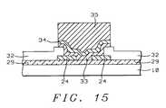
- FIG. 15shows a cross section after photoresist stripping and etching of the layers of UBM and enhanced UBM.
- Contact padshaving dimensions of about 120 ⁇ 120 ⁇ m, are in current practice frequently used as access or input/output contact points during wafer level testing of semiconductor devices. In view of the complexity and density of high performance semiconductor devices, these contact pads will, during a complete cycle of testing, by contacted a number of times. Testing is as a matter of economic necessity performed at high speed which frequently results in landing the test probe on the surface of the contact pad at high speed, resulting in mechanical damage to the surface of the contact pad. In a well controlled testing production line, the distribution of the probe marks (or the damaged surface area of the contact pad) is limited (controlled) to an area in the range of about 60 ⁇ 60 ⁇ m.
- This surfacemay occur in the form of a dent in the surface of the contact pad or may even become severe enough that the surface of the contact pad is broken resulting in the occurrence of burring in the surface of the contact pad.
- probe testingwhich uses bond pads for accessing the devices, must be performed prior to creating wafer solder bumps on the surface of the bond pads, this in order to allow for memory repairs of faulty devices. As indicated above, the testing can cause damage to the surface of the bond pads, creating problems of solder bump and device reliability.
- FIG. 7 ashows a top view of a metal bump structure that is created using current practices
- FIG. 7 bshows a cross section of the metal bump structure using current practices. It is assumed that the views that are shown in FIGS. 7 a and 7 b relate to an aluminum contact pad that has been used as a point of I/O for testing of a device, using a tester probe to contact the aluminum pad.
- FIG. 7 aShown in FIG. 7 a are:
- FIG. 7 bShown in FIG. 7 b are:
- aluminum contact pad 24aligns with a point of electrical contact ( 30 ) that has been provided in the surface of substrate 10
- UBMunder-bump-metal
- a layer of metalsuch as copper or nickel (see FIG. 5) that forms an integral part of the pedestal of the to be created interconnect bump
- layer 32 of passivation materialmay comprise several layers of passivation for applications where additional surface protection is deemed necessary.
- the layer 33 of under bump metalis created overlying the aluminum contact pad 24 .
- the surface of aluminum contact pad 24is not planar and is in many instances disturbed in an unpredictable manner by the tester probe.
- the layer 33 of under bump metaldoes in most cases not fill the damaged surface region 28 of the aluminum pad 24 . This opens the potential for trapping foreign and undesirable materials, such as moisture, a processing gas, a plating solution, solvent and the like, in the unfilled (by the layer 33 of under bump metal) regions in or surrounding the probe mark 28 on the surface of the aluminum pad 24 .
- FIGS. 8 a and 8 bthese figures address the solution that is provided by the invention to the above highlighted problem.
- region 36 on the surface of the aluminum pad 24is shown in the cross section of FIG. 8 b, where it is shown as a region from where the aluminum of the aluminum pad 24 has been removed. With this removal, the probe mark 28 has been removed from the surface of aluminum pad 24 . It is clear from the cross section shown in FIG. 8 b that, should surface irregularities occur in the surface of the aluminum contact pad 24 other than the probe mark 28 , these surface irregularities will also be removed by the removal of the aluminum from the region 36 shown in cross section in FIG. 8 b.
- FIG. 8 bAll elements that are shown in FIG. 8 b have previously been highlighted in FIG. 7 b and are therefore not further explained at this point.
- region 36FIG. 8 b, which will be further highlighted in FIGS. 9 through 11, can be summarized as being performed by depositing a layer of photoresist over the surface of the aluminum pad (typically this implies the deposition of a layer of photoresist over the surface of the entire wafer after wafer level testing has been completed), patterning and etching the layer of photoresist thereby creating openings in the layer of photoresist that align with region 36 for all aluminum pads on the surface of the wafer that have been used as I/O contact points by a tester probe, and removing the aluminum in accordance with the openings that have been created in the layer of photoresist.
- a layer of photoresisttypically this implies the deposition of a layer of photoresist over the surface of the entire wafer after wafer level testing has been completed
- patterning and etching the layer of photoresistthereby creating openings in the layer of photoresist that align with region 36 for all aluminum pads on the surface of the wafer that have been used as I/
- This latter removal (etching) of the aluminumcan be performed using conventional methods of etching aluminum such as plasma enhanced dry etching or wet etching with a H 3 PO 4 solution.
- FIGS. 9 through 15show the processing sequence of the invention, which has as objective to create a metal bump as shown in top view in FIG. 8 a and in cross section in FIG. 8 b.
- FIG. 9shows a cross section of substrate 10 on the surface, the following elements are highlighted:
- dielectric material for layer 29can be used any of the typically applied dielectrics such as silicon dioxide (doped or undoped), silicon oxynitride, parylene or polyimide, spin-on-glass, plasma oxide or LPCVD oxide.
- the material that is used for the deposition of layer 29 of dielectric of the inventionis not limited to the materials indicated above but can include any of the commonly used dielectrics in the art.
- the creation of aluminum pad 24can use conventional methods of metal rf sputtering at a temperature between about 100 and 400 degrees C. and a pressure between about 1 and 100 mTorr using as source aluminum-copper material at a flow rate of between about 10 and 400 sccm to a thickness between about 4000 and 11000 Angstrom.
- the layerAfter a layer of AlCu has been deposited, the layer must be patterned and etched to create the aluminum contact pad 24 . This patterning and etching uses conventional methods of photolithography and patterning and etching.
- the deposited layer of AlCucan be etched using Cl 2 /Ar as an etchant at a temperature between 50 and 200 degrees C., an etchant flow rate of about 20 sccm for the Cl 2 and 1000 sccm for the Ar, a pressure between about 50 mTorr and 10 Torr, a time of the etch between 30 and 200 seconds.
- insulating layerssuch as silicon oxide and oxygen-containing polymers, are deposited using Chemical Vapor Deposition (CVD) technique over the surface of various layers of conducting lines in a semiconductor device or substrate to separate the conductive interconnect lines from each other.
- the insulating layerscan also deposited over patterned layers of interconnecting lines, electrical contact between successive layers of interconnecting lines is established with metal vias created in the insulating layers.
- Electrical contact to the chipis typically established by means of bonding pads or contact pads that form electrical interfaces with patterned levels of interconnecting metal lines. Signal lines and power/ground lines can be connected to the bonding pads or contact pads.
- the bonding pads or contact padsare passivated and electrically insulated by the deposition of a passivation layer over the surface of the bonding pads.
- a passivation layercan contain silicon oxide/silicon nitride (SiO 2 /Si 3 N 4 ) deposited by CVD.
- the passivation layeris patterned and etched to create openings in the passivation layer for the bonding pads or contact pads after which a second and relatively thick passivation layer can be deposited for further insulation and protection of the surface of the chips from moisture and other contaminants and from mechanical damage during assembling of the chips.
- Passivation layercan contain silicon oxide/silicon nitride (SiO 2 /Si 3 N 4 ) deposited by CVD, a passivation layer can be a layer of photosensitive polyimide or can comprise titanium nitride. Another material often used for a passivation layer is phosphorous doped silicon dioxide that is typically deposited over a final layer of aluminum interconnect using a Low Temperature CVD process.
- photosensitive polyimidehas frequently been used for the creation of passivation layers.
- Conventional polyimideshave a number of attractive characteristics for their application in a semiconductor device structure, which have been highlighted above.
- Photosensitive polyimideshave these same characteristics but can, in addition, be patterned like a photoresist mask and can, after patterning and etching, remain on the surface on which it has been deposited to serve as a passivation layer.
- a precursor layeris first deposited by, for example, conventional photoresist spin coating.
- the precursoris, after a low temperature pre-bake, exposed using, for example, a step and repeat projection aligner and Ultra Violet (UV) light as a light source.
- UVUltra Violet
- the portions of the precursor that have been exposed in this mannerare cross-linked, thereby leaving unexposed regions (that are not cross-linked) over the bonding pads.
- the unexposed polyimide precursor layeris dissolved, thereby providing openings over the bonding pads.
- a final step of thermal curingleaves a permanent high quality passivation layer of polyimide over the substrate.
- the preferred material of the invention for the deposition of layer 32 of passivationis Plasma Enhanced silicon nitride (PE Si 3 N 4 ), deposited using PECVD technology at a temperature between about 350 and 450 degrees C. with a pressure of between about 2.0 and 2.8 Torr for the duration between about 8 and 12 seconds.
- PE Si 3 N 4Plasma Enhanced silicon nitride
- Layer 32 of PE Si 3 N 4can be deposited to a thickness between about 200 and 800 Angstrom.
- Layer 32 of PE Si 3 N 4is next patterned and etched to create an opening in the layer 32 that overlays and aligns with the underlying contact pad 24 .
- the etching of layer 32 of passivationcan use Ar/CF 4 as an etchant at a temperature of between about 120 and 160 degrees C. and a pressure of between about 0.30 and 0.40 Torr for a time of between about 33 and 39 seconds using a dry etch process.
- the etching of layer 32 of passivationcan also use He/NF 3 as an etchant at a temperature of between about 80 and 100 degrees C. and a pressure of between about 1.20 and 1.30 Torr for a time of between about 20 and 30 seconds using a dry etch process.
- FIG. 10shows a cross section of the substrate after a layer 37 of photoresist has been deposited over the surface of the layer 32 of passivation, including the opening that has been created in layer 32 .
- the layer 37 of photoresisthas been patterned and developed, creating opening 31 in the layer 37 of photoresist. Opening 31 exposes the probe mark 28 in the surface of aluminum pad 24 .
- Layer 37 of photoresistis typically deposited to a thickness of between about 2000 and 50,000 Angstrom.
- the methods used for the deposition and development of the layer 37 of photoresistuses conventional methods of photolithography.
- Photolithographyis a common approach wherein patterned layers are formed by spinning on a layer of photoresist, projecting light through a photomask with the desired pattern onto the photoresist to expose the photoresist to the pattern, developing the photoresist, washing off the undeveloped photoresist, and plasma etching to clean out the areas where the photoresist has been washed away.
- the exposed resistmay be rendered insoluble (positive-working) and form the pattern, or insoluble (negative working) and be washed away.
- the layer 37 of photoresistwill, after patterning and etching, remain in place in an area above the aluminum pad 24 that surrounds the probe mark 28 in the surface of aluminum pad 24 .
- the deposited layer 37 of photoresistcan, prior to patterning and etching, be cured or pre-baked further hardening the surface of the layer 37 of photoresist.
- Layer 37 of photoresistcan be etched by applying O 2 plasma and then wet stripping by using H 2 SO 4 , H 2 O 2 and NH 4 OH solution.
- Sulfuric acid (H 2 SO 4 ) and mixtures of H 2 SO 4 with other oxidizing agents such as hydrogen peroxide (H 2 O 2 )are widely used in stripping photoresist after the photoresist has been stripped by other means.
- Wafers to be strippedcan be immersed in the mixture at a temperature between about 100 degrees C. and about 150 degrees C. for 5 to 10 minutes and then subjected to a thorough cleaning with deionized water and dried by dry nitrogen.
- Inorganic resist strippers, such as the sulfuric acid mixturesare very effective in the residual free removal of highly postbaked resist. They are more effective than organic strippers and the longer the immersion time, the cleaner and more residue free wafer surface can be obtained.
- the photoresist layer 37can also be partially removed using plasma oxygen ashing and careful wet clean.
- the oxygen plasma ashingis heating the photoresist in a highly oxidized environment, such as an oxygen plasma, thereby converting the photoresist to an easily removed ash.
- the oxygen plasma ashingcan be followed by a native oxide dip for 90 seconds in a 200:1 diluted solution of hydrofluoric acid.
- FIG. 11shows a cross section of the substrate 10 after the aluminum contact pad 24 has been etched in accordance with the opening 31 that has been created in the layer 37 of photoresist.
- This etch of the aluminum padhas created opening 36 in the aluminum pad 24 and has, as is the objective of the invention, removed the probe mark 28 and the regions immediately surrounding the probe mark 28 from the surface of the aluminum pad 24 .
- the etching of the aluminum pad 24 in accordance with opening 31can, as previously stated, use methods of plasma enhanced dry etching or wet etching with a H 3 PO 4 solution. Other methods for the etching of the aluminum pad have previously been highlighted and equally apply at this stage in the process.
- FIG. 11further shows that the patterned layer 37 of photoresist has been removed after opening 36 has been created in the aluminum contact pad 24 . Processing conditions for the removal of the layer of photoresist have previously been indicated and therefore do not need to be repeated at this time.
- FIG. 12shows a cross section after the layer 33 of under bump metal (UBM) has been created aligned with and over the surface of the aluminum contact pad 24 .
- UBMunder bump metal
- a UBM seed layer(not shown in FIG. 12) can be blanket deposited over the surface of the wafer.
- the deposition of a seed layercan further be preceded by the blanket deposition of a barrier layer (not shown in FIG. 12 ), this dependent on the metal that is being used for the metal bump.
- Layer 33 of UBMcan be deposited by vacuum evaporation and may contain multiple layers of metal such as a layer of chrome, followed by a layer of copper, followed by a layer of gold. From the latter it is apparent that layer 33 of UBM may comprise several layers of metal that are successively deposited.
- any of the conventional metallic seed materialscan be used.
- the metallic seed layercan be deposited using a sputter chamber or an Ion Metal Plasma (IMP) chamber at a temperature of between about 0 and 300 degrees C. and a pressure of between about 1 and 100 mTorr, using (for instance) copper or a copper alloy as the source (as highlighted above) at a flow rate of between about 10 and 400 sccm and using argon as an ambient gas.
- IMPIon Metal Plasma
- FIG. 13shows how a layer 39 of photoresist is deposited over the layer 33 of UBM.
- Layer 39 of photoresistis patterned and developed, creating an opening 38 in the layer 39 of photoresist that is slightly wider than the opening of the bonding pad of the to be created solder bump.
- a layer 34 of enhanced UBMtypically of copper or nickel and of a thickness between about 1 and 10 ⁇ m, FIG. 13, is electroplated over the layer 33 of UBM.
- the seed UBM layer 33serves as the common electrode for the electroplating process with the layer of photoresist still being in place.
- the layer 35 of bump metaltypically solder or gold
- the layer 35 of electroplated metalis centered in the opening 38 (FIG. 13) that has been created in the layer 39 of photoresist.
- FIG. 15shows a cross section after the layer 39 (FIG. 14) of photoresist has been removed.
- the layer 33 of UBMhas been etched using the patterned layer 35 of electroplated metal as a mask.
- Another method that can be used for the creation of a metal bumpuses evaporation technology.
- the process of evaporationalso starts with a semiconductor surface wherein a metal point of contact has been provided.
- a layer of passivationis deposited and patterned, creating an opening in the layer of passivation.
- a layer of UBM(this layer may be a composite layer of metal such as chromium followed by copper followed by gold in order to promote (with chromium) improved adhesion and to form a diffusion barrier layer or to prevent oxidation (the gold over the copper)) is formed over the layer of passivation and inside the opening created in the layer of passivation.
- Bump metalis next selectively plated over the deposited layer of UBM and reflowed, in this manner forming a spherically shaped metal bump.
- the cross section that is shown in FIG. 8 bwhich is the desired cross section of the invention, can be achieved by forming the metal bump 35 by reflowing the metal bump layer 35 that is shown in FIG. 15 . If a seed layer (not shown) and or a barrier layer (not shown) have been deposited as part of the processing sequence of the invention, these layers are to be etched, after the layer 39 of photoresist has been removed from the surface and prior to re-flowing the metal bump layer 35 . Conventional methods can be used for these purposes.
- the inventionstarts with a semiconductor surface, a layer of dielectric has been deposited over the semiconductor surface, a contact pad has been provided on the layer of dielectric, the contact pad has served as an Input/Output (I/O) point of contact during semiconductor device testing, the contact pad is assumed to be connected to at least one point of electrical contact provided in or on the surface of the substrate, the at least one point of electrical contact is assumed to be connected to at least one semiconductor device having been provided in or on the surface of the substrate, the contact pad having an exposed surface
- a layer of passivationis deposited over a semiconductor surface including the surface of said contact pad
- the layer of passivationis patterned and etched, creating an opening in the layer of passivation having a first diameter, partially exposing the surface of the contact pad over a surface area of the first diameter, the opening in the layer of passivation being centered with respect to the contact pad
- a first layer of photoresistis deposited over the surface of the layer of passivation, including the opening created in the layer of passivation
- the first layer of photoresistis patterned and etched, creating an opening having a second diameter through the first layer of photoresist, the opening in the first layer of photoresist aligning with and being centered with respect to the contact pad, the second diameter of the opening in the first layer of photoresist being smaller that the first diameter of the opening in the layer of passivation by a measurable amount
- the contact padis etched in accordance with the opening created in the first layer of photoresist, partially exposing the surface of the layer of dielectric deposited over the surface of the substrate
- the patterned layer of first photoresistis removed from the surface of the layer of passivation, including the surface of the etched contact pad
- UBMUnder Bump Metallurgy
- a second layer of photoresistis deposited over the semiconductor surface of the layer of UBM
- the second layer of photoresistis patterned and etched, creating an opening in the second layer of photoresist that is aligned with the contact pad, partially exposing the surface of the layer of UBM
- the exposed surface of the layer of UBMis electroplated with a layer of enhanced UBM
- the layer of enhanced UBMis electroplated with a thick layer of bump metal, partially filling the opening created in the second layer of photoresist
- the patterned and etched second layer of photoresistis removed from above the semiconductor surface
- the layer of UBMis etched using the deposited layer of bump metal as a mask
- the surface of said layer of bump metalis reflowed, forming the metal bump.
Landscapes
- Engineering & Computer Science (AREA)
- Computer Hardware Design (AREA)
- Microelectronics & Electronic Packaging (AREA)
- Power Engineering (AREA)
- Manufacturing & Machinery (AREA)
- Internal Circuitry In Semiconductor Integrated Circuit Devices (AREA)
- Testing Or Measuring Of Semiconductors Or The Like (AREA)
- Wire Bonding (AREA)
Abstract
Description
Claims (66)
Priority Applications (2)
| Application Number | Priority Date | Filing Date | Title |
|---|---|---|---|
| US09/760,909US6426556B1 (en) | 2001-01-16 | 2001-01-16 | Reliable metal bumps on top of I/O pads with test probe marks |
| SG200103355ASG99365A1 (en) | 2001-01-16 | 2001-05-31 | Reliable metal bumps on top of i/o pads with test probe marks |
Applications Claiming Priority (1)
| Application Number | Priority Date | Filing Date | Title |
|---|---|---|---|
| US09/760,909US6426556B1 (en) | 2001-01-16 | 2001-01-16 | Reliable metal bumps on top of I/O pads with test probe marks |
Publications (2)
| Publication Number | Publication Date |
|---|---|
| US6426556B1true US6426556B1 (en) | 2002-07-30 |
| US20020105076A1 US20020105076A1 (en) | 2002-08-08 |
Family
ID=25060537
Family Applications (1)
| Application Number | Title | Priority Date | Filing Date |
|---|---|---|---|
| US09/760,909Expired - LifetimeUS6426556B1 (en) | 2001-01-16 | 2001-01-16 | Reliable metal bumps on top of I/O pads with test probe marks |
Country Status (2)
| Country | Link |
|---|---|
| US (1) | US6426556B1 (en) |
| SG (1) | SG99365A1 (en) |
Cited By (82)
| Publication number | Priority date | Publication date | Assignee | Title |
|---|---|---|---|---|
| WO2002100589A1 (en)* | 2001-06-12 | 2002-12-19 | Applied Materials, Inc. | Integrated solder bump deposition apparatus and method |
| US6509582B1 (en)* | 2002-03-27 | 2003-01-21 | Fairchild Semiconductor Corporation | Semiconductor pad construction enabling pre-bump probing by planarizing the post-sort pad surface |
| US20030080420A1 (en)* | 2001-10-25 | 2003-05-01 | Seiko Epson Corporation | Semiconductor chip and wiring board and manufacturing method of the same, semiconductor wafer, semiconductor device, circuit board, and electronic instrument |
| US20030141593A1 (en)* | 2002-01-25 | 2003-07-31 | Zuniga-Ortiz Edgar R. | Flip-chip without bumps and polymer for board assembly |
| US6636313B2 (en)* | 2002-01-12 | 2003-10-21 | Taiwan Semiconductor Manufacturing Co. Ltd | Method of measuring photoresist and bump misalignment |
| US20030214795A1 (en)* | 2002-05-17 | 2003-11-20 | Fujitsu Limited | Electronic component with bump electrodes, and manufacturing method thereof |
| US20040023433A1 (en)* | 2002-08-02 | 2004-02-05 | Erikson Kenneth R. | High-density interconnection of temperature sensitive electronic devices |
| US20040051116A1 (en)* | 2000-12-20 | 2004-03-18 | Elke Zakel | Contact bump construction for the production of a connector construction for substrate connecting surfaces |
| US6717263B2 (en)* | 2001-10-31 | 2004-04-06 | Sharp Kabushiki Kaisha | Semiconductor device having contact opening smaller than test probe, and manufacturing process and inspecting method thereof |
| US6737353B2 (en)* | 2001-06-19 | 2004-05-18 | Advanced Semiconductor Engineering, Inc. | Semiconductor device having bump electrodes |
| US20040097161A1 (en)* | 2001-03-22 | 2004-05-20 | James Gourlay | Method of creating an electroluminescent device |
| US20040115942A1 (en)* | 2002-12-17 | 2004-06-17 | Date-Gun Lee | Bonding pad of a semiconductor device and formation method thereof |
| US6756294B1 (en)* | 2002-01-30 | 2004-06-29 | Taiwan Semiconductor Manufacturing Company | Method for improving bump reliability for flip chip devices |
| US6815324B2 (en)* | 2001-02-15 | 2004-11-09 | Megic Corporation | Reliable metal bumps on top of I/O pads after removal of test probe marks |
| US20040222522A1 (en)* | 2003-03-13 | 2004-11-11 | Soichi Homma | Semiconductor device and manufacturing method of the same |
| US20040229425A1 (en)* | 2001-03-06 | 2004-11-18 | Katsumi Yamaguchi | Semiconductor device and bump formation method |
| US6821877B1 (en)* | 2003-06-24 | 2004-11-23 | Anam Semiconductor Inc. | Method of fabricating metal interconnection of semiconductor device |
| US6846719B2 (en)* | 2002-02-26 | 2005-01-25 | Advanced Semiconductor Engineering, Inc. | Process for fabricating wafer bumps |
| US20050032349A1 (en)* | 2001-03-05 | 2005-02-10 | Megic Corporation | Low fabrication cost, fine pitch and high reliability solder bump |
| US20060016861A1 (en)* | 2004-07-21 | 2006-01-26 | International Business Machines Corporation | Damascene patterning of barrier layer metal for C4 solder bumps |
| US20060064660A1 (en)* | 2004-09-17 | 2006-03-23 | International Business Machines Corporation | Method and apparatus for depopulating peripheral input/output cells |
| US20060068595A1 (en)* | 2004-09-30 | 2006-03-30 | Frank Seliger | Semiconductor substrate thinning method for manufacturing thinned die |
| KR100574986B1 (en)* | 2004-08-25 | 2006-04-28 | 삼성전자주식회사 | How to form bumps for flip chip connection |
| US20060125094A1 (en)* | 2004-09-20 | 2006-06-15 | Mou-Shiung Lin | Solder interconnect on IC chip |
| US20060211232A1 (en)* | 2005-03-16 | 2006-09-21 | Mei-Jen Liu | Method for Manufacturing Gold Bumps |
| US20060279000A1 (en)* | 2004-01-30 | 2006-12-14 | Ruei-Chih Chang | Pre-solder structure on semiconductor package substrate and method for fabricating the same |
| US20070023483A1 (en)* | 2005-07-27 | 2007-02-01 | Denso Corporation | Packaging method |
| US20070049001A1 (en)* | 2005-08-23 | 2007-03-01 | Advanced Semiconductor Engineering, Inc. | Bumping process and structure thereof |
| US20070063352A1 (en)* | 2005-09-21 | 2007-03-22 | Agere Systems Inc. | Routing under bond pad for the replacement of an interconnect layer |
| US20070063318A1 (en)* | 2005-09-14 | 2007-03-22 | Infineon Technologies Ag | Semiconductor device for bonding connection |
| US20070069394A1 (en)* | 2005-09-27 | 2007-03-29 | Agere Systems Inc. | Solder bump structure for flip chip semiconductor devices and method of manufacture therefore |
| US20070114667A1 (en)* | 2005-11-18 | 2007-05-24 | Lsi Logic Corporation | Alternate pad structures/passivation inegration schemes to reduce or eliminate IMC cracking in post wire bonded dies during Cu/Low-K BEOL processing |
| US20070138635A1 (en)* | 2005-12-20 | 2007-06-21 | Fujitsu Limited | Semiconductor device and manufacturing method of the same |
| US20080029887A1 (en)* | 2006-08-07 | 2008-02-07 | Freescale Semiconductor, Inc. | Electronic device including a conductive stud over a bonding pad region and a process for forming the electronic device |
| US7352001B1 (en) | 2003-07-22 | 2008-04-01 | National Semiconductor Corporation | Method of editing a semiconductor die |
| US20080088019A1 (en)* | 2001-03-05 | 2008-04-17 | Megica Corporation | Structure and manufacturing method of a chip scale package |
| US20080099928A1 (en)* | 2001-09-17 | 2008-05-01 | Megica Corporation | Low fabrication cost, high performance, high reliability chip scale package |
| US20080227237A1 (en)* | 2002-10-25 | 2008-09-18 | Megica Corporation | Method of assembling chips |
| US20090020325A1 (en)* | 2005-03-01 | 2009-01-22 | Robert Hammedinger | Weldable contact and method for the production thereof |
| US20090053887A1 (en)* | 2003-07-23 | 2009-02-26 | Megica Corporation | Wirebond pad for semiconductor chip or wafer |
| US20090098687A1 (en)* | 2007-10-10 | 2009-04-16 | Joze Eura Antol | Integrated circuit package including wire bonds |
| US20090098723A1 (en)* | 2007-10-13 | 2009-04-16 | Wan-Ling Yu | Method Of Forming Metallic Bump On I/O Pad |
| US20090127709A1 (en)* | 2007-11-16 | 2009-05-21 | Rohm Co., Ltd. | Semiconductor device |
| US20090152100A1 (en)* | 2007-12-14 | 2009-06-18 | Ami Semiconductor, Inc. | Thick metal interconnect with metal pad caps at selective sites and process for making the same |
| US20090200675A1 (en)* | 2008-02-11 | 2009-08-13 | Thomas Goebel | Passivated Copper Chip Pads |
| US20100201000A1 (en)* | 2007-10-31 | 2010-08-12 | Agere Systems Inc. | Bond pad support structure for semiconductor device |
| US20110027944A1 (en)* | 2009-07-30 | 2011-02-03 | Taiwan Semiconductor Maufacturing Company, Ltd. | Method of forming electrical connections |
| US20110049705A1 (en)* | 2009-09-01 | 2011-03-03 | Taiwan Semiconductor Manufacturing Company, Ltd. | Self-aligned protection layer for copper post structure |
| US20110101523A1 (en)* | 2009-11-05 | 2011-05-05 | Taiwan Semiconductor Manufacturing Company, Ltd. | Pillar bump with barrier layer |
| US20110215476A1 (en)* | 2002-01-07 | 2011-09-08 | Megica Corporation | Method for fabricating circuit component |
| US20110233761A1 (en)* | 2009-07-30 | 2011-09-29 | Taiwan Semiconductor Manufacturing Company, Ltd. | Cu pillar bump with non-metal sidewall protection structure |
| US20110248406A1 (en)* | 2010-04-09 | 2011-10-13 | Renesas Electronics Corporation | Method of Manufacturing Semiconductor Device |
| US20110266667A1 (en)* | 2010-04-29 | 2011-11-03 | Taiwan Semiconductor Manufacturing Company, Ltd. | Cu pillar bump with non-metal sidewall protection structure |
| US20110291262A1 (en)* | 2010-05-28 | 2011-12-01 | Taiwan Semiconductor Manufacturing Company, Ltd. | Strength of Micro-Bump Joints |
| US8294279B2 (en) | 2005-01-25 | 2012-10-23 | Megica Corporation | Chip package with dam bar restricting flow of underfill |
| US8481418B2 (en) | 2002-05-01 | 2013-07-09 | Megica Corporation | Low fabrication cost, high performance, high reliability chip scale package |
| US8546254B2 (en) | 2010-08-19 | 2013-10-01 | Taiwan Semiconductor Manufacturing Company, Ltd. | Mechanisms for forming copper pillar bumps using patterned anodes |
| US20130307142A1 (en)* | 2012-05-21 | 2013-11-21 | Taiwan Semiconductor Manufacturing Company, Ltd. | Selective solder bump formation on wafer |
| US8610270B2 (en) | 2010-02-09 | 2013-12-17 | Taiwan Semiconductor Manufacturing Company, Ltd. | Semiconductor device and semiconductor assembly with lead-free solder |
| US20140014959A1 (en)* | 2011-12-07 | 2014-01-16 | Taiwan Semiconductor Manufacturing Company, Ltd. | Passivation layer for packaged chip |
| US20140035999A1 (en)* | 2012-08-06 | 2014-02-06 | Canon Kabushiki Kaisha | Liquid ejection head and method for manufacturing liquid ejection head |
| US20150072515A1 (en)* | 2013-09-09 | 2015-03-12 | Rajendra C. Dias | Laser ablation method and recipe for sacrificial material patterning and removal |
| US9018758B2 (en) | 2010-06-02 | 2015-04-28 | Taiwan Semiconductor Manufacturing Company, Ltd. | Cu pillar bump with non-metal sidewall spacer and metal top cap |
| US20150115440A1 (en)* | 2012-08-29 | 2015-04-30 | Panasonic Intellectual Property Management Co., Ltd. | Semiconductor device |
| US20150179596A1 (en)* | 2013-12-24 | 2015-06-25 | Samsung Electro-Mechanics Co., Ltd. | Semiconductor package |
| US20160013162A1 (en)* | 2010-05-20 | 2016-01-14 | Taiwan Semiconductor Manufacturing Company, Ltd. | Substrate Interconnections having Different Sizes |
| JP2016141148A (en)* | 2015-02-05 | 2016-08-08 | キヤノン株式会社 | Manufacturing method for substrate for liquid discharge head |
| US9524945B2 (en) | 2010-05-18 | 2016-12-20 | Taiwan Semiconductor Manufacturing Company, Ltd. | Cu pillar bump with L-shaped non-metal sidewall protection structure |
| US20170069587A1 (en)* | 2012-09-18 | 2017-03-09 | Taiwan Semiconductor Manufacturing Company, Ltd. | Conductive contacts having varying widths and method of manufacturing same |
| CN106505059A (en)* | 2015-09-07 | 2017-03-15 | 矽品精密工业股份有限公司 | Substrate structure |
| US20170207161A1 (en)* | 2016-01-19 | 2017-07-20 | Siliconware Precision Industries Co., Ltd. | Substrate structure and method of manufacturing the same |
| US9761548B1 (en)* | 2016-05-19 | 2017-09-12 | Infineon Technologies Ag | Bond pad structure |
| US9991224B2 (en) | 2012-04-18 | 2018-06-05 | Taiwan Semiconductor Manufacturing Company, Ltd. | Bump-on-trace interconnect having varying widths and methods of forming same |
| US10056345B2 (en) | 2012-04-17 | 2018-08-21 | Taiwan Semiconductor Manufacturing Company, Ltd. | Conical-shaped or tier-shaped pillar connections |
| US10388603B2 (en)* | 2015-10-30 | 2019-08-20 | Murata Manufacturing Co., Ltd. | Thin film element and method for manufacturing the same |
| CN110349870A (en)* | 2018-04-04 | 2019-10-18 | 中芯国际集成电路制造(天津)有限公司 | Wafer stage chip encapsulating structure and preparation method thereof |
| US10566255B2 (en) | 2008-03-31 | 2020-02-18 | Renesas Electronics Corporation | Method of manufacturing semiconductor device |
| US10867944B2 (en)* | 2019-03-27 | 2020-12-15 | Taiwan Semiconductor Manufacturing Company Ltd. | Semiconductor structure and manufacturing method thereof |
| US10893605B2 (en)* | 2019-05-28 | 2021-01-12 | Seagate Technology Llc | Textured test pads for printed circuit board testing |
| CN114093774A (en)* | 2022-01-24 | 2022-02-25 | 四川科尔威光电科技有限公司 | Manufacturing method for presetting gold-tin BUMP based on gallium arsenide wafer electrode |
| WO2023273110A1 (en)* | 2021-06-30 | 2023-01-05 | 颀中科技(苏州)有限公司 | Method for preparing wafer surface dielectric layer, wafer structure, and method for forming bump |
| CN116504748A (en)* | 2022-01-25 | 2023-07-28 | 意法半导体有限公司 | Thick bond pad structure for wire bond stress reduction |
Families Citing this family (11)
| Publication number | Priority date | Publication date | Assignee | Title |
|---|---|---|---|---|
| TW517334B (en)* | 2000-12-08 | 2003-01-11 | Nec Corp | Method of forming barrier layers for solder bumps |
| US6696356B2 (en)* | 2001-12-31 | 2004-02-24 | Taiwan Semiconductor Manufacturing Co., Ltd. | Method of making a bump on a substrate without ribbon residue |
| US20040099959A1 (en)* | 2002-11-22 | 2004-05-27 | Hannstar Display Corp. | Conductive bump structure |
| TWI230425B (en)* | 2004-02-06 | 2005-04-01 | South Epitaxy Corp | Bumping process for light emitting diode |
| CN101006347A (en)* | 2004-08-26 | 2007-07-25 | Sv探针私人有限公司 | Stacked tip cantilever electrical connector |
| EP1790008A1 (en)* | 2004-08-31 | 2007-05-30 | Koninklijke Philips Electronics N.V. | Chip comprising at least one test contact configuration |
| JP2006119024A (en)* | 2004-10-22 | 2006-05-11 | Tokyo Electron Ltd | Probe and its manufacturing method |
| US20060226442A1 (en)* | 2005-04-07 | 2006-10-12 | An-Ping Zhang | GaN-based high electron mobility transistor and method for making the same |
| US7682959B2 (en)* | 2007-03-21 | 2010-03-23 | Stats Chippac, Ltd. | Method of forming solder bump on high topography plated Cu |
| US8373282B2 (en)* | 2011-06-16 | 2013-02-12 | Taiwan Semiconductor Manufacturing Company, Ltd. | Wafer level chip scale package with reduced stress on solder balls |
| US9935024B2 (en) | 2016-04-28 | 2018-04-03 | Taiwan Semiconductor Manufacturing Co., Ltd. | Method for forming semiconductor structure |
Citations (7)
| Publication number | Priority date | Publication date | Assignee | Title |
|---|---|---|---|---|
| US5554940A (en) | 1994-07-05 | 1996-09-10 | Motorola, Inc. | Bumped semiconductor device and method for probing the same |
| US5656858A (en)* | 1994-10-19 | 1997-08-12 | Nippondenso Co., Ltd. | Semiconductor device with bump structure |
| US5747881A (en)* | 1995-02-01 | 1998-05-05 | Kabushiki Kaisha Toshiba | Semiconductor device, method of fabricating the same and copper leads |
| US5756370A (en) | 1996-02-08 | 1998-05-26 | Micron Technology, Inc. | Compliant contact system with alignment structure for testing unpackaged semiconductor dice |
| JPH11204525A (en)* | 1998-01-14 | 1999-07-30 | Seiko Epson Corp | Method for manufacturing semiconductor device |
| US6157079A (en)* | 1997-11-10 | 2000-12-05 | Citizen Watch Co., Ltd | Semiconductor device with a bump including a bump electrode film covering a projecting photoresist |
| US6162652A (en) | 1997-12-31 | 2000-12-19 | Intel Corporation | Process for sort testing C4 bumped wafers |
- 2001
- 2001-01-16USUS09/760,909patent/US6426556B1/ennot_activeExpired - Lifetime
- 2001-05-31SGSG200103355Apatent/SG99365A1/enunknown
Patent Citations (7)
| Publication number | Priority date | Publication date | Assignee | Title |
|---|---|---|---|---|
| US5554940A (en) | 1994-07-05 | 1996-09-10 | Motorola, Inc. | Bumped semiconductor device and method for probing the same |
| US5656858A (en)* | 1994-10-19 | 1997-08-12 | Nippondenso Co., Ltd. | Semiconductor device with bump structure |
| US5747881A (en)* | 1995-02-01 | 1998-05-05 | Kabushiki Kaisha Toshiba | Semiconductor device, method of fabricating the same and copper leads |
| US5756370A (en) | 1996-02-08 | 1998-05-26 | Micron Technology, Inc. | Compliant contact system with alignment structure for testing unpackaged semiconductor dice |
| US6157079A (en)* | 1997-11-10 | 2000-12-05 | Citizen Watch Co., Ltd | Semiconductor device with a bump including a bump electrode film covering a projecting photoresist |
| US6162652A (en) | 1997-12-31 | 2000-12-19 | Intel Corporation | Process for sort testing C4 bumped wafers |
| JPH11204525A (en)* | 1998-01-14 | 1999-07-30 | Seiko Epson Corp | Method for manufacturing semiconductor device |
Cited By (177)
| Publication number | Priority date | Publication date | Assignee | Title |
|---|---|---|---|---|
| US20040051116A1 (en)* | 2000-12-20 | 2004-03-18 | Elke Zakel | Contact bump construction for the production of a connector construction for substrate connecting surfaces |
| US7007834B2 (en)* | 2000-12-20 | 2006-03-07 | PAC Tech—Packaging Technologies GmbH | Contact bump construction for the production of a connector construction for substrate connecting surfaces |
| US20050070085A1 (en)* | 2001-02-15 | 2005-03-31 | Megic Corporation | Reliable metal bumps on top of I/O pads after removal of test probe marks |
| US20080284016A1 (en)* | 2001-02-15 | 2008-11-20 | Megica Corporation | Reliable metal bumps on top of I/O pads after removal of test probe marks |
| US7465653B2 (en)* | 2001-02-15 | 2008-12-16 | Megica Corporation | Reliable metal bumps on top of I/O pads after removal of test probe marks |
| US8901733B2 (en) | 2001-02-15 | 2014-12-02 | Qualcomm Incorporated | Reliable metal bumps on top of I/O pads after removal of test probe marks |
| US6815324B2 (en)* | 2001-02-15 | 2004-11-09 | Megic Corporation | Reliable metal bumps on top of I/O pads after removal of test probe marks |
| US20080088019A1 (en)* | 2001-03-05 | 2008-04-17 | Megica Corporation | Structure and manufacturing method of a chip scale package |
| US20050032349A1 (en)* | 2001-03-05 | 2005-02-10 | Megic Corporation | Low fabrication cost, fine pitch and high reliability solder bump |
| US8368213B2 (en) | 2001-03-05 | 2013-02-05 | Megica Corporation | Low fabrication cost, fine pitch and high reliability solder bump |
| US8072070B2 (en) | 2001-03-05 | 2011-12-06 | Megica Corporation | Low fabrication cost, fine pitch and high reliability solder bump |
| US20040229425A1 (en)* | 2001-03-06 | 2004-11-18 | Katsumi Yamaguchi | Semiconductor device and bump formation method |
| US7595588B2 (en)* | 2001-03-22 | 2009-09-29 | Microemissive Displays Limited | Electroluminescent device and method of making same |
| US20040097161A1 (en)* | 2001-03-22 | 2004-05-20 | James Gourlay | Method of creating an electroluminescent device |
| WO2002100589A1 (en)* | 2001-06-12 | 2002-12-19 | Applied Materials, Inc. | Integrated solder bump deposition apparatus and method |
| US6572010B2 (en)* | 2001-06-12 | 2003-06-03 | Applied Materials Inc. | Integrated solder bump deposition apparatus and method |
| US6737353B2 (en)* | 2001-06-19 | 2004-05-18 | Advanced Semiconductor Engineering, Inc. | Semiconductor device having bump electrodes |
| US9369175B2 (en) | 2001-09-17 | 2016-06-14 | Qualcomm Incorporated | Low fabrication cost, high performance, high reliability chip scale package |
| US20100038803A9 (en)* | 2001-09-17 | 2010-02-18 | Megica Corporation | Low fabrication cost, high performance, high reliability chip scale package |
| US20080099928A1 (en)* | 2001-09-17 | 2008-05-01 | Megica Corporation | Low fabrication cost, high performance, high reliability chip scale package |
| US8178967B2 (en) | 2001-09-17 | 2012-05-15 | Megica Corporation | Low fabrication cost, high performance, high reliability chip scale package |
| US20030080420A1 (en)* | 2001-10-25 | 2003-05-01 | Seiko Epson Corporation | Semiconductor chip and wiring board and manufacturing method of the same, semiconductor wafer, semiconductor device, circuit board, and electronic instrument |
| US6924553B2 (en)* | 2001-10-25 | 2005-08-02 | Seiko Epson Corporation | Semiconductor chip and wiring board with bumps formed on pads/land and on passivation/insulation film and manufacturing method of the same |
| US6717263B2 (en)* | 2001-10-31 | 2004-04-06 | Sharp Kabushiki Kaisha | Semiconductor device having contact opening smaller than test probe, and manufacturing process and inspecting method thereof |
| US20110215476A1 (en)* | 2002-01-07 | 2011-09-08 | Megica Corporation | Method for fabricating circuit component |
| US8461679B2 (en)* | 2002-01-07 | 2013-06-11 | Megica Corporation | Method for fabricating circuit component |
| US8890336B2 (en) | 2002-01-07 | 2014-11-18 | Qualcomm Incorporated | Cylindrical bonding structure and method of manufacture |
| US6636313B2 (en)* | 2002-01-12 | 2003-10-21 | Taiwan Semiconductor Manufacturing Co. Ltd | Method of measuring photoresist and bump misalignment |
| US6914332B2 (en)* | 2002-01-25 | 2005-07-05 | Texas Instruments Incorporated | Flip-chip without bumps and polymer for board assembly |
| US20030141593A1 (en)* | 2002-01-25 | 2003-07-31 | Zuniga-Ortiz Edgar R. | Flip-chip without bumps and polymer for board assembly |
| US6756294B1 (en)* | 2002-01-30 | 2004-06-29 | Taiwan Semiconductor Manufacturing Company | Method for improving bump reliability for flip chip devices |
| US6846719B2 (en)* | 2002-02-26 | 2005-01-25 | Advanced Semiconductor Engineering, Inc. | Process for fabricating wafer bumps |
| US6509582B1 (en)* | 2002-03-27 | 2003-01-21 | Fairchild Semiconductor Corporation | Semiconductor pad construction enabling pre-bump probing by planarizing the post-sort pad surface |
| US8481418B2 (en) | 2002-05-01 | 2013-07-09 | Megica Corporation | Low fabrication cost, high performance, high reliability chip scale package |
| US20030214795A1 (en)* | 2002-05-17 | 2003-11-20 | Fujitsu Limited | Electronic component with bump electrodes, and manufacturing method thereof |
| US7189927B2 (en)* | 2002-05-17 | 2007-03-13 | Fujitsu Limited | Electronic component with bump electrodes, and manufacturing method thereof |
| US20040023433A1 (en)* | 2002-08-02 | 2004-02-05 | Erikson Kenneth R. | High-density interconnection of temperature sensitive electronic devices |
| WO2004013698A1 (en)* | 2002-08-02 | 2004-02-12 | Bae Systems Information And Electronic Systems Integration Inc. | High-density interconnection of temperature sensitive electronic devices |
| US6716669B2 (en) | 2002-08-02 | 2004-04-06 | Bae Systems Information And Electronic Systems Integration Inc | High-density interconnection of temperature sensitive electronic devices |
| US20080227237A1 (en)* | 2002-10-25 | 2008-09-18 | Megica Corporation | Method of assembling chips |
| US8421222B2 (en) | 2002-10-25 | 2013-04-16 | Megica Corporation | Chip package having a chip combined with a substrate via a copper pillar |
| US8021921B2 (en) | 2002-10-25 | 2011-09-20 | Megica Corporation | Method of joining chips utilizing copper pillar |
| US20040115942A1 (en)* | 2002-12-17 | 2004-06-17 | Date-Gun Lee | Bonding pad of a semiconductor device and formation method thereof |
| US6995082B2 (en)* | 2002-12-17 | 2006-02-07 | Dongbuanam Semiconductor, Inc. | Bonding pad of a semiconductor device and formation method thereof |
| US20040222522A1 (en)* | 2003-03-13 | 2004-11-11 | Soichi Homma | Semiconductor device and manufacturing method of the same |
| US6821877B1 (en)* | 2003-06-24 | 2004-11-23 | Anam Semiconductor Inc. | Method of fabricating metal interconnection of semiconductor device |
| US7352001B1 (en) | 2003-07-22 | 2008-04-01 | National Semiconductor Corporation | Method of editing a semiconductor die |
| US20090053887A1 (en)* | 2003-07-23 | 2009-02-26 | Megica Corporation | Wirebond pad for semiconductor chip or wafer |
| US8187965B2 (en) | 2003-07-23 | 2012-05-29 | Megica Corporation | Wirebond pad for semiconductor chip or wafer |
| US20060279000A1 (en)* | 2004-01-30 | 2006-12-14 | Ruei-Chih Chang | Pre-solder structure on semiconductor package substrate and method for fabricating the same |
| US7541272B2 (en) | 2004-07-21 | 2009-06-02 | International Business Machines Corporation | Damascene patterning of barrier layer metal for C4 solder bumps |
| US20070111502A1 (en)* | 2004-07-21 | 2007-05-17 | International Business Machines Corporation | Damascene patterning of barrier layer metal for c4 solder bumps |
| US7176583B2 (en) | 2004-07-21 | 2007-02-13 | International Business Machines Corporation | Damascene patterning of barrier layer metal for C4 solder bumps |
| US20060016861A1 (en)* | 2004-07-21 | 2006-01-26 | International Business Machines Corporation | Damascene patterning of barrier layer metal for C4 solder bumps |
| KR100574986B1 (en)* | 2004-08-25 | 2006-04-28 | 삼성전자주식회사 | How to form bumps for flip chip connection |
| US7194707B2 (en) | 2004-09-17 | 2007-03-20 | International Business Machines Corporation | Method and apparatus for depopulating peripheral input/output cells |
| US20060064660A1 (en)* | 2004-09-17 | 2006-03-23 | International Business Machines Corporation | Method and apparatus for depopulating peripheral input/output cells |
| US8067837B2 (en) | 2004-09-20 | 2011-11-29 | Megica Corporation | Metallization structure over passivation layer for IC chip |
| US8742582B2 (en) | 2004-09-20 | 2014-06-03 | Megit Acquisition Corp. | Solder interconnect on IC chip |
| US20060125094A1 (en)* | 2004-09-20 | 2006-06-15 | Mou-Shiung Lin | Solder interconnect on IC chip |
| US20060068595A1 (en)* | 2004-09-30 | 2006-03-30 | Frank Seliger | Semiconductor substrate thinning method for manufacturing thinned die |
| US7375032B2 (en)* | 2004-09-30 | 2008-05-20 | Advanced Micro Devices, Inc. | Semiconductor substrate thinning method for manufacturing thinned die |
| US8294279B2 (en) | 2005-01-25 | 2012-10-23 | Megica Corporation | Chip package with dam bar restricting flow of underfill |
| US20090020325A1 (en)* | 2005-03-01 | 2009-01-22 | Robert Hammedinger | Weldable contact and method for the production thereof |
| DE102005009358B4 (en)* | 2005-03-01 | 2021-02-04 | Snaptrack, Inc. | Solderable Contact and Method of Manufacture |
| US8456022B2 (en)* | 2005-03-01 | 2013-06-04 | Epcos Ag | Weldable contact and method for the production thereof |
| US20060211232A1 (en)* | 2005-03-16 | 2006-09-21 | Mei-Jen Liu | Method for Manufacturing Gold Bumps |
| US7470996B2 (en)* | 2005-07-27 | 2008-12-30 | Denso Corporation | Packaging method |
| US20070023483A1 (en)* | 2005-07-27 | 2007-02-01 | Denso Corporation | Packaging method |
| US7651937B2 (en)* | 2005-08-23 | 2010-01-26 | Advanced Semiconductor Engineering, Inc. | Bumping process and structure thereof |
| US20070049001A1 (en)* | 2005-08-23 | 2007-03-01 | Advanced Semiconductor Engineering, Inc. | Bumping process and structure thereof |
| US9059182B2 (en)* | 2005-09-14 | 2015-06-16 | Infineon Technologies Ag | Method for producing bonding connection of semiconductor device |
| US20070063318A1 (en)* | 2005-09-14 | 2007-03-22 | Infineon Technologies Ag | Semiconductor device for bonding connection |
| US8319343B2 (en) | 2005-09-21 | 2012-11-27 | Agere Systems Llc | Routing under bond pad for the replacement of an interconnect layer |
| US20070063352A1 (en)* | 2005-09-21 | 2007-03-22 | Agere Systems Inc. | Routing under bond pad for the replacement of an interconnect layer |
| US8507317B2 (en) | 2005-09-27 | 2013-08-13 | Agere Systems Llc | Solder bump structure for flip chip semiconductor devices and method of manufacturing therefore |
| US7952206B2 (en)* | 2005-09-27 | 2011-05-31 | Agere Systems Inc. | Solder bump structure for flip chip semiconductor devices and method of manufacture therefore |
| US20110195544A1 (en)* | 2005-09-27 | 2011-08-11 | Bachman Mark A | Solder bump structure for flip chip semiconductor devices and method of manufacture therefor |
| US20070069394A1 (en)* | 2005-09-27 | 2007-03-29 | Agere Systems Inc. | Solder bump structure for flip chip semiconductor devices and method of manufacture therefore |
| US8552560B2 (en) | 2005-11-18 | 2013-10-08 | Lsi Corporation | Alternate pad structures/passivation inegration schemes to reduce or eliminate IMC cracking in post wire bonded dies during Cu/Low-K BEOL processing |
| US20070114667A1 (en)* | 2005-11-18 | 2007-05-24 | Lsi Logic Corporation | Alternate pad structures/passivation inegration schemes to reduce or eliminate IMC cracking in post wire bonded dies during Cu/Low-K BEOL processing |
| US20070138635A1 (en)* | 2005-12-20 | 2007-06-21 | Fujitsu Limited | Semiconductor device and manufacturing method of the same |
| US20080293234A1 (en)* | 2005-12-20 | 2008-11-27 | Fujitsu Limited | Semiconductor device and manufacturing method of the same |
| CN1988143B (en)* | 2005-12-20 | 2011-07-27 | 富士通半导体股份有限公司 | Semiconductor device and manufacturing method of the same |
| US7417326B2 (en)* | 2005-12-20 | 2008-08-26 | Fujitsu Limited | Semiconductor device and manufacturing method of the same |
| US8420522B2 (en) | 2005-12-20 | 2013-04-16 | Fujitsu Semiconductor Limited | Semiconductor device and manufacturing method of the same |
| US20110027984A1 (en)* | 2006-08-07 | 2011-02-03 | Freescale Semiconductor, Inc. | Process of forming an electronic device including a conductive stud over a bonding pad region |
| US20080029887A1 (en)* | 2006-08-07 | 2008-02-07 | Freescale Semiconductor, Inc. | Electronic device including a conductive stud over a bonding pad region and a process for forming the electronic device |
| US8530346B2 (en) | 2006-08-07 | 2013-09-10 | Freescale Semiconductor, Inc. | Process of forming an electronic device including a conductive stud over a bonding pad region |
| US7812448B2 (en)* | 2006-08-07 | 2010-10-12 | Freescale Semiconductor, Inc. | Electronic device including a conductive stud over a bonding pad region |
| US20090098687A1 (en)* | 2007-10-10 | 2009-04-16 | Joze Eura Antol | Integrated circuit package including wire bonds |
| US7888257B2 (en) | 2007-10-10 | 2011-02-15 | Agere Systems Inc. | Integrated circuit package including wire bonds |
| US20090098723A1 (en)* | 2007-10-13 | 2009-04-16 | Wan-Ling Yu | Method Of Forming Metallic Bump On I/O Pad |
| US7713860B2 (en)* | 2007-10-13 | 2010-05-11 | Wan-Ling Yu | Method of forming metallic bump on I/O pad |
| US20100201000A1 (en)* | 2007-10-31 | 2010-08-12 | Agere Systems Inc. | Bond pad support structure for semiconductor device |
| US8183698B2 (en) | 2007-10-31 | 2012-05-22 | Agere Systems Inc. | Bond pad support structure for semiconductor device |
| US20090127709A1 (en)* | 2007-11-16 | 2009-05-21 | Rohm Co., Ltd. | Semiconductor device |
| US9941231B2 (en) | 2007-11-16 | 2018-04-10 | Rohm Co., Ltd. | Semiconductor device |
| US9607957B2 (en) | 2007-11-16 | 2017-03-28 | Rohm Co., Ltd. | Semiconductor device |
| US9035455B2 (en)* | 2007-11-16 | 2015-05-19 | Rohm Co., Ltd. | Semiconductor device |
| US9437544B2 (en) | 2007-11-16 | 2016-09-06 | Rohm Co., Ltd. | Semiconductor device |
| US7947592B2 (en)* | 2007-12-14 | 2011-05-24 | Semiconductor Components Industries, Llc | Thick metal interconnect with metal pad caps at selective sites and process for making the same |
| US20090152100A1 (en)* | 2007-12-14 | 2009-06-18 | Ami Semiconductor, Inc. | Thick metal interconnect with metal pad caps at selective sites and process for making the same |
| US9373596B2 (en) | 2008-02-11 | 2016-06-21 | Infineon Technologies Ag | Passivated copper chip pads |
| US20090200675A1 (en)* | 2008-02-11 | 2009-08-13 | Thomas Goebel | Passivated Copper Chip Pads |
| US8822324B2 (en) | 2008-02-11 | 2014-09-02 | Infineon Technologies Ag | Passivated copper chip pads |
| US10566255B2 (en) | 2008-03-31 | 2020-02-18 | Renesas Electronics Corporation | Method of manufacturing semiconductor device |
| US20110233761A1 (en)* | 2009-07-30 | 2011-09-29 | Taiwan Semiconductor Manufacturing Company, Ltd. | Cu pillar bump with non-metal sidewall protection structure |
| US8841766B2 (en)* | 2009-07-30 | 2014-09-23 | Taiwan Semiconductor Manufacturing Company, Ltd. | Cu pillar bump with non-metal sidewall protection structure |
| US8377816B2 (en) | 2009-07-30 | 2013-02-19 | Taiwan Semiconductor Manufacturing Company, Ltd. | Method of forming electrical connections |
| US20110027944A1 (en)* | 2009-07-30 | 2011-02-03 | Taiwan Semiconductor Maufacturing Company, Ltd. | Method of forming electrical connections |
| US20110049705A1 (en)* | 2009-09-01 | 2011-03-03 | Taiwan Semiconductor Manufacturing Company, Ltd. | Self-aligned protection layer for copper post structure |
| US8623755B2 (en) | 2009-09-01 | 2014-01-07 | Taiwan Semiconductor Manufacturing Company, Ltd. | Self-aligned protection layer for copper post structure |
| US8324738B2 (en) | 2009-09-01 | 2012-12-04 | Taiwan Semiconductor Manufacturing Company, Ltd. | Self-aligned protection layer for copper post structure |
| US9214428B2 (en) | 2009-09-01 | 2015-12-15 | Taiwan Semiconductor Manufacturing Company, Ltd. | Self-aligned protection layer for copper post structure |
| US8501616B2 (en) | 2009-09-01 | 2013-08-06 | Taiwan Semiconductor Manufacturing Company, Ltd. | Self-aligned protection layer for copper post structure |
| US8659155B2 (en) | 2009-11-05 | 2014-02-25 | Taiwan Semiconductor Manufacturing Company, Ltd. | Mechanisms for forming copper pillar bumps |
| US20110101523A1 (en)* | 2009-11-05 | 2011-05-05 | Taiwan Semiconductor Manufacturing Company, Ltd. | Pillar bump with barrier layer |
| US8610270B2 (en) | 2010-02-09 | 2013-12-17 | Taiwan Semiconductor Manufacturing Company, Ltd. | Semiconductor device and semiconductor assembly with lead-free solder |
| US8952534B2 (en) | 2010-02-09 | 2015-02-10 | Taiwan Semiconductor Manufacturing Company, Ltd. | Semiconductor device and semiconductor assembly with lead-free solder |
| US9136167B2 (en) | 2010-03-24 | 2015-09-15 | Taiwan Semiconductor Manufacturing Company, Ltd. | Method of making a pillar structure having a non-metal sidewall protection structure |
| US11257714B2 (en) | 2010-03-24 | 2022-02-22 | Taiwan Semiconductor Manufacturing Company, Ltd. | Method of making a pillar structure having a non-metal sidewall protection structure and integrated circuit including the same |
| US8338288B2 (en)* | 2010-04-09 | 2012-12-25 | Renesas Electronics Corporation | Method of manufacturing semiconductor device |
| US8587135B2 (en) | 2010-04-09 | 2013-11-19 | Renesas Electronics Corporation | Semiconductor device having electrode/film opening edge spacing smaller than bonding pad/electrode edge spacing |
| US20110248406A1 (en)* | 2010-04-09 | 2011-10-13 | Renesas Electronics Corporation | Method of Manufacturing Semiconductor Device |
| US20110266667A1 (en)* | 2010-04-29 | 2011-11-03 | Taiwan Semiconductor Manufacturing Company, Ltd. | Cu pillar bump with non-metal sidewall protection structure |
| US9287171B2 (en) | 2010-04-29 | 2016-03-15 | Taiwan Semiconductor Manufacturing Company, Ltd. | Method of making a conductive pillar bump with non-metal sidewall protection structure |
| US8823167B2 (en) | 2010-04-29 | 2014-09-02 | Taiwan Semiconductor Manufacturing Company, Ltd. | Copper pillar bump with non-metal sidewall protection structure and method of making the same |
| US8441124B2 (en)* | 2010-04-29 | 2013-05-14 | Taiwan Semiconductor Manufacturing Company, Ltd. | Cu pillar bump with non-metal sidewall protection structure |
| US10163837B2 (en) | 2010-05-18 | 2018-12-25 | Taiwan Semiconductor Manufacturing Company, Ltd. | Cu pillar bump with L-shaped non-metal sidewall protection structure |
| US9524945B2 (en) | 2010-05-18 | 2016-12-20 | Taiwan Semiconductor Manufacturing Company, Ltd. | Cu pillar bump with L-shaped non-metal sidewall protection structure |
| US9773755B2 (en)* | 2010-05-20 | 2017-09-26 | Taiwan Semiconductor Manufacturing Company, Ltd. | Substrate interconnections having different sizes |
| US20160013162A1 (en)* | 2010-05-20 | 2016-01-14 | Taiwan Semiconductor Manufacturing Company, Ltd. | Substrate Interconnections having Different Sizes |
| US20110291262A1 (en)* | 2010-05-28 | 2011-12-01 | Taiwan Semiconductor Manufacturing Company, Ltd. | Strength of Micro-Bump Joints |
| US9768138B2 (en) | 2010-05-28 | 2017-09-19 | Taiwan Semiconductor Manufacturing Company, Ltd. | Improving the strength of micro-bump joints |
| US8901736B2 (en)* | 2010-05-28 | 2014-12-02 | Taiwan Semiconductor Manufacturing Company, Ltd. | Strength of micro-bump joints |
| US9018758B2 (en) | 2010-06-02 | 2015-04-28 | Taiwan Semiconductor Manufacturing Company, Ltd. | Cu pillar bump with non-metal sidewall spacer and metal top cap |
| US9685372B2 (en) | 2010-06-02 | 2017-06-20 | Taiwan Semiconductor Manufacturing Company, Ltd. | Method of forming Cu pillar bump with non-metal sidewall spacer and metal top cap |
| US8581401B2 (en) | 2010-08-19 | 2013-11-12 | Taiwan Semiconductor Manufacturing Company, Ltd. | Mechanisms for forming copper pillar bumps using patterned anodes |
| US8546254B2 (en) | 2010-08-19 | 2013-10-01 | Taiwan Semiconductor Manufacturing Company, Ltd. | Mechanisms for forming copper pillar bumps using patterned anodes |
| US9570366B2 (en)* | 2011-12-07 | 2017-02-14 | Taiwan Semiconductor Manufacturing Company, Ltd. | Passivation layer for packaged chip |
| US20140014959A1 (en)* | 2011-12-07 | 2014-01-16 | Taiwan Semiconductor Manufacturing Company, Ltd. | Passivation layer for packaged chip |
| US10056345B2 (en) | 2012-04-17 | 2018-08-21 | Taiwan Semiconductor Manufacturing Company, Ltd. | Conical-shaped or tier-shaped pillar connections |
| US11315896B2 (en) | 2012-04-17 | 2022-04-26 | Taiwan Semiconductor Manufacturing Company, Ltd. | Conical-shaped or tier-shaped pillar connections |
| US10847493B2 (en) | 2012-04-18 | 2020-11-24 | Taiwan Semiconductor Manufacturing, Ltd. | Bump-on-trace interconnect |
| US10510710B2 (en) | 2012-04-18 | 2019-12-17 | Taiwan Semiconductor Manufacturing Company, Ltd. | Bump-on-trace interconnect |
| US11682651B2 (en) | 2012-04-18 | 2023-06-20 | Taiwan Semiconductor Manufacturing Company | Bump-on-trace interconnect |
| US9991224B2 (en) | 2012-04-18 | 2018-06-05 | Taiwan Semiconductor Manufacturing Company, Ltd. | Bump-on-trace interconnect having varying widths and methods of forming same |
| US20130307142A1 (en)* | 2012-05-21 | 2013-11-21 | Taiwan Semiconductor Manufacturing Company, Ltd. | Selective solder bump formation on wafer |
| US9941176B2 (en)* | 2012-05-21 | 2018-04-10 | Taiwan Semiconductor Manufacturing Company, Ltd. | Selective solder bump formation on wafer |
| US20140035999A1 (en)* | 2012-08-06 | 2014-02-06 | Canon Kabushiki Kaisha | Liquid ejection head and method for manufacturing liquid ejection head |
| US9174439B2 (en)* | 2012-08-06 | 2015-11-03 | Canon Kabushiki Kaisha | Liquid ejection head and method for manufacturing liquid ejection head |
| US20150115440A1 (en)* | 2012-08-29 | 2015-04-30 | Panasonic Intellectual Property Management Co., Ltd. | Semiconductor device |
| US9520381B2 (en)* | 2012-08-29 | 2016-12-13 | Panasonic Intellectual Property Management Co., Ltd. | Semiconductor device for use in flip-chip bonding, which reduces lateral displacement |
| US10319691B2 (en) | 2012-09-18 | 2019-06-11 | Taiwan Semiconductor Manufacturing Company | Solderless interconnection structure and method of forming same |
| US9966346B2 (en) | 2012-09-18 | 2018-05-08 | Taiwan Semiconductor Manufacturing Company | Bump structure and method of forming same |
| US9953939B2 (en)* | 2012-09-18 | 2018-04-24 | Taiwan Semiconductor Manufacturing Company, Ltd. | Conductive contacts having varying widths and method of manufacturing same |
| US11961810B2 (en) | 2012-09-18 | 2024-04-16 | Taiwan Semiconductor Manufacturing Company | Solderless interconnection structure and method of forming same |
| US20170069587A1 (en)* | 2012-09-18 | 2017-03-09 | Taiwan Semiconductor Manufacturing Company, Ltd. | Conductive contacts having varying widths and method of manufacturing same |
| US11043462B2 (en) | 2012-09-18 | 2021-06-22 | Taiwan Semiconductor Manufacturing Company | Solderless interconnection structure and method of forming same |
| US10008459B2 (en) | 2012-09-18 | 2018-06-26 | Taiwan Semiconductor Manufacturing Company | Structures having a tapering curved profile and methods of making same |
| US20150072515A1 (en)* | 2013-09-09 | 2015-03-12 | Rajendra C. Dias | Laser ablation method and recipe for sacrificial material patterning and removal |
| US20150179596A1 (en)* | 2013-12-24 | 2015-06-25 | Samsung Electro-Mechanics Co., Ltd. | Semiconductor package |
| JP2016141148A (en)* | 2015-02-05 | 2016-08-08 | キヤノン株式会社 | Manufacturing method for substrate for liquid discharge head |
| CN106505059A (en)* | 2015-09-07 | 2017-03-15 | 矽品精密工业股份有限公司 | Substrate structure |
| CN106505059B (en)* | 2015-09-07 | 2019-11-08 | 矽品精密工业股份有限公司 | Substrate structure |
| US10388603B2 (en)* | 2015-10-30 | 2019-08-20 | Murata Manufacturing Co., Ltd. | Thin film element and method for manufacturing the same |
| US11973014B2 (en)* | 2016-01-19 | 2024-04-30 | Siliconware Precision Industries Co., Ltd. | Method of manufacturing substrate structure with filling material formed in concave portion |
| US20170207161A1 (en)* | 2016-01-19 | 2017-07-20 | Siliconware Precision Industries Co., Ltd. | Substrate structure and method of manufacturing the same |
| US10522453B2 (en)* | 2016-01-19 | 2019-12-31 | Siliconware Precision Industries Co., Ltd. | Substrate structure with filling material formed in concave portion |
| US9761548B1 (en)* | 2016-05-19 | 2017-09-12 | Infineon Technologies Ag | Bond pad structure |
| CN110349870A (en)* | 2018-04-04 | 2019-10-18 | 中芯国际集成电路制造(天津)有限公司 | Wafer stage chip encapsulating structure and preparation method thereof |
| US10867944B2 (en)* | 2019-03-27 | 2020-12-15 | Taiwan Semiconductor Manufacturing Company Ltd. | Semiconductor structure and manufacturing method thereof |
| US10893605B2 (en)* | 2019-05-28 | 2021-01-12 | Seagate Technology Llc | Textured test pads for printed circuit board testing |
| WO2023273110A1 (en)* | 2021-06-30 | 2023-01-05 | 颀中科技(苏州)有限公司 | Method for preparing wafer surface dielectric layer, wafer structure, and method for forming bump |
| CN114093774A (en)* | 2022-01-24 | 2022-02-25 | 四川科尔威光电科技有限公司 | Manufacturing method for presetting gold-tin BUMP based on gallium arsenide wafer electrode |
| CN116504748A (en)* | 2022-01-25 | 2023-07-28 | 意法半导体有限公司 | Thick bond pad structure for wire bond stress reduction |
Also Published As
| Publication number | Publication date |
|---|---|
| US20020105076A1 (en) | 2002-08-08 |
| SG99365A1 (en) | 2003-10-27 |
Similar Documents
| Publication | Publication Date | Title |
|---|---|---|
| US6426556B1 (en) | Reliable metal bumps on top of I/O pads with test probe marks | |
| US6818545B2 (en) | Low fabrication cost, fine pitch and high reliability solder bump | |
| US6586323B1 (en) | Method for dual-layer polyimide processing on bumping technology | |
| US6426281B1 (en) | Method to form bump in bumping technology | |
| US8158508B2 (en) | Structure and manufacturing method of a chip scale package | |
| US20080050909A1 (en) | Top layers of metal for high performance IC's | |
| US6605524B1 (en) | Bumping process to increase bump height and to create a more robust bump structure | |
| US8901733B2 (en) | Reliable metal bumps on top of I/O pads after removal of test probe marks | |
| US6642136B1 (en) | Method of making a low fabrication cost, high performance, high reliability chip scale package | |
| US9369175B2 (en) | Low fabrication cost, high performance, high reliability chip scale package | |
| JP2006332694A (en) | Method for forming metal bumps on semiconductor surface | |
| US6479376B1 (en) | Process improvement for the creation of aluminum contact bumps | |
| JP2003258014A (en) | Method for forming metal bump on semiconductor surface |
Legal Events
| Date | Code | Title | Description |
|---|---|---|---|
| AS | Assignment | Owner name:MEGIC CORPORATION, TAIWAN Free format text:ASSIGNMENT OF ASSIGNORS INTEREST;ASSIGNOR:LIN, MOU-SHIUNG;REEL/FRAME:011492/0298 Effective date:20010108 | |
| STCF | Information on status: patent grant | Free format text:PATENTED CASE | |
| FEPP | Fee payment procedure | Free format text:PAT HOLDER CLAIMS SMALL ENTITY STATUS, ENTITY STATUS SET TO SMALL (ORIGINAL EVENT CODE: LTOS); ENTITY STATUS OF PATENT OWNER: LARGE ENTITY | |
| FPAY | Fee payment | Year of fee payment:4 | |
| AS | Assignment | Owner name:MEGICA CORPORATION, TAIWAN Free format text:ASSIGNMENT OF ASSIGNORS INTEREST;ASSIGNOR:MEGIC CORPORATION;REEL/FRAME:017564/0653 Effective date:20060428 | |
| FEPP | Fee payment procedure | Free format text:PAT HOLDER NO LONGER CLAIMS SMALL ENTITY STATUS, ENTITY STATUS SET TO UNDISCOUNTED (ORIGINAL EVENT CODE: STOL); ENTITY STATUS OF PATENT OWNER: LARGE ENTITY | |
| FPAY | Fee payment | Year of fee payment:8 | |
| FEPP | Fee payment procedure | Free format text:PAYER NUMBER DE-ASSIGNED (ORIGINAL EVENT CODE: RMPN); ENTITY STATUS OF PATENT OWNER: LARGE ENTITY Free format text:PAYOR NUMBER ASSIGNED (ORIGINAL EVENT CODE: ASPN); ENTITY STATUS OF PATENT OWNER: LARGE ENTITY | |
| AS | Assignment | Owner name:MEGIT ACQUISITION CORP., CALIFORNIA Free format text:MERGER;ASSIGNOR:MEGICA CORPORATION;REEL/FRAME:031283/0198 Effective date:20130611 | |
| FPAY | Fee payment | Year of fee payment:12 | |
| AS | Assignment | Owner name:QUALCOMM INCORPORATED, CALIFORNIA Free format text:ASSIGNMENT OF ASSIGNORS INTEREST;ASSIGNOR:MEGIT ACQUISITION CORP.;REEL/FRAME:033303/0124 Effective date:20140709 |