US6424315B1 - Semiconductor chip having a radio-frequency identification transceiver - Google Patents
Semiconductor chip having a radio-frequency identification transceiverDownload PDFInfo
- Publication number
- US6424315B1 US6424315B1US09/631,449US63144900AUS6424315B1US 6424315 B1US6424315 B1US 6424315B1US 63144900 AUS63144900 AUS 63144900AUS 6424315 B1US6424315 B1US 6424315B1
- Authority
- US
- United States
- Prior art keywords
- electrically conductive
- antenna
- layer
- insulating layer
- conductive material
- Prior art date
- Legal status (The legal status is an assumption and is not a legal conclusion. Google has not performed a legal analysis and makes no representation as to the accuracy of the status listed.)
- Expired - Lifetime
Links
Images


Classifications
- H—ELECTRICITY
- H01—ELECTRIC ELEMENTS
- H01Q—ANTENNAS, i.e. RADIO AERIALS
- H01Q1/00—Details of, or arrangements associated with, antennas
- H01Q1/12—Supports; Mounting means
- H01Q1/22—Supports; Mounting means by structural association with other equipment or articles
- H01Q1/2208—Supports; Mounting means by structural association with other equipment or articles associated with components used in interrogation type services, i.e. in systems for information exchange between an interrogator/reader and a tag/transponder, e.g. in Radio Frequency Identification [RFID] systems
- H01Q1/2225—Supports; Mounting means by structural association with other equipment or articles associated with components used in interrogation type services, i.e. in systems for information exchange between an interrogator/reader and a tag/transponder, e.g. in Radio Frequency Identification [RFID] systems used in active tags, i.e. provided with its own power source or in passive tags, i.e. deriving power from RF signal
- G—PHYSICS
- G06—COMPUTING OR CALCULATING; COUNTING
- G06K—GRAPHICAL DATA READING; PRESENTATION OF DATA; RECORD CARRIERS; HANDLING RECORD CARRIERS
- G06K19/00—Record carriers for use with machines and with at least a part designed to carry digital markings
- G06K19/06—Record carriers for use with machines and with at least a part designed to carry digital markings characterised by the kind of the digital marking, e.g. shape, nature, code
- G06K19/067—Record carriers with conductive marks, printed circuits or semiconductor circuit elements, e.g. credit or identity cards also with resonating or responding marks without active components
- G06K19/07—Record carriers with conductive marks, printed circuits or semiconductor circuit elements, e.g. credit or identity cards also with resonating or responding marks without active components with integrated circuit chips
- G06K19/073—Special arrangements for circuits, e.g. for protecting identification code in memory
- G06K19/07309—Means for preventing undesired reading or writing from or onto record carriers
- G06K19/07318—Means for preventing undesired reading or writing from or onto record carriers by hindering electromagnetic reading or writing
- G06K19/07327—Passive means, e.g. Faraday cages
- G—PHYSICS
- G06—COMPUTING OR CALCULATING; COUNTING
- G06K—GRAPHICAL DATA READING; PRESENTATION OF DATA; RECORD CARRIERS; HANDLING RECORD CARRIERS
- G06K19/00—Record carriers for use with machines and with at least a part designed to carry digital markings
- G06K19/06—Record carriers for use with machines and with at least a part designed to carry digital markings characterised by the kind of the digital marking, e.g. shape, nature, code
- G06K19/067—Record carriers with conductive marks, printed circuits or semiconductor circuit elements, e.g. credit or identity cards also with resonating or responding marks without active components
- G06K19/07—Record carriers with conductive marks, printed circuits or semiconductor circuit elements, e.g. credit or identity cards also with resonating or responding marks without active components with integrated circuit chips
- G06K19/077—Constructional details, e.g. mounting of circuits in the carrier
- G06K19/07749—Constructional details, e.g. mounting of circuits in the carrier the record carrier being capable of non-contact communication, e.g. constructional details of the antenna of a non-contact smart card
- G06K19/07773—Antenna details
- G06K19/07775—Antenna details the antenna being on-chip
- G—PHYSICS
- G06—COMPUTING OR CALCULATING; COUNTING
- G06K—GRAPHICAL DATA READING; PRESENTATION OF DATA; RECORD CARRIERS; HANDLING RECORD CARRIERS
- G06K19/00—Record carriers for use with machines and with at least a part designed to carry digital markings
- G06K19/06—Record carriers for use with machines and with at least a part designed to carry digital markings characterised by the kind of the digital marking, e.g. shape, nature, code
- G06K19/067—Record carriers with conductive marks, printed circuits or semiconductor circuit elements, e.g. credit or identity cards also with resonating or responding marks without active components
- G06K19/07—Record carriers with conductive marks, printed circuits or semiconductor circuit elements, e.g. credit or identity cards also with resonating or responding marks without active components with integrated circuit chips
- G06K19/077—Constructional details, e.g. mounting of circuits in the carrier
- G06K19/07749—Constructional details, e.g. mounting of circuits in the carrier the record carrier being capable of non-contact communication, e.g. constructional details of the antenna of a non-contact smart card
- G06K19/07773—Antenna details
- G06K19/07777—Antenna details the antenna being of the inductive type
- G06K19/07779—Antenna details the antenna being of the inductive type the inductive antenna being a coil
- H—ELECTRICITY
- H01—ELECTRIC ELEMENTS
- H01Q—ANTENNAS, i.e. RADIO AERIALS
- H01Q1/00—Details of, or arrangements associated with, antennas
- H01Q1/36—Structural form of radiating elements, e.g. cone, spiral, umbrella; Particular materials used therewith
- H01Q1/38—Structural form of radiating elements, e.g. cone, spiral, umbrella; Particular materials used therewith formed by a conductive layer on an insulating support
- H—ELECTRICITY
- H01—ELECTRIC ELEMENTS
- H01Q—ANTENNAS, i.e. RADIO AERIALS
- H01Q1/00—Details of, or arrangements associated with, antennas
- H01Q1/52—Means for reducing coupling between antennas; Means for reducing coupling between an antenna and another structure
- H01Q1/526—Electromagnetic shields
- H—ELECTRICITY
- H01—ELECTRIC ELEMENTS
- H01Q—ANTENNAS, i.e. RADIO AERIALS
- H01Q9/00—Electrically-short antennas having dimensions not more than twice the operating wavelength and consisting of conductive active radiating elements
- H01Q9/04—Resonant antennas
- H01Q9/16—Resonant antennas with feed intermediate between the extremities of the antenna, e.g. centre-fed dipole
- H01Q9/26—Resonant antennas with feed intermediate between the extremities of the antenna, e.g. centre-fed dipole with folded element or elements, the folded parts being spaced apart a small fraction of operating wavelength
- H01Q9/27—Spiral antennas
- Y—GENERAL TAGGING OF NEW TECHNOLOGICAL DEVELOPMENTS; GENERAL TAGGING OF CROSS-SECTIONAL TECHNOLOGIES SPANNING OVER SEVERAL SECTIONS OF THE IPC; TECHNICAL SUBJECTS COVERED BY FORMER USPC CROSS-REFERENCE ART COLLECTIONS [XRACs] AND DIGESTS
- Y10—TECHNICAL SUBJECTS COVERED BY FORMER USPC
- Y10T—TECHNICAL SUBJECTS COVERED BY FORMER US CLASSIFICATION
- Y10T29/00—Metal working
- Y10T29/49—Method of mechanical manufacture
- Y10T29/49002—Electrical device making
- Y10T29/49016—Antenna or wave energy "plumbing" making
Definitions
- a radio-frequency identification (RFID) transceiveris a device that receives an electronic signal, generates a response signal, and then transmits the response signal.
- RFID transceiversinclude locating or identifying individual items within a large group, such as a single garment within a department store, a pet within a group, or an animal within a herd.
- Some RFID transceiversinclude one or more antennae that are electrically connected to an accompanying electronic circuit.
- the electronic circuit portion of the RFID transceivercan be fabricated of discrete components on a printed circuit board or may be formed within an integrated circuit (i.e., a semiconductor chip).
- the antenna portion of the REID transceivermay be a three-dimensional structure such as a metal coil or may be a thin-film on a printed circuit board or other substrate.
- One known RFID transceiverincludes an electronic circuit and an antenna that are physically separate from each other, but that electrically communicate through capacitive or inductive coupling. Another RFID transceiver uses bond wires to electrically connect an integrated circuit to the antenna; the antenna and circuit are then encapsulated in a potting material, or in packaging such as a glass tube. Still another RFID transceiver uses no attendant circuitry but uses an antenna that resonates and retransmits at specific radio frequencies when stimulated by a radio signal.
- the present inventionprovides a miniature radio-frequency identification (RFID) transceiver and a method for making the same.
- RFIDradio-frequency identification
- an RFID transceiver within the present inventionincludes an integrated circuit that further includes at least an REID transceiver circuit.
- the REID transceiveralso includes at least one radio-frequency antenna that is formed on the integrated circuit. The antenna and the integrated circuit are electrically connected.
- the antennamay be made of one or more patterned, thin-film layers. Having multiple antenna layers can provide the benefit of a relatively large antenna in a compact, folded structure. Alternatively, having multiple antenna layers can provide multiple, independent antennas for use by the RFID transceiver. Implementation of the antenna on the integrated circuit provides an RFID transceiver that is small in size, physically rugged, and relatively inexpensive.
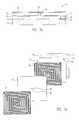
- FIG. 1 adepicts a cross-sectional side view of radio-frequency identification (RFID) transceiver 1 .
- RFIDradio-frequency identification
- FIG. 1 bis an exploded top view of the RFID transceiver of FIG. 1 a.
- FIG. 2is an exploded top view of an alternative RFID transceiver.
- FIG. 3 adepicts a cross-sectional side view of a further alternative RFID transceiver having multiple antenna layers that are directly, electronically connected to each other.
- FIG. 3 bis an exploded top view of the RFID transceiver of FIG. 3 a.
- FIG. 4 adepicts a cross-sectional side view of an alternative RFID transceiver having multiple antenna layers that are not directly, electronically connected to each other.
- FIG. 4 bis an exploded top view of the RFID transceiver of FIG. 4 a.
- FIG. 5is a flow chart of an exemplary method 50 of making an RFID transceiver.
- FIG. 6is a flow chart of an exemplary method 60 of making an alternative RFID transceiver.
- FIG. 1 adepicts a cross-sectional side view of radio-frequency identification (RFID) transceiver 1 in accordance with one embodiment of the present invention.
- RFID transceiver 1includes integrated circuit 10 .
- Integrated circuit 10includes an RFID transceiver circuit and at least one contact area 12 , and may include accompanying control or processing circuitry.
- Insulating layer 20is superimposed over the top surface of integrated circuit 10
- antenna layer 30is superimposed over the top surface of insulating layer 20 .
- Insulating layer 20provides electrical insulation between integrated circuit 10 and antenna layer 30 .
- Electrical conductor 34electrically connects contact area 12 of integrated circuit 10 to antenna layer 30 , through insulating layer 20 .
- Contact area 12may be, for example, a metal input/output pad, a semiconductor area, or any other desired part of integrated circuit 10 .
- Contact area 12provides either direct electrical connection to the RFID transceiver circuit or indirect electrical connection to the RFID transceiver circuit through an intervening connection to accompanying processing or control circuitry.
- the term “electrically connects” and variations thereofare used broadly herein to mean providing an electrically conductive path between the “electrically connected” structures, which may be due to a direct or indirect physical connection.
- FIG. 1 bis an exploded top view of RFID transceiver 1 , wherein integrated circuit 10 , insulating layer 20 , and antenna layer 30 are separated for illustration.
- Insulating layer 20contains at least one contact via 24 through which electrical conductor 34 extends so as to electrically connect integrated circuit 10 to antenna layer 30 .
- Antenna layer 30follows a pattern that conforms to a desired antenna design.
- FIG. 1 bis an exemplary embodiment in which antenna layer 30 has a spiral pattern.
- Antenna layer 30acts as a radio-frequency antenna and receives an electrical stimulus signal that has been radio-transmitted to RFID transceiver 1 from external polling equipment.
- an electrical stimulus signalis a radio-frequency tone (electronic sinewave-shaped signals having specific frequencies) or a simple modulation thereof.
- Antenna layer 30passes the electrical stimulus signal to integrated circuit 10 .
- Integrated circuit 10generates a desired electrical response signal, and passes the electrical response signal back to antenna layer 30 .
- Antenna layer 30then radio-transmits the generated electrical response signal.
- an electrical response signalis a radio-frequency tone or a simple modulations thereof.
- a specific response signalindicates a particular RFID transceiver and thereby implicitly identifies the individual item, such as a piece of clothing or an individual animal, into which the particular RFID transceiver is installed. More complex stimulus and response signals may be used for more demanding applications, such as identification of individuals or equipment for military uses.
- FIG. 2is an exploded top view of an alternative embodiment of an RFID transceiver 2 within the present invention.
- Integrated circuit 10 , insulating layer 20 , and antenna layer 30 of RFID transceiver 2are similar to those of RFID transceiver 1 of FIGS. 1 a , 1 b , except that RFID transceiver 2 of FIG. 2 has two contact vias 24 extending through insulating layer 20 .
- An electrical conductor 34extends through each of the contact vias 24 and respectively provides electrical connection between integrated circuit 10 and antenna layer 30 .
- the pattern of antenna layer 30is serpentine, and the respective ends of antenna layer 30 are electrically connected to a different contact area 12 of integrated circuit 10 .
- antenna layer 30 and integrated circuit 10can be electrically connected at a single point, as in RFID transceiver 1 of FIGS. 1 a , 1 b , or at multiple points, as in RFID transceiver 2 of FIG. 2 .
- the design of antenna layer 30may, among other possibilities, form either: (1) a single, physically continuous antenna, (2) multiple, separate antenna elements that work in concert, (3) multiple separate antennas that work independently, or (4) a part of a larger, multiple-layer antenna.
- the electrical operation of antenna layer 30will depend on the layer design, the location of electrical connection with integrated circuit 10 and the operation of integrated circuit 10 .
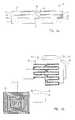
- FIG. 3 adepicts a cross-sectional side view of another alternative embodiment of an RFID transceiver 3 within the present invention.
- RFID transceiver 3includes an integrated circuit 10 , first insulating layer 20 , and first antenna layer 30 similar to those of RFID transceiver 1 of FIG. 1 a .
- RFID transceiver 3also includes a second insulating layer 22 over first antenna layer 30 , and a second antenna layer 32 over second insulating layer 22 .
- Antenna layers 30 and 32are electrically connected, thereby forming a two-layer antenna that is approximately twice as long as the single-layer antennas of RFID transceivers 1 and 2 of FIGS. 1 a , 1 b and 2 .
- FIG. 3 bprovides an exploded top view of RFID transceiver 3 of FIG. 3 a with the layers separated for illustration.
- a first contact via 24extends through first insulating layer 20 .
- a first electrical conductor 34extends through contact via 24 and provides electrical connection between integrated circuit 10 and first antenna layer 30 .
- a second contact via 26extends through second insulating layer 22 .
- Second electrical conductor 36extends through second contact via 26 and provides electrical connection between second antenna layer 32 and first antenna layer 30 .
- Second electrical conductor 36increases the length of the antenna of RFID transceiver 3 by adding the length of second antenna layer 32 to that of first antenna layer 30 .
- the present inventionallows the use of multiple antenna layers, such as are found in FIGS. 3 a , 3 b , to produce a final antenna of a desired length and design that will have a desired electrical resonance or operation at a desired radio-frequency.
- FIG. 4 adepicts a cross-sectional side view of a further alternative embodiment of an RFID transceiver 4 in accordance with the present invention.
- RFID transceiver 4 of FIG. 4 aincludes an integrated circuit 10 , first and second insulating layers 20 and 22 , and first and second antenna layers 30 and 32 , similar to those seen in FIGS. 3 a , 3 b.
- FIG. 4 bis an exploded top view of RFID transceiver 4 .
- a first contact via 24 and a first electrical conductor 34extend through first insulating layer 20 and provide electrical connection between first antenna layer 30 and first contact area 12 of integrated circuit 10 .
- a second contact via 26 and a second electrical conductor 36extend through second insulating layer 22 , first antenna layer 30 , and first insulating layer 20 .
- Second electrical conductor 36provides electrical connection between second antenna layer 32 and a second contact area 12 of integrated circuit 10 , without a direct electrical connection to first antenna layer 30 .
- antenna layers 30 and 32may be used, for example, as separate antenna structures, as seen in FIG. 4 b .
- Exemplary uses for the separate antennas of RFID transceiver 4are to respond to two different stimulus signals or to transmit two different electrical response signals.
- antenna layer 30may be designed as a shielding layer held at a reference voltage (e.g., ground voltage) that electrically isolates second antenna layer 32 from the circuitry below.
- FIG. 5is a flow chart of an exemplary method 50 of making an RFID transceiver in accordance with the present invention. For the sake of example, assume that method 50 is used to make RFID transceiver 1 of FIGS. 1 a , 1 b . The order of the steps may vary.
- an integrated circuit 10that includes an RFID transceiver circuit.
- the active, top surface of integrated circuit 10includes an exposed, contact area 12 with a top surface that serves as an input/output connector for creating electrical contact with integrated circuit 10 .
- a first insulating layer 20is applied onto the top surface of integrated circuit 10 .
- First insulating layer 20may be formed of any insulating material that is compatible with a semiconductor chip, such as spin-on glass, polyimide, SiO 2 , or silicon nitride. This material may be spun-on, deposited, or grown using any convenient method, such as those commonly used in semiconductor chip manufacture or packaging.
- insulating layer 20will be applied over the entire top surface of integrated circuit 10 , including over contact area 12 .
- insulating layer 20may be applied around and not covering contact area 12 , obviating the need for step 53 which is discussed below.
- a first contact via 24is formed through first insulating layer 20 so as to expose contact area 12 of integrated circuit 10 .
- First contact via 24can be formed using any convenient method, such as photo-lithography including etching, e-beam lithography including etching, or contact molding.
- first contact via 24is filled with an electrically conductive material so as to form electrical conductor 34 .
- Conductor 34makes electrical connection to the exposed surface of contact area 12 .
- the material used to fill first contact via 24can be any electrically conductive material, such as metal, doped semiconductor, doped polymer, metal-filled epoxy, or electrically conductive ink.
- the material of electrical conductor 34may be applied by a variety of convenient methods, such as chemical vapor deposition, sputtering, plating, screening, and spin-on, among other possibilities.
- an electrically conductive layeris formed onto the top surface of first insulating layer 20 .
- the electrically conductive layermay be made of any electrically conductive material, such as metal, doped semiconductor, doped polymer, metal-filled epoxy, or electrically conductive ink.
- the material of the electrically conductive layermay be applied by a variety of convenient methods, such as chemical vapor deposition, sputtering, plating, screening, and spin-on, among other possibilities.
- the electrically conductive layeris also applied onto the exposed top surface of electrical conductor 34 , thereby forming an electrical connection between contact area 12 and the electrically conductive layer through electrical conductor 34 .
- Steps 55 and 57may be done simultaneously by having the material of the conductive layer also fill first contact via 24 .
- the electrically conductive layeris patterned to form a first antenna layer 30 .
- Patterningmay be done using any convenient method, such as photo-lithography including etching, e-beam lithography including etching, or contact molding.
- a patterned antenna layer 30may be applied directly onto the first insulating layer 20 through contact printing, screening, or any other method for transferring a pattern of material onto a surface.
- a pre-patterned conductive antenna layer 30for example, a patterned metal foil, may be attached onto the top surface of insulating layer 20 and over electrical conductor 34 .
- FIG. 6is a flow chart of an exemplary method 60 of making an alternative RFID transceiver in accordance with the present invention.
- method 60is used to make RFID transceiver 3 of FIGS. 3 a , 3 b .
- Steps 51 through 59are followed as in method 50 .
- steps 52 through 59 of method 50are repeated, as steps 62 through 69 , to form a second insulating layer 22 and a second antenna layer 32 onto the top surface of first antenna layer 30 .
- a second contact via 26 and a second electrical conductor 36are formed through second insulating layer 22 so as to electrically connect second antenna layer 32 to first antenna layer 30 .
- the location of second electrical conductor 36can be chosen so that it is not directly over first electrical conductor 34 . Staggering the locations of electrical conductors 34 and 36 can improve the planarity of the RFID transceiver.
- method 60may be used to make RFID transceiver 4 of FIGS. 4 a , 4 b .
- second contact via 26 and second electrical conductor 36are formed in steps 63 and 65 respectively to extend through second insulating layer 22 , first antenna layer 30 , and first insulating layer 20 .
- Second electrical conductor 36electrically connects second antenna layer 32 and a second contact area 12 of integrated circuit 10 , without directly electrically connecting to first antenna layer 30 . This allows antenna layers 30 and 32 to be used, for example, as separate antenna structures, as seen in FIG. 4 b.
Landscapes
- Engineering & Computer Science (AREA)
- Physics & Mathematics (AREA)
- Computer Hardware Design (AREA)
- Microelectronics & Electronic Packaging (AREA)
- General Physics & Mathematics (AREA)
- Theoretical Computer Science (AREA)
- Computer Networks & Wireless Communication (AREA)
- Electromagnetism (AREA)
- Power Engineering (AREA)
- Computer Security & Cryptography (AREA)
- General Engineering & Computer Science (AREA)
- Details Of Aerials (AREA)
Abstract
Description
Claims (21)
Priority Applications (1)
| Application Number | Priority Date | Filing Date | Title |
|---|---|---|---|
| US09/631,449US6424315B1 (en) | 2000-08-02 | 2000-08-02 | Semiconductor chip having a radio-frequency identification transceiver |
Applications Claiming Priority (1)
| Application Number | Priority Date | Filing Date | Title |
|---|---|---|---|
| US09/631,449US6424315B1 (en) | 2000-08-02 | 2000-08-02 | Semiconductor chip having a radio-frequency identification transceiver |
Publications (1)
| Publication Number | Publication Date |
|---|---|
| US6424315B1true US6424315B1 (en) | 2002-07-23 |
Family
ID=24531252
Family Applications (1)
| Application Number | Title | Priority Date | Filing Date |
|---|---|---|---|
| US09/631,449Expired - LifetimeUS6424315B1 (en) | 2000-08-02 | 2000-08-02 | Semiconductor chip having a radio-frequency identification transceiver |
Country Status (1)
| Country | Link |
|---|---|
| US (1) | US6424315B1 (en) |
Cited By (105)
| Publication number | Priority date | Publication date | Assignee | Title |
|---|---|---|---|---|
| US20020171602A1 (en)* | 2001-05-18 | 2002-11-21 | Atmel Germany Gmbh | Method for tuning an antenna resonant circuit of a passive transponder |
| US20030080918A1 (en)* | 2001-10-29 | 2003-05-01 | Forster Ian James | Wave antenna wireless communication device and method |
| US20030132893A1 (en)* | 2001-10-29 | 2003-07-17 | Forster Ian J. | Wave antenna wireless communication device and method |
| US20030137421A1 (en)* | 2002-01-17 | 2003-07-24 | Peter Herkenrath | Protective working device for miners |
| US20030156032A1 (en)* | 2001-07-12 | 2003-08-21 | Adams Matthew Thomas | Method and apparatus for configuring the read-range of an RFID label or tag |
| US6636180B2 (en)* | 2001-08-10 | 2003-10-21 | Hon Hai Precision Ind. Co., Ltd. | Printed circuit board antenna |
| US6646328B2 (en)* | 2002-01-11 | 2003-11-11 | Taiwan Semiconductor Manufacturing Co. Ltd. | Chip antenna with a shielding layer |
| US6660559B1 (en) | 2001-06-25 | 2003-12-09 | Amkor Technology, Inc. | Method of making a chip carrier package using laser ablation |
| US20030235027A1 (en)* | 2002-01-09 | 2003-12-25 | Larry Smeyak | Method of making interactive information closure and package |
| US20040027241A1 (en)* | 2002-08-08 | 2004-02-12 | Forster Ian J. | Vehicle tag reader |
| US20040032377A1 (en)* | 2001-10-29 | 2004-02-19 | Forster Ian James | Wave antenna wireless communication device and method |
| US20040036572A1 (en)* | 2002-04-24 | 2004-02-26 | Forster Ian J. | Wireless communication device having conductive elements antenna |
| US20040053447A1 (en)* | 2001-06-29 | 2004-03-18 | Foster Donald Craig | Leadframe having fine pitch bond fingers formed using laser cutting method |
| WO2004042868A1 (en)* | 2002-11-07 | 2004-05-21 | Fractus, S.A. | Integrated circuit package including miniature antenna |
| WO2004032343A3 (en)* | 2002-10-02 | 2004-07-01 | Univ Florida | Single chip radio with integrated antenna |
| US20040159932A1 (en)* | 2003-02-18 | 2004-08-19 | Hiroto Watanabe | Semiconductor device |
| US20040189530A1 (en)* | 2003-03-28 | 2004-09-30 | Gemtek Technology Co., Ltd. | Dual frequency band inverted-F antenna |
| US20050023476A1 (en)* | 2003-07-31 | 2005-02-03 | Eastman Kodak Company | Digital film grain |
| US20050093761A1 (en)* | 2002-08-14 | 2005-05-05 | King Patrick F. | RFID tire belt antenna system and method |
| US20050140512A1 (en)* | 2003-12-25 | 2005-06-30 | Isao Sakama | Wireless IC tag, and method and apparatus for manufacturing the same |
| US20050138798A1 (en)* | 2003-12-25 | 2005-06-30 | Isao Sakama | Radio IC tag, method for manufacturing radio IC tag, and apparatus for manufacturing radio IC tag |
| US20050167797A1 (en)* | 2004-01-29 | 2005-08-04 | Advanpack Solutions Pte Ltd | Structure package |
| US20050206576A1 (en)* | 2004-03-16 | 2005-09-22 | Stmicroelectronics S.A. | Semiconductor device with antenna and collector screen |
| US20050280504A1 (en)* | 2004-06-22 | 2005-12-22 | Vubiq Incorporated, A Nevada Corporation | RFID system utilizing parametric reflective technology |
| WO2005074402A3 (en)* | 2004-02-10 | 2006-01-12 | Cyrips Pte Ltd | An integrated circuit |
| US7015868B2 (en) | 1999-09-20 | 2006-03-21 | Fractus, S.A. | Multilevel Antennae |
| US7044426B1 (en)* | 2002-07-30 | 2006-05-16 | Allmon James A | Fitting for building structures and the like |
| US20060146739A1 (en)* | 2004-12-03 | 2006-07-06 | Pentax Corporation | Operation control method of two dimensional diffusive signal-transmission devices, signal communication apparatus, and clothing provided with antenna function |
| US7106173B2 (en) | 2003-01-03 | 2006-09-12 | Battelle Memorial Institute | Tags, wireless communication systems, tag communication methods, and wireless communications methods |
| US20060231624A1 (en)* | 2005-04-18 | 2006-10-19 | Tomoki Kobayashi | Reader/writer and manufacturing method thereof |
| US20060276157A1 (en)* | 2005-06-03 | 2006-12-07 | Chen Zhi N | Apparatus and methods for packaging antennas with integrated circuit chips for millimeter wave applications |
| US20070029481A1 (en)* | 2003-08-01 | 2007-02-08 | Robert Morrison | Specimen tip and tip holder assembly |
| US20070060311A1 (en)* | 2005-09-12 | 2007-03-15 | Igt | Enhanced gaming chips and table game security |
| US20070115130A1 (en)* | 2005-11-14 | 2007-05-24 | Ronald Eveland | Multi-dimensional, broadband track and trace sensor radio frequency identification device |
| US20070139206A1 (en)* | 2004-12-16 | 2007-06-21 | Fujitsu Limited | RFID tag |
| US20070171129A1 (en)* | 2006-01-24 | 2007-07-26 | Avery Dennison Corporation | Radio frequency (RF) antenna containing element and methods of making the same |
| US20070222684A1 (en)* | 2006-03-21 | 2007-09-27 | Cypress Semiconductor Corp. | Multiple layer antenna for wireless applications |
| US20070229264A1 (en)* | 2005-11-14 | 2007-10-04 | Ronald Eveland | Software method and system for encapsulation of RFID data into a standardized globally routable format |
| WO2007111417A1 (en)* | 2006-03-24 | 2007-10-04 | Byung-Deuk Choi | Transponder for radio frequency identification system |
| US20070262866A1 (en)* | 2005-11-14 | 2007-11-15 | Ronald Eveland | Multi-Dimensional Broadband Track and Trace Sensor Radio Frequency Identification Device |
| US20070285239A1 (en)* | 2006-06-12 | 2007-12-13 | Easton Martyn N | Centralized optical-fiber-based RFID systems and methods |
| US20080012709A1 (en)* | 2006-07-14 | 2008-01-17 | Eyes Open Corporation | Information carrier arrangement, washable textile goods and electronic ear tag for living beings |
| US20080023810A1 (en)* | 2006-07-28 | 2008-01-31 | Semiconductor Energy Laboratory Co., Ltd. | Semiconductor device |
| US20080023793A1 (en)* | 2006-07-28 | 2008-01-31 | Semiconductor Energy Laboratory Co., Ltd. | Semiconductor device |
| US20080029897A1 (en)* | 2006-08-07 | 2008-02-07 | Rcd Technology Inc. | Side connectors for rfid chip |
| US20080062049A1 (en)* | 2004-09-27 | 2008-03-13 | Fractus, S.A. | Tunable Antenna |
| US7348887B1 (en) | 2004-06-15 | 2008-03-25 | Eigent Technologies, Llc | RFIDs embedded into semiconductors |
| US20080100440A1 (en)* | 2006-10-31 | 2008-05-01 | Downie John D | Radio frequency identification transponder for communicating condition of a component |
| US20080143486A1 (en)* | 2006-12-14 | 2008-06-19 | Downie John D | Signal-processing systems and methods for RFID-tag signals |
| US20080218355A1 (en)* | 2007-03-09 | 2008-09-11 | Downie John D | Optically addressed RFID elements |
| US20080257407A1 (en)* | 2004-11-17 | 2008-10-23 | Nanosys, Inc. | Photoactive Devices and Components with Enhanced Efficiency |
| US20080265038A1 (en)* | 2004-07-23 | 2008-10-30 | Fractus, S.A. | Antenna in Package with Reduced Electromagnetic Interaction with on Chip Elements |
| US20080284659A1 (en)* | 2007-05-18 | 2008-11-20 | Kabushiki Kaisha Tokai Rika Denki Seisakusho | Antenna structure for wireless communication device |
| US20090009403A1 (en)* | 2007-07-06 | 2009-01-08 | Laird Technologies, Inc. | Antenna assembly with connectors having an internal conductive channel |
| US20090045961A1 (en)* | 2007-08-13 | 2009-02-19 | Aravind Chamarti | Antenna systems for passive RFID tags |
| US20090267859A1 (en)* | 2008-04-29 | 2009-10-29 | Ls Mtron, Ltd. | End-fed planar type spiral antenna |
| US20090283602A1 (en)* | 2006-07-10 | 2009-11-19 | Nxp B.V. | Integrated Circuit Transponder, Method of Producing an Integrated Circuit and Method of Producing a Transponder |
| US20100016681A1 (en)* | 2008-07-15 | 2010-01-21 | Charles Jr Harry K | Apparatus and Methods for Monitoring Physiological Functions |
| US20100026601A1 (en)* | 2008-08-04 | 2010-02-04 | Chung-Long Chang | Antennas Integrated in Semiconductor Chips |
| US7712674B1 (en) | 2005-02-22 | 2010-05-11 | Eigent Technologies Llc | RFID devices for verification of correctness, reliability, functionality and security |
| US20100141547A1 (en)* | 2004-06-16 | 2010-06-10 | Axalto Sa | Shielded contactless electronic document |
| US7760094B1 (en) | 2006-12-14 | 2010-07-20 | Corning Cable Systems Llc | RFID systems and methods for optical fiber network deployment and maintenance |
| US7772981B1 (en) | 2006-05-08 | 2010-08-10 | Rexam Closures And Containers Inc. | Non-removable closure with integral RFID |
| US7772975B2 (en) | 2006-10-31 | 2010-08-10 | Corning Cable Systems, Llc | System for mapping connections using RFID function |
| US7782202B2 (en) | 2006-10-31 | 2010-08-24 | Corning Cable Systems, Llc | Radio frequency identification of component connections |
| US20100245057A1 (en)* | 2009-03-31 | 2010-09-30 | Aravind Chamarti | Components, systems, and methods for associating sensor data with component location |
| US20110057628A1 (en)* | 2006-07-28 | 2011-03-10 | Semiconductor Energy Laboratory Co., Ltd. | Power storage device |
| US20110074650A1 (en)* | 2009-09-30 | 2011-03-31 | Shenzhen Futaihong Precision Industry Co., Ltd. | Antenna module and housing having the same |
| US20110140856A1 (en)* | 2009-11-30 | 2011-06-16 | John David Downie | RFID Condition Latching |
| US7965186B2 (en) | 2007-03-09 | 2011-06-21 | Corning Cable Systems, Llc | Passive RFID elements having visual indicators |
| US7973664B1 (en) | 2006-08-04 | 2011-07-05 | Rexam Healthcare Packaging Inc. | Closure having RFID and foil |
| US20110174885A1 (en)* | 2008-07-15 | 2011-07-21 | Syntag Manufacturing, LLC | Durable rfid tag |
| US20110181484A1 (en)* | 2007-06-22 | 2011-07-28 | Vubiq, Inc. | Integrated antenna and chip package and method of manufacturing thereof |
| US20110315774A1 (en)* | 2010-06-25 | 2011-12-29 | Fujitsu Frontech Limited | Wireless tag and manufacturing method |
| US8172468B2 (en) | 2010-05-06 | 2012-05-08 | Corning Incorporated | Radio frequency identification (RFID) in communication connections, including fiber optic components |
| US20120112980A1 (en)* | 2010-11-03 | 2012-05-10 | Andrei Kaikkonen | Antenna Arrangement and a Portable Radio Communication Device Comprising Such An Antenna Arrangement |
| US8196829B2 (en) | 2006-06-23 | 2012-06-12 | Fractus, S.A. | Chip module, sim card, wireless device and wireless communication method |
| US8248208B2 (en) | 2008-07-15 | 2012-08-21 | Corning Cable Systems, Llc. | RFID-based active labeling system for telecommunication systems |
| US8264355B2 (en) | 2006-12-14 | 2012-09-11 | Corning Cable Systems Llc | RFID systems and methods for optical fiber network deployment and maintenance |
| US8385461B1 (en) | 2009-04-20 | 2013-02-26 | Vubiq, Inc. | On-off keying using vector modulation |
| US20130318778A1 (en)* | 2012-06-01 | 2013-12-05 | Tzuh-Suan Wang | Method for manufacturing antenna structure |
| US8731405B2 (en) | 2008-08-28 | 2014-05-20 | Corning Cable Systems Llc | RFID-based systems and methods for collecting telecommunications network information |
| US8796740B1 (en)* | 2009-01-13 | 2014-08-05 | Altera Corporation | Using a single mask for various design configurations |
| US20140340264A1 (en)* | 2013-05-17 | 2014-11-20 | Lorom Industrial Co., Ltd. | Antenna structure |
| US8931166B2 (en) | 2011-05-19 | 2015-01-13 | Tecnomar Oy | Manufacturing method of electrical bridges suitable for reel to reel mass manufacturing |
| US9088058B2 (en) | 2009-08-19 | 2015-07-21 | Vubiq Networks, Inc. | Waveguide interface with a launch transducer and a circular interface plate |
| RU2565524C1 (en)* | 2014-04-25 | 2015-10-20 | Федеральное государственное унитарное предприятие "Центральный научно-исследовательский радиотехнический институт имени академика А.И. Берга" | Flat helical antenna |
| US9165232B2 (en) | 2012-05-14 | 2015-10-20 | Corning Incorporated | Radio-frequency identification (RFID) tag-to-tag autoconnect discovery, and related methods, circuits, and systems |
| US9231290B2 (en) | 2010-06-14 | 2016-01-05 | Avery Dennison Corporation | Method for making short run radio frequency identification tags and labels |
| US9472859B2 (en) | 2014-05-20 | 2016-10-18 | International Business Machines Corporation | Integration of area efficient antennas for phased array or wafer scale array antenna applications |
| US20160372979A1 (en)* | 2014-03-14 | 2016-12-22 | Murata Manufacturing Co., Ltd. | Wireless power supplying apparatus |
| US9563832B2 (en) | 2012-10-08 | 2017-02-07 | Corning Incorporated | Excess radio-frequency (RF) power storage and power sharing RF identification (RFID) tags, and related connection systems and methods |
| US9652708B2 (en) | 2006-10-31 | 2017-05-16 | Fiber Mountain, Inc. | Protocol for communications between a radio frequency identification (RFID) tag and a connected device, and related systems and methods |
| US9652709B2 (en) | 2006-10-31 | 2017-05-16 | Fiber Mountain, Inc. | Communications between multiple radio frequency identification (RFID) connected tags and one or more devices, and related systems and methods |
| US9652707B2 (en) | 2006-10-31 | 2017-05-16 | Fiber Mountain, Inc. | Radio frequency identification (RFID) connected tag communications protocol and related systems and methods |
| US9705202B2 (en) | 2009-01-07 | 2017-07-11 | Sony Corporation | Semiconductor device, method of manufacturing the same, in-millimeter-wave dielectric transmission device, method of manufacturing the same, and in-millimeter-wave dielectric transmission system |
| US9899737B2 (en) | 2011-12-23 | 2018-02-20 | Sofant Technologies Ltd | Antenna element and antenna device comprising such elements |
| US10032102B2 (en) | 2006-10-31 | 2018-07-24 | Fiber Mountain, Inc. | Excess radio-frequency (RF) power storage in RF identification (RFID) tags, and related systems and methods |
| US10320047B2 (en) | 2009-08-19 | 2019-06-11 | Vubiq Networks, Inc. | Waveguide assembly comprising a molded waveguide interface having a support block for a launch transducer that is coupled to a communication device through a flange attached to the interface |
| US10366321B2 (en)* | 2015-02-27 | 2019-07-30 | Murata Manufacturing Co., Ltd. | RFIC device and method for manufacturing resin molded body including RFIC device |
| US10453055B2 (en) | 2012-02-12 | 2019-10-22 | Cytherean Mandelbrot LLC | Method for secure electronic tender |
| US10818997B2 (en) | 2017-12-29 | 2020-10-27 | Vubiq Networks, Inc. | Waveguide interface and printed circuit board launch transducer assembly and methods of use thereof |
| US11216625B2 (en) | 2018-12-05 | 2022-01-04 | Vubiq Networks, Inc. | High bit density millimeter wave RFID systems, devices, and methods of use thereof |
| US20220172019A1 (en)* | 2019-04-10 | 2022-06-02 | Sk-Electronics Co., Ltd. | Contactless information carrier |
| US20220198241A1 (en)* | 2020-12-22 | 2022-06-23 | Fujifilm Corporation | Noncontact communication medium |
Citations (4)
| Publication number | Priority date | Publication date | Assignee | Title |
|---|---|---|---|---|
| US5808587A (en)* | 1994-03-24 | 1998-09-15 | Hochiki Corporation | Wireless access control system using a proximity member and antenna equipment therefor |
| WO2000013438A1 (en) | 1998-08-28 | 2000-03-09 | Woodtoga Holdings Company | A wireless signal containing data from a memory |
| US6118379A (en)* | 1997-12-31 | 2000-09-12 | Intermec Ip Corp. | Radio frequency identification transponder having a spiral antenna |
| US6147662A (en)* | 1999-09-10 | 2000-11-14 | Moore North America, Inc. | Radio frequency identification tags and labels |
- 2000
- 2000-08-02USUS09/631,449patent/US6424315B1/ennot_activeExpired - Lifetime
Patent Citations (4)
| Publication number | Priority date | Publication date | Assignee | Title |
|---|---|---|---|---|
| US5808587A (en)* | 1994-03-24 | 1998-09-15 | Hochiki Corporation | Wireless access control system using a proximity member and antenna equipment therefor |
| US6118379A (en)* | 1997-12-31 | 2000-09-12 | Intermec Ip Corp. | Radio frequency identification transponder having a spiral antenna |
| WO2000013438A1 (en) | 1998-08-28 | 2000-03-09 | Woodtoga Holdings Company | A wireless signal containing data from a memory |
| US6147662A (en)* | 1999-09-10 | 2000-11-14 | Moore North America, Inc. | Radio frequency identification tags and labels |
Non-Patent Citations (3)
| Title |
|---|
| Alexopoulos, N., "Substrate Optimization for Integrated Circuit Antennas," IEEE Transactions on Microwave Theory and Techniques, vol. MTT-31, No. 7, Jul. 1983, pp. 550-557. |
| Flynt et al., "Low Cost and Compact Active Integrated Antenna Transceiver for System Applications," IEEE Transactions on microwave Theory and Techniques, vol. 44, No. 10, Oct. 1996, pp. 1642-1649. |
| Rebeiz, G., "Millimeter-Wave and Terahertz Integrated Circuit Antennas", Proceedings of the IEEE, vol. 80, No. 11, Nov. 1992, pp. 1748-1770. |
Cited By (249)
| Publication number | Priority date | Publication date | Assignee | Title |
|---|---|---|---|---|
| US7123208B2 (en) | 1999-09-20 | 2006-10-17 | Fractus, S.A. | Multilevel antennae |
| US10056682B2 (en) | 1999-09-20 | 2018-08-21 | Fractus, S.A. | Multilevel antennae |
| US8941541B2 (en) | 1999-09-20 | 2015-01-27 | Fractus, S.A. | Multilevel antennae |
| US8976069B2 (en) | 1999-09-20 | 2015-03-10 | Fractus, S.A. | Multilevel antennae |
| US9000985B2 (en) | 1999-09-20 | 2015-04-07 | Fractus, S.A. | Multilevel antennae |
| US9054421B2 (en) | 1999-09-20 | 2015-06-09 | Fractus, S.A. | Multilevel antennae |
| US7397431B2 (en) | 1999-09-20 | 2008-07-08 | Fractus, S.A. | Multilevel antennae |
| US9240632B2 (en) | 1999-09-20 | 2016-01-19 | Fractus, S.A. | Multilevel antennae |
| US7015868B2 (en) | 1999-09-20 | 2006-03-21 | Fractus, S.A. | Multilevel Antennae |
| US8154462B2 (en) | 1999-09-20 | 2012-04-10 | Fractus, S.A. | Multilevel antennae |
| US7394432B2 (en) | 1999-09-20 | 2008-07-01 | Fractus, S.A. | Multilevel antenna |
| US9362617B2 (en) | 1999-09-20 | 2016-06-07 | Fractus, S.A. | Multilevel antennae |
| US8009111B2 (en) | 1999-09-20 | 2011-08-30 | Fractus, S.A. | Multilevel antennae |
| US9761934B2 (en) | 1999-09-20 | 2017-09-12 | Fractus, S.A. | Multilevel antennae |
| US8154463B2 (en) | 1999-09-20 | 2012-04-10 | Fractus, S.A. | Multilevel antennae |
| US8330659B2 (en) | 1999-09-20 | 2012-12-11 | Fractus, S.A. | Multilevel antennae |
| US7505007B2 (en) | 1999-09-20 | 2009-03-17 | Fractus, S.A. | Multi-level antennae |
| US7528782B2 (en) | 1999-09-20 | 2009-05-05 | Fractus, S.A. | Multilevel antennae |
| US6952560B2 (en)* | 2001-05-18 | 2005-10-04 | Atmel Germany Gbmh | Tuned antenna resonant circuit of a passive transponder |
| US20020171602A1 (en)* | 2001-05-18 | 2002-11-21 | Atmel Germany Gmbh | Method for tuning an antenna resonant circuit of a passive transponder |
| US6660559B1 (en) | 2001-06-25 | 2003-12-09 | Amkor Technology, Inc. | Method of making a chip carrier package using laser ablation |
| US20040053447A1 (en)* | 2001-06-29 | 2004-03-18 | Foster Donald Craig | Leadframe having fine pitch bond fingers formed using laser cutting method |
| US7106196B2 (en)* | 2001-07-12 | 2006-09-12 | Intermec Ip Corp | Method and apparatus for configuring the read-range of an RFID label or tag |
| US20030156032A1 (en)* | 2001-07-12 | 2003-08-21 | Adams Matthew Thomas | Method and apparatus for configuring the read-range of an RFID label or tag |
| US6636180B2 (en)* | 2001-08-10 | 2003-10-21 | Hon Hai Precision Ind. Co., Ltd. | Printed circuit board antenna |
| US7373713B2 (en) | 2001-10-29 | 2008-05-20 | Mineral Lassen Llc | Wave antenna wireless communication device and method |
| US7190319B2 (en) | 2001-10-29 | 2007-03-13 | Forster Ian J | Wave antenna wireless communication device and method |
| US20030080918A1 (en)* | 2001-10-29 | 2003-05-01 | Forster Ian James | Wave antenna wireless communication device and method |
| US20030080919A1 (en)* | 2001-10-29 | 2003-05-01 | Forster Ian James | Wave antenna wireless communication device and method |
| US7746285B2 (en) | 2001-10-29 | 2010-06-29 | Ian James Forster | Wave antenna wireless communication device and method |
| US20100231360A1 (en)* | 2001-10-29 | 2010-09-16 | Ian James Forster | Wave antenna wireless communication device and method |
| US20050193549A1 (en)* | 2001-10-29 | 2005-09-08 | Forster Ian J. | Wave antenna wireless communication device and method |
| US20030117334A1 (en)* | 2001-10-29 | 2003-06-26 | Forster Ian James | Wave antenna wireless communication device and method |
| US20030132893A1 (en)* | 2001-10-29 | 2003-07-17 | Forster Ian J. | Wave antenna wireless communication device and method |
| US7439928B2 (en) | 2001-10-29 | 2008-10-21 | Mineral Lassen Llc | Wave antenna wireless communication device and method |
| US6630910B2 (en)* | 2001-10-29 | 2003-10-07 | Marconi Communications Inc. | Wave antenna wireless communication device and method |
| US20080235937A1 (en)* | 2001-10-29 | 2008-10-02 | Mineral Lassen Llc | Wave antenna wireless communication device and method |
| US7916095B2 (en) | 2001-10-29 | 2011-03-29 | Mineral Lassen Llc | Wave antenna wireless communication device and method |
| US7420520B2 (en) | 2001-10-29 | 2008-09-02 | Mineral Lassen Llc | Wave antenna wireless communication device and method |
| US6895655B2 (en) | 2001-10-29 | 2005-05-24 | Marconi Intellectual Property (Us) Inc. | Wave antenna wireless communication device and method |
| US20060050001A1 (en)* | 2001-10-29 | 2006-03-09 | Mineral Lassen Llc | Wave antenna wireless communication device and method |
| US20070057861A1 (en)* | 2001-10-29 | 2007-03-15 | Forster Ian J | Wave antenna wireless communication device and method |
| US6853347B2 (en) | 2001-10-29 | 2005-02-08 | Marconi Intellectual Property (Us) Inc. | Wave antenna wireless communication device and method |
| US6903704B2 (en) | 2001-10-29 | 2005-06-07 | Mineral Lassen Llc | Wave antenna wireless communication device and method |
| US7345643B2 (en) | 2001-10-29 | 2008-03-18 | Mineral Lassen Llc | Wave antenna wireless communication device and method |
| US20040032377A1 (en)* | 2001-10-29 | 2004-02-19 | Forster Ian James | Wave antenna wireless communication device and method |
| US7375699B2 (en) | 2001-10-29 | 2008-05-20 | Mineral Lassen Llc | Wave antenna wireless communication device and method |
| US20060290588A1 (en)* | 2001-10-29 | 2006-12-28 | Forster Ian J | Wave antenna wireless communication device and method |
| US20060279425A1 (en)* | 2001-10-29 | 2006-12-14 | Mineral Lassen Llc | Wave antenna wireless communication device and method |
| US7093345B2 (en) | 2001-10-29 | 2006-08-22 | Ian James Forster | Wave antenna wireless communication device and method |
| US7394438B2 (en) | 2001-10-29 | 2008-07-01 | Mineral Lassen Llc | Wave antenna wireless communication device and method |
| US20040041739A1 (en)* | 2001-10-29 | 2004-03-04 | Forster Ian James | Wave antenna wireless communication device and method |
| US20030235027A1 (en)* | 2002-01-09 | 2003-12-25 | Larry Smeyak | Method of making interactive information closure and package |
| US6646328B2 (en)* | 2002-01-11 | 2003-11-11 | Taiwan Semiconductor Manufacturing Co. Ltd. | Chip antenna with a shielding layer |
| US20030137421A1 (en)* | 2002-01-17 | 2003-07-24 | Peter Herkenrath | Protective working device for miners |
| US20090256768A1 (en)* | 2002-04-24 | 2009-10-15 | Mineral Lassen Llc | Wireless communication device having conductive elements antenna |
| US7843393B2 (en) | 2002-04-24 | 2010-11-30 | Forster Ian J | Wireless communication device having conductive elements antenna |
| US20040036572A1 (en)* | 2002-04-24 | 2004-02-26 | Forster Ian J. | Wireless communication device having conductive elements antenna |
| US7557767B2 (en) | 2002-04-24 | 2009-07-07 | Forster Ian J | Wireless communication device having conductive elements antenna |
| US20060290579A1 (en)* | 2002-04-24 | 2006-12-28 | Mineral Lassen Llc | Wireless communication device having conductive elements antenna |
| US20110063177A1 (en)* | 2002-04-24 | 2011-03-17 | Forster Ian J | Wireless communication device having conductive elements antenna |
| US7969377B2 (en) | 2002-04-24 | 2011-06-28 | Mineral Lassen Llc | Wireless communication device having conductive elements antenna |
| US20080024384A1 (en)* | 2002-04-24 | 2008-01-31 | Mineral Lassen Llc | Wireless communication device having conductive elements antenna |
| US7327326B2 (en) | 2002-04-24 | 2008-02-05 | Mineral Lassen Llc | Wireless communication device having conductive elements antenna |
| US7239287B2 (en) | 2002-04-24 | 2007-07-03 | Mineral Lassen Llc | Wireless communication device having conductive elements antenna |
| US7044426B1 (en)* | 2002-07-30 | 2006-05-16 | Allmon James A | Fitting for building structures and the like |
| US7586403B2 (en) | 2002-08-08 | 2009-09-08 | Ian J Forster | Vehicle tag reader |
| US7518494B2 (en) | 2002-08-08 | 2009-04-14 | Ian J Forster | Vehicle tag reader |
| US7479873B2 (en) | 2002-08-08 | 2009-01-20 | Mineral Lassen Llc | Vehicle tag reader |
| US20040027241A1 (en)* | 2002-08-08 | 2004-02-12 | Forster Ian J. | Vehicle tag reader |
| US7015802B2 (en) | 2002-08-08 | 2006-03-21 | Forster Ian J | Vehicle tag reader |
| US20070013500A1 (en)* | 2002-08-08 | 2007-01-18 | Mineral Lassen Llc | Vehicle tag reader |
| US20060192662A1 (en)* | 2002-08-08 | 2006-08-31 | Mineral Lassen Llc | Vehicle tag reader |
| US20060170540A1 (en)* | 2002-08-08 | 2006-08-03 | Mineral Lassen Llc | Vehicle tag reader |
| US20050093761A1 (en)* | 2002-08-14 | 2005-05-05 | King Patrick F. | RFID tire belt antenna system and method |
| US7050017B2 (en) | 2002-08-14 | 2006-05-23 | King Patrick F | RFID tire belt antenna system and method |
| US7088964B2 (en) | 2002-10-02 | 2006-08-08 | University Of Florida Research Foundation, Inc. | Single chip radio with integrated antenna |
| US20050113035A1 (en)* | 2002-10-02 | 2005-05-26 | Kenneth Kyongyop O | Single chip radio with integrated antenna |
| WO2004032343A3 (en)* | 2002-10-02 | 2004-07-01 | Univ Florida | Single chip radio with integrated antenna |
| US10056691B2 (en) | 2002-11-07 | 2018-08-21 | Fractus, S.A. | Integrated circuit package including miniature antenna |
| US20100328185A1 (en)* | 2002-11-07 | 2010-12-30 | Jordi Soler Castany | Radio-frequency system in package including antenna |
| US7463199B2 (en) | 2002-11-07 | 2008-12-09 | Fractus, S.A. | Integrated circuit package including miniature antenna |
| US7791539B2 (en) | 2002-11-07 | 2010-09-07 | Fractus, S.A. | Radio-frequency system in package including antenna |
| US8203488B2 (en) | 2002-11-07 | 2012-06-19 | Fractus, S.A. | Integrated circuit package including miniature antenna |
| US9077073B2 (en) | 2002-11-07 | 2015-07-07 | Fractus, S.A. | Integrated circuit package including miniature antenna |
| US20070120742A1 (en)* | 2002-11-07 | 2007-05-31 | Fractus, S.A. | Radio-frequency system in package including antenna |
| US9761948B2 (en) | 2002-11-07 | 2017-09-12 | Fractus, S.A. | Integrated circuit package including miniature antenna |
| WO2004042868A1 (en)* | 2002-11-07 | 2004-05-21 | Fractus, S.A. | Integrated circuit package including miniature antenna |
| US20090085810A1 (en)* | 2002-11-07 | 2009-04-02 | Fractus, S.A. | Integrated circuit package including miniature antenna |
| US10644405B2 (en) | 2002-11-07 | 2020-05-05 | Fractus, S.A. | Integrated circuit package including miniature antenna |
| US10320079B2 (en) | 2002-11-07 | 2019-06-11 | Fractus, S.A. | Integrated circuit package including miniature antenna |
| US20060256018A1 (en)* | 2002-11-07 | 2006-11-16 | Fractus, S.A. | Integrated circuit package including miniature antenna |
| US8421686B2 (en) | 2002-11-07 | 2013-04-16 | Fractus, S.A. | Radio-frequency system in package including antenna |
| US7095372B2 (en) | 2002-11-07 | 2006-08-22 | Fractus, S.A. | Integrated circuit package including miniature antenna |
| US20060033664A1 (en)* | 2002-11-07 | 2006-02-16 | Jordi Soler Castany | Integrated circuit package including miniature antenna |
| US7106173B2 (en) | 2003-01-03 | 2006-09-12 | Battelle Memorial Institute | Tags, wireless communication systems, tag communication methods, and wireless communications methods |
| US20070001810A1 (en)* | 2003-01-03 | 2007-01-04 | Scott Jeff W | Tags, wireless communication systems, tag communication methods, and wireless communications methods |
| US7312528B2 (en)* | 2003-02-18 | 2007-12-25 | Hitachi Maxell, Ltd. | Semiconductor device having antenna connection electrodes |
| US20040159932A1 (en)* | 2003-02-18 | 2004-08-19 | Hiroto Watanabe | Semiconductor device |
| US20040189530A1 (en)* | 2003-03-28 | 2004-09-30 | Gemtek Technology Co., Ltd. | Dual frequency band inverted-F antenna |
| US6930640B2 (en)* | 2003-03-28 | 2005-08-16 | Gemtek Technology Co., Ltd. | Dual frequency band inverted-F antenna |
| US7015479B2 (en) | 2003-07-31 | 2006-03-21 | Eastman Kodak Company | Digital film grain |
| US20050023476A1 (en)* | 2003-07-31 | 2005-02-03 | Eastman Kodak Company | Digital film grain |
| US20070029481A1 (en)* | 2003-08-01 | 2007-02-08 | Robert Morrison | Specimen tip and tip holder assembly |
| US20050140512A1 (en)* | 2003-12-25 | 2005-06-30 | Isao Sakama | Wireless IC tag, and method and apparatus for manufacturing the same |
| US7250867B2 (en)* | 2003-12-25 | 2007-07-31 | Hitachi, Ltd. | Wireless IC tag, and method and apparatus for manufacturing the same |
| US20050138798A1 (en)* | 2003-12-25 | 2005-06-30 | Isao Sakama | Radio IC tag, method for manufacturing radio IC tag, and apparatus for manufacturing radio IC tag |
| US20050167797A1 (en)* | 2004-01-29 | 2005-08-04 | Advanpack Solutions Pte Ltd | Structure package |
| WO2005074402A3 (en)* | 2004-02-10 | 2006-01-12 | Cyrips Pte Ltd | An integrated circuit |
| US20050206576A1 (en)* | 2004-03-16 | 2005-09-22 | Stmicroelectronics S.A. | Semiconductor device with antenna and collector screen |
| FR2867899A1 (en)* | 2004-03-16 | 2005-09-23 | St Microelectronics Sa | SEMICONDUCTOR DEVICE WITH ANTENNA AND COLLECTION SCREEN |
| EP1580837A1 (en)* | 2004-03-16 | 2005-09-28 | STMicroelectronics S.A. | Semiconductor device with antenna and collecting screen |
| US7180450B2 (en) | 2004-03-16 | 2007-02-20 | Stmicroelectronics S.A. | Semiconductor device with antenna and collector screen |
| US7348887B1 (en) | 2004-06-15 | 2008-03-25 | Eigent Technologies, Llc | RFIDs embedded into semiconductors |
| US8487828B2 (en)* | 2004-06-16 | 2013-07-16 | Gemalto, Sa | Shielded contactless electronic document |
| US20100141547A1 (en)* | 2004-06-16 | 2010-06-10 | Axalto Sa | Shielded contactless electronic document |
| US20050280539A1 (en)* | 2004-06-22 | 2005-12-22 | Pettus Michael G | RFID system utilizing parametric reflective technology |
| US7498940B2 (en) | 2004-06-22 | 2009-03-03 | Vubiq, Inc. | RFID system utilizing parametric reradiated technology |
| US7460014B2 (en) | 2004-06-22 | 2008-12-02 | Vubiq Incorporated | RFID system utilizing parametric reflective technology |
| US20050280504A1 (en)* | 2004-06-22 | 2005-12-22 | Vubiq Incorporated, A Nevada Corporation | RFID system utilizing parametric reflective technology |
| US20080265038A1 (en)* | 2004-07-23 | 2008-10-30 | Fractus, S.A. | Antenna in Package with Reduced Electromagnetic Interaction with on Chip Elements |
| US8330259B2 (en) | 2004-07-23 | 2012-12-11 | Fractus, S.A. | Antenna in package with reduced electromagnetic interaction with on chip elements |
| US7924226B2 (en) | 2004-09-27 | 2011-04-12 | Fractus, S.A. | Tunable antenna |
| US20080062049A1 (en)* | 2004-09-27 | 2008-03-13 | Fractus, S.A. | Tunable Antenna |
| US20100001982A1 (en)* | 2004-11-17 | 2010-01-07 | Nanosys, Inc. | Photoactive Devices and Components with Enhanced Efficiency |
| US20080257407A1 (en)* | 2004-11-17 | 2008-10-23 | Nanosys, Inc. | Photoactive Devices and Components with Enhanced Efficiency |
| US20080257406A1 (en)* | 2004-11-17 | 2008-10-23 | Nanosys, Inc. | Photoactive Devices and Components with Enhanced Efficiency |
| US20060146739A1 (en)* | 2004-12-03 | 2006-07-06 | Pentax Corporation | Operation control method of two dimensional diffusive signal-transmission devices, signal communication apparatus, and clothing provided with antenna function |
| US7541922B2 (en)* | 2004-12-03 | 2009-06-02 | Hoya Corporation | Operation control method of two dimensional diffusive signal-transmission devices, signal communication apparatus, and clothing provided with antenna function |
| US7951249B2 (en)* | 2004-12-16 | 2011-05-31 | Fujitsu Limited | RFID tag |
| US20070139206A1 (en)* | 2004-12-16 | 2007-06-21 | Fujitsu Limited | RFID tag |
| US7712674B1 (en) | 2005-02-22 | 2010-05-11 | Eigent Technologies Llc | RFID devices for verification of correctness, reliability, functionality and security |
| US20110073648A1 (en)* | 2005-04-18 | 2011-03-31 | Shinko Electric Industries Co., Ltd. | Reader/writer and manufacturing method thereof |
| US20060231624A1 (en)* | 2005-04-18 | 2006-10-19 | Tomoki Kobayashi | Reader/writer and manufacturing method thereof |
| US7913906B2 (en)* | 2005-04-18 | 2011-03-29 | Shinko Electric Industries Co., Ltd. | Reader/writer and manufacturing method thereof |
| US20060276157A1 (en)* | 2005-06-03 | 2006-12-07 | Chen Zhi N | Apparatus and methods for packaging antennas with integrated circuit chips for millimeter wave applications |
| US7938722B2 (en)* | 2005-09-12 | 2011-05-10 | Igt | Enhanced gaming chips and table game security |
| US20070060311A1 (en)* | 2005-09-12 | 2007-03-15 | Igt | Enhanced gaming chips and table game security |
| US20070229264A1 (en)* | 2005-11-14 | 2007-10-04 | Ronald Eveland | Software method and system for encapsulation of RFID data into a standardized globally routable format |
| US20070262866A1 (en)* | 2005-11-14 | 2007-11-15 | Ronald Eveland | Multi-Dimensional Broadband Track and Trace Sensor Radio Frequency Identification Device |
| US20070115130A1 (en)* | 2005-11-14 | 2007-05-24 | Ronald Eveland | Multi-dimensional, broadband track and trace sensor radio frequency identification device |
| US11069963B2 (en) | 2006-01-24 | 2021-07-20 | Avery Dennson Corporation | Radio frequency (RF) antenna containing element and methods of making the same |
| US8786510B2 (en)* | 2006-01-24 | 2014-07-22 | Avery Dennison Corporation | Radio frequency (RF) antenna containing element and methods of making the same |
| US20110001670A1 (en)* | 2006-01-24 | 2011-01-06 | Avery Dennison Corporation | Radio Frequency (RF) Antenna Containing Element and Methods of Making the Same |
| US8191230B2 (en) | 2006-01-24 | 2012-06-05 | Avery Dennison Corporation | Method for making radio frequency (RF) antenna containing element |
| US20070171129A1 (en)* | 2006-01-24 | 2007-07-26 | Avery Dennison Corporation | Radio frequency (RF) antenna containing element and methods of making the same |
| US10186765B2 (en) | 2006-01-24 | 2019-01-22 | Avery Dennison Retail Information Services, Llc | Radio frequency (RF) antenna containing element and methods of making the same |
| US20090199966A1 (en)* | 2006-01-24 | 2009-08-13 | Avery Dennison Corporation | Radio frequency (rf) antenna containing element and methods of making the same |
| US20110220276A1 (en)* | 2006-01-24 | 2011-09-15 | Avery Dennison Corporation | Radio Frequency (RF) Antenna Containing Element and Methods of Making the Same |
| WO2007109512A3 (en)* | 2006-03-21 | 2008-10-30 | Cypress Semiconductor Corp | Multiple layer antenna for wireless applications |
| US20070222684A1 (en)* | 2006-03-21 | 2007-09-27 | Cypress Semiconductor Corp. | Multiple layer antenna for wireless applications |
| WO2007111417A1 (en)* | 2006-03-24 | 2007-10-04 | Byung-Deuk Choi | Transponder for radio frequency identification system |
| US7772981B1 (en) | 2006-05-08 | 2010-08-10 | Rexam Closures And Containers Inc. | Non-removable closure with integral RFID |
| US20070285239A1 (en)* | 2006-06-12 | 2007-12-13 | Easton Martyn N | Centralized optical-fiber-based RFID systems and methods |
| US8196829B2 (en) | 2006-06-23 | 2012-06-12 | Fractus, S.A. | Chip module, sim card, wireless device and wireless communication method |
| US20090283602A1 (en)* | 2006-07-10 | 2009-11-19 | Nxp B.V. | Integrated Circuit Transponder, Method of Producing an Integrated Circuit and Method of Producing a Transponder |
| US8844826B2 (en)* | 2006-07-10 | 2014-09-30 | Nxp B.V. | Integrated circuit transponder, method of producing an integrated circuit and method of producing a transponder |
| US20080012709A1 (en)* | 2006-07-14 | 2008-01-17 | Eyes Open Corporation | Information carrier arrangement, washable textile goods and electronic ear tag for living beings |
| US7808384B2 (en)* | 2006-07-14 | 2010-10-05 | Eyes Open Corporation | Information carrier arrangement, washable textile goods and electronic ear tag for living beings |
| US20110068438A1 (en)* | 2006-07-28 | 2011-03-24 | Semiconductor Energy Laboratory Co., Ltd. | Semiconductor device |
| US9070563B2 (en) | 2006-07-28 | 2015-06-30 | Semiconductor Energy Laboratory Co., Ltd. | Power storage device |
| US20110057628A1 (en)* | 2006-07-28 | 2011-03-10 | Semiconductor Energy Laboratory Co., Ltd. | Power storage device |
| US8378473B2 (en) | 2006-07-28 | 2013-02-19 | Semiconductor Energy Laboratory Co., Ltd. | Semiconductor device having semiconductor chip within multilayer substrate |
| US20080023810A1 (en)* | 2006-07-28 | 2008-01-31 | Semiconductor Energy Laboratory Co., Ltd. | Semiconductor device |
| US8054035B2 (en) | 2006-07-28 | 2011-11-08 | Semiconductor Energy Laboratory Co., Ltd. | Power storage device including an antenna |
| US8692249B2 (en) | 2006-07-28 | 2014-04-08 | Semiconductor Energy Laboratory Co., Ltd. | Power storage device |
| US7838976B2 (en)* | 2006-07-28 | 2010-11-23 | Semiconductor Energy Laboratory Co., Ltd. | Semiconductor device having a semiconductor chip enclosed by a body structure and a base |
| US8232621B2 (en) | 2006-07-28 | 2012-07-31 | Semiconductor Energy Laboratory Co., Ltd. | Semiconductor device |
| US20080023793A1 (en)* | 2006-07-28 | 2008-01-31 | Semiconductor Energy Laboratory Co., Ltd. | Semiconductor device |
| US7973664B1 (en) | 2006-08-04 | 2011-07-05 | Rexam Healthcare Packaging Inc. | Closure having RFID and foil |
| US20080029897A1 (en)* | 2006-08-07 | 2008-02-07 | Rcd Technology Inc. | Side connectors for rfid chip |
| US7589419B2 (en)* | 2006-08-07 | 2009-09-15 | Rcd Technology, Inc. | Side connectors for RFID chip |
| US9652709B2 (en) | 2006-10-31 | 2017-05-16 | Fiber Mountain, Inc. | Communications between multiple radio frequency identification (RFID) connected tags and one or more devices, and related systems and methods |
| US7772975B2 (en) | 2006-10-31 | 2010-08-10 | Corning Cable Systems, Llc | System for mapping connections using RFID function |
| US7782202B2 (en) | 2006-10-31 | 2010-08-24 | Corning Cable Systems, Llc | Radio frequency identification of component connections |
| US9652707B2 (en) | 2006-10-31 | 2017-05-16 | Fiber Mountain, Inc. | Radio frequency identification (RFID) connected tag communications protocol and related systems and methods |
| US8421626B2 (en) | 2006-10-31 | 2013-04-16 | Corning Cable Systems, Llc | Radio frequency identification transponder for communicating condition of a component |
| US9652708B2 (en) | 2006-10-31 | 2017-05-16 | Fiber Mountain, Inc. | Protocol for communications between a radio frequency identification (RFID) tag and a connected device, and related systems and methods |
| US10032102B2 (en) | 2006-10-31 | 2018-07-24 | Fiber Mountain, Inc. | Excess radio-frequency (RF) power storage in RF identification (RFID) tags, and related systems and methods |
| US20080100440A1 (en)* | 2006-10-31 | 2008-05-01 | Downie John D | Radio frequency identification transponder for communicating condition of a component |
| US7760094B1 (en) | 2006-12-14 | 2010-07-20 | Corning Cable Systems Llc | RFID systems and methods for optical fiber network deployment and maintenance |
| US20080143486A1 (en)* | 2006-12-14 | 2008-06-19 | Downie John D | Signal-processing systems and methods for RFID-tag signals |
| US8264355B2 (en) | 2006-12-14 | 2012-09-11 | Corning Cable Systems Llc | RFID systems and methods for optical fiber network deployment and maintenance |
| US7667574B2 (en) | 2006-12-14 | 2010-02-23 | Corning Cable Systems, Llc | Signal-processing systems and methods for RFID-tag signals |
| US20080218355A1 (en)* | 2007-03-09 | 2008-09-11 | Downie John D | Optically addressed RFID elements |
| US7547150B2 (en) | 2007-03-09 | 2009-06-16 | Corning Cable Systems, Llc | Optically addressed RFID elements |
| US7965186B2 (en) | 2007-03-09 | 2011-06-21 | Corning Cable Systems, Llc | Passive RFID elements having visual indicators |
| US20080284659A1 (en)* | 2007-05-18 | 2008-11-20 | Kabushiki Kaisha Tokai Rika Denki Seisakusho | Antenna structure for wireless communication device |
| US8022879B2 (en)* | 2007-05-18 | 2011-09-20 | Kabushiki Kaisha Tokai Rika Denki Seisakusho | Antenna structure for wireless communication device |
| US8477070B2 (en) | 2007-06-22 | 2013-07-02 | Vubiq, Inc. | Integrated antenna and chip package and method of manufacturing thereof |
| US20110181484A1 (en)* | 2007-06-22 | 2011-07-28 | Vubiq, Inc. | Integrated antenna and chip package and method of manufacturing thereof |
| US8068058B2 (en)* | 2007-07-06 | 2011-11-29 | Laird Technologies, Inc. | Antenna assembly with connectors having an internal conductive channel |
| US20090009403A1 (en)* | 2007-07-06 | 2009-01-08 | Laird Technologies, Inc. | Antenna assembly with connectors having an internal conductive channel |
| US20090045961A1 (en)* | 2007-08-13 | 2009-02-19 | Aravind Chamarti | Antenna systems for passive RFID tags |
| US7855697B2 (en) | 2007-08-13 | 2010-12-21 | Corning Cable Systems, Llc | Antenna systems for passive RFID tags |
| EP2128926A1 (en) | 2008-04-29 | 2009-12-02 | LS Mtron, Ltd. | End-fed planar type spiral antenna |
| US20090267859A1 (en)* | 2008-04-29 | 2009-10-29 | Ls Mtron, Ltd. | End-fed planar type spiral antenna |
| US8758241B2 (en)* | 2008-07-15 | 2014-06-24 | The Johns Hopkins University | Electronic module with keyed connection to a wearable garment for monitoring physiological functions and method of use |
| US9330352B2 (en) | 2008-07-15 | 2016-05-03 | Syntag Manufacturing, LLC | Durable RFID tag |
| US8248208B2 (en) | 2008-07-15 | 2012-08-21 | Corning Cable Systems, Llc. | RFID-based active labeling system for telecommunication systems |
| US20110174885A1 (en)* | 2008-07-15 | 2011-07-21 | Syntag Manufacturing, LLC | Durable rfid tag |
| US9486139B2 (en) | 2008-07-15 | 2016-11-08 | The Johns Hopkins University | Garment for monitoring physiological functions and method of use thereof |
| US20100016681A1 (en)* | 2008-07-15 | 2010-01-21 | Charles Jr Harry K | Apparatus and Methods for Monitoring Physiological Functions |
| US8763910B2 (en) | 2008-07-15 | 2014-07-01 | Syntag Manufacturing, LLC | Durable RFID tag |
| US7760144B2 (en) | 2008-08-04 | 2010-07-20 | Taiwan Semiconductor Manufacturing Company, Ltd. | Antennas integrated in semiconductor chips |
| US20100026601A1 (en)* | 2008-08-04 | 2010-02-04 | Chung-Long Chang | Antennas Integrated in Semiconductor Chips |
| US8731405B2 (en) | 2008-08-28 | 2014-05-20 | Corning Cable Systems Llc | RFID-based systems and methods for collecting telecommunications network information |
| US9058529B2 (en) | 2008-08-28 | 2015-06-16 | Corning Optical Communications LLC | RFID-based systems and methods for collecting telecommunications network information |
| US9705202B2 (en) | 2009-01-07 | 2017-07-11 | Sony Corporation | Semiconductor device, method of manufacturing the same, in-millimeter-wave dielectric transmission device, method of manufacturing the same, and in-millimeter-wave dielectric transmission system |
| US9147611B1 (en) | 2009-01-13 | 2015-09-29 | Altera Corporation | Using a single mask for various design configurations |
| US8796740B1 (en)* | 2009-01-13 | 2014-08-05 | Altera Corporation | Using a single mask for various design configurations |
| US8264366B2 (en) | 2009-03-31 | 2012-09-11 | Corning Incorporated | Components, systems, and methods for associating sensor data with component location |
| US20100245057A1 (en)* | 2009-03-31 | 2010-09-30 | Aravind Chamarti | Components, systems, and methods for associating sensor data with component location |
| US8385461B1 (en) | 2009-04-20 | 2013-02-26 | Vubiq, Inc. | On-off keying using vector modulation |
| US10320047B2 (en) | 2009-08-19 | 2019-06-11 | Vubiq Networks, Inc. | Waveguide assembly comprising a molded waveguide interface having a support block for a launch transducer that is coupled to a communication device through a flange attached to the interface |
| US9088058B2 (en) | 2009-08-19 | 2015-07-21 | Vubiq Networks, Inc. | Waveguide interface with a launch transducer and a circular interface plate |
| US20110074650A1 (en)* | 2009-09-30 | 2011-03-31 | Shenzhen Futaihong Precision Industry Co., Ltd. | Antenna module and housing having the same |
| US9159012B2 (en) | 2009-11-30 | 2015-10-13 | Corning Incorporated | RFID condition latching |
| US20110140856A1 (en)* | 2009-11-30 | 2011-06-16 | John David Downie | RFID Condition Latching |
| US8172468B2 (en) | 2010-05-06 | 2012-05-08 | Corning Incorporated | Radio frequency identification (RFID) in communication connections, including fiber optic components |
| US8333518B2 (en) | 2010-05-06 | 2012-12-18 | Corning Incorporated | Radio frequency identification (RFID) in communication connections, including fiber optic components |
| US9941569B2 (en) | 2010-06-14 | 2018-04-10 | Avery Dennison Retail Information Services, Llc | Method of manufacturing a radio frequency identification device |
| US10158161B2 (en) | 2010-06-14 | 2018-12-18 | Avery Dennison Retail Information Services, Llc | Production line for making short run radio frequency identification tags and labels |
| US10770777B2 (en) | 2010-06-14 | 2020-09-08 | Avery Dennison Corporation | Foil laminate intermediate and method of manufacturing |
| US11710886B2 (en) | 2010-06-14 | 2023-07-25 | Avery Dennison Retail Information Services Llc | Foil laminate intermediate and method of manufacturing |
| US9231290B2 (en) | 2010-06-14 | 2016-01-05 | Avery Dennison Corporation | Method for making short run radio frequency identification tags and labels |
| US9876265B2 (en) | 2010-06-14 | 2018-01-23 | Avery Dennison Retail Information Services, Llc | Foil laminate intermediate and method of manufacturing |
| US9887448B2 (en) | 2010-06-14 | 2018-02-06 | Avery Dennison Retail Information Services, Llc | Method of manufacturing a radio frequency identification device |
| US8528826B2 (en)* | 2010-06-25 | 2013-09-10 | Fujitsu Limited | Wireless tag and manufacturing method |
| US20110315774A1 (en)* | 2010-06-25 | 2011-12-29 | Fujitsu Frontech Limited | Wireless tag and manufacturing method |
| US20120112980A1 (en)* | 2010-11-03 | 2012-05-10 | Andrei Kaikkonen | Antenna Arrangement and a Portable Radio Communication Device Comprising Such An Antenna Arrangement |
| US8931166B2 (en) | 2011-05-19 | 2015-01-13 | Tecnomar Oy | Manufacturing method of electrical bridges suitable for reel to reel mass manufacturing |
| US9899737B2 (en) | 2011-12-23 | 2018-02-20 | Sofant Technologies Ltd | Antenna element and antenna device comprising such elements |
| US10453055B2 (en) | 2012-02-12 | 2019-10-22 | Cytherean Mandelbrot LLC | Method for secure electronic tender |
| US9165232B2 (en) | 2012-05-14 | 2015-10-20 | Corning Incorporated | Radio-frequency identification (RFID) tag-to-tag autoconnect discovery, and related methods, circuits, and systems |
| US9112265B2 (en)* | 2012-06-01 | 2015-08-18 | Wistron Neweb Corporation | Method for manufacturing antenna structure |
| US20130318778A1 (en)* | 2012-06-01 | 2013-12-05 | Tzuh-Suan Wang | Method for manufacturing antenna structure |
| US9563832B2 (en) | 2012-10-08 | 2017-02-07 | Corning Incorporated | Excess radio-frequency (RF) power storage and power sharing RF identification (RFID) tags, and related connection systems and methods |
| US20140340264A1 (en)* | 2013-05-17 | 2014-11-20 | Lorom Industrial Co., Ltd. | Antenna structure |
| US20160372979A1 (en)* | 2014-03-14 | 2016-12-22 | Murata Manufacturing Co., Ltd. | Wireless power supplying apparatus |
| RU2565524C1 (en)* | 2014-04-25 | 2015-10-20 | Федеральное государственное унитарное предприятие "Центральный научно-исследовательский радиотехнический институт имени академика А.И. Берга" | Flat helical antenna |
| US10103450B2 (en) | 2014-05-20 | 2018-10-16 | International Business Machines Corporation | Integration of area efficient antennas for phased array or wafer scale array antenna applications |
| US9472859B2 (en) | 2014-05-20 | 2016-10-18 | International Business Machines Corporation | Integration of area efficient antennas for phased array or wafer scale array antenna applications |
| US10366321B2 (en)* | 2015-02-27 | 2019-07-30 | Murata Manufacturing Co., Ltd. | RFIC device and method for manufacturing resin molded body including RFIC device |
| US10818997B2 (en) | 2017-12-29 | 2020-10-27 | Vubiq Networks, Inc. | Waveguide interface and printed circuit board launch transducer assembly and methods of use thereof |
| US11216625B2 (en) | 2018-12-05 | 2022-01-04 | Vubiq Networks, Inc. | High bit density millimeter wave RFID systems, devices, and methods of use thereof |
| US20220172019A1 (en)* | 2019-04-10 | 2022-06-02 | Sk-Electronics Co., Ltd. | Contactless information carrier |
| US12236306B2 (en)* | 2019-04-10 | 2025-02-25 | Sk-Electronics Co., Ltd. | Contactless information carrier |
| US20220198241A1 (en)* | 2020-12-22 | 2022-06-23 | Fujifilm Corporation | Noncontact communication medium |
Similar Documents
| Publication | Publication Date | Title |
|---|---|---|
| US6424315B1 (en) | Semiconductor chip having a radio-frequency identification transceiver | |
| US6549176B2 (en) | RFID tag having integral electrical bridge and method of assembling the same | |
| CN101711430B (en) | Assembly of RF chips | |
| US5909050A (en) | Combination inductive coil and integrated circuit semiconductor chip in a single lead frame package and method therefor | |
| US7607586B2 (en) | Semiconductor structure with RF element | |
| US5488257A (en) | Multilayer molded plastic package using mesic technology | |
| US20100237462A1 (en) | Package Level Tuning Techniques for Propagation Channels of High-Speed Signals | |
| WO2003010796B1 (en) | Structure and method for fabrication of a leadless chip carrier with embedded antenna | |
| KR20080091101A (en) | Wireless Communication Devices Using Voltage-Switching Insulating Materials | |
| EP1304766A4 (en) | Radio communication device with integrated antenna, transmitter, and receiver | |
| EP0902475A2 (en) | A single-sided package including an integrated circuit semiconductor chip and inductive coil and method therefor | |
| CN107492541B (en) | Semiconductor device, communication system, and method for manufacturing semiconductor device | |
| US20100263200A1 (en) | Wireless communication device using voltage switchable dielectric material | |
| US6762367B2 (en) | Electronic package having high density signal wires with low resistance | |
| US20030016506A1 (en) | Non-contact type IC card and flat coil used for the same | |
| WO1999035691A1 (en) | An integrated circuit (ic) package including accompanying ic chip and coil and a method of production therefor | |
| CN109273824B (en) | Wireless communication chip, method for manufacturing same, and built-in antenna for wireless communication chip | |
| JP2002299947A (en) | High frequency semiconductor device | |
| US7352056B2 (en) | Semiconductor package structure with microstrip antennan | |
| CN110911835B (en) | Antenna device and manufacturing method thereof | |
| EP1128435A2 (en) | Microwave electric elements using porous silicon dioxide layer and forming method of same | |
| EP4488877A1 (en) | Rfid sensing unit and rfid sensor device including the same | |
| US11558961B2 (en) | Printed circuit board | |
| US20040021176A1 (en) | Integrated circuit device and electronic device | |
| JP2007189498A (en) | Semiconductor device and manufacturing method thereof |
Legal Events
| Date | Code | Title | Description |
|---|---|---|---|
| AS | Assignment | Owner name:AMKOR TECHNOLOGY, INC., ARIZONA Free format text:ASSIGNMENT OF ASSIGNORS INTEREST;ASSIGNORS:GLENN, THOMAS P.;WEBSTER, STEVEN;REEL/FRAME:011112/0569 Effective date:20000727 | |
| STCF | Information on status: patent grant | Free format text:PATENTED CASE | |
| CC | Certificate of correction | ||
| AS | Assignment | Owner name:CITICORP USA, INC. AS "COLLATERAL AGENT", DELAWARE Free format text:SECURITY INTEREST;ASSIGNORS:AMKOR TECHNOLOGY, INC.;GUARDIAN ASSETS, INC.;REEL/FRAME:013974/0893 Effective date:20030422 | |
| AS | Assignment | Owner name:CITICORP NORTH AMERICA, INC. AS ADMINISTRATIVE AGE Free format text:SECURITY AGREEMENT;ASSIGNORS:AMKOR TECHNOLOGY, INC.;GUARDIAN ASSETS, INC.;REEL/FRAME:014885/0691 Effective date:20040629 | |
| AS | Assignment | Owner name:AMKOR TECHNOLOGY, INC., PENNSYLVANIA Free format text:RELEASE OF LIEN ON PATENTS;ASSIGNOR:CITICORP USA, INC. AS COLLATERAL AGENT;REEL/FRAME:015603/0572 Effective date:20040629 | |
| AS | Assignment | Owner name:CITICORP NORTH AMERICA, INC. AS "AGENT", NEW YORK Free format text:SECURITY AGREEMENT;ASSIGNORS:AMKOR TECHNOLOGY, INC.;GUARDIAN ASSETS, INC.;REEL/FRAME:015942/0521 Effective date:20041027 | |
| AS | Assignment | Owner name:AMKOR TECHNOLOGY, INC., ARIZONA Free format text:TERMINATION & RELEASE OF PATENT SECURITY AGREEMENT;ASSIGNOR:CITICORP NORTH AMERICA, INC.;REEL/FRAME:017388/0868 Effective date:20051128 Owner name:BANK OF AMERICA, N.A., TEXAS Free format text:SECURITY AGREEMENT;ASSIGNOR:AMKOR TECHNOLOGY, INC.;REEL/FRAME:017379/0630 Effective date:20051123 | |
| FPAY | Fee payment | Year of fee payment:4 | |
| FPAY | Fee payment | Year of fee payment:8 | |
| FPAY | Fee payment | Year of fee payment:12 | |
| AS | Assignment | Owner name:BANK OF AMERICA, N.A., AS AGENT, CALIFORNIA Free format text:SECURITY INTEREST;ASSIGNOR:AMKOR TECHNOLOGY, INC.;REEL/FRAME:046683/0139 Effective date:20180713 | |
| AS | Assignment | Owner name:AMKOR TECHNOLOGY SINGAPORE HOLDING PTE.LTD., SINGAPORE Free format text:ASSIGNMENT OF ASSIGNORS INTEREST;ASSIGNOR:AMKOR TECHNOLOGY, INC.;REEL/FRAME:054036/0599 Effective date:20191119 |