US6423568B1 - Method of fabricating a silicon solar cell - Google Patents
Method of fabricating a silicon solar cellDownload PDFInfo
- Publication number
- US6423568B1 US6423568B1US09/475,187US47518799AUS6423568B1US 6423568 B1US6423568 B1US 6423568B1US 47518799 AUS47518799 AUS 47518799AUS 6423568 B1US6423568 B1US 6423568B1
- Authority
- US
- United States
- Prior art keywords
- layer
- doped regions
- metal
- metal layer
- insulator
- Prior art date
- Legal status (The legal status is an assumption and is not a legal conclusion. Google has not performed a legal analysis and makes no representation as to the accuracy of the status listed.)
- Expired - Lifetime
Links
Images


Classifications
- H—ELECTRICITY
- H10—SEMICONDUCTOR DEVICES; ELECTRIC SOLID-STATE DEVICES NOT OTHERWISE PROVIDED FOR
- H10F—INORGANIC SEMICONDUCTOR DEVICES SENSITIVE TO INFRARED RADIATION, LIGHT, ELECTROMAGNETIC RADIATION OF SHORTER WAVELENGTH OR CORPUSCULAR RADIATION
- H10F10/00—Individual photovoltaic cells, e.g. solar cells
- H10F10/10—Individual photovoltaic cells, e.g. solar cells having potential barriers
- H10F10/14—Photovoltaic cells having only PN homojunction potential barriers
- H10F10/146—Back-junction photovoltaic cells, e.g. having interdigitated base-emitter regions on the back side
- H—ELECTRICITY
- H10—SEMICONDUCTOR DEVICES; ELECTRIC SOLID-STATE DEVICES NOT OTHERWISE PROVIDED FOR
- H10F—INORGANIC SEMICONDUCTOR DEVICES SENSITIVE TO INFRARED RADIATION, LIGHT, ELECTROMAGNETIC RADIATION OF SHORTER WAVELENGTH OR CORPUSCULAR RADIATION
- H10F71/00—Manufacture or treatment of devices covered by this subclass
- H10F71/121—The active layers comprising only Group IV materials
- H—ELECTRICITY
- H10—SEMICONDUCTOR DEVICES; ELECTRIC SOLID-STATE DEVICES NOT OTHERWISE PROVIDED FOR
- H10F—INORGANIC SEMICONDUCTOR DEVICES SENSITIVE TO INFRARED RADIATION, LIGHT, ELECTROMAGNETIC RADIATION OF SHORTER WAVELENGTH OR CORPUSCULAR RADIATION
- H10F77/00—Constructional details of devices covered by this subclass
- H10F77/20—Electrodes
- H10F77/206—Electrodes for devices having potential barriers
- H10F77/211—Electrodes for devices having potential barriers for photovoltaic cells
- H10F77/219—Arrangements for electrodes of back-contact photovoltaic cells
- Y—GENERAL TAGGING OF NEW TECHNOLOGICAL DEVELOPMENTS; GENERAL TAGGING OF CROSS-SECTIONAL TECHNOLOGIES SPANNING OVER SEVERAL SECTIONS OF THE IPC; TECHNICAL SUBJECTS COVERED BY FORMER USPC CROSS-REFERENCE ART COLLECTIONS [XRACs] AND DIGESTS
- Y02—TECHNOLOGIES OR APPLICATIONS FOR MITIGATION OR ADAPTATION AGAINST CLIMATE CHANGE
- Y02E—REDUCTION OF GREENHOUSE GAS [GHG] EMISSIONS, RELATED TO ENERGY GENERATION, TRANSMISSION OR DISTRIBUTION
- Y02E10/00—Energy generation through renewable energy sources
- Y02E10/50—Photovoltaic [PV] energy
- Y02E10/547—Monocrystalline silicon PV cells
- Y—GENERAL TAGGING OF NEW TECHNOLOGICAL DEVELOPMENTS; GENERAL TAGGING OF CROSS-SECTIONAL TECHNOLOGIES SPANNING OVER SEVERAL SECTIONS OF THE IPC; TECHNICAL SUBJECTS COVERED BY FORMER USPC CROSS-REFERENCE ART COLLECTIONS [XRACs] AND DIGESTS
- Y02—TECHNOLOGIES OR APPLICATIONS FOR MITIGATION OR ADAPTATION AGAINST CLIMATE CHANGE
- Y02P—CLIMATE CHANGE MITIGATION TECHNOLOGIES IN THE PRODUCTION OR PROCESSING OF GOODS
- Y02P70/00—Climate change mitigation technologies in the production process for final industrial or consumer products
- Y02P70/50—Manufacturing or production processes characterised by the final manufactured product
Definitions
- This inventionrelates to a method of fabricating a solar cell, and more particularly to a method of fabricating a back surface point contact silicon solar cell.
- the silicon solar cellgenerates electrical charge when exposed to solar radiation.
- the radiationinteracts with atoms of the silicon and forms electrons and holes which migrate to p-doped and n-doped regions in the silicon body and create voltage differentials between the doped regions.
- U.S. Pat. No. 4,234,352discloses a solar energy convertor which includes a parabolic cone radiation concentrator portion and a processor portion including a radiator that absorbs concentrated radiation and generates incandescent radiation.
- a silicon solar cellreceives the incandescent radiation and generates the voltage differentials between the doped regions.
- U.S. Pat. No. 4,927,770discloses a back surface point contact silicon solar cell to be suitable for the concentrator solar cell.
- the series resistance of the solar cellmust be small (such as less than 0.003 ⁇ -cm).
- the metallization of the solar cellshould have a double layer of metallization as described in the aforesaid patent (U.S. Pat. No. 4,927,770).
- the first layer of metallizationcontacts the semiconductor positive and negative contacts (the p-doped and n-doped regions) in a very fine pattern to insure a high efficiency under high concentration.
- the second layer of metallizationmaintains a low series resistance and must be solderable.
- an insulator (dielectric) materialsuch as silicon oxide or alumina oxide as is disclosed in the aforesaid patent (U.S. Pat. No. 4,927,770).
- the first metal layeris very thick (e.g., 2 to 4 ⁇ m).
- This high thickness of the first metal layer and the intermetal insulatormay sometimes make proper deposition of the second thin metal layer (e.g., 1 to 2 ⁇ m) over the patterned insulator layer difficult, causing the second metal layer to have poor conductivity or worse, to break.
- the formation of voidsis much greater on a non-smooth cell surface.
- voidsi.e., bubbles, pinholes or cracks
- the solder fatigue due to the difference in thermal expansionis much less on the smooth surface than on a surface with severe topography (unevenness).
- the surface of the cell to be soldered onto a metallized substrateshould preferably be as planarized and even as possible.
- An object of this inventionis therefore to provide an improved method of fabricating a silicon solar cell having a double layer of metallization, whose surface to be soldered onto a metallized substrate is well planarized and even to ensure sufficient conductibility, with less voids and less solder fatigue.
- a method of fabricating a silicon solar cell having p-doped regions and n-doped regions on a same sidecomprising the steps of: (a) forming a passivating layer on a surface of the cell having opened windows at the p-doped regions and the n-doped regions; (b) depositing and patterning a first metal layer comprising aluminum on the passivating layer in such a way that the first metal layer comes into contact with the p-doped regions and the n-doped regions; (c) depositing an insulator layer of inorganic material on the first metal layer; (d) etching and patterning the insulator layer in such a way that the insulator layer has opened windows at, at least one of the p-doped regions and the n-doped regions; and (e) depositing a second three-layer metal stack comprising materials other than aluminum, on the insulator layer of polyimide in such a way that the second
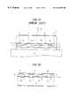
- FIG. 1Ais a schematic cross-sectional view of a prior art back surface point contact silicon solar cell having a double layer of metallization disclosed in U.S. Pat. No. 4, 927,770;
- FIG. 1Bis a view, similar to FIG. 1A, but showing a back surface point contact silicon solar cell having a double layer of metallization according to the invention
- FIG. 2is a process flow chart illustrating the process to fabricate the silicon solar cell (of FIG. 1B) according to the invention
- FIGS. 3A-3Hare sectional views of the silicon solar cell explaining the process shown in FIG. 2;
- FIGS. 3I-3Jare tables showing combination of metals to be used as the second metal layer (of FIG. 1B)
- FIG. 4is a view, similar to FIG. 2, but showing a process flow chart illustrating the process to fabricate the silicon solar cell (of FIG. 1B) according to a second embodiment of the invention
- FIGS. 5A-5Dare sectional views explaining the process shown in FIG. 4;
- FIG. 6is a view, similar to FIG. 2, but showing a process flow chart illustrating the process to fabricate the silicon solar cell (of FIG. 1B) according to a third embodiment of the invention
- FIG. 7is a table showing the comparison of characteristics of materials to be used in the insulator layer referred to in the process according to the third embodiment of the invention.
- FIGS. 8A-8Dare sectional views explaining the process shown in FIG. 6;
- FIG. 9is a view, similar to FIG. 2, but showing a process flow chart illustrating the process to fabricate the silicon solar cell (of FIG. 1B) according to a fourth embodiment of the invention.
- FIGS. 10A-10Bare sectional views explaining the process shown in FIG. 6;
- FIG. 11is a an enlarged view of portion A in FIG. 10B.
- FIG. 12is a schematic sectional view illustrating a problem occurred in the fabrication method described in the aforesaid U.S. patent.
- FIG. 1is a cross-sectional schematic view illustrating a back surface point contact silicon solar cell fabricated in the manner taught by U.S. Pat. No. 4,927,770, employing the double layer of metallization.
- the cellincludes a single-crystal silicon substrate 10 having a resistance of approximately 200 ⁇ -cm.
- the top surface of the substrate 10has a passivating layer 12 of silicon oxide, and the bottom surface includes alternating n-doped regions 14 and p-doped regions 16 .
- the bottom surface between the diffused regions 14 , 16is coated with a first passivating layer 18 of silicon oxide and a second passivating layer 20 of silicon nitrite (illustrated as a whole in the figure).
- the cellhas a first metal layer 24 , comprising sputtered aluminum for example, formed over the passivating layer to contact with the n-doped region 14 , an insulator (dielectric) layer 26 deposited on the first metal layer 24 and a second metal layer 28 made of a metal stack comprising aluminum and etc., deposited thereon to contact with the p-doped region 16 , as will later be explained in detail.
- a first metal layer 24comprising sputtered aluminum for example, formed over the passivating layer to contact with the n-doped region 14
- an insulator (dielectric) layer 26deposited on the first metal layer 24
- a second metal layer 28made of a metal stack comprising aluminum and etc., deposited thereon to contact with the p-doped region 16 , as will later be explained in detail.
- the solar cellis then mounted on a metallized substrate 100 through a solder layer 102 and a layer 104 . More specifically, the solar cell is soldered onto the contacts 104 of the metallized substrate 100 .
- the solar radiationis concentrated through a concentrator such as illustrated in U.S. Pat. No. 4,234,352 by ⁇ 200 to 500 (20 to 50 W/cm 2 ) and as shown in FIG. 1A, the concentrated solar radiation indicated by reference numeral 30 enters the silicon substrate 10 from the top surface and interacts with atoms of the silicon substrate 10 and forms electrons and holes which migrate to the n-doped and p-doped regions 14 , 16 respectively in the silicon substrate 10 and create voltage differentials between the doped regions 14 . The resulting voltage differentials are taken from the contacts 104 .
- the structure of the solar cell shown in FIG. 1Ais known and the gist of the invention resides in the fabrication of the same.
- the first metal layer 24is illustrated to come into contact with only the n-doped regions 14
- the second metal layer 28is shown to come into contact with only the p-doped regions 16 .
- the first metal layer 24is, in fact, brought into contact with both n-doped regions 14 and p-doped regions 16 and is patterned in such a way that the n-doped regions 14 and the p-doped regions 16 are isolated from each other.
- the second metal layer 28contacts the p-doped regions 16 by contacting the first metal layer 24 in regions where it contacts the p-doped regions 16 .
- FIG. 1Aonly shows the regions of the solar cell where only the p-doped regions 16 are contacted to the second metal layer 28 .
- FIG. 1Bthere are other regions of the cell where only the n-doped regions 14 are contacted to the second metal layer 28 a .
- the second metal layer 28is thus opened between these two regions by patterning it in such a way that no n-doped region 14 is contacted to a p-doped region 16 .
- FIG. 2is a process flow chart illustrating the process to fabricate the back surface contact point silicon solar cell (illustrated in FIG. 1B) according to the invention and FIG. 3A-3H are sectional views explaining the process shown in FIG. 2 . It should be noted here that the cell is turned bottom side up and the thicknesses and shape of portions are often deformed for illustration purpose in FIG. 3 A and on.
- the processbegins in S 10 in which, as shown in FIG. 3A, the silicon substrate 10 is deposited with the first passivating layer of silicon oxide 18 and is deposited with the second passivating layer of silicon nitride 20 on the top surface of layer 18 , while the substrate 10 is formed with the passivating layer 12 at its top. Then, opened windows 34 are formed through the first and second layers 18 , 20 to expose surface portions on the substrate 10 , and phosphorus-doped glass 36 is applied to the second layer 20 and into the opened windows 34 .
- a second plurality of opened windows 38are formed between the first opened windows and boron-doped glass 40 is applied over the surface and into the new opened windows 38 .
- the structureis then heated to a temperature of approximately 900° C. to 1150° C. such that dopants from the doped oxide layers (glasses) 36 , 40 diffuse into the surface of the substrate 10 to form the n-doped regions 14 and the p-doped region 16 .
- the substrateis then exposed to a silicon oxide etch to remove all of the exposed oxide layers (glasses) 36 , 40 to obtain the structure illustrated in FIG. 3 C.
- the processproceeds to S 14 in which the first metal layer 24 (e.g., sputtered aluminum) is deposited over the entire surface at the thickness of 2 to 4 ⁇ m to form contacts with all of the n-doped regions 14 and the p-doped region 16 as shown in FIG. 3 D.
- the first metal layer 24is then patterned and etched such that all of the doped regions 14 , 16 have separate contacts as shown in FIG. 3 E.
- the concentration ratioe.g., ⁇ 200 to 500, or incident power density of 20 to 50 W/cm 2
- the first metal layer 24is very thick (e.g., 2 to 4 ⁇ m).
- the high thickness of the first metal layer 24may sometimes make proper deposition of the second metal layer 28 (made of a metal stack at a thickness of 1 to 2 ⁇ m) over insulator layer 26 difficult, causing the second metal layer to have poor conductivityor worse, to break.
- this embodimentis configured to use a resilient organic material such as polyimide as the material for the insulator layer 26 .
- a resilient organic materialsuch as polyimide
- a thick layer of polyimidecan smooth the surface above the first metal layer 24 and make it more planar.
- the thick layer 26is liable to rise at the edges of the opened windows, rendering the second metal layer 28 to become too thin or worse, to break. Therefore, it is very important that the thick insulator layer 26 is patterned in such a way that the edges are not abrupt and have a round shape.
- the processproceeds to S 116 in which the thick layer 26 of polyimide (e.g., Hitachi PiX 3400 (trade mark)) is deposited over the first metal layer 24 to obtain a film thickness of approximately 5 ⁇ m, as shown in FIG. 3 F.
- polyimidee.g., Hitachi PiX 3400 (trade mark)
- the insulator layer 26is patterned to have opened windows 44 , as shown in FIG. 3 G. More specifically, a thin layer of photoresist (e.g., Shipley 1813 (trade mark)) is applied and the photoresist is exposed to ultraviolet through a photolithography mask (not shown). Then, the photoresist is developed using a developer (e.g., Shipley M319 (trade mark)). In the development, the polyimide is also etched. Then, a solvent (e.g., n-butyl acetate) is applied to remove the photoresist. In doing this, care should be taken not to remove the necessary polyimide portion. Other solvents such as cellosolve acetate could be used for the same purpose.
- a solvente.g., n-butyl acetate
- the processthen proceeds to S 18 in which the structure is heated in a furnace to cure the insulator layer 26 of polyimide. More specifically, the structure is baked or heated (in air or nitrogen atmosphere) at 120° C. for 30 minutes, followed by another 30 minutes at 200° C., and followed by still another 1 hour at 350° C.
- the processthen proceeds to S 20 in which the structure is additionally cured by being baked or heated (in air or nitrogen atmosphere) at an increased temperature up to 400° C. for 30 minutes. With this additional heating, the polyimide layer 26 is sufficiently cured and is contracted such that the edges at the opened windows 44 have round edges. In other words, the insulator layer 26 is relatively planarized and even.
- the temperature and time in the additional curing shown in S 20is an example that depends on the property or kind of the polyimide and the thickness of the insulator layer 26 .
- the inventorshave noted that increasing the time up to 1 hour at 400° C. was still effective for the purpose, but increasing the temperature to 500° C. made the insulator layer 26 too hard and resulted in cracking at the layer 26 .
- the processthen proceeds to S 22 in which the second metal layer 28 made of a metal stack (at the thickness of 1 to 2 ⁇ m) comprising aluminum/chromium/nickel /copper, is applied on the second insulator layer 26 b and the first metal layer 24 such that the aluminum layer in the second metal layer 28 and the first metal layer 24 comprising aluminum are joined together by being annealed to form contacts as shown in FIG. 3 H.
- annealingis, contrary to what is understood in the field of metallurgy, the process of heating the aluminum layers at a temperature of e.g., 350° C. to 400° C. to join them together.
- metal stackcomprising Al/Cr/Ni/Cu
- metal stackcomprising chromium/nickel/copper, or aluminum/titanium /nickel/silver, or aluminum/titanium/palladium/silver can be used.
- the metal stackcomprises an adhesion layer (innermost one to be adhered to the insulator layer 26 ) 1 , a diffusion barrier 2 and a solderable metal (outermost one) 3 , and as shown in FIG. 3I, any combination of metals from among the table can be used for them.
- the metal stackcomprises a light reflectivity enhancement (innermost) 1 , an adhesion layer 2 , a diffusion barrier 3 and a solderable layer 4 , and as shown in FIG. 3J, any combination can similarly be used.
- first metal layer 24is illustrated to come into contact with only the n-doped region, while the second metal layer 28 is shown to come into contact with only the p-doped region.
- the first and second metal layersare, in fact, brought into contact with the doped regions as illustrated in FIG. 3A etc.
- the method according to this embodimentcan present the back surface point contact silicon solar cell having a double layer of metallization, in which the cell surface to be soldered onto the metallized substrate 100 is well planarized and even to ensure sufficient conductibility, with less voids and less solder fatigue.
- FIG. 4is a view, similar to FIG. 2, but showing the method of fabricating a back surface point contact silicon solar cell according to a second embodiment of the invention.
- the single layer 26 of polyimide in the first embodimentis effective in planarizing the underlying topology created by the patterning of the first metal layer 24 .
- the single layer 26may sometimes create its own topology when it is in turn patterned to create the vias (conductors formed in the opened windows 44 in the insulator layer 26 ) for allowing the second metal layer 28 to come in contact with the first metal layer 24 in the selected locations.
- the inventorshave found that, by depositing two layers of polyimide with a reduced thickness, the cell surface can be better planarized while only creating a small step after patterning.
- the second embodimentaims to provide a method of fabricating a back surface point contact silicon solar cell with a higher level of planarization, even with very thick metallization.
- the processbegins in S 100 and proceeds, via S 102 , to S 104 in which the first metal layer 24 of 2 to 4 ⁇ m of aluminum is patterned, and then proceeds to S 106 in which a thick layer 26 a of polyimide (e.g., Hitachi PiX 3400 (trade mark)) is deposited to obtain a film thickness of approximately 2 to 4 ⁇ m. Then, after doing a pre-bake (pre-cure) to eliminate the solvents, the thick layer 26 a is patterned.
- polyimidee.g., Hitachi PiX 3400 (trade mark)
- a thin layer of photoresist(e.g., Shipley 1813 (trade mark)) is formed on the polyimide layer 26 and the photoresist is exposed to ultraviolet through a photolithography mask (not shown). Then, the photoresist is developed using a developer (e.g., Shipley M319 (trade mark)), while etching the polyimide. The patterning and etching are conducted in such a way that the polyimide film 26 a does not encroach (exceed) on top 240 of the first metal layer 24 , as shown in FIG. 5 A. Then, a solvent (e.g., n-butyl Acetate) is applied to remove the photoresist. In doing this, care should be taken not to remove the required pattern portion of polyimide. Other solvents such as cellosolve acetate could be used for the same purpose.
- a solvente.g., n-butyl Acetate
- the processthen proceeds to S 108 in which the structure is heated in a furnace to cure the insulator layer 26 a of polyimide. More specifically, the structure is baked or heated (in air or nitrogen atmosphere) at 120° C. for 30 minutes, followed by another 30 minutes at 200° C., and followed by still another 1 hour at 350° C.
- a second layer of polyimide 26 bis deposited over the first layer of polyimide 26 at a much higher speed.
- the material of the polyimide used in the second layer 26 bis the same as that of the first layer 26 a , but a less viscous polyimide is used to form a much thinner polyimide layer of approximately 1 ⁇ m.
- the second layer 26 bis then patterned and etched in the same way as the first layer 26 a , except that the second layer 26 b must encroach a little bit on top 240 of the first metal layer 24 .
- the first and second insulator layers 26 a , 26 bare patterned and etched to have the opened windows 44 as shown in FIG. 5 C.
- the processthen proceeds to S 114 in which the second metal layer 28 made of a metal stack (at the thickness of 1 to 2 ⁇ m) similar to that described in the first embodiment is applied on the second insulator layer 26 b and the first metal layer 24 such that the aluminum layer in the second metal layer 28 and the first metal layer 24 comprising aluminum are joined together by being annealed to form contacts as shown in FIG. 5 D.
- the polyimide applicationis made twice in the second embodiment, it makes easier to obtain the required thickness of the polyimide layer throughout the surface.
- a more planarized intermetal insulator surfaceis achieved with less raised edges.
- the planarized surfacealso improves the later soldering process with less voids, reduces the stress in the metallized substrate 100 and decreases the reliability problem of solder fatigue.
- FIG. 6is a view, similar to FIG. 2, but showing the method of fabricating a back surface point contact silicon solar cell according to a third embodiment of the invention.
- the third embodimentis an extension of the first embodiment or second embodiment, in which a double layer of silicon oxide and polyimide is used as the insulator intermetal layer such that the defects (drawbacks) of the materials are to a certain extent overcome.
- the oxide layerprovides a barrier against moisture that protects the first layer aluminum connections
- the polyimide layerprovides planarization and mechanical protection before the second metal layer deposition.
- itis effective to use such a double layer of an organic material (having resilience such as polyimide) and an inorganic material (such as silicon oxide) in obtaining a planarized surface better matched to the soldering base for the metallized substrate 100 .
- FIG. 7is a table showing the comparison of characteristics of the materials to be used in the insulator layer.
- the processbegins in S 200 and proceeds, via S 202 , to S 204 in which the first metal layer 24 of 2 to 4 ⁇ m aluminum is patterned, and proceeds to S 206 in which a first insulator layer 26 c of silicon oxide (SiO 2 ) is deposited over the first metal layer 24 to obtain a film thickness of approximately 1 ⁇ m, as shown in FIG. 8 A.
- S 204in which the first metal layer 24 of 2 to 4 ⁇ m aluminum is patterned
- S 206in which a first insulator layer 26 c of silicon oxide (SiO 2 ) is deposited over the first metal layer 24 to obtain a film thickness of approximately 1 ⁇ m, as shown in FIG. 8 A.
- the first insulator layer 26 cis patterned through photolithography to have the opened windows 44 therethrough, as shown in FIG. 8 B.
- the processthen proceeds to S 208 in which a second insulator layer of polyimide 26 d is deposited over the first layer of silicon oxide 26 c , as shown in FIG. 8C, to obtain a film thickness of approximately 2.5 ⁇ m. Then, the second layer of polyimide is patterned and etched through photolithography.
- the processproceeds to S 210 in which the structure is heated in a furnace to cure the second insulator layer of polyimide 26 d . More specifically, the structure is baked or heated (in air or nitrogen atmosphere) at 120° C. for 30 minutes, followed by another 30 minutes at 200° C., and followed by still another 1 hour at 350° C.
- the processthen proceeds to S 212 in which the second metal layer 28 made of a metal stack similar to that mentioned in the first embodiment is applied on the second insulator layer 26 d and the first metal layer 24 such that the aluminum layer in the second metal layer 28 and the first metal layer 24 comprising aluminum are joined together by being annealed to form contacts as shown in FIG. 8 D.
- Si 3 O 4 or SiOxNy or Al 2 O 3can be used for the first insulator layer 26 c , instead of SiO 2 .
- the double layer comprising the organic and inorganic material used in the third embodimentcan present a planarized surface better matched to the soldering base for the metallized substrate 100 .
- FIG. 9is a view, similar to FIG. 2, but showing the method of fabricating a back surface point contact silicon solar cell according to a fourth embodiment of the invention.
- the aluminum layersare annealed at 350° C. to 400° C. This sometimes causes topology (unevenness) to happen on the second metal layer 28 due to expansion of aluminum, making the deposition of chromium on the aluminum layer difficult, thereby degrading the conductivity.
- the second metal layeris made of a three-layer metal stack comprising materials other than aluminum, so as to provide a contact pad that can be easily soldered onto the metallized substrate 100 to obtain an improved conductivity.
- the processbegins in S 300 and proceeds, via S 302 , S 304 , to S 306 in which an insulator layer 26 e is applied using one of the first to third embodiments as shown in FIG. 10A, and proceeds to S 308 in which a second metal layer 28 c made of a three-layer of metal stack comprising a material other than aluminum, is applied on the insulator layer 26 e and the first metal layer 24 as shown in FIG. 10 B.
- the second metal layer 28 ccomprises a first layer 280 , a second layer 282 and a third layer 284 .
- the first layer 280comprises chromium (at the thickness of approximately 0.05 ⁇ m) and provides adhesion to the aluminum connectionsn the first metal layer 24 and to the insulator layer of polyimide.
- the second layer 282comprises nickel (at the thickness of approximately 0.2 to 0.4 ⁇ m) and acts as a diffusion barrier for the third layer 284 and for the solder.
- the third layer 284comprises copper (at the thickness of approximately 0.6 to 1.0 ⁇ m) which is solderable. The usage of copper has the advantage that it prevents the dissolving of nickel during the later solder process.
- the first layer 280is applied on the insulator 26 e through sputtering deposition, then the second layers 282 is applied on the first layer 280 through sputtering deposition, and then the third layer 284 is applied on the second layer 282 through sputtering deposition.
- first layer 280 , the second layer 282 and the third layer 284can be applied through sputtering or evaporation with shadow mask or using lift off technology or through deposition, followed by photolithography and etching.
- the three-layer metal stack used in the fourth embodimentcan provide a smooth planarized surface.
- the three-metal stack second layercan thus be applied with sufficient respective thicknesses, the structure is made robust, thereby improving the service life of the cell.
- the configurationcan also present better solderability for the metallized substrate.
- the substrate 10is coated with the first passivating layer 18 and the second passivating layer 20 , the second passivating layer 20 can be omitted.
Landscapes
- Photovoltaic Devices (AREA)
- Internal Circuitry In Semiconductor Integrated Circuit Devices (AREA)
Abstract
Description
Claims (4)
Priority Applications (2)
| Application Number | Priority Date | Filing Date | Title |
|---|---|---|---|
| US09/475,187US6423568B1 (en) | 1999-12-30 | 1999-12-30 | Method of fabricating a silicon solar cell |
| JP2000099303AJP2001189482A (en) | 1999-12-30 | 2000-03-31 | Method of manufacturing solar cell |
Applications Claiming Priority (1)
| Application Number | Priority Date | Filing Date | Title |
|---|---|---|---|
| US09/475,187US6423568B1 (en) | 1999-12-30 | 1999-12-30 | Method of fabricating a silicon solar cell |
Publications (1)
| Publication Number | Publication Date |
|---|---|
| US6423568B1true US6423568B1 (en) | 2002-07-23 |
Family
ID=23886560
Family Applications (1)
| Application Number | Title | Priority Date | Filing Date |
|---|---|---|---|
| US09/475,187Expired - LifetimeUS6423568B1 (en) | 1999-12-30 | 1999-12-30 | Method of fabricating a silicon solar cell |
Country Status (2)
| Country | Link |
|---|---|
| US (1) | US6423568B1 (en) |
| JP (1) | JP2001189482A (en) |
Cited By (108)
| Publication number | Priority date | Publication date | Assignee | Title |
|---|---|---|---|---|
| US20050022862A1 (en)* | 2003-08-01 | 2005-02-03 | Cudzinovic Michael J. | Methods and apparatus for fabricating solar cells |
| US20050022857A1 (en)* | 2003-08-01 | 2005-02-03 | Daroczi Shandor G. | Solar cell interconnect structure |
| US20050022861A1 (en)* | 2003-08-01 | 2005-02-03 | Rose Douglas H. | Etching of solar cell materials |
| US20050268959A1 (en)* | 2004-06-04 | 2005-12-08 | Sunpower Corporation | Interconnection of solar cells in a solar cell module |
| US6998288B1 (en) | 2003-10-03 | 2006-02-14 | Sunpower Corporation | Use of doped silicon dioxide in the fabrication of solar cells |
| US20060275936A1 (en)* | 2003-04-29 | 2006-12-07 | Pierre-Jean Ribeyron | Method for production of a semiconductor device with auto-aligned metallisations |
| US20070151598A1 (en)* | 2005-12-21 | 2007-07-05 | Denis De Ceuster | Back side contact solar cell structures and fabrication processes |
| DE102006007797A1 (en)* | 2006-02-20 | 2007-09-13 | Fraunhofer-Gesellschaft zur Förderung der angewandten Forschung e.V. | Semiconductor component and method for its production and its use |
| USD555084S1 (en) | 2005-11-18 | 2007-11-13 | Solaria Corporation | Circular solar cell package design |
| USD555083S1 (en) | 2005-11-08 | 2007-11-13 | Solaria Corporation | Solar cell package design |
| USD558139S1 (en) | 2005-11-18 | 2007-12-25 | Solaria Corporation | Triangular solar cell design |
| US20070295393A1 (en)* | 2004-05-18 | 2007-12-27 | Akeena Solar, Inc. | Mounting system for a solar panel |
| USD559174S1 (en) | 2005-11-18 | 2008-01-08 | Solaria Corporation | Shaped solar cell package design |
| US20080017243A1 (en)* | 2006-07-24 | 2008-01-24 | Denis De Ceuster | Solar cell with reduced base diffusion area |
| USD568238S1 (en) | 2005-11-18 | 2008-05-06 | Solaria Corporation | Rectangular solar cell package design |
| US20080134497A1 (en)* | 2006-12-11 | 2008-06-12 | Sunmodular, Inc. | Modular solar panels with heat exchange & methods of making thereof |
| US20080135086A1 (en)* | 2006-12-11 | 2008-06-12 | Sunmodular, Inc. | Photovoltaic cells, modules and methods of making same |
| US20080135090A1 (en)* | 2006-12-11 | 2008-06-12 | Sunmodular, Inc. | Solar roof tiles with heat exchange and methods of making thereof |
| US20080178922A1 (en)* | 2005-07-26 | 2008-07-31 | Solaria Corporation | Method and system for manufacturing solar panels using an integrated solar cell using a plurality of photovoltaic regions |
| US20080202577A1 (en)* | 2007-02-16 | 2008-08-28 | Henry Hieslmair | Dynamic design of solar cell structures, photovoltaic modules and corresponding processes |
| US20080236648A1 (en)* | 2007-03-30 | 2008-10-02 | Klein David L | Localized power point optimizer for solar cell installations |
| US20080236651A1 (en)* | 2007-04-02 | 2008-10-02 | Solaria Corporation | Solar cell concentrator structure including a plurality of concentrator elements with a notch design and method having a predetermined efficiency |
| US20080236664A1 (en)* | 2007-04-02 | 2008-10-02 | Solaria Corporation | Method and system for assembling a solar cell package |
| US20080299297A1 (en)* | 2007-05-29 | 2008-12-04 | Peter John Cousins | Array of small contacts for solar cell fabrication |
| US7468485B1 (en) | 2005-08-11 | 2008-12-23 | Sunpower Corporation | Back side contact solar cell with doped polysilicon regions |
| GB2451497A (en)* | 2007-07-31 | 2009-02-04 | Renewable Energy Corp Asa | Contact for solar cell |
| US20090032091A1 (en)* | 2007-08-03 | 2009-02-05 | Gigastorage Corporation | Solar cell |
| US20090056788A1 (en)* | 2007-09-05 | 2009-03-05 | Solaria Corporation | Notch structure for concentrating module and method of manufacture using photovoltaic strips |
| USD588534S1 (en) | 2007-07-26 | 2009-03-17 | Solaria Corporation | Shaped solar cell package |
| US20090078299A1 (en)* | 2007-09-21 | 2009-03-26 | Akeena Solar, Inc. | Mounting system for solar panels |
| USD591229S1 (en) | 2008-01-24 | 2009-04-28 | Solaria Corporation | Shaped solar cell package |
| US20090120487A1 (en)* | 2005-09-12 | 2009-05-14 | Solaria Corporation | Method and System for Assembling A Solar Cell Using a Plurality of Photovoltaic Regions |
| US20090151770A1 (en)* | 2007-12-12 | 2009-06-18 | Solaria Corporation | Method and material for coupling solar concentrators and photovoltaic devices |
| US20090151784A1 (en)* | 2007-12-14 | 2009-06-18 | Hsin-Chiao Luan | Anti-Reflective Coating With High Optical Absorption Layer For Backside Contact Solar Cells |
| US20090188563A1 (en)* | 2007-09-05 | 2009-07-30 | Solaria Corporation | Solar Cell Structure Including A Plurality of Concentrator Elements With A Notch Design and Predetermined Radii and Method |
| US20090205712A1 (en)* | 2008-02-20 | 2009-08-20 | Peter John Cousins | Front contact solar cell with formed emitter |
| US20090308457A1 (en)* | 2008-06-12 | 2009-12-17 | Smith David D | Trench Process And Structure For Backside Contact Solar Cells With Polysilicon Doped Regions |
| US20100000597A1 (en)* | 2008-07-01 | 2010-01-07 | Peter John Cousins | Front Contact Solar Cell With Formed Electrically Conducting Layers On the Front Side And Backside |
| WO2010015310A2 (en) | 2008-07-17 | 2010-02-11 | Fraunhofer- Gesellschaft Zur Förderung Der Angewandten Forschung E.V. | Solar cell and method for producing a solar cell |
| US20100078055A1 (en)* | 2005-08-22 | 2010-04-01 | Ruxandra Vidu | Nanostructure and photovoltaic cell implementing same |
| EP2190017A1 (en) | 2008-11-20 | 2010-05-26 | SAPHIRE ApS | High voltage semiconductor based wafer |
| US20100139745A1 (en)* | 2009-02-24 | 2010-06-10 | Peter John Cousins | Back Contact Sliver Cells |
| US20100144218A1 (en)* | 2006-08-25 | 2010-06-10 | Rose Douglas H | Solar cell interconnect with multiple current paths |
| US20100139764A1 (en)* | 2008-12-04 | 2010-06-10 | Smith David D | Backside Contact Solar Cell With Formed Polysilicon Doped Regions |
| GB2467361A (en)* | 2009-01-30 | 2010-08-04 | Renewable Energy Corp Asa | Contact and interconnect for a solar cell |
| US20100218800A1 (en)* | 2009-02-24 | 2010-09-02 | Peter John Cousins | Methods and Apparatus for Metallization of Solar Cells |
| US7790574B2 (en) | 2004-12-20 | 2010-09-07 | Georgia Tech Research Corporation | Boron diffusion in silicon devices |
| US20100282316A1 (en)* | 2007-04-02 | 2010-11-11 | Solaria Corporation | Solar Cell Concentrator Structure Including A Plurality of Glass Concentrator Elements With A Notch Design |
| US20100294352A1 (en)* | 2009-05-20 | 2010-11-25 | Uma Srinivasan | Metal patterning for electrically conductive structures based on alloy formation |
| US20100294349A1 (en)* | 2009-05-20 | 2010-11-25 | Uma Srinivasan | Back contact solar cells with effective and efficient designs and corresponding patterning processes |
| US20110000520A1 (en)* | 2009-07-02 | 2011-01-06 | West John R | Leveling foot apparatus, system, and method for photovoltaic arrays |
| US20110017263A1 (en)* | 2007-09-05 | 2011-01-27 | Solaria Corporation | Method and device for fabricating a solar cell using an interface pattern for a packaged design |
| US20110048505A1 (en)* | 2009-08-27 | 2011-03-03 | Gabriela Bunea | Module Level Solution to Solar Cell Polarization Using an Encapsulant with Opened UV Transmission Curve |
| US7910822B1 (en) | 2005-10-17 | 2011-03-22 | Solaria Corporation | Fabrication process for photovoltaic cell |
| US7910035B2 (en) | 2007-12-12 | 2011-03-22 | Solaria Corporation | Method and system for manufacturing integrated molded concentrator photovoltaic device |
| WO2011068480A1 (en)* | 2009-12-02 | 2011-06-09 | National University Of Singapore | Method and system for forming a metal electrode for a solar cell |
| US20110201188A1 (en)* | 2010-02-18 | 2011-08-18 | Varian Semiconductor Equipment Associates, Inc. | Self-aligned ion implantation for ibc solar cells |
| US20110214709A1 (en)* | 2010-03-03 | 2011-09-08 | Q1 Nanosystems Corporation | Nanostructure and photovoltaic cell implementing same |
| US20110220180A1 (en)* | 2007-09-21 | 2011-09-15 | Andalay Solar, Inc. | Electrical connectors for solar modules |
| US20110308591A1 (en)* | 2010-06-18 | 2011-12-22 | Semiconductor Energy Laboratory Co., Ltd. | Photoelectric Conversion Device and Manufacturing Method Thereof |
| US8119902B2 (en) | 2007-05-21 | 2012-02-21 | Solaria Corporation | Concentrating module and method of manufacture for photovoltaic strips |
| US8227688B1 (en) | 2005-10-17 | 2012-07-24 | Solaria Corporation | Method and resulting structure for assembling photovoltaic regions onto lead frame members for integration on concentrating elements for solar cells |
| US20120204926A1 (en)* | 2011-02-15 | 2012-08-16 | Gabriel Harley | Process and structures for fabrication of solar cells |
| US8350417B1 (en) | 2007-01-30 | 2013-01-08 | Sunpower Corporation | Method and apparatus for monitoring energy consumption of a customer structure |
| US8377738B2 (en) | 2010-07-01 | 2013-02-19 | Sunpower Corporation | Fabrication of solar cells with counter doping prevention |
| US8505248B1 (en) | 2007-09-21 | 2013-08-13 | Andalay Solar, Inc. | Minimal ballasted surface mounting system and method |
| US8513095B1 (en) | 2007-09-04 | 2013-08-20 | Solaria Corporation | Method and system for separating photovoltaic strips |
| USD699176S1 (en) | 2011-06-02 | 2014-02-11 | Solaria Corporation | Fastener for solar modules |
| US8707736B2 (en) | 2007-08-06 | 2014-04-29 | Solaria Corporation | Method and apparatus for manufacturing solar concentrators using glass process |
| US8786095B2 (en) | 2010-09-29 | 2014-07-22 | Sunpower Corporation | Interconnect for an optoelectronic device |
| US8796061B2 (en) | 2012-12-21 | 2014-08-05 | Sunpower Corporation | Module assembly for thin solar cells |
| US8822262B2 (en) | 2011-12-22 | 2014-09-02 | Sunpower Corporation | Fabricating solar cells with silicon nanoparticles |
| US8912083B2 (en) | 2011-01-31 | 2014-12-16 | Nanogram Corporation | Silicon substrates with doped surface contacts formed from doped silicon inks and corresponding processes |
| US8938932B1 (en)* | 2013-12-13 | 2015-01-27 | Quality Product Llc | Rail-less roof mounting system |
| US9035172B2 (en) | 2012-11-26 | 2015-05-19 | Sunpower Corporation | Crack resistant solar cell modules |
| US9076908B2 (en) | 2013-01-28 | 2015-07-07 | Q1 Nanosystems Corporation | Three-dimensional metamaterial device with photovoltaic bristles |
| US9154074B2 (en) | 2009-10-06 | 2015-10-06 | Solarcity Corporation | Apparatus for forming and mounting a photovoltaic array |
| US9243817B2 (en) | 2009-07-02 | 2016-01-26 | Solarcity Corporation | Apparatus for forming and mounting a photovoltaic array |
| USD749502S1 (en) | 2010-12-09 | 2016-02-16 | Solarcity Corporation | Combined panel skirt and photovoltaic panels |
| US9312406B2 (en) | 2012-12-19 | 2016-04-12 | Sunpower Corporation | Hybrid emitter all back contact solar cell |
| US9320926B2 (en) | 2012-06-28 | 2016-04-26 | Solarcity Corporation | Solar panel fire skirt |
| USD759464S1 (en) | 2010-07-02 | 2016-06-21 | Solarcity Corporation | Leveling foot |
| US20160247948A1 (en)* | 2015-02-19 | 2016-08-25 | Thomas P. Pass | Damage buffer for solar cell metallization |
| USD765591S1 (en) | 2011-12-09 | 2016-09-06 | Solarcity Corporation | Panel skirt and photovoltaic panel |
| US9461186B2 (en) | 2010-07-15 | 2016-10-04 | First Solar, Inc. | Back contact for a photovoltaic module |
| US9461192B2 (en)* | 2014-12-16 | 2016-10-04 | Sunpower Corporation | Thick damage buffer for foil-based metallization of solar cells |
| USD772432S1 (en) | 2010-07-02 | 2016-11-22 | Solarcity Corporation | Panel frame |
| US9518596B2 (en) | 2009-07-02 | 2016-12-13 | Solarcity Corporation | Pivot-fit frame, system and method for photovoltaic modules |
| US9685571B2 (en) | 2013-08-14 | 2017-06-20 | Sunpower Corporation | Solar cell module with high electric susceptibility layer |
| US9812590B2 (en) | 2012-10-25 | 2017-11-07 | Sunpower Corporation | Bifacial solar cell module with backside reflector |
| US9816731B2 (en) | 2010-07-02 | 2017-11-14 | Solarcity Corporation | Pivot-fit connection apparatus and system for photovoltaic arrays |
| US9947817B2 (en) | 2013-03-14 | 2018-04-17 | Q1 Nanosystems Corporation | Three-dimensional photovoltaic devices including non-conductive cores and methods of manufacture |
| US9954126B2 (en) | 2013-03-14 | 2018-04-24 | Q1 Nanosystems Corporation | Three-dimensional photovoltaic devices including cavity-containing cores and methods of manufacture |
| USD822890S1 (en) | 2016-09-07 | 2018-07-10 | Felxtronics Ap, Llc | Lighting apparatus |
| USD832495S1 (en) | 2017-08-18 | 2018-10-30 | Flex Ltd. | Lighting module locking mechanism |
| USD832494S1 (en) | 2017-08-09 | 2018-10-30 | Flex Ltd. | Lighting module heatsink |
| USD833061S1 (en) | 2017-08-09 | 2018-11-06 | Flex Ltd. | Lighting module locking endcap |
| USD846793S1 (en) | 2017-08-09 | 2019-04-23 | Flex Ltd. | Lighting module locking mechanism |
| USD862778S1 (en) | 2017-08-22 | 2019-10-08 | Flex Ltd | Lighting module lens |
| USD862777S1 (en) | 2017-08-09 | 2019-10-08 | Flex Ltd. | Lighting module wide distribution lens |
| USRE47733E1 (en) | 2004-02-05 | 2019-11-19 | Tesla, Inc. | Method and apparatus for mounting photovoltaic modules |
| USD872319S1 (en) | 2017-08-09 | 2020-01-07 | Flex Ltd. | Lighting module LED light board |
| USD877964S1 (en) | 2017-08-09 | 2020-03-10 | Flex Ltd. | Lighting module |
| US10636924B2 (en) | 2014-11-26 | 2020-04-28 | Sunpower Corporation | Solar module interconnect |
| US10676218B2 (en)* | 2016-05-23 | 2020-06-09 | Airbus Defence And Space Sas | Spacecraft |
| USD888323S1 (en) | 2017-09-07 | 2020-06-23 | Flex Ltd | Lighting module wire guard |
| US10775030B2 (en) | 2017-05-05 | 2020-09-15 | Flex Ltd. | Light fixture device including rotatable light modules |
| WO2024233301A1 (en)* | 2023-05-05 | 2024-11-14 | Georgia Tech Research Corporation | Silicon detector enabled by tunnel oxide passivating contact |
Citations (8)
| Publication number | Priority date | Publication date | Assignee | Title |
|---|---|---|---|---|
| US4234352A (en) | 1978-07-26 | 1980-11-18 | Electric Power Research Institute, Inc. | Thermophotovoltaic converter and cell for use therein |
| US4320251A (en)* | 1980-07-28 | 1982-03-16 | Solamat Inc. | Ohmic contacts for solar cells by arc plasma spraying |
| US4864016A (en)* | 1982-12-20 | 1989-09-05 | Hughes Aircraft Company | Polyimide composition and method for protecting photoreactive cells |
| US4927770A (en) | 1988-11-14 | 1990-05-22 | Electric Power Research Inst. Corp. Of District Of Columbia | Method of fabricating back surface point contact solar cells |
| US5282902A (en)* | 1991-05-09 | 1994-02-01 | Canon Kabushiki Kaisha | Solar cell provided with a light reflection layer |
| US5543333A (en)* | 1993-09-30 | 1996-08-06 | Siemens Solar Gmbh | Method for manufacturing a solar cell having combined metallization |
| US5591565A (en)* | 1992-03-20 | 1997-01-07 | Siemens Solar Gmbh | Solar cell with combined metallization and process for producing the same |
| US6107563A (en)* | 1997-10-27 | 2000-08-22 | Sharp Kabushiki Kaisha | Photoelectric converter having light diffusion layer |
Family Cites Families (9)
| Publication number | Priority date | Publication date | Assignee | Title |
|---|---|---|---|---|
| JPS6436083A (en)* | 1987-07-31 | 1989-02-07 | Matsushita Electric Industrial Co Ltd | Amorphous silicon solar cell |
| JPH0316184A (en)* | 1989-03-13 | 1991-01-24 | Fujitsu Ltd | Optical semiconductor device |
| JPH03257874A (en)* | 1990-03-07 | 1991-11-18 | Sanyo Electric Co Ltd | Manufacture of photoelectromotive device |
| JPH04255269A (en)* | 1991-02-07 | 1992-09-10 | Hitachi Ltd | Light receiving device |
| JPH04299581A (en)* | 1991-03-27 | 1992-10-22 | Taiyo Yuden Co Ltd | Manufacture of thin film element |
| JP2968404B2 (en)* | 1992-11-13 | 1999-10-25 | 三洋電機株式会社 | Method for manufacturing photovoltaic device |
| JP3029169B2 (en)* | 1993-05-07 | 2000-04-04 | キヤノン株式会社 | Photovoltaic element |
| JPH098340A (en)* | 1996-06-06 | 1997-01-10 | Canon Inc | Photovoltaic device and manufacturing method thereof |
| JPH11121800A (en)* | 1997-10-09 | 1999-04-30 | Fuji Electric Co Ltd | Group III nitride semiconductor device and method of manufacturing the same |
- 1999
- 1999-12-30USUS09/475,187patent/US6423568B1/ennot_activeExpired - Lifetime
- 2000
- 2000-03-31JPJP2000099303Apatent/JP2001189482A/enactivePending
Patent Citations (8)
| Publication number | Priority date | Publication date | Assignee | Title |
|---|---|---|---|---|
| US4234352A (en) | 1978-07-26 | 1980-11-18 | Electric Power Research Institute, Inc. | Thermophotovoltaic converter and cell for use therein |
| US4320251A (en)* | 1980-07-28 | 1982-03-16 | Solamat Inc. | Ohmic contacts for solar cells by arc plasma spraying |
| US4864016A (en)* | 1982-12-20 | 1989-09-05 | Hughes Aircraft Company | Polyimide composition and method for protecting photoreactive cells |
| US4927770A (en) | 1988-11-14 | 1990-05-22 | Electric Power Research Inst. Corp. Of District Of Columbia | Method of fabricating back surface point contact solar cells |
| US5282902A (en)* | 1991-05-09 | 1994-02-01 | Canon Kabushiki Kaisha | Solar cell provided with a light reflection layer |
| US5591565A (en)* | 1992-03-20 | 1997-01-07 | Siemens Solar Gmbh | Solar cell with combined metallization and process for producing the same |
| US5543333A (en)* | 1993-09-30 | 1996-08-06 | Siemens Solar Gmbh | Method for manufacturing a solar cell having combined metallization |
| US6107563A (en)* | 1997-10-27 | 2000-08-22 | Sharp Kabushiki Kaisha | Photoelectric converter having light diffusion layer |
Cited By (213)
| Publication number | Priority date | Publication date | Assignee | Title |
|---|---|---|---|---|
| US7364938B2 (en)* | 2003-04-29 | 2008-04-29 | Commissariat A L'energie Atomique | Method for production of a semiconductor device with auto-aligned metallisations |
| US20060275936A1 (en)* | 2003-04-29 | 2006-12-07 | Pierre-Jean Ribeyron | Method for production of a semiconductor device with auto-aligned metallisations |
| CN100452442C (en)* | 2003-04-29 | 2009-01-14 | 法国原子能委员会 | Method for production of a semiconductor device with auto-aligned metallisations |
| US20090042330A1 (en)* | 2003-08-01 | 2009-02-12 | Sunpower Corporation | Etching Of Solar Cell Materials |
| US20090039312A1 (en)* | 2003-08-01 | 2009-02-12 | Sunpower Corporation | Etching Of Solar Cell Materials |
| US8029683B2 (en) | 2003-08-01 | 2011-10-04 | Sunpower Corporation | Etching of solar cell materials |
| US7455787B2 (en) | 2003-08-01 | 2008-11-25 | Sunpower Corporation | Etching of solar cell materials |
| US20050022862A1 (en)* | 2003-08-01 | 2005-02-03 | Cudzinovic Michael J. | Methods and apparatus for fabricating solar cells |
| US20050022861A1 (en)* | 2003-08-01 | 2005-02-03 | Rose Douglas H. | Etching of solar cell materials |
| US20050022857A1 (en)* | 2003-08-01 | 2005-02-03 | Daroczi Shandor G. | Solar cell interconnect structure |
| US6998288B1 (en) | 2003-10-03 | 2006-02-14 | Sunpower Corporation | Use of doped silicon dioxide in the fabrication of solar cells |
| USRE47733E1 (en) | 2004-02-05 | 2019-11-19 | Tesla, Inc. | Method and apparatus for mounting photovoltaic modules |
| US20070295393A1 (en)* | 2004-05-18 | 2007-12-27 | Akeena Solar, Inc. | Mounting system for a solar panel |
| US7987641B2 (en) | 2004-05-18 | 2011-08-02 | Andalay Solar, Inc. | Mounting system for a solar panel |
| US7390961B2 (en) | 2004-06-04 | 2008-06-24 | Sunpower Corporation | Interconnection of solar cells in a solar cell module |
| US20050268959A1 (en)* | 2004-06-04 | 2005-12-08 | Sunpower Corporation | Interconnection of solar cells in a solar cell module |
| US7790574B2 (en) | 2004-12-20 | 2010-09-07 | Georgia Tech Research Corporation | Boron diffusion in silicon devices |
| US20080236740A1 (en)* | 2005-07-26 | 2008-10-02 | Solaria Corporation | Method and system for manufacturing solar panels using an integrated solar cell using a plurality of photovoltaic regions |
| US20080178922A1 (en)* | 2005-07-26 | 2008-07-31 | Solaria Corporation | Method and system for manufacturing solar panels using an integrated solar cell using a plurality of photovoltaic regions |
| US7468485B1 (en) | 2005-08-11 | 2008-12-23 | Sunpower Corporation | Back side contact solar cell with doped polysilicon regions |
| US7633006B1 (en) | 2005-08-11 | 2009-12-15 | Sunpower Corporation | Back side contact solar cell with doped polysilicon regions |
| US20110036395A1 (en)* | 2005-08-22 | 2011-02-17 | The Regents Of The University Of California | Methods for forming nanostructures and photovoltaic cells implementing same |
| US8906733B2 (en) | 2005-08-22 | 2014-12-09 | Q1 Nanosystems, Inc. | Methods for forming nanostructures and photovoltaic cells implementing same |
| US20100078055A1 (en)* | 2005-08-22 | 2010-04-01 | Ruxandra Vidu | Nanostructure and photovoltaic cell implementing same |
| US8344241B1 (en) | 2005-08-22 | 2013-01-01 | Q1 Nanosystems Corporation | Nanostructure and photovoltaic cell implementing same |
| US8877541B2 (en) | 2005-08-22 | 2014-11-04 | Q1 Nanosystems, Inc. | Nanostructure and photovoltaic cell implementing same |
| US7847180B2 (en) | 2005-08-22 | 2010-12-07 | Q1 Nanosystems, Inc. | Nanostructure and photovoltaic cell implementing same |
| US20090120487A1 (en)* | 2005-09-12 | 2009-05-14 | Solaria Corporation | Method and System for Assembling A Solar Cell Using a Plurality of Photovoltaic Regions |
| US7910822B1 (en) | 2005-10-17 | 2011-03-22 | Solaria Corporation | Fabrication process for photovoltaic cell |
| US8227688B1 (en) | 2005-10-17 | 2012-07-24 | Solaria Corporation | Method and resulting structure for assembling photovoltaic regions onto lead frame members for integration on concentrating elements for solar cells |
| USD555083S1 (en) | 2005-11-08 | 2007-11-13 | Solaria Corporation | Solar cell package design |
| USD568238S1 (en) | 2005-11-18 | 2008-05-06 | Solaria Corporation | Rectangular solar cell package design |
| USD559174S1 (en) | 2005-11-18 | 2008-01-08 | Solaria Corporation | Shaped solar cell package design |
| USD558139S1 (en) | 2005-11-18 | 2007-12-25 | Solaria Corporation | Triangular solar cell design |
| USD555084S1 (en) | 2005-11-18 | 2007-11-13 | Solaria Corporation | Circular solar cell package design |
| US8163638B2 (en) | 2005-12-21 | 2012-04-24 | Sunpower Corporation | Back side contact solar cell structures and fabrication processes |
| US8409912B2 (en) | 2005-12-21 | 2013-04-02 | Sunpower Corporation | Back side contact solar cell structures and fabrication processes |
| US7820475B2 (en)* | 2005-12-21 | 2010-10-26 | Sunpower Corporation | Back side contact solar cell structures and fabrication processes |
| US20070151598A1 (en)* | 2005-12-21 | 2007-07-05 | Denis De Ceuster | Back side contact solar cell structures and fabrication processes |
| US20110000540A1 (en)* | 2005-12-21 | 2011-01-06 | Denis De Ceuster | Back Side Contact Solar Cell Structures And Fabrication Processes |
| US20110003424A1 (en)* | 2005-12-21 | 2011-01-06 | Denis De Ceuster | Back Side Contact Solar Cell Structures And Fabrication Processes |
| US20090032095A1 (en)* | 2006-02-20 | 2009-02-05 | Fraunhofer-Gesellschaft Zur Forderung Der Angewandten Forschung E.V. | Semiconductor Component And Method For Producing It and Use for It |
| DE102006007797A1 (en)* | 2006-02-20 | 2007-09-13 | Fraunhofer-Gesellschaft zur Förderung der angewandten Forschung e.V. | Semiconductor component and method for its production and its use |
| DE102006007797B4 (en)* | 2006-02-20 | 2008-01-03 | Fraunhofer-Gesellschaft zur Förderung der angewandten Forschung e.V. | Method for producing a semiconductor component and its use |
| US8664519B2 (en) | 2006-07-24 | 2014-03-04 | Sunpower Corporation | Solar cell with reduced base diffusion area |
| US8008575B2 (en) | 2006-07-24 | 2011-08-30 | Sunpower Corporation | Solar cell with reduced base diffusion area |
| US20080017243A1 (en)* | 2006-07-24 | 2008-01-24 | Denis De Ceuster | Solar cell with reduced base diffusion area |
| US9691924B1 (en) | 2006-08-25 | 2017-06-27 | Sunpower Corporation | Solar cell interconnect with multiple current paths |
| US8148627B2 (en) | 2006-08-25 | 2012-04-03 | Sunpower Corporation | Solar cell interconnect with multiple current paths |
| US20100144218A1 (en)* | 2006-08-25 | 2010-06-10 | Rose Douglas H | Solar cell interconnect with multiple current paths |
| US20080135090A1 (en)* | 2006-12-11 | 2008-06-12 | Sunmodular, Inc. | Solar roof tiles with heat exchange and methods of making thereof |
| US8410350B2 (en) | 2006-12-11 | 2013-04-02 | Ns Acquisition Llc | Modular solar panels with heat exchange |
| US20080134497A1 (en)* | 2006-12-11 | 2008-06-12 | Sunmodular, Inc. | Modular solar panels with heat exchange & methods of making thereof |
| US20080135086A1 (en)* | 2006-12-11 | 2008-06-12 | Sunmodular, Inc. | Photovoltaic cells, modules and methods of making same |
| US20080135088A1 (en)* | 2006-12-11 | 2008-06-12 | Sunmodular, Inc. | Interlocking solar roof tiles with heat exchange |
| US20080135094A1 (en)* | 2006-12-11 | 2008-06-12 | Sunmodular, Inc. | Photovoltaic roof tiles and methods of making same |
| US7728219B2 (en) | 2006-12-11 | 2010-06-01 | Sunmodular, Inc. | Photovoltaic cells, modules and methods of making same |
| US8350417B1 (en) | 2007-01-30 | 2013-01-08 | Sunpower Corporation | Method and apparatus for monitoring energy consumption of a customer structure |
| EP2654089A2 (en) | 2007-02-16 | 2013-10-23 | Nanogram Corporation | Solar cell structures, photovoltaic modules and corresponding processes |
| US8853527B2 (en) | 2007-02-16 | 2014-10-07 | Nanogram Corporation | Solar cell structures, photovoltaic panels and corresponding processes |
| US20080202577A1 (en)* | 2007-02-16 | 2008-08-28 | Henry Hieslmair | Dynamic design of solar cell structures, photovoltaic modules and corresponding processes |
| US9343606B2 (en) | 2007-02-16 | 2016-05-17 | Nanogram Corporation | Solar cell structures, photovoltaic panels and corresponding processes |
| US20080202576A1 (en)* | 2007-02-16 | 2008-08-28 | Henry Hieslmair | Solar cell structures, photovoltaic panels and corresponding processes |
| US8409976B2 (en) | 2007-02-16 | 2013-04-02 | Nanogram Corporation | Solar cell structures, photovoltaic panels and corresponding processes |
| US9281419B2 (en) | 2007-03-30 | 2016-03-08 | Sunpower Corporation | Localized power point optimizer for solar cell installations |
| US20080236648A1 (en)* | 2007-03-30 | 2008-10-02 | Klein David L | Localized power point optimizer for solar cell installations |
| US8158877B2 (en) | 2007-03-30 | 2012-04-17 | Sunpower Corporation | Localized power point optimizer for solar cell installations |
| US20080236651A1 (en)* | 2007-04-02 | 2008-10-02 | Solaria Corporation | Solar cell concentrator structure including a plurality of concentrator elements with a notch design and method having a predetermined efficiency |
| US20100282316A1 (en)* | 2007-04-02 | 2010-11-11 | Solaria Corporation | Solar Cell Concentrator Structure Including A Plurality of Glass Concentrator Elements With A Notch Design |
| US20080236664A1 (en)* | 2007-04-02 | 2008-10-02 | Solaria Corporation | Method and system for assembling a solar cell package |
| US7910392B2 (en) | 2007-04-02 | 2011-03-22 | Solaria Corporation | Method and system for assembling a solar cell package |
| US20110000526A1 (en)* | 2007-04-06 | 2011-01-06 | West John R | Pivot-fit frame, system and method for photovoltaic modules |
| US8919052B2 (en) | 2007-04-06 | 2014-12-30 | Zep Solar, Llc | Pivot-fit frame, system and method for photovoltaic modules |
| US8119902B2 (en) | 2007-05-21 | 2012-02-21 | Solaria Corporation | Concentrating module and method of manufacture for photovoltaic strips |
| WO2008150344A1 (en)* | 2007-05-29 | 2008-12-11 | Sunpower Corporation | Array of small contacts for solar cell fabrication |
| US20110061731A1 (en)* | 2007-05-29 | 2011-03-17 | Peter John Cousins | Array Of Small Contacts For Solar Cell Fabrication |
| US20080299297A1 (en)* | 2007-05-29 | 2008-12-04 | Peter John Cousins | Array of small contacts for solar cell fabrication |
| AU2008260627B2 (en)* | 2007-05-29 | 2013-08-15 | Maxeon Solar Pte. Ltd. | Array of small contacts for solar cell fabrication |
| KR101384498B1 (en) | 2007-05-29 | 2014-04-14 | 선파워 코포레이션 | Array of small contacts for solar cell fabrication |
| US8883247B2 (en)* | 2007-05-29 | 2014-11-11 | Sunpower Corporation | Array of small contacts for solar cell fabrication |
| US7838062B2 (en) | 2007-05-29 | 2010-11-23 | Sunpower Corporation | Array of small contacts for solar cell fabrication |
| CN101681902B (en)* | 2007-05-29 | 2012-07-04 | 太阳能公司 | Array of small contacts for solar cell fabrication |
| USD588534S1 (en) | 2007-07-26 | 2009-03-17 | Solaria Corporation | Shaped solar cell package |
| WO2009017420A3 (en)* | 2007-07-31 | 2009-08-13 | Renewable Energy Corp Asa | Method for providing a contact on the back surface of a solar cell, and a solar cell with contacts provided according to the method |
| GB2451497A (en)* | 2007-07-31 | 2009-02-04 | Renewable Energy Corp Asa | Contact for solar cell |
| US20090032091A1 (en)* | 2007-08-03 | 2009-02-05 | Gigastorage Corporation | Solar cell |
| US8707736B2 (en) | 2007-08-06 | 2014-04-29 | Solaria Corporation | Method and apparatus for manufacturing solar concentrators using glass process |
| US8513095B1 (en) | 2007-09-04 | 2013-08-20 | Solaria Corporation | Method and system for separating photovoltaic strips |
| US20110017263A1 (en)* | 2007-09-05 | 2011-01-27 | Solaria Corporation | Method and device for fabricating a solar cell using an interface pattern for a packaged design |
| US20090188563A1 (en)* | 2007-09-05 | 2009-07-30 | Solaria Corporation | Solar Cell Structure Including A Plurality of Concentrator Elements With A Notch Design and Predetermined Radii and Method |
| US20090056788A1 (en)* | 2007-09-05 | 2009-03-05 | Solaria Corporation | Notch structure for concentrating module and method of manufacture using photovoltaic strips |
| US8049098B2 (en) | 2007-09-05 | 2011-11-01 | Solaria Corporation | Notch structure for concentrating module and method of manufacture using photovoltaic strips |
| US8505248B1 (en) | 2007-09-21 | 2013-08-13 | Andalay Solar, Inc. | Minimal ballasted surface mounting system and method |
| US20110220180A1 (en)* | 2007-09-21 | 2011-09-15 | Andalay Solar, Inc. | Electrical connectors for solar modules |
| US8813460B2 (en) | 2007-09-21 | 2014-08-26 | Andalay Solar, Inc. | Mounting system for solar panels |
| US20090078299A1 (en)* | 2007-09-21 | 2009-03-26 | Akeena Solar, Inc. | Mounting system for solar panels |
| US8938919B2 (en) | 2007-09-21 | 2015-01-27 | Andalay Solar, Inc. | Electrical connectors for solar modules |
| US7910035B2 (en) | 2007-12-12 | 2011-03-22 | Solaria Corporation | Method and system for manufacturing integrated molded concentrator photovoltaic device |
| US20090151770A1 (en)* | 2007-12-12 | 2009-06-18 | Solaria Corporation | Method and material for coupling solar concentrators and photovoltaic devices |
| US8748736B2 (en) | 2007-12-14 | 2014-06-10 | Sunpower Corporation | Anti-reflective coating with high optical absorption layer for backside contact solar cells |
| US20090151784A1 (en)* | 2007-12-14 | 2009-06-18 | Hsin-Chiao Luan | Anti-Reflective Coating With High Optical Absorption Layer For Backside Contact Solar Cells |
| US8198528B2 (en) | 2007-12-14 | 2012-06-12 | Sunpower Corporation | Anti-reflective coating with high optical absorption layer for backside contact solar cells |
| USD591229S1 (en) | 2008-01-24 | 2009-04-28 | Solaria Corporation | Shaped solar cell package |
| US20090205712A1 (en)* | 2008-02-20 | 2009-08-20 | Peter John Cousins | Front contact solar cell with formed emitter |
| US8878053B2 (en) | 2008-02-20 | 2014-11-04 | Sunpower Corporation | Front contact solar cell with formed emitter |
| US8222516B2 (en) | 2008-02-20 | 2012-07-17 | Sunpower Corporation | Front contact solar cell with formed emitter |
| US9496821B2 (en) | 2008-04-08 | 2016-11-15 | Solarcity Corporation | Method and apparatus for forming and mounting a photovoltaic array |
| US10396230B2 (en)* | 2008-06-12 | 2019-08-27 | Sunpower Corporation | Backside contact solar cells with separated polysilicon doped regions |
| US20090308438A1 (en)* | 2008-06-12 | 2009-12-17 | Denis De Ceuster | Trench Process and Structure for Backside Contact Solar Cells with Polysilicon Doped Regions |
| US20090308457A1 (en)* | 2008-06-12 | 2009-12-17 | Smith David D | Trench Process And Structure For Backside Contact Solar Cells With Polysilicon Doped Regions |
| US20110003423A1 (en)* | 2008-06-12 | 2011-01-06 | Smith David D | Trench Process And Structure For Backside Contact Solar Cells With Polysilicon Doped Regions |
| US20110059571A1 (en)* | 2008-06-12 | 2011-03-10 | Denis De Ceuster | Trench Process and Structure for Backside Contact Solar Cells with Polysilicon Doped Regions |
| US7851698B2 (en)* | 2008-06-12 | 2010-12-14 | Sunpower Corporation | Trench process and structure for backside contact solar cells with polysilicon doped regions |
| US8460963B2 (en) | 2008-06-12 | 2013-06-11 | Sunpower Corporation | Trench process and structure for backside contact solar cells with polysilicon doped regions |
| US7812250B2 (en)* | 2008-06-12 | 2010-10-12 | Sunpower Corporation | Trench process and structure for backside contact solar cells with polysilicon doped regions |
| US8450134B2 (en) | 2008-06-12 | 2013-05-28 | Sunpower Corporation | Trench process and structure for backside contact solar cells with polysilicon doped regions |
| US20100000597A1 (en)* | 2008-07-01 | 2010-01-07 | Peter John Cousins | Front Contact Solar Cell With Formed Electrically Conducting Layers On the Front Side And Backside |
| US8207444B2 (en) | 2008-07-01 | 2012-06-26 | Sunpower Corporation | Front contact solar cell with formed electrically conducting layers on the front side and backside |
| US9437755B2 (en) | 2008-07-01 | 2016-09-06 | Sunpower Corporation | Front contact solar cell with formed electrically conducting layers on the front side and backside |
| US20110139241A1 (en)* | 2008-07-17 | 2011-06-16 | Fraunhofer-Gesellschaft Zur Forderung Der Angewandten Forschung E.V. | Solar cell and method for producing a solar cell |
| WO2010015310A2 (en) | 2008-07-17 | 2010-02-11 | Fraunhofer- Gesellschaft Zur Förderung Der Angewandten Forschung E.V. | Solar cell and method for producing a solar cell |
| WO2010015310A3 (en)* | 2008-07-17 | 2010-06-17 | Fraunhofer- Gesellschaft Zur Förderung Der Angewandten Forschung E.V. | Solar cell and method for producing a solar cell |
| EP2190017A1 (en) | 2008-11-20 | 2010-05-26 | SAPHIRE ApS | High voltage semiconductor based wafer |
| US8242354B2 (en) | 2008-12-04 | 2012-08-14 | Sunpower Corporation | Backside contact solar cell with formed polysilicon doped regions |
| US20100139764A1 (en)* | 2008-12-04 | 2010-06-10 | Smith David D | Backside Contact Solar Cell With Formed Polysilicon Doped Regions |
| CN102362366B (en)* | 2009-01-30 | 2013-11-20 | 可再生能源公司 | Back contacting and interconnection of two solar cells |
| GB2467361A (en)* | 2009-01-30 | 2010-08-04 | Renewable Energy Corp Asa | Contact and interconnect for a solar cell |
| US8409911B2 (en) | 2009-02-24 | 2013-04-02 | Sunpower Corporation | Methods for metallization of solar cells |
| US20100139745A1 (en)* | 2009-02-24 | 2010-06-10 | Peter John Cousins | Back Contact Sliver Cells |
| US9070804B2 (en) | 2009-02-24 | 2015-06-30 | Sunpower Corporation | Back contact sliver cells |
| US20100218800A1 (en)* | 2009-02-24 | 2010-09-02 | Peter John Cousins | Methods and Apparatus for Metallization of Solar Cells |
| US20100294349A1 (en)* | 2009-05-20 | 2010-11-25 | Uma Srinivasan | Back contact solar cells with effective and efficient designs and corresponding patterning processes |
| US20100294352A1 (en)* | 2009-05-20 | 2010-11-25 | Uma Srinivasan | Metal patterning for electrically conductive structures based on alloy formation |
| US9447801B2 (en) | 2009-07-02 | 2016-09-20 | Solarcity Corporation | Apparatus for forming and mounting a photovoltaic array |
| US9831818B2 (en) | 2009-07-02 | 2017-11-28 | Solarcity Corporation | Pivot-fit frame, system and method for photovoltaic modules |
| US9243817B2 (en) | 2009-07-02 | 2016-01-26 | Solarcity Corporation | Apparatus for forming and mounting a photovoltaic array |
| US20110000544A1 (en)* | 2009-07-02 | 2011-01-06 | West John R | Drop-in connection apparatus, system, and method for photovoltaic arrays |
| US20110000519A1 (en)* | 2009-07-02 | 2011-01-06 | West John R | Pivot-fit connection apparatus, system, and method for photovoltaic modules |
| US20110000520A1 (en)* | 2009-07-02 | 2011-01-06 | West John R | Leveling foot apparatus, system, and method for photovoltaic arrays |
| US9518596B2 (en) | 2009-07-02 | 2016-12-13 | Solarcity Corporation | Pivot-fit frame, system and method for photovoltaic modules |
| US9853597B2 (en) | 2009-07-02 | 2017-12-26 | Solarcity Corporation | Pivot-fit connection apparatus, system, and method for photovoltaic modules |
| US8919053B2 (en) | 2009-07-02 | 2014-12-30 | Zep Solar, Llc | Leveling foot apparatus, system, and method for photovoltaic arrays |
| US8991114B2 (en) | 2009-07-02 | 2015-03-31 | Zep Solar, Llc | Pivot-fit connection apparatus, system, and method for photovoltaic modules |
| US9599280B2 (en) | 2009-07-02 | 2017-03-21 | Solarcity Corporation | Pivot-fit frame, system and method for photovoltaic modules |
| US9574588B2 (en) | 2009-07-02 | 2017-02-21 | Solarcity Corporation | Method and apparatus for forming and mounting a photovoltaic array |
| US20110048505A1 (en)* | 2009-08-27 | 2011-03-03 | Gabriela Bunea | Module Level Solution to Solar Cell Polarization Using an Encapsulant with Opened UV Transmission Curve |
| US9154074B2 (en) | 2009-10-06 | 2015-10-06 | Solarcity Corporation | Apparatus for forming and mounting a photovoltaic array |
| US9300244B2 (en) | 2009-10-06 | 2016-03-29 | Solarcity Corporation | Apparatus for forming and mounting a photovoltaic array |
| WO2011068480A1 (en)* | 2009-12-02 | 2011-06-09 | National University Of Singapore | Method and system for forming a metal electrode for a solar cell |
| US20110201188A1 (en)* | 2010-02-18 | 2011-08-18 | Varian Semiconductor Equipment Associates, Inc. | Self-aligned ion implantation for ibc solar cells |
| US8735234B2 (en) | 2010-02-18 | 2014-05-27 | Varian Semiconductor Equipment Associates, Inc. | Self-aligned ion implantation for IBC solar cells |
| US9202954B2 (en) | 2010-03-03 | 2015-12-01 | Q1 Nanosystems Corporation | Nanostructure and photovoltaic cell implementing same |
| US20110214709A1 (en)* | 2010-03-03 | 2011-09-08 | Q1 Nanosystems Corporation | Nanostructure and photovoltaic cell implementing same |
| US8816194B2 (en)* | 2010-06-18 | 2014-08-26 | Semiconductor Energy Laboratory Co., Ltd. | Photoelectric conversion device and manufacturing method thereof |
| US9099579B2 (en) | 2010-06-18 | 2015-08-04 | Semiconductor Energy Laboratory Co., Ltd. | Photoelectric conversion device and manufacturing method thereof |
| US20110308591A1 (en)* | 2010-06-18 | 2011-12-22 | Semiconductor Energy Laboratory Co., Ltd. | Photoelectric Conversion Device and Manufacturing Method Thereof |
| US8377738B2 (en) | 2010-07-01 | 2013-02-19 | Sunpower Corporation | Fabrication of solar cells with counter doping prevention |
| USD812457S1 (en) | 2010-07-02 | 2018-03-13 | Solarcity Corporation | Coupling |
| USD817741S1 (en) | 2010-07-02 | 2018-05-15 | Solarcity Corporation | Leveling foot |
| USD759464S1 (en) | 2010-07-02 | 2016-06-21 | Solarcity Corporation | Leveling foot |
| US9816731B2 (en) | 2010-07-02 | 2017-11-14 | Solarcity Corporation | Pivot-fit connection apparatus and system for photovoltaic arrays |
| USD772432S1 (en) | 2010-07-02 | 2016-11-22 | Solarcity Corporation | Panel frame |
| US9461186B2 (en) | 2010-07-15 | 2016-10-04 | First Solar, Inc. | Back contact for a photovoltaic module |
| US8786095B2 (en) | 2010-09-29 | 2014-07-22 | Sunpower Corporation | Interconnect for an optoelectronic device |
| US9537036B2 (en) | 2010-09-29 | 2017-01-03 | Sunpower Corporation | Interconnect for an optoelectronic device |
| US9291369B2 (en) | 2010-12-09 | 2016-03-22 | Solarcity Corporation | Skirt for photovoltaic arrays |
| USD749502S1 (en) | 2010-12-09 | 2016-02-16 | Solarcity Corporation | Combined panel skirt and photovoltaic panels |
| US8912083B2 (en) | 2011-01-31 | 2014-12-16 | Nanogram Corporation | Silicon substrates with doped surface contacts formed from doped silicon inks and corresponding processes |
| US9378957B2 (en) | 2011-01-31 | 2016-06-28 | Nanogram Corporation | Silicon substrates with doped surface contacts formed from doped silicon based inks and corresponding processes |
| US20120204926A1 (en)* | 2011-02-15 | 2012-08-16 | Gabriel Harley | Process and structures for fabrication of solar cells |
| US8586403B2 (en)* | 2011-02-15 | 2013-11-19 | Sunpower Corporation | Process and structures for fabrication of solar cells with laser ablation steps to form contact holes |
| USD699176S1 (en) | 2011-06-02 | 2014-02-11 | Solaria Corporation | Fastener for solar modules |
| USD765591S1 (en) | 2011-12-09 | 2016-09-06 | Solarcity Corporation | Panel skirt and photovoltaic panel |
| US8822262B2 (en) | 2011-12-22 | 2014-09-02 | Sunpower Corporation | Fabricating solar cells with silicon nanoparticles |
| US9320926B2 (en) | 2012-06-28 | 2016-04-26 | Solarcity Corporation | Solar panel fire skirt |
| US9812590B2 (en) | 2012-10-25 | 2017-11-07 | Sunpower Corporation | Bifacial solar cell module with backside reflector |
| US9035172B2 (en) | 2012-11-26 | 2015-05-19 | Sunpower Corporation | Crack resistant solar cell modules |
| US9312406B2 (en) | 2012-12-19 | 2016-04-12 | Sunpower Corporation | Hybrid emitter all back contact solar cell |
| US8796061B2 (en) | 2012-12-21 | 2014-08-05 | Sunpower Corporation | Module assembly for thin solar cells |
| US9082911B2 (en) | 2013-01-28 | 2015-07-14 | Q1 Nanosystems Corporation | Three-dimensional metamaterial device with photovoltaic bristles |
| US9076908B2 (en) | 2013-01-28 | 2015-07-07 | Q1 Nanosystems Corporation | Three-dimensional metamaterial device with photovoltaic bristles |
| US9947817B2 (en) | 2013-03-14 | 2018-04-17 | Q1 Nanosystems Corporation | Three-dimensional photovoltaic devices including non-conductive cores and methods of manufacture |
| US9954126B2 (en) | 2013-03-14 | 2018-04-24 | Q1 Nanosystems Corporation | Three-dimensional photovoltaic devices including cavity-containing cores and methods of manufacture |
| US9685571B2 (en) | 2013-08-14 | 2017-06-20 | Sunpower Corporation | Solar cell module with high electric susceptibility layer |
| US8938932B1 (en)* | 2013-12-13 | 2015-01-27 | Quality Product Llc | Rail-less roof mounting system |
| US11784270B2 (en) | 2014-11-26 | 2023-10-10 | Maxeon Solar Pte. Ltd. | Solar module interconnect |
| US10636924B2 (en) | 2014-11-26 | 2020-04-28 | Sunpower Corporation | Solar module interconnect |
| US10199521B2 (en) | 2014-12-16 | 2019-02-05 | Sunpower Corporation | Thick damage buffer for foil-based metallization of solar cells |
| US9461192B2 (en)* | 2014-12-16 | 2016-10-04 | Sunpower Corporation | Thick damage buffer for foil-based metallization of solar cells |
| US20160247948A1 (en)* | 2015-02-19 | 2016-08-25 | Thomas P. Pass | Damage buffer for solar cell metallization |
| EP3259782A4 (en)* | 2015-02-19 | 2018-01-17 | SunPower Corporation | Damage buffer for solar cell metallization |
| US9997651B2 (en)* | 2015-02-19 | 2018-06-12 | Sunpower Corporation | Damage buffer for solar cell metallization |
| KR20170121210A (en)* | 2015-02-19 | 2017-11-01 | 선파워 코포레이션 | Damage buffer for solar cell metallization |
| US10676218B2 (en)* | 2016-05-23 | 2020-06-09 | Airbus Defence And Space Sas | Spacecraft |
| USD822890S1 (en) | 2016-09-07 | 2018-07-10 | Felxtronics Ap, Llc | Lighting apparatus |
| US10775030B2 (en) | 2017-05-05 | 2020-09-15 | Flex Ltd. | Light fixture device including rotatable light modules |
| USD846793S1 (en) | 2017-08-09 | 2019-04-23 | Flex Ltd. | Lighting module locking mechanism |
| USD877964S1 (en) | 2017-08-09 | 2020-03-10 | Flex Ltd. | Lighting module |
| USD853625S1 (en) | 2017-08-09 | 2019-07-09 | Flex Ltd | Lighting module heatsink |
| USD853629S1 (en) | 2017-08-09 | 2019-07-09 | Flex Ltd | Lighting module locking mechanism |
| USD862777S1 (en) | 2017-08-09 | 2019-10-08 | Flex Ltd. | Lighting module wide distribution lens |
| USD905325S1 (en) | 2017-08-09 | 2020-12-15 | Flex Ltd | Lighting module |
| USD872319S1 (en) | 2017-08-09 | 2020-01-07 | Flex Ltd. | Lighting module LED light board |
| USD853627S1 (en) | 2017-08-09 | 2019-07-09 | Flex Ltd | Lighting module locking endcap |
| USD833061S1 (en) | 2017-08-09 | 2018-11-06 | Flex Ltd. | Lighting module locking endcap |
| USD885615S1 (en) | 2017-08-09 | 2020-05-26 | Flex Ltd. | Lighting module LED light board |
| USD832494S1 (en) | 2017-08-09 | 2018-10-30 | Flex Ltd. | Lighting module heatsink |
| USD1010915S1 (en) | 2017-08-09 | 2024-01-09 | Linmore Labs Led, Inc. | Lighting module |
| USD853628S1 (en) | 2017-08-18 | 2019-07-09 | Flex Ltd. | Lighting module locking mechanism |
| USD832495S1 (en) | 2017-08-18 | 2018-10-30 | Flex Ltd. | Lighting module locking mechanism |
| USD862778S1 (en) | 2017-08-22 | 2019-10-08 | Flex Ltd | Lighting module lens |
| USD888323S1 (en) | 2017-09-07 | 2020-06-23 | Flex Ltd | Lighting module wire guard |
| WO2024233301A1 (en)* | 2023-05-05 | 2024-11-14 | Georgia Tech Research Corporation | Silicon detector enabled by tunnel oxide passivating contact |
Also Published As
| Publication number | Publication date |
|---|---|
| JP2001189482A (en) | 2001-07-10 |
Similar Documents
| Publication | Publication Date | Title |
|---|---|---|
| US6423568B1 (en) | Method of fabricating a silicon solar cell | |
| US6337283B1 (en) | Method of fabricating a silicon solar cell | |
| US6387726B1 (en) | Method of fabricating a silicon solar cell | |
| US6274402B1 (en) | Method of fabricating a silicon solar cell | |
| US7388147B2 (en) | Metal contact structure for solar cell and method of manufacture | |
| US7867809B2 (en) | One-step diffusion method for fabricating a differential doped solar cell | |
| JPH07101730B2 (en) | Method of manufacturing thin film passive circuit and thin film passive circuit manufactured by the method | |
| TWI232523B (en) | Damascene process and structure thereof | |
| JPS6190445A (en) | Semiconductor device | |
| CN108470778A (en) | Solar cell inactivating film and passivating back solar cell and preparation method thereof | |
| KR100310495B1 (en) | Method for manufacturing semiconductor device having multiple layer | |
| JP3310370B2 (en) | Amorphous solar cell and manufacturing method thereof | |
| JP3109269B2 (en) | Method for manufacturing semiconductor device | |
| JPH08107225A (en) | Manufacture of thin film solar cell | |
| KR100332131B1 (en) | Metal layer formation method of semiconductor device | |
| JP3329148B2 (en) | Wiring formation method | |
| KR100236093B1 (en) | Structure of metal interconnector of semiconductor device and method of fabricating the same | |
| JPH07283307A (en) | Semiconductor device and method of manufacturing semiconductor device | |
| KR100403354B1 (en) | Method for forming contact hole of semiconductor device | |
| JPH0410572A (en) | Semiconductor integrated circuit device and manufacture thereof | |
| JPS5932153A (en) | Manufacture of semiconductor device | |
| KR100209926B1 (en) | Metal interconnection forming method of semiconductor device | |
| JPH05136277A (en) | Method of forming metallic-wiring contact | |
| KR100338114B1 (en) | Method for forming metal film in semiconductor device | |
| JP2001332441A (en) | Single-plate capacitor |
Legal Events
| Date | Code | Title | Description |
|---|---|---|---|
| AS | Assignment | Owner name:SUNPOWER CORPORATION, CALIFORNIA Free format text:ASSIGNMENT OF ASSIGNORS INTEREST;ASSIGNORS:VERLINDEN, PIERRE J.;TERAO, AKIRA;NAKAMURA, HARUO;AND OTHERS;REEL/FRAME:010498/0191;SIGNING DATES FROM 19991214 TO 19991227 Owner name:HONDA GIKEN KOGYO KABUSHIKI KAISHA, JAPAN Free format text:ASSIGNMENT OF ASSIGNORS INTEREST;ASSIGNORS:VERLINDEN, PIERRE J.;TERAO, AKIRA;NAKAMURA, HARUO;AND OTHERS;REEL/FRAME:010498/0191;SIGNING DATES FROM 19991214 TO 19991227 | |
| STCF | Information on status: patent grant | Free format text:PATENTED CASE | |
| FEPP | Fee payment procedure | Free format text:PAYOR NUMBER ASSIGNED (ORIGINAL EVENT CODE: ASPN); ENTITY STATUS OF PATENT OWNER: LARGE ENTITY | |
| AS | Assignment | Owner name:CREDIT SUISSE, CAYMAN ISLANDS BRANCH, NEW YORK Free format text:SECURITY INTEREST;ASSIGNOR:SUNPOWER CORPORATION;REEL/FRAME:017125/0004 Effective date:20051202 | |
| FPAY | Fee payment | Year of fee payment:4 | |
| AS | Assignment | Owner name:CREDIT SUISSE, CAYMAN ISLANDS BRANCH, NEW YORK Free format text:CORRECTION TO A PROPERTY NUMBER;ASSIGNOR:SUNPOWER CORPORATION;REEL/FRAME:017303/0245 Effective date:20051202 | |
| FPAY | Fee payment | Year of fee payment:8 | |
| AS | Assignment | Owner name:SUNPOWER CORPORATION, CALIFORNIA Free format text:RELEASE BY SECURED PARTY;ASSIGNOR:CREDIT SUISSE, CAYMAN ISLANDS BRANCH;REEL/FRAME:028464/0001 Effective date:20090326 | |
| FPAY | Fee payment | Year of fee payment:12 |