US6421322B1 - System and method for electronically identifying connections of a cross-connect system - Google Patents
System and method for electronically identifying connections of a cross-connect systemDownload PDFInfo
- Publication number
- US6421322B1 US6421322B1US08/972,159US97215997AUS6421322B1US 6421322 B1US6421322 B1US 6421322B1US 97215997 AUS97215997 AUS 97215997AUS 6421322 B1US6421322 B1US 6421322B1
- Authority
- US
- United States
- Prior art keywords
- circuits
- circuit
- cross
- connect
- scanning
- Prior art date
- Legal status (The legal status is an assumption and is not a legal conclusion. Google has not performed a legal analysis and makes no representation as to the accuracy of the status listed.)
- Expired - Lifetime
Links
- 238000000034methodMethods0.000titleclaimsabstractdescription90
- 230000005540biological transmissionEffects0.000claimsdescription32
- 238000004891communicationMethods0.000claimsdescription19
- 238000001514detection methodMethods0.000claimsdescription18
- 230000004044responseEffects0.000claimsdescription11
- 238000012545processingMethods0.000claimsdescription7
- 230000008878couplingEffects0.000claimsdescription3
- 238000010168coupling processMethods0.000claimsdescription3
- 238000005859coupling reactionMethods0.000claimsdescription3
- 230000000977initiatory effectEffects0.000claimsdescription2
- 239000004020conductorSubstances0.000abstractdescription31
- 230000004048modificationEffects0.000abstractdescription8
- 238000012986modificationMethods0.000abstractdescription8
- 241000287828Gallus gallusSpecies0.000description18
- 238000012544monitoring processMethods0.000description14
- 238000013459approachMethods0.000description12
- 230000000694effectsEffects0.000description12
- 230000006870functionEffects0.000description12
- 230000008859changeEffects0.000description11
- 238000010586diagramMethods0.000description8
- 230000008569processEffects0.000description5
- 239000000835fiberSubstances0.000description4
- 238000005286illuminationMethods0.000description4
- 230000008676importEffects0.000description4
- 238000007726management methodMethods0.000description4
- 230000008901benefitEffects0.000description3
- 230000001965increasing effectEffects0.000description3
- 238000009434installationMethods0.000description3
- 238000004088simulationMethods0.000description3
- 238000012795verificationMethods0.000description3
- 230000003287optical effectEffects0.000description2
- 230000008439repair processEffects0.000description2
- 238000012163sequencing techniqueMethods0.000description2
- 230000003213activating effectEffects0.000description1
- 230000003139buffering effectEffects0.000description1
- 239000003086colorantSubstances0.000description1
- 230000003111delayed effectEffects0.000description1
- 238000013461designMethods0.000description1
- 230000001066destructive effectEffects0.000description1
- 230000002708enhancing effectEffects0.000description1
- 230000008571general functionEffects0.000description1
- 238000003780insertionMethods0.000description1
- 230000037431insertionEffects0.000description1
- 230000003993interactionEffects0.000description1
- 230000007257malfunctionEffects0.000description1
- 230000007246mechanismEffects0.000description1
- 230000000246remedial effectEffects0.000description1
- 230000003252repetitive effectEffects0.000description1
- 230000008054signal transmissionEffects0.000description1
- 238000010618wire wrapMethods0.000description1
Images


Classifications
- H—ELECTRICITY
- H04—ELECTRIC COMMUNICATION TECHNIQUE
- H04M—TELEPHONIC COMMUNICATION
- H04M3/00—Automatic or semi-automatic exchanges
- H04M3/22—Arrangements for supervision, monitoring or testing
- H04M3/24—Arrangements for supervision, monitoring or testing with provision for checking the normal operation
- H04M3/244—Arrangements for supervision, monitoring or testing with provision for checking the normal operation for multiplex systems
- H—ELECTRICITY
- H04—ELECTRIC COMMUNICATION TECHNIQUE
- H04L—TRANSMISSION OF DIGITAL INFORMATION, e.g. TELEGRAPHIC COMMUNICATION
- H04L41/00—Arrangements for maintenance, administration or management of data switching networks, e.g. of packet switching networks
- H04L41/12—Discovery or management of network topologies
- H—ELECTRICITY
- H04—ELECTRIC COMMUNICATION TECHNIQUE
- H04L—TRANSMISSION OF DIGITAL INFORMATION, e.g. TELEGRAPHIC COMMUNICATION
- H04L43/00—Arrangements for monitoring or testing data switching networks
- H04L43/12—Network monitoring probes
- H—ELECTRICITY
- H04—ELECTRIC COMMUNICATION TECHNIQUE
- H04L—TRANSMISSION OF DIGITAL INFORMATION, e.g. TELEGRAPHIC COMMUNICATION
- H04L49/00—Packet switching elements
- H04L49/40—Constructional details, e.g. power supply, mechanical construction or backplane
- H—ELECTRICITY
- H04—ELECTRIC COMMUNICATION TECHNIQUE
- H04Q—SELECTING
- H04Q1/00—Details of selecting apparatus or arrangements
- H04Q1/02—Constructional details
- H04Q1/11—Protection against environment
- H04Q1/116—Protection against environment lightning or EMI protection, e.g. shielding or grounding
- H—ELECTRICITY
- H04—ELECTRIC COMMUNICATION TECHNIQUE
- H04Q—SELECTING
- H04Q1/00—Details of selecting apparatus or arrangements
- H04Q1/02—Constructional details
- H04Q1/13—Patch panels for monitoring, interconnecting or testing circuits, e.g. patch bay, patch field or jack field; Patching modules
- H04Q1/135—Patch panels for monitoring, interconnecting or testing circuits, e.g. patch bay, patch field or jack field; Patching modules characterized by patch cord details
- H04Q1/136—Patch panels for monitoring, interconnecting or testing circuits, e.g. patch bay, patch field or jack field; Patching modules characterized by patch cord details having patch field management or physical layer management arrangements
- H—ELECTRICITY
- H04—ELECTRIC COMMUNICATION TECHNIQUE
- H04Q—SELECTING
- H04Q11/00—Selecting arrangements for multiplex systems
- H04Q11/04—Selecting arrangements for multiplex systems for time-division multiplexing
Definitions
- the present inventionrelates generally to communications systems, and more particularly, to a system and method for electronically identifying all connections established through a cross-connect system.
- Cross-connect systemsare widely used in the telecommunications industry to effect signal line connections between various types of communications equipment managed by different information service providers.
- tens of thousands of information signal lines from a first communications equipment facilitymust be connected to respective signal lines from a second communications equipment facility in a manner that provides for a high degree of connection reliability.
- industry-standard cross-connect systemstypically utilize highly-reliable passive connection devices, often termed cross-connect circuits, to effect the required signal line connections.
- a pair of cross-connect circuitsare used to connect a single signal line of a first equipment facility with a single signal line of a second equipment facility.
- Identifying the specific location and determining the status of all cross-connected circuits within a central officehas heretofore required varying degrees of manual intervention, such as manually tracing a hard-wired or temporary patch connection in an effort to identify the location of the cross-connect circuits terminating opposing ends of each connection. It can be readily appreciated that manually acquiring connection information and updating this information on a regular basis represents a sizable and costly challenge.
- the present inventionis directed to a system and method for electronically identifying connections established through a cross-connect system.
- the present inventionprovides for the identification of all hard-wired and temporary patch connections, and any modifications made to existing cross-connect circuit connections.
- Connection identification and status informationis acquired in near real-time and stored in a database which is accessible by a user through a graphical user interface (GUI).
- GUIgraphical user interface
- TRACE or lamp wireswhich are connected between respective pairs of cross-connect circuits in accordance with a standard industry practice, are utilized in an unconventional manner so as to form a scanning bus.
- the information signal paths established through the cross-connect circuitsremain undisturbed.
- a scanning signalis communicated between each pair of cross-connected circuits over the TRACE conductor.
- the scanning signalis transmitted over the shield or sleeve conductor of the patch cord, the patch cord shield thus being incorporated as part of the overall scanning bus.
- the scanning signalprovides identification and other information concerning the transmitting circuit.
- a circuit receiving the scanning signalcommunicates its identification information and that of the transmitting circuit derived from the scanning signal to a central computer.
- the identification information acquired by the central computer from all receiving cross-connect circuitsprovides identification and status information for all circuits within the cross-connect system.
- all circuits of a cross-connect systemare scanned and identification information acquired in the time required to transmit a single cross-connect circuit ID bit string, irrespective of the total number of cross-connect circuits included within the cross-connect system.
- a graphical user interfacecooperates with the database to provide a user the ability to access connection records of interest, to visually display simulated depictions of selected connections, and to generate a variety of reports derived from the connection information maintained in the database.
- the graphical user interfacemay also be used to guide a technician to specific circuit locations to effect repairs, establish a new connection or redirect an existing connection through use of a patch cord.
- a “patch pending” filemay be created which indicates various connections or disconnections to be effected by a technician to accomplish a particular objective.
- a patch pending filetypically contains information identifying the specific sequence by which patch cord installation or removal is to be accomplished.
- the patch pending filemay control multi-colored TRACE LEDs of specified circuits as a means of visually directing the work of a technician when establishing and breaking cross-connections.
- a patch pending filemay also be created to provide information concerning contingent or back-up connections that may be established in the event of a network outage. Such a patch pending file may identify important circuits which require immediate restoration during temporary or extended outages. Upon occurrence of an actual system outage, an appropriate patch pending file may be selected and executed to implement an efficient, coordinated patching procedure for restoring key circuits.
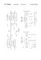
- FIG. 1is an illustration of a cross-connect apparatus which is typically employed by an information service provider for terminating, cross-connecting, and accessing a number of communication lines;
- FIG. 2is a illustration of a cross-connect apparatus which is typically used when cross-connecting a variety of digital communications equipment;
- FIG. 3is a depiction of an intelligent cross-connect system which operates in accordance with the principles of the present invention
- FIG. 4is a perspective view of a cross-connect shelf within which a number of cross-connect circuits and a shelf controller are installed;
- FIG. 5illustrates an embodiment of a scanning bus topology and system architecture which is used to communicate scanning signal information in accordance with a scanning methodology of the present invention
- FIG. 6is an illustration of a pair of cross-connect circuits which communicate information signal information there between over a standard multi-conductor connection, and further communicate scanning signal information over a trace connection;
- FIG. 7is a front view illustration of the circuit shown in FIG. 6 which includes a number of jacks, LEDs, and wire-wrap pins;
- FIG. 8is schematic illustration of one embodiment of the circuit shown in FIG. 6;
- FIG. 9is an illustration of a standard bantam plug over which scanning signal information is communicated by use of the shielding sleeve conductor of the bantam plug;
- FIG. 10is an illustration of a cross-connect shelf which includes a shelf controller that communicates with a pair of connected cross-connect circuits to effectuate a scanning procedure utilizing the trace connection in accordance with the principles of the present invention
- FIG. 11is a system level illustration of a scanning apparatus in which cross-connect circuit identification information is acquired by a shelf controller and communicated to a main computer for storage in a cross-connect database;
- FIG. 12illustrates an embodiment of a shelf controller which communicates a scanning signal through the shielding sleeve of a patch cord connecting a pair of connected cross-connect circuits for the purpose of determining the identity of the connected circuits;
- FIG. 13is a system block diagram depicting the various components constituting one embodiment of a shelf controller
- FIGS. 14-15illustrate in flow diagram form various process steps associated with the control of single or multiple TRACE LEDs in accordance with an embodiment of a scanning methodology of the present invention
- FIG. 16Aillustrates one embodiment of a shelf controller circuit which includes a number of receive and transmit registers associated with each of a number of cross-connect circuits with which the shelf controller communicates;
- FIG. 16Billustrates in greater detail various receive and transmit registers and corresponding receiver and transmitter devices, in addition to other components, which are embodied in, and communicate with, the shelf controller circuit embodiment shown in FIG. 16A;
- FIG. 16Cillustrates a portion of the shelf controller shown generally in FIGS. 16A-16B embodied in one or more ASICS;
- FIGS. 17-19illustrate in flow diagram form various process steps associated with a scanning methodology in accordance with a first embodiment of the invention
- FIG. 20is an illustration of transmit and receive registers and a collision detection circuit associated with a pair of cross-connected circuits which are used to facilitate the implementation of the scanning methodology depicted in FIGS. 17-19;
- FIGS. 21A-21Billustrate state tables associated with the respective circuits A and B illustrated in FIG. 20, the tables depicting the state of the transmit and receive registers and the efficacy of collision detection during implementation of the scanning methodology depicted in FIGS. 17-19;
- FIG. 22is a schematic illustration of one embodiment of the collision detection circuit shown in FIG. 20;
- FIGS. 23A-23Cillustrate timing diagrams associated with the operation of the collision detection circuit shown in FIG. 22;
- FIGS. 24-25depict in flow diagram form various process steps associated with a scanning methodology in accordance with a second embodiment of the present invention.
- FIG. 26illustrates various process steps associated with a scanning methodology in accordance with a third embodiment of the invention.
- FIGS. 27-28respectively illustrate a lost connection and new connection monitoring procedure in accordance with one embodiment of the present invention.
- FIGS. 29-36illustrate various information screens which are displayable to a user of the intelligent cross-connect system through use of a graphical user interface which cooperatively operates with a cross-connect database.
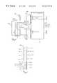
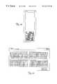
- FIG. 1there is provided a generalized depiction of a cross-connect apparatus which provides a situs for terminating, cross-connecting, and accessing a number of transmission lines capable of communicating signals of varying types.
- a number of the cross-connect apparatuses of the type shown in FIG. 1are typically installed in equipment frames or bays and interconnected as part of a telephony network.
- the cross-connect baysserve as a centralized hubs for interconnecting various types of equipment which may communicate information at various data rates.
- a digital trunk 36includes a number of signal lines 38 associated with a first communications equipment facility, each of the signal lines 38 being terminated or otherwise coupled to a respective cross-connect circuit 44 installed in a patch panel or shelf 40 .
- a second digital trunk 46 operated by a second communications equipment facilityincludes a number of signal lines 48 which are terminated on respective cross-connect circuits 54 mounted in a second patch panel or shelf 50 .
- Individual circuits 44 of shelf 40are typically “cross-connected” to respective circuits 54 of shelf 50 through use of either hard-wired connections or temporary patch connections established therebetween.
- a digital signal transmitted through signal line 38 a of the digital trunk 36is cross-connected to signal line 48 a of the digital trunk 46 over cross-connected circuits 44 a and 54 a respectively mounted in patch shelves 40 and 50 .
- circuits 44 a, 54 a of patch shelves 40 , 50are connected via a hard-wired connection 56 in the depiction provided in FIG. 1, but may alternatively be established through use of a temporary patch connection, such as patch connection 58 connecting circuits 44 b and 54 b.
- a cross-connect tracking system and methodology in accordance with the principles of the present inventionfully addresses the complex problem of identifying all interconnected cross-connect circuits established through a central office, and further identifies whether such interconnections are established over a hard-wired or temporary patch connection. Any modifications made to existing circuit connections are detected in near real-time whether such modifications are established over hard-wired or patch connections.
- various types of information concerning each connection established within the central officeis maintained in a database which is updated in near real-time so as to reflect the current state of all connections.
- a graphical user interfacecooperates with the database, typically under user control, and provides a user the ability to access connection records of interest, to visually display simulated depictions of selected connections, and to generate a variety of reports derived from the connection information maintained in the database.
- the graphical user interfacemay also be used to guide a technician through a maze of connections to specific circuit locations which may require repair or redirection through use of a patch cord.
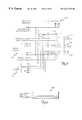
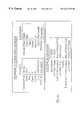
- FIG. 2illustrates an exemplary configuration of a digital cross-connect (DSX) system of a type suitable for employment in an intelligent cross-connect system of the present invention.
- the cross-connect system shown in FIG. 2is typically used as an interconnection point between outside plant facilities and telecommunications equipment for accommodating high-speed digital connections having data rates on the order of 1 Mbps to 50 Mbps.
- a typical digital cross-connect systemcontains only passive connections which are extremely reliable, such that no active electronics interfere with the information signals passing through the cross-connect system.
- stringent reliability requirements established by information service providersseverely limit and typically preclude the use of active electronics within the information signal circuit path, which significantly increases the difficulty of effectively and efficiently determining the identity of all connections established within a cross-connect system.
- the cross-connect system shown in FIG. 2provides a termination point for permanently connected equipment, and also accommodates a series of connection jacks, termed bantam jacks in the industry, whereby patch cords may be employed to temporarily redirect connections.
- a service provideris able to manually patch around trouble spots, or rearrange equipment and facilities without service interruption.
- the particular embodiment shown in FIG. 2illustrates a DSX- 1 system designed to terminate DS 1 (1.544 Mbps) circuits, and also accommodates other data rates such as E 1 (2.048 Mbps) or DS 3 signals (44.736 Mbps) associated with DSX- 3 systems.
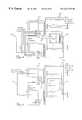
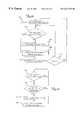
- FIG. 3there is illustrated an embodiment of a cross-connect system which operates in accordance with the principles of the present invention.
- a central office 60is typically organized in a hierarchical fashion, and includes a number of bays or frames 66 , each of which houses several shelves 72 of cross-connect circuits 74 .
- a specified number of individual cross-connect circuits 74are removably installed in each of the shelves 72 .
- a shelf controller 76also removably housed in each of the shelves 72 , communicates with each of the cross-connect circuits 74 installed within the shelf 72 .
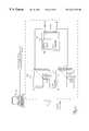
- FIG. 4An embodiment of a shelf 72 within which a number of individual cross-connect circuits 74 and a shelf controller 76 are removably installed is illustrated in FIG. 4.
- a number of individual cross-connect circuits 74may also be grouped to form packs 73 of circuits 74 , such as four circuits 74 being grouped to form a modular “quad” card 73 .
- the shelf 72includes a printed circuit board (PCB) backplane which provides for the communication of information and power signals between the circuits 74 and controller 76 , and provides connectivity with other circuits 74 , shelf controllers 76 , and components of the cross-connect system 60 .
- PCBprinted circuit board
- Each of the shelf controllers 76communicates with a bay controller 64 which, in turn, communicates with a main computer 62 , such as a central office computer.
- the bay controller 64cooperates with the main computer 62 to coordinate the activities of the shelf controllers 76 installed in one or more of the bays 66 .
- a bay controller 64may, for example, service up to 32 bays 66 of cross-connect equipment.
- each shelf controller 76may communicate directly with the main computer 62 .
- the main computer 62may be employed as a central information and control resource for a number of bay controllers 64 maintained at a central office 60 . It is understood that the bays 66 of cross-connect equipment constituting a central office may be situated at a single location, such as a building, or distributed at a number of geographically separated locations.
- Connection informationis acquired from individual shelf controllers 76 and communicated to the main computer 62 , where it is stored in a cross-connect database 65 .
- a graphical user interface (GUI) 63is employed by a user to access the database 65 .
- GUIgraphical user interface
- the main computer 62may constitute a single computer platform or a distributed platform connected via a network or other communications infrastructure.
- the database 65may constitute a single non-volatile memory device or a distributed memory device.
- a cross-connect system operating in accordance with the principles of the present inventionadvantageously exploits TRACE wire connections as a communications conduit for implementing various connection sensing, identification, and monitoring functions. It is understood in the industry that TRACE wire or lamp wire is used in a conventional DSX system to connect the TRACE LEDs of each of the cross-connected circuits for purposes of manually tracing a connection.
- the cross-connect system of the present inventionutilizes TRACE wire and patch cord connections to effectively form scanning busses over which scanning signals are transmitted in accordance with a unique scanning methodology.
- scanning busrefers to either one or both of TRACE wire and patch cord connections.
- a scanning busis intended to refer to any connection, whether electrical, optical or otherwise, within a cross-connect system other than a connection intended to be used exclusively for communicating information signals.
- a scanning bus or networkis illustrated which is used to communicate connection and other information between cross-connect circuits, shelf controllers, and a main computer of the intelligent cross-connect system.
- the scanning busincludes a network connection 86 over which shelf controllers 76 of a particular bay or bays 66 communicate with each other.
- the network connection 86may constitute an EIA-485 serial communication connection, which is understood to be a four-conductor, multi-drop, full-duplex balanced signal serial bus connection.
- a central office of a telecommunications service providerincludes one-hundred bays 66 of cross-connect equipment.
- Each bay 66includes thirteen shelves 72 , with each shelf 72 housing eighty-four individual cross-connect circuits 74 .
- the shelf controllers 76 installed in respective shelves 72 of each bay 66communicate with a bay controller 64 and with a main 62 over a private ethernet connection 92 .
- each bay controller 64may be viewed as constituting a node of the central office scanning network.
- the central office or main computer 62accumulates connection information acquired by each of the shelf controllers 76 to develop cross-connection records for the entire central office.
- Each of the bay controllers 64cooperates with their respective shelf controllers 76 to determine all hard-wired and patch connections established at the central office, to detect changes to the various connections, and to update a cross-connect database 65 accessed by the main computer 62 on a near real-time basis, such that any connection changes are automatically reflected in the continuously updated database.
- a service provideris able to query and display cross-connect records 65 for any circuit within the system.
- a hard-wired connectionmay be established between a pair of circuits housed within the same bay, such as circuits 3 and 2 of shelves 12 and 2 , respectively, of bay 1 , or between circuits housed within the same bay and shelf.
- a hard-wired connection 98respectively may also be established between circuits housed in different bays, such as between circuit 3 of shelf 1 , bay 1 , and circuit 84 of shelf 13 , bay 99 .
- patch cord connectionsmay be established between circuit pairs of a common bay or of different bays, such as between circuits 84 of shelf 1 for bays 1 and 2 , respectively.
- a bridging repeater 98may be employed within the scanning bus configuration for effecting scanning operations between cross-connect circuits of distantly located bays.
- a bay controller 64is embodied as a single board computer or PC motherboard running an appropriate communications protocol to effect transmission between the private ethernet 92 and the shelf controllers 76 .
- the ethernet protocolmay be an ASN.1 compliant simple network management protocol (SNMP) running on top of TCP/IP. Data rates ranging between approximately 10 Mbps and 100 Mbps are obtainable using this arrangement.
- a bay controller 64communicates with a number of shelf controllers 76 using an EIA-485 bus protocol, in which the bay controller 64 operates as a single master which polls the shelf controllers 76 .
- the shelf controllers 76transmit information only when polled by the bay controller 64 .
- each shelf 72is assigned a unique 48 bit ID number.
- the bay controller 64retrieves the 48 bit ID of all shelves 72 connected thereto. The bay controller 64 then assigns each shelf an 11 bit ID number which will be used in subsequent communications.
- Arbitration on the EIA-485 connectionis facilitated by operating in a four wire, full-duplex mode; two for transmit, and two for receive. If there is more than one new device on a particular EIA-485 bus, as may occur at initial power-up, an arbitration scheme using the 48-bit shelf ID is employed to resolve collisions. It is noted that in an embodiment of a shelf controller that utilizes a universal asynchronous receiver/transmitter (UART), the UART is byte oriented and generally must complete the current byte transmission before reacting to a collision.
- UARTuniversal asynchronous receiver/transmitter
- each nodeWhen a collision on an EIA-485 connection occurs, each node initially uses the least significant bit of the shelf ID to resolve the collision. When a new device poll event occurs and bus inactivity has been verified, each node attempts to respond to the new device poll. If a collision occurs, the nodes stop transmitting. If the shelf ID bit of a node implicated in the collision is zero, this node responds again immediately. The next most significant bit of the shelf ID for this node is then pointed to for arbitrating subsequent collisions. Otherwise, the node awaits the next new device poll event.
- MIBManagement Information Base
- the MIBis an industry standard data format which provides for the network management of a device. Within its device-specific structure, the MIB data contains all of the information about the bay controller 64 and all of the associated shelf controllers 76 and alarm collection shelves, as well as any future devices that are connected to it.
- a request from the bay controller 64typically indicates the element of the MIB data of interest, and the response is generally the same message with appropriate value(s) added.
- the bay controller 64initiates an SNMP trap.
- the main computer 62then responds in an appropriate manner so that the bay controller 64 is informed that the message was received.
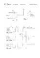
- each cross-connect circuit 102 , 104plugs into a shelf or chassis 100 .
- Permanent equipment connectionsare terminated on the rear of the shelf 100 .
- the permanent connections established on the rear of the shelf 100are effectively passed through the cross-connect circuits 102 , 104 to the front of the circuits 102 , 104 .
- Each piece of equipmentmay be cross-connected to other equipment components typically by installing a five-conductor jumper cable to terminals extending from the front of circuits 102 , 104 .
- the five-conductor cableis an industry standard cable that is used by a variety of cross-connect equipment suppliers.
- the five conductorssupport a transmit and receive pair, plus an additional TRACE conductor.
- this five-conductor cableconstitutes a twisted pair cable that is “wire-wrapped” to appropriate terminal posts provided on the circuits 102 , 104 .
- cross-connectionsare established using two coaxial jumpers for transmit and receive, along with a third jumper that connects the TRACE line contacts.
- a separate electrical conductoris typically used as the TRACE conductor.
- connection information in the form of optical signalsmay be communicated along a separate fiber optic TRACE connection.
- the TRACE or “TL” connectionprovides a means of manually tracing the connection between cross-connected circuits, such as circuits 102 , 104 shown in FIG. 6 .
- the TRACE lineis grounded, which causes TRACE LEDs 106 of the respective circuits 102 , 104 to illuminate. Illumination of the TRACE LEDs 106 of a cross-connected circuit pair permits manual tracing of the circuits and identification of the cross-connected circuit locations within the central office.
- FIG. 7is a front view depiction of the circuits 102 , 104 shown in FIG. 6, and illustrates an embodiment in which a singe TRACE LED 106 is employed.
- the cross-connect circuit embodied in the schematic illustration of FIG. 8includes two TRACE LEDs 106 , namely, a red and a green LED 106 .
- the front panel of a cross-connect circuitmay additionally include a two digit, seven segment display with incrementing momentary pushbuttons for the two digits and a clear momentary pushbutton, all of which is controlled with firmware.
- firmwareresiding in a memory provided in a cross-connect circuit, shelf controller, or bay controller may be installed and updated by implementing an appropriate firmware downloading procedure.
- a telecommunications service providermay manage over one hundred bays of cross-connect equipment maintained at a single location, with many such installations established in various cities.
- a single central office locationwhich houses one hundred bays containing thirteen shelves within which eighty-four cross-connect circuits are installed provides for a total of 109,200 connections established at this single location.
- the cross-connect monitoring system of the present inventionprovides for accurate and continuous electronic monitoring and updating of connection records for any number of connections.
- FIG. 8is a schematic representation of the MONITOR, OUTPUT, and INPUT bantam jacks 108 , 110 , 112 and ancillary circuits shown in FIG. 7.
- a partial showing of a typical bantam plug 120which is connected to each of the opposing ends of a patch cord, is shown in FIG. 9 .
- the normal function of a patch cord when used within a cross-connect systemis to temporarily re-direct a circuit connection to a termination point different from that established by the circuit's hard-wired connection.
- a conventional bantam plug 120 used in the industry for establishing patch connectionstypically includes three conductors which are identified in telephony terms as TIP, RING, and SLEEVE (i.e. SHIELD).
- the TIP and RING conductorsare used to transmit information signals, while the SLEEVE or SHIELD is used as an interference protection mechanism (e.g., ground shield).
- an interference protection mechanisme.g., ground shield.
- FIG. 8when a bantam plug 120 is inserted into either the OUT or IN jack 110 , 112 , the respective OUT or IN signal will redirected over the patch cord, and the connection to the TN/RN wired cross-connect 122 will be broken.
- the TL, TR, and RN signal contacts 122represent hard-wired (e.g., wire-wrapped) connections, and the IN/OUT R, T connections 124 represent the rear permanent connections.
- FIGS. 10-12there is depicted an embodiment of various circuit elements which are used in an intelligent digital cross-connect system to electronically and automatically identify and monitor all connections established through the circuits of the cross-connect system on a continuous basis.
- the TRACE wire conductor 133is utilized in an unconventional manner, in that a scanning signal is communicated through the TRACE wire conductor 133 in accordance with a unique cross-connect scanning methodology.
- a shelf controller 136generates a scanning signal, which includes location identification information associated with a transmitting cross-connect circuit 132 , and transmits the scanning signal across the TRACE wire conductor 133 of the transmitting circuit 132 .
- the scanning signal communicated by the transmitting cross-connect circuit 132is received by a receiving cross-connect circuit 134 .
- the shelf controller 136 associated with the receiving circuit 134reports the transmitting and receiving circuit location identification information to a main computer, such as the bay controller 64 or main computer 62 shown in FIG. 3 .
- the receiving circuit 134may be located in the same shelf 130 as the transmitting circuit 132 , a different shelf 130 within the same bay, or a shelf of a bay distantly located from that housing the transmitting circuit 132 .
- the shelf controller 136dedicates an individual connection for each TRACE connection of individual cross-connect circuits installed in a particular shelf 130 .
- Each shelf controller 136transmits circuit location identification information, typically by use of a digital scanning signal, across each of its TRACE wire connections either in a particular sequence or in parallel depending on the particular scanning algorithm employed.
- the shelf controllers 136 of a cross-connect systemcollectively identify the location of all circuits established through the cross-connect system. Unused circuits are also identified. All shelf controllers 136 in all equipment bays proceed through this general scanning operation in order to identify all of their respective connections.
- Each shelf controller 136will then report its connection information to a main computer 64 via a data connection.
- a patch cord 143may be employed to temporarily re-direct information signals between cross-connect circuits other than those connected through use of a hard-wired connection.
- a scanning signal produced by the shelf controller 136is transmitted over the SLEEVE or SHIELD conductor of the patch cord 143 to a newly selected receiving cross-select circuit 134 .
- Information identifying the location of the transmitting circuit 132is encoded in the scanning signal and used together with information identifying the selected receiving circuit 134 to identify the newly established patch connection. This information is similarly communicated to a central computer.
- SLEEVE or SHIELD conductor of the patch cord 143advantageously provides a conduit for communicating scanning signal information without requiring additional patch cord conductors. It is understood that modifying the configuration of an industry standard patch cable so as to include an additional conductor would result in increased costs and the potential of making obsolete hundreds of thousands of cross-connect patch cables currently in use. Because the transmission speed of the scanning data is relatively low, no appreciable interference problems arise with the use of the shield conductor of the patch cord 143 .
- FIG. 13A generalized system block diagram of a shelf controller 150 is depicted in FIG. 13 .
- the shelf controller 150includes a micro-controller 152 , which communicates with a memory 154 and various digital devices 158 , 160 , 162 over a data bus 164 .
- the general function of the digital interface circuits 158 , 160 , 162is to receive or transmit data from a large number of input/output sources and, when requested, present this data to the micro-controller's data bus 164 .
- the micro-controller 152then stores all of the connection and status information into the memory 154 , and when requested, transmits this information over the serial data bus 168 to the main computer.
- the micro-controller 152communicates with an ancillary processor, such as a bay controller 64 , through serial data transceiver circuits 156 .
- an ancillary processorsuch as a bay controller 64
- a digital interface circuit 158which is coupled to a number of jack sense lines, receives signals indicating the presence or absence of a bantam plug in any one of the MONITOR jack 108 , the OUTPUT jack 110 , or the INPUT jack 112 .
- a digital interface device 162communicates with a TRACE LED 106 and controls the illumination, flashing, color selection, and other operations of the TRACE LED 106 .
- the shelf controller 150may activate the TRACE LEDs 106 for a pair of connected circuits so as to simulate a “trace” as would otherwise occur within a conventional cross-connect systems.
- the scanning signal transmitted through a TRACE connection or patch connectionprovides location identification and status information regarding the transmitting cross-connect circuit.
- Table 1there is provided various types of information that may be encoded in a scanning signal in accordance with one embodiment of the present invention.
- the identification of the shelf number and cross-connect circuit numberare encoded using eleven and seven bits, respectively, irrespective of whether the scanning signal is transmitted over a TRACE wire connection or patch connection.
- the Path Number fieldindicates the transmission path as being either the TRACE, Patch IN, or Patch OUT connection. It is to be understood that the scanning signal fields provided in Table 1 represents a non-exhaustive list of information variables which may be encoded in a scanning signal. Other information different from or in addition to that included in Table 1 may also be encoded in the scanning signal.
- Each of the shelf controllersmaintains a local database of identification and status information concerning the cross-connect circuits with which it communicates.
- Table 2below provides an example of various types of information which may be maintained and updated in the local database of a shelf controller.
- the four LED bitsprovide for four LED states, including OFF for both Red and Green LEDs. Combining these states provides the opportunity to use yellow or orange, depending on the current limiting resistors chosen.
- the LEDsmay change state every eighth of a second allowing for a variety of LED presentations to be implemented.
- the scanning signals which are received by a receiving cross-connect circuitare communicated to a main computer and preferably stored in a database containing cross-connect information.
- a database containing cross-connect informationAn exemplary set of database fields for such a database is provided below in Table 3.
- the cross-connect databaseprovides for the storage and access of a comprehensive set of information concerning each and every cross-connection established through a central office.
- the databaseincludes fields generally corresponding to those associated with the information provided in Tables 1 and 2 above, as well as other information of interest, such as the central office location, name, floor, and location of a particular bay, connection history, and user or administrator comments, for example.
- Circuit TypeIdentifies whether Circuit Port is a “Facility Side”, or “Network Side” Port Circuit Free-Format Description Field for the Description
- Customer ConnectionIdentifies whether the Port is Connected Status or not Connected Connection Provides a History of Connection Status History Information - Including Time/Date Stamp, Circuits Connections and Disconnections Comments Free-Format Comment Field with USER ID, Date/Time Stamp Cross-Connect Fields of Detailed Connection Information Information
- One of several functions performed by the shelf controller 150involves detecting a change in the condition of a patch cord, such as whether any patch cords have been installed into or removed from a particular jack of a particular cross-connect circuit.
- additional electrical contacts within each of the MONITOR, OUTPUT, and INPUT jacks 108 , 110 , 112provide an indication to the shelf controller 150 as to the status of these jacks (i.e., bantam plug present or absent). All of the jack sense lines are connected via the backplane of a shelf chassis to the shelf controller 150 .
- the micro-controller 152periodically polls the status of each of the bantam jacks, stores the status information in the memory 154 , and reports this information to the main computer when requested.
- the shelf controllerwhen the main computer issues a command instructing a selected shelf controller to activate the TRACE LED of a particular circuit, the shelf controller causes the appropriate circuit LED to illuminate according to a pre-established flash pattern.
- a flash patternrefers to a LED flash program that indicates various LED illumination parameters, such as steady and/or flash durations, flash speed, single or multiple colors usage, and other LED operating parameters.
- the TRACE LEDwill typically remain illuminated until the shelf controller receives an instruction from the main computer to turn off the TRACE LED or until such time as a flash pattern timer expires.
- the main computermay also initiate a command instructing a selected shelf controller to cause the TRACE LED of a particular circuit to flash.
- the shelf controllermay store FLASH-ON and FLASH-OFF timing information, and will typically cause a TRACE LED to continue flashing at a specified rate until it is requested to terminate the flashing operation.
- TRACE LED control and jack sense proceduresOne particular function that is implemented through execution of the TRACE LED control and jack sense procedures, as mentioned previously, is the simulation of an industry-standard “trace” operation. Such an operation typically involves placing a bantam plug into the MONITOR jack of a particular circuit to initiate the trace. In a standard digital cross-connect system, this would result in grounding of the TRACE wire, thereby causing the TRACE LEDs at both ends of the circuit connection to illuminate.
- insertion of the bantam plug in the MONITOR jackis sensed by the shelf controller 150 which, in response, transmits an LED flash command over the scanning bus.
- the LED flash commandis decoded by the shelf controller associated with the receiving partner circuit which causes the LED(s) of the partner circuit to illuminate in accordance with a selected flash pattern.
- the shelf controllerinitiates 200 a TRACE simulation procedure by selecting 202 a first circuit installed within the shelf. If an LED flash command issued by the main computer has been previously transmitted 204 with respect to the selected circuit, the shelf controller detects this activity and selects 206 another cross-connect circuit in the shelf. If an LED flash command has not been issued, the shelf controller senses 212 the MONITOR jack of the selected circuit.
- the flash pattern function for the selected cross-connect circuitis initiated 218 and the flash pattern timer is turned on. If the MONITOR jack is occupied 212 and the flash pattern is already active 216 , the TRACE LED 106 for the selected circuit is set 222 to a steady ON state if the flash pattern timer has expired 220 . If the flash pattern timer has not expired 220 , the shelf controller selects 206 another cross-connect circuit of the shelf.
- the flash pattern operationis halted, and the shelf controller selects 206 another cross-connect circuit of the shelf.
- the TRACE simulation procedurecontinues until all of the cross-connect circuits of the shelf have been monitored 208 , 210 .
- the shelf controllersenses 230 the status of the MONITOR jack of all circuits with which it communicates. This monitoring process continues until such time as a FLASH command is received 232 from the main computer. If the command received 238 from the main computer is not a CLEAR LED instruction, then the shelf controller initiates 242 an LED flash procedure for the indicated cross-connect circuits with the indicated illumination pattern.
- the flash patternis overridden 244 under this condition. If the flash command received 232 from the main computer is a CLEAR LED instruction 238 , and if the locate flash pattern function is in a flash or steady on state 236 , the LED flash is cleared and the flash pattern function is restored for the indicated cross-connect circuit. If the locate function is not in a flash or steady on state 236 , then the LED is turned off 234 .
- the cooperative operation between the shelf controller and the main computerprovides the opportunity to effect a full range of control over the TRACE LEDs for a variety of purposes. It is noted that one or more LEDs of a cross-connect circuit may be controlled by the shelf controller, and that the LEDs may be monochromatic or multi-chromatic in type. By way of example, cooperation between the shelf controller and main computer provides the ability to effectively guide a technician through various patch connection or disconnection operations.
- a “patch pending” fileis created which indicates various connections or disconnections to be effected by a technician to accomplish a particular objective.
- the patch pending filewhen executed by the main computer, may control multi-colored TRACE LEDs of specified circuits as a means of visually directing the work of a technician when establishing and breaking cross-connections.
- a flashing green LED indicationfor example, may identify circuits in which a patch cord is to be inserted, while a flashing red LED indication may identify circuits in which an existing patch cord is to be removed.
- a patch pending filetypically contains information identifying the specific sequence by which patch cord installation or removal is to be accomplished by a technician.
- the main computerthen steps a technician through each change, one circuit pair at a time. Since the main computer knows precisely when and where a patch cord is to be inserted or removed, the implicated LEDs may continue to flash until the technician effects a proper connection or disconnection for a particular circuit.
- a patch pending filemay be created which provides information concerning contingent or back-up connections that may be established in the event of a network outage.
- a patch pending filemay identify important circuits which require immediate restoration during temporary or extended outages.
- technicianstypically use a shot-gun approach when attempting to identify all cross-connected circuits effected by the outage and the location of temporary patches that must be effected in order to restore important circuit connections.
- Creation of a patch pending file well in advance of an outage situationprovides an opportunity for the service provider to develop a well-considered strategy for dealing with any number of potential outage scenarios.
- an appropriate patch pending filemay be selected and executed to implement an efficient, coordinated patching procedure for restoring key circuits. On-site technicians may then quickly proceed through the cross-connect system guided by the LED patch sequencing process in their effort to patch and unpatch specified circuit connections. It can be appreciated that use of patch pending files in this manner saves precious time in restoring important and other circuits impacted by an outage, which would otherwise be wasted on looking up records and sorting out needed connection information under stressful conditions associated with a major outage.
- FIGS. 16A-27there is depicted various embodiments of a scanning methodology and apparatus by which all connections established through a cross-connect system or central office may be identified, and status information acquired and updated for all connections on a continuous basis.
- the circuit 600 depicted in FIG. 16 AThe circuit 600 is typically incorporated as part of the shelf controller and may be embodied in a micro-controller, an Application Specific Integrated Circuit (ASIC) or Field Programmable Gate Array (FPGA), for example.
- ASICApplication Specific Integrated Circuit
- FPGAField Programmable Gate Array
- the circuit 600includes a number of receive registers 602 and transmit registers 604 associated with each cross-connect circuit coupled to the shelf controller.
- the circuit 600will include 84 receive register sets 608 and 84 transmit register sets 618 , one receiver and transmit register set 608 , 618 being respectively associated with each of the 84 cross-connect circuits.
- each receive and transmit register set 608 , 618respectively includes a TRACE register 610 , 620 , a Patch IN register 612 , 622 , and a Patch OUT register 614 , 624 .
- each of the TRACE, Patch IN, and Patch OUT registersconstitutes a First-In-First-out (FIFO) register or stack, it being understood that other buffering or memory implementations may be employed.
- FIFOFirst-In-First-out
- the TRACE, Patch IN, and Patch OUT FIFOs 610 , 612 , 614 associated with the receive register 602may each be coupled to a respective receiver circuit (not shown), and the TRACE, Patch IN, and Patch OUT FIFOs 620 , 622 , 624 associated with the transmit register 604 may each be coupled to a respective transmitter circuit (not shown).
- each cross-connect circuitis thus provided with three transmitters and three receivers.
- datamay be transmitted from and receive by the three dedicated receive and transmit FIFO sets in a simultaneous or parallel manner.
- FIG. 16Bis generally illustrative of this particular embodiment.
- a single receivermay be multiplexed across the TRACE, Patch IN, and Patch OUT FIFOs 610 , 612 , 614 associated with each cross-connect circuit
- a single transmittermay be multiplexed across the TRACE, Patch IN, and Patch OUT FIFOs 620 , 622 , 624 .
- Another alternative configurationincludes a single multiplexed transmitter and three dedicated receivers. It is appreciated that use of a multiplexed receiver or transmitter requires some form of sequential or selective circuit path switching amongst the associated receive or transmit FIFOs.
- a single ASICprovides all of the logic required to support 16 cross-connect circuits.
- the number of cross-connect circuits supported in a particular shelf configurationmay be expanded simply be installing additional ASICs.
- Each sub-circuit of an ASICsuch as Circuit # 1 or Circuit #N shown in FIG. 16A, includes three physical pins respectively dedicated to the three circuit paths (i.e., TRACE, Patch IN, Patch OUT). Internally, the receive and transmit logic for each pin is functionally OR tied.
- the ASICincludes three transmitters and three receivers for each sub-circuit so as to provide for simultaneous data transmission and reception.
- the pins of the ASIC coupled to each cross-connect circuitinclude the following: TRACE Bus; Patch IN Bus; Patch OUT Bus; MONITOR Jack Occupied; IN Jack Occupied; OUT Jack Occupied; Red LED; Green LED; and Circuit Pack Present pins. It is noted that a Circuit Pack Present signal received at the Circuit Pack Present pin indicates the presence of particular grouping or pack of cross-connect circuits within the shelf.
- the ASICalso includes a number of standard pins, such as data bus, address bus, CLK, and other control signal pins.
- a central processing unit (CPU) or micro-controller of the shelf controllercooperates with the circuit 600 to coordinate the operation of the receive and transmit register 602 , 604 .
- the receive and transmit FIFOs 602 , 604 of a particular cross-connect circuitare employed to store data pertaining to the connection established between the particular circuit and the circuit connected thereto, and to effect the various scanning procedures implemented in accordance with the principles of the present invention.
- each cross-connect circuittransmits its unique identification (ID) information or code to a partner circuit connected thereto.
- IDunique identification
- the partner circuit receiving the transmitting circuit's ID codestores this data and, when requested by the bay controller or main computer, transmits the transmitting circuit ID code and its own ID code to the main computer.
- Other connection status informationmay also be communicated between the transmitting and receiving circuits and transmitted to the main computer.
- the receiving circuitsneed transmit their respective connection information to the main computer in order to obtain the identification of all cross-connected circuit pairs within the system. It is important to note that the transmitting side generally does not know of the status of the receiving side. A transmitting circuit, therefore, will continue to transmit at regular intervals, thus providing a keep-alive signal to the receiving partner circuit. Moreover, after acquiring an initial set of connection information from all receiving circuits, only those receiving circuits containing new connection or disconnection information need pass the information to the bay controller or main computer.
- all circuit connectionswill be scanned and identified within the time it takes to transmit a single cross-connect circuit ID bit string, irrespective of the size of the cross-connect system (i.e., number of cross-connect circuits). If, for example, it is assumed that a given scanning methodology employs a circuit ID code of n bits in length, that start/stop and stuff bits constitute m bits, and that the clock speed is given as CLK Hertz, then the total scan time required to identify all circuit connections is given by:
- the time required to identify all cross-connected circuits using the scanning approach depicted in FIGS. 17-23Cis relatively short and constant (e.g., 100-500 milliseconds), regardless of whether the system contains ten thousand, one-hundred thousand, or even a million cross-connected circuits.
- the circuit 600 depicted in FIG. 16Arepresents one conceptual embodiment of a Transmit Table, it being understood that other implementation may be employed in hardware and software to facilitate the scanning methodology.
- the Transmit Tableis established in which circuit ID and patch status information is loaded for each of the circuits coupled to a respective shelf controller of the cross-connect system.
- the loading functionsuch as that depicted in FIGS. 17-18, takes into consideration all hard-wired connections between circuit pairs, and, importantly, all patch connections established using patch cords connected to the IN/OUT jacks of the circuits. As such, all physical cross-connections, whether hard-wired or patch connections, are identified.
- a typical Transmit Table loading operationis initiated upon receiving 300 a broadcast command issued from the main computer.
- each of the transmit TRACE FIFOs 620 of each cross-connect circuit within a shelfis loaded with a TRACE identification code (TRACE ID).
- TRACE IDrepresents a code which uniquely identifies the TRACE jack of a particular cross-connect circuit.
- Patch IN and Patch OUT IDsrepresent codes which uniquely identify the Patch IN and Patch OUT jacks of a particular cross-connect circuit.
- the loading procedure illustrated in FIGS. 17-18is implemented by each shelf controller for all bays of cross-connect equipment in a contemporaneous, parallel manner.
- the shelf controllerscans 304 each of the circuit receive register 602 to determine 306 if a circuit ID currently resides in the circuit's receive TRACE FIFO 610 . If a valid circuit ID is stored in the receiver TRACE FIFO 610 for a particular circuit, the ID of the partner circuit has been previously received. As such, the identity of the cross-connected circuits is already known, and the scanning operation need not be repeated 308 for this circuit connection. Although not required, it may be desirable to perform a re-scan operation for the particular circuit connection.
- the shelf controllerdetermines whether a patch cord has been inserted into either of the Patch IN or Patch OUT jacks. In particular, if a circuit ID is not currently residing 310 in the receive Patch IN FIFO 612 for the selected circuit, the shelf controller determines 312 whether the Patch IN jack is occupied, and if so, adds 314 the Patch IN ID to the transmit patch IN FIFO 622 of the Transmit Table for the selected circuit.
- the shelf controlleradds 320 the Patch OUT ID to the transmit patch OUT FIFO 624 of the Transmit Table for the selected circuit. All circuits coupled to the shelf controller are similarly processed 322 . After processing all of the respective circuits associated with the shelf controller, the scanning procedure generally depicted in FIG. 19 is initiated 324 . The shelf controller reports 326 completion of the scanning procedure 324 to the main computer upon completion.
- all circuits within the cross-connect systemtransmit their respective full circuit ID codes according to the procedure illustrated in FIG. 19 .
- all shelf controllerstransmit ID and other information for those circuits having circuit ID codes currently loaded in the Transmit Table. These transmissions can take place over several circuit paths simultaneously, such as over the TRACE conductor or the Patch IN and OUT conductors.
- a “listen before transmitting” approachis employed during the scanning operation in an attempt to minimize collisions and transmissions across the scanning bus. If a transmission is detected on a connection coupled to a particular circuit identified in the Transmit Table, the transmitting circuit is prevented from making further transmissions and its ID is removed from the appropriate transmit FIFO 618 of the Transmit Table. In this situation, the incoming transmission is typically, if not exclusively, a circuit ID being communicated from a partner (i.e., cross-connected) circuit.
- a collision arbitration procedureis initiated whereby one of the two transmitting circuits (identified as a “transmitter”) is permitted to continue transmitting its full ID, and the other circuit is instructed to cease its transmission.
- This circuit's IDis removed from the Transmit Table, and the circuit is identified as a “receiver” for subsequent transmissions, although it may be desirable to reset all circuits to “transmitters” and repeat the collision arbitration procedure for each subsequent transmission.
- any change in hard-wired or patch connectivity with respect to a particular circuitregardless of whether the circuit is identified as a transmitter or receiver, is detected by the shelf controller.
- the new connectionwill be scanned in the same manner as those associated with circuits previously loaded in the Transmit Table.
- the implicated circuitslose their respective “transmitter” or “receiver” identifications.
- any modification to an existing connection or addition of a new connectionwill be detected and identified within a subsequent single scanning period (i.e., the time it takes to transmit a single cross-connect circuit ID bit string).
- FIG. 20is an illustration of two cross-connected circuits each including respective transmit (XMIT) and receive (RCV) FIFOs 381 , 389 and 383 , 391 coupled to respective collision detection circuits 385 , 387 .
- the pair of circuits A and Bare connected via an information signal connection (not shown) and a TRACE bus connection 393 .
- FIGS. 21A, 21 Bdepict in table form the state of the XMIT and RCV FIFOs 381 , 383 , 389 , 391 of circuits A and B when simultaneously transmitting circuit ID information over the TRACE bus connection 393 .
- FIGS. 21A, 21 Balso indicate the occurrence and resolution of a collision in accordance with one embodiment of a collision arbitration scheme which utilizes the circuit 395 illustrated in FIG. 22 .
- the receiver/transmitter circuit 395 shown in FIG. 22may be used in either a dedicated mode or a multiplexed mode of operation.
- a receiver/transmitter circuit 395is connected to each of the TRACE, Patch IN, and Patch OUT connections (i.e., three individual circuits 395 ).
- a multiplexed modea single receiver/transmitter circuit 395 is selectively connected to any of the TRACE, Patch IN, and Patch OUT connections.
- FIGS. 23A-23CA timing diagram which characterizes the operation of the receiver/transmitter circuit 395 is provided in FIGS. 23A-23C.
- the circuit shown in FIG. 22constitutes a tri-state, open collector, digital transceiver, where the active state is represented by a logic 0 (e.g., ground), and an open/inactive state is represented by a logical 1 (e.g., V cc )
- the cross-connect circuits at both ends of a TRACE bus connectiontransmit the same signal (i.e., a 1 or 0)
- the collision detection circuit 395detects whether the transmitted and received signals is transmitted.
- both circuitstransmit opposite signals, a collision will be deemed to have occurred by one of the circuits.
- the cross-connect circuit transmitting the logic “0”will be given priority and is permitted to continue transmitting its ID code, while the partner circuit will detect a signal mismatch or collision condition and is prevented from further broadcasting its ID code. Transmitting a logic “0” overrides the state of the bus and pulls the bus “low.”
- the receiver 397 of the collision detection circuit 395is active during times when the transmitter 399 is inactive (i.e., times t 1 , t 2 , t 3 , t 4 , . . . t n ).
- the receiver 397monitors the TRACE bus connection 393 in order to detect the presence of a transmission thereover.
- the receiver 397typically samples the TRACE bus connection 393 repetitively during each time period of transmitter inactivity. In this manner, a listen before transmit approach to effecting communications between cross-connected circuits is realized.
- each circuittransmits 371 its ID information one bit at a time from its associated transmitter FIFO 618 .
- each circuit ID with a cross-connect systemis unique, a collision will eventually occur on the TRACE bus connection 393 coupling circuits A and B during the scanning operation. For example, if circuit A transmits 371 a logic 0 as the third bit of its ID and circuit B transmits 371 a logic 1 as the third bit if its ID, a mismatch between transmitted and received ID signals is detected by the collision detection circuit 387 .
- the circuit transmitting a logic 0is given priority (i.e., overrides the bus state) over the circuit transmitting a logic 1.
- circuit Ais permitted to continue transmitting its ID undisturbed.
- Circuit Bis instructed to halt all subsequent ID transmissions during the existence of the present connection (i.e., no change in hard-wired or patch connection status), and is thereafter identified a “receiver” circuit. It is noted that circuit A continues to operate as a “transmitter” circuit during the current and subsequent scanning operations, although no formal procedure to identify same is required.
- circuit ID bit information stored in the “receiver” circuitwhich in this illustrative example is circuit B, precisely corresponds to the circuit ID bit information transmitted by the “transmitter” circuit, in this case circuit A. Since only the receiver circuit reports circuit ID information for both transmitting and receiving circuits to the main computer, it is significant that the collision arbitration scheme of the instant scanning methodology is non-destructive, and ensures that the transmitting circuit ID and related information is received with 100% integrity.
- the shelf controllerswitches the receiver multiplexer to connect with one of the two patch paths, and waits for the next circuit ID to arrive. During the ensuing dead time, the shelf controller then transmits the selected patch path's circuit ID, so as to cause the partner circuit at the opposing end of the patch cord to cease transmitting its ID information in a manner previously described.
- connection informationis acquired for all connections established through a cross-connect system.
- the Transmit Tablee.g., transmit TRACE FIFOs 620
- the Transmit Tableis loaded 382 with TRACE ID information for a first set of circuits for each shelf.
- Nrepresents the total number of circuits comprising each shelf
- the first half or N/2 circuitshave their associated TRACE IDs loaded into the Transmit Table.
- circuit groupings other than N/2, such as N/4 or N/10 for examplemay be employed.
- steps 386 through 406are then executed for each circuit of the first set of circuits. These steps are substantially the same as steps 304 - 323 discussed previously with respect to FIGS. 17-18 and, for purposes of brevity, will not be further described.
- the Transmit Tableis loaded with TRACE IDs of the second half or N/2 of circuits 384 .
- the scanning operation depicted in FIG. 25is executed 408 , the completion of which is subsequently reported 412 to the main computer.
- FIG. 25depicts a number of process steps involved in the transmission of circuit ID information in accordance with the second scanning approach.
- the second scanning methodologyinvolves a learning phase during which the system determines whether and when each circuit is authorized to transmit or receive ID information within the overall scanning period.
- a scanning period within the context of this illustrative embodimentis made up of 2 to N transmit cycles, where N equals the number of bits in the circuit ID.
- circuit number 1 of shelf 1 for all equipment baysbroadcasts its ID information to its partner. This process is repeated for circuits 2 through circuits N/2 for all N circuits in all shelves within the equipment bay. Within the transmit period of 2-to-N/2 cycles, all of the potential 1 -to-N circuits within a shelf will have broadcasted their current ID information for the entire system.
- the learning phasemay require a minimum of two transmit cycles to complete, plus additional time for collision resolution. It is estimated that the total elapsed learning time is likely to be less than 50 milliseconds based on a transmission speed of 19,200 bps.
- the shelf controllerAfter completion of the learning phase, the shelf controller will have determined the particular transmit cycle within which each circuit is permitted to transmit or receive data without causing a collision. All of the connection status information is reported back to the main computer over a data bus during this learning phase. The system then enters an operating or monitoring phase, wherein transmission of circuit identification information will continue to occur in the 2-to-N transmit cycles so as to continually verify circuit connection status.
- a key distinction between the monitoring and learning phases within the context of this embodimentis that collisions may only occur during the monitoring phase if there is a change in connection status, and only changes in such status are reported to the main computer.
- each connectionis monitored to detect the presence of a transmission over the connection. If a transmission is detected 422 on a connection associated with a particular circuit identified in the Transmit Table, the transmitting circuit is prevented from making further transmissions and its ID is removed 424 from the appropriate transmit FIFO 618 of the Transmit Table.
- shelf controllerinstructs all such circuits to begin transmitting 426 the least significant bit of the shelf ID prior to the circuit ID in an attempt to minimize the occurrence of a collision early on in the scanning process.
- shelf and circuit ID informationmay be transmitted over several circuit paths simultaneously, such as the TRACE conductor or the Patch IN and OUT shield conductors.
- the implicated circuitsare instructed to halt 432 their respective transmissions, and a collision arbitration operation is initiated in the following manner. If the shelf/circuit ID bit transmitted by a particular circuit is equal to 0, as is tested at step 434 , this circuit is permitted to transmit 438 , 440 a subsequent shelf/circuit ID bit, while its partner circuit is delayed 436 from transmitting its shelf/circuit ID bit by one bit period.
- a bit period within this contextis defined as a duration of time required to transmit one of a total of N shelf/circuit ID bits, where N represents the total number of bits constituting the shelf/circuit ID.
- the process of steps 430 - 440continue for subsequent bit periods until a difference between the shelf/circuit IDs of the transmitting pair of circuits is detected.
- the bit period during which no collision is detectedis stored, and the transmission of shelf/circuit IDs by the circuits continues until the entire ID bit streams of both circuits have been transmitted 442 .
- collisionsare resolved by using the shelf and circuit IDs to decide which circuit of the connection has higher priority.
- the scanning algorithmwill continue to transmit data in 2-to-N transmit cycles. This provides for the continued verification of all connections. Should any collisions occur, they will be resolved in the above-described manner. Since the scanning of all shelves proceeds in parallel, the overall scan time is not affected by the total size of the cross-connect system.
- FIG. 24illustrates that the operation of loading a Transmit Table with circuit ID information takes into consideration whether various bantam jacks are occupied, such as the Patch IN/OUT jacks, in which case additional circuits IDs are loaded into the Transmit Table for these circuit paths.
- a Transmit Tablemay be loaded with between one and N circuits of information for each shelf.
- the Transmit Tablemay be loaded with information concerning all circuits, as was previously described with respect to FIGS. 17-18 or, alternatively, loaded with information concerning circuits 1 through N/2, as was described above with respect to FIG. 24 .
- Another scenariomay involve loading the Transmit Table with a single circuit ID for each shelf (e.g., circuit 1 for shelf 1 , circuit 2 for shelf 2 , etc.).
- the scanning operation depicted in FIG. 25may be initiated.
- the load Transmit Table functionwill resume with loading of the next set of circuit IDs and a subsequent scanning operation will be performed using this next set of circuit IDs. This process is repeated until all circuit IDs have been transmitted.
- connection informationis determined for all circuits within a cross-connect system.
- the shelf controllerssequentially scan through all circuits of each shelf in such a way as to preclude the occurrence of a collision.
- the advantages of avoiding collisionscome at the cost of an increase in scanning time when compared with the relatively short scan times associated with the above-described first and second scanning approaches.
- the third scanning approach depicted in FIG. 26includes a learning phase and a monitoring phase.
- the learning phasewhich is initiated upon receiving 450 a broadcast command from the main computer, the system determines the particular transmit cycles of a scanning period during which each circuit is authorized to transmit its circuit ID information.
- a scanning periodis defined by a number of scanning cycles, which typically corresponds to the number of individual circuits comprising each shelf, (e.g., a maximum of 84 circuits per shelf corresponds to 84 scanning cycles per scanning period).
- circuit 1 of shelf 1 for all equipment baysbroadcasts its ID to its partner circuit.
- Circuit 2 of shelf 2 for all equipment baysdoes the same. This is repeated for circuits 3 to n for all m shelves within each equipment bay. Assuming a scanning period of 84 cycles, for example, all of the potential 1 to-84 circuits within a shelf will have broadcasted their circuit IDs for the entire system during the scanning period.
- each of the shelf controllersAfter receiving 450 a broadcast command from the main computer, each of the shelf controllers selects a respective first circuit 452 housed within the shelf. The receiver is disabled for the selected circuit, and shelf ID and circuit ID information is transmitted 456 to the TRACE conductor. If the Patch IN jack is occupied 458 , the shelf ID number, circuit number, and Patch IN occupied information is transmitted 460 over the patch cord shield conductor.
- the shelf ID number, circuit number, and Patch OUT informationis transmitted 464 over the patch cord shield conductor.
- the receiver of the selected circuitis then enabled 456 , and the shelf controller selects another circuit for processing 468 , 470 .
- the scanning steps 454 - 470are repeated until all circuits have been processed, after which the bay controller reports completion of the operation 471 to the main computer.
- each shelf controllermay be implemented by each shelf controller as a means of locally detecting and reporting changes in connection status for all connections established through the shelf controller.
- a connection changemay constitute the establishment of a new connection or the removal of an existing connection, irrespective of whether the connection is a hard-wired or patch connection. Monitoring of all connections to detect any such changes proceeds simultaneously with respect to the scanning operations described previously.
- Table 2provided above provides an example of various types of information which may be maintained and updated in the local database of a shelf controller.
- the shelf controllerscontinuously monitor their respective connections to detect and report only changes in connection status, thereby reducing the amount of data that is communicated to the main computer and stored in the database.
- each shelf controllerinteracts with its local database, supported in a memory of the shelf controller, which contains connection information only for those circuits connected within the shelf. In determining whether any circuit connections have been lost, each of the shelf controllers selects a first local database entry 500 and determines 502 whether the selected connection has been refreshed, such that continuity is verified with no change in connection status. If so, the shelf controller selects 508 the next circuit entry in the local database.
- the loss of connection verification procedure depicted in FIG. 27typically operates on a continuous basis, but may be selectively executed by the shelf controller or the main computer.
- the process steps depicted in FIG. 28describe a general methodology by which new connections with respect to a particular shelf are detected. If a message or partner circuit ID is received 520 for a particular circuit within a shelf, the shelf controller determines whether connection information for the circuit currently exists in the local database 522 . If so, monitoring continues. If the connection information does not exist in the local database for the circuit, a local database entry is created 524 for this circuit, and the new connection information is reported to the main computer 526 when the shelf controller is next polled.
- the new connection monitoring functiontypically operates on a continuous basis, but may be selectively executed by the shelf controller or the main computer.
- An important aspect of the present inventionconcerns a graphical user interface which permits a user to interact with the cross-connect system at many levels.
- Cooperation between the cross-connect database and the GUIprovides features and functionality heretofore unavailable in conventional cross-connect systems.
- the graphical user interfaceprovides a user the opportunity to participate in the management of all circuit records, and provides the ability to visually trace circuits from one system to another.
- a useris also given the opportunity to graphically display network topology as it relates to the cross-connect system or the scanning bus, and permits a user to pre-define and control patch sequences for restoring critical and other circuits in response to network outages.
- the graphical user interface in combination with the cross-connect databasepermits continuous monitoring of all cross-connect circuits within a central office or telecommunications network, and provides near real-time connection status information with regard to changes made to any of the cross-connections.
- a number of database reports relating to circuit changes, customer names, circuit types, and the likemay also be generated by a user.
- Other informationincluding the definition of central office equipment connections, physical connection routes, termination and intermediate splice locations, and related transmission rate information may also be obtained and presented to the user via the graphical user interface.
- All windows being displayedare to be real-time updated - even if they are in the background Setup- A multi-layer screen that allows the user configure to identify new equipment bays, shelves or circuits that have been physically installed.
- the userwill have the ability to define naming conventions used, and to enter certain database circuit specific information.
- Import/Export Screens and functionalityare required to allow the user to import and export cross- connect database data to or from other sources Warning At any time that a connection is changed, Display either disconnected or added, a pop-up warning window is activated at the upper most level along with a sound alert (user selectable).
- Several levels of warning screensare defined - and all are required to be selectively turned on/off by the user.
- a directory treesuch as that shown in FIG. 29 for example, may be activated by a user to display cities, central office, floor, bay, and other related information that is currently defined within the cross-connect system.
- a bay configuration and display capabilityis also provided, such as that depicted in FIG. 30, in which a set-up screen may be used to add and configure new and existing bays and shelves.
- a graphical representation of the installed bayshowing a bit-mapped view of the model type, with shelves as provisioned for each bay, may also be viewable through use of the graphical user interface.
- a graphical representation of a cross-connect shelfsuch as that depicted in FIG. 31, provides a bit-mapped view of the shelf configuration and model type.
- Connection status informationis also viewable, such as through a screen similar to that provided in FIG. 32, in which pertinent circuit identification and connection information may be viewed and edited.
- Circuit-to-circuit connection informationmay be viewed from a screen, such as that shown in FIGS. 33 and 34, by which all intermediate connections and connection equipment may be presented to a user.
- each screenmay be clicked on and off for bay, shelf, and port/circuit displays.
- the windowsmay overlap with one another, and all windows being displayed are updated on a near real-time basis, even if they are displayed in the background.
- a multi-layer screenmay be provided that allows the user to identify new equipment bays, shelves, or circuits that have been physically installed.
- cross-connect informationis automatically sensed, the user may be given the ability to define naming conventions to be used, and may enter certain circuit-specific information into the database.
- Multiple levels of securityis also provided which may be implemented in a manner analogous to various known multi-level network security schemes.
- FIG. 35illustrates connection information for a user selected cross-connection. It can be seen that a comprehensive set of data concerning each and every connection in a cross-connect system is maintained in the cross-connect database.
- FIG. 36depicts a screen of the connection data shown in FIG. 35 which has been automatically modified to reflect the current state of the connection.
- the connection data shown in FIG. 36includes currently active patch connection information in the foreground, and the currently inactive hard-wired connection information in the background.
- Import/export screens and functionalitymay be provided which permits a user to import and export cross-connect database information to or from other sources, such as spreadsheets and other application programs.
- connection change information indicating new or disconnected connectionsmay be presented to the user through pop-up warning windows along with user-selectable audio alarms.
- Several levels of warning screensmay be defined, which may be selectively turned on or off by a user.
- the graphical user interfacemay be used to develop any number of patch pending files which, as discussed previously, define circuit patches required to maintain key connection integrity during network outages.
- Various outage scenariosmay be simulated using the GUI, and a remedial patch pending file developed to address each particular outage scenario.
- the efficacy of a selected patch pending operationmay be simulated by executing same in response to a particular simulated outage.
- the GUImay, of course, be used to execute an appropriate patch pending file in the event of an actual network outage.
- a hand-held or otherwise portable computermay be used to interface with the intelligent cross-connect system for purposes of enhancing diagnostic, patching, and connection verification operations, for example.
- the portable unitincludes an interface for physically connecting with the scanning bus, such as at the EIA-485 bus, and communicates with bay controllers and shelf controllers of interest.
- One particular operation well-suited for the hand-held unitinvolves controlling TRACE LEDs of selected cross-connect circuits as an aid to effecting a patch sequencing procedure.
- the hand-held unitmay be used to perform a number of other useful operations through cooperation with the main computer during execution of a patch pending file.
Landscapes
- Engineering & Computer Science (AREA)
- Computer Networks & Wireless Communication (AREA)
- Signal Processing (AREA)
- Health & Medical Sciences (AREA)
- Toxicology (AREA)
- Data Exchanges In Wide-Area Networks (AREA)
- Monitoring And Testing Of Exchanges (AREA)
- Time-Division Multiplex Systems (AREA)
Abstract
Description
| TABLE 1 | |||
| SCANNING SIGNAL INFORMATION | NO. OF | ||
| Shelf Number | |||
| 11 or more | |||
| Circuit Number | |||
| 7 or more | |||
| Path Number | |||
| 2 bits | |||
| Command | 8 bits | ||
| Checksum | 8 or more | ||
| Synchronizing Bits | |||
| 2/8 bits | |||
| (Start/Stop) | |||
| TABLE 2 | |||
| LOCAL DATABASE INFORMATION | NO. OF BITS | ||
| 48 bits | |||
| Abbreviated | 11 bits | ||
| Circuit Parameters: | (Number of bits × | ||
| Number of circuits) | |||
| TRACE (hard-wired) Circuit | |||
| Circuit Number | |||
| 7 | |||
| Path Number | |||
| 2 bits | |||
| Patch (temporary) Circuit | |||
| Circuit Number | |||
| 7 | |||
| Path Number | |||
| 2 bits | |||
| MONITOR Jack Occupied | 1 bit | ||
| Patch IN Jack Occupied | 1 bit | ||
| Patch OUT Jack Occupied | 1 | ||
| LED State | |||
| 4 bits | |||
| 1 bit | |||
| 1 bit | |||
| 1 bit | |||
| TABLE 3 | |||
| DATABASE | |||
| FIELDS | DESCRIPTION | ||
| City | Name of the City | ||
| Central | Name of the Central Office/Exchange | ||
| Office | |||
| Floor | Floor Location of the Cross-Connect Bay | ||
| Bay No/Name | Bay/Frame Name | ||
| Shelf No. | Shelf Number | ||
| Circuit No. | Circuit Number or Port within Shelf | ||
| CLLI Name | Common Language Location Identifier | ||
| Circuit Type | Identifies whether Circuit Port is a | ||
| “Facility Side”, or “Network Side” Port | |||
| Circuit | Free-Format Description Field for the | ||
| Description | Customer | ||
| Connection | Identifies whether the Port is Connected | ||
| Status | or not Connected | ||
| Connection | Provides a History of Connection Status | ||
| History | Information - Including Time/Date Stamp, | ||
| Circuits Connections and Disconnections | |||
| Comments | Free-Format Comment Field with USER ID, | ||
| Date/Time Stamp | |||
| Cross-Connect | Fields of Detailed Connection | ||
| Information | Information | ||
| TABLE 4 | |||
| SCREENS | DESCRIPTION | ||
| Directory | A directory tree display of the | ||
| Tree | Cities/Central Office/Floor/Bay | ||
| information that is currently defined | |||
| within the cross-connect system | |||
| Bay | A setup screen to add/configure bays & | ||
| Configuration | shelves | ||
| Bay Display | A graphical representation of the | ||
| installed bay, showing a bit-mapped view | |||
| of the model type, with shelves as | |||
| provisioned for that bay | |||
| Shelf Display | A graphical representation of the cross- | ||
| connect shelf showing a bit-mapped view of | |||
| the model type | |||
| Connection | An indication by a bright color that the | ||
| Status | circuit within the shelf display is | ||
| provisioned (i.e. cross-connected) as | |||
| opposed to idle. | |||
| Port Display | A screen that shows the “FROM-TO” database | ||
| connection information for the port | |||
| clicked | |||
| Multi-window | As each screen is clicked for Bay Display, | ||
| Shelf and Port, the windows overlap one | |||
| another. All windows being displayed are | |||
| to be real-time updated - even if they are | |||
| in the background | |||
| Setup- | A multi-layer screen that allows the user | ||
| configure | to identify new equipment bays, shelves or | ||
| circuits that have been physically | |||
| installed. In addition, even though | |||
| cross-connect information is automatically | |||
| sensed, the user will have the ability to | |||
| define naming conventions used, and to | |||
| enter certain database circuit specific | |||
| information. | |||
| Import/Export | Screens and functionality are required to | ||
| allow the user to import and export cross- | |||
| connect database data to or from other | |||
| sources | |||
| Warning | At any time that a connection is changed, | ||
| Display | either disconnected or added, a pop-up | ||
| warning window is activated at the upper | |||
| most level along with a sound alert (user | |||
| selectable). Several levels of warning | |||
| screens are defined - and all are required | |||
| to be selectively turned on/off by the | |||
| user. | |||
Claims (53)
Priority Applications (11)
| Application Number | Priority Date | Filing Date | Title |
|---|---|---|---|
| US08/972,159US6421322B1 (en) | 1997-11-17 | 1997-11-17 | System and method for electronically identifying connections of a cross-connect system |
| CN98811239ACN1295766A (en) | 1997-11-17 | 1998-11-17 | System and method for electronically identifying connections in a cross-connect system |
| EP98958012AEP1033039A1 (en) | 1997-11-17 | 1998-11-17 | System and method for electronically identifying connections of a cross-connect system |
| ARP980105833AAR016688A1 (en) | 1997-11-17 | 1998-11-17 | PROVISION AND METHOD FOR IDENTIFYING ELECTRONICALLY CONNECTIONS OF A CROSS CONNECTION PROVISION |
| AU14135/99AAU1413599A (en) | 1997-11-17 | 1998-11-17 | System and method for electronically identifying connections of a cross-connect system |
| PCT/US1998/024447WO1999026426A1 (en) | 1997-11-17 | 1998-11-17 | System and method for electronically identifying connections of a cross-connect system |
| CA002308473ACA2308473A1 (en) | 1997-11-17 | 1998-11-17 | System and method for electronically identifying connections of a cross-connect system |
| US10/017,653US7519003B2 (en) | 1997-11-17 | 2001-12-12 | System and method for electronically identifying connections of a cross-connect system |
| US12/398,509US7907537B2 (en) | 1997-11-17 | 2009-03-05 | System and method for electronically identifying connections of a cross-connect system |
| US13/020,843US8804540B2 (en) | 1997-11-17 | 2011-02-04 | System and method for electronically identifying connections of a cross-connect system |
| US14/321,948US9742633B2 (en) | 1997-11-17 | 2014-07-02 | System and method for electronically identifying connections of a system used to make connections |
Applications Claiming Priority (1)
| Application Number | Priority Date | Filing Date | Title |
|---|---|---|---|
| US08/972,159US6421322B1 (en) | 1997-11-17 | 1997-11-17 | System and method for electronically identifying connections of a cross-connect system |
Related Child Applications (1)
| Application Number | Title | Priority Date | Filing Date |
|---|---|---|---|
| US10/017,653ContinuationUS7519003B2 (en) | 1997-11-17 | 2001-12-12 | System and method for electronically identifying connections of a cross-connect system |
Publications (1)
| Publication Number | Publication Date |
|---|---|
| US6421322B1true US6421322B1 (en) | 2002-07-16 |
Family
ID=25519268
Family Applications (5)
| Application Number | Title | Priority Date | Filing Date |
|---|---|---|---|
| US08/972,159Expired - LifetimeUS6421322B1 (en) | 1997-11-17 | 1997-11-17 | System and method for electronically identifying connections of a cross-connect system |
| US10/017,653Expired - Fee RelatedUS7519003B2 (en) | 1997-11-17 | 2001-12-12 | System and method for electronically identifying connections of a cross-connect system |
| US12/398,509Expired - Fee RelatedUS7907537B2 (en) | 1997-11-17 | 2009-03-05 | System and method for electronically identifying connections of a cross-connect system |
| US13/020,843Expired - Fee RelatedUS8804540B2 (en) | 1997-11-17 | 2011-02-04 | System and method for electronically identifying connections of a cross-connect system |
| US14/321,948Expired - Fee RelatedUS9742633B2 (en) | 1997-11-17 | 2014-07-02 | System and method for electronically identifying connections of a system used to make connections |
Family Applications After (4)
| Application Number | Title | Priority Date | Filing Date |
|---|---|---|---|
| US10/017,653Expired - Fee RelatedUS7519003B2 (en) | 1997-11-17 | 2001-12-12 | System and method for electronically identifying connections of a cross-connect system |
| US12/398,509Expired - Fee RelatedUS7907537B2 (en) | 1997-11-17 | 2009-03-05 | System and method for electronically identifying connections of a cross-connect system |
| US13/020,843Expired - Fee RelatedUS8804540B2 (en) | 1997-11-17 | 2011-02-04 | System and method for electronically identifying connections of a cross-connect system |
| US14/321,948Expired - Fee RelatedUS9742633B2 (en) | 1997-11-17 | 2014-07-02 | System and method for electronically identifying connections of a system used to make connections |
Country Status (7)
| Country | Link |
|---|---|
| US (5) | US6421322B1 (en) |
| EP (1) | EP1033039A1 (en) |
| CN (1) | CN1295766A (en) |
| AR (1) | AR016688A1 (en) |
| AU (1) | AU1413599A (en) |
| CA (1) | CA2308473A1 (en) |
| WO (1) | WO1999026426A1 (en) |
Cited By (69)
| Publication number | Priority date | Publication date | Assignee | Title |
|---|---|---|---|---|
| US20020101850A1 (en)* | 2001-01-31 | 2002-08-01 | Joe Teixeira | System and method for switching digital subscriber line service |
| US20030061313A1 (en)* | 2001-09-27 | 2003-03-27 | Joseph Soetemans | Method and system for automatically numbering shelves in a multi-shelf network element |
| US20030058846A1 (en)* | 2001-09-27 | 2003-03-27 | Dion Pike | System and method for a control services link for a multi-shelf node in a communication switch |
| US20030115314A1 (en)* | 1998-10-21 | 2003-06-19 | Masanori Kawashima | Network-device management apppartus and method, recording medium, and transmission apparatus |
| US20030154276A1 (en)* | 2002-02-14 | 2003-08-14 | Caveney Jack E. | VOIP telephone location system |
| US20030154273A1 (en)* | 2002-01-30 | 2003-08-14 | Caveney Jack E. | Systems and methods for documenting networks with electronic modules |
| US6647519B1 (en)* | 1998-04-15 | 2003-11-11 | Alcatel | Mismatch detection in SDH frame trace identifiers |
| US20030212801A1 (en)* | 2002-05-07 | 2003-11-13 | Siew-Hong Yang-Huffman | System and method for monitoring a connection between a server and a passive client device |
| US20040088171A1 (en)* | 2002-10-18 | 2004-05-06 | Swam Steve M. | Splitter system with test access |
| US20040085345A1 (en)* | 1999-05-26 | 2004-05-06 | Fujitsu Network Communications, Inc., A California Corporation | Cross-connect management with display selectable by inputting endpoints |
| EP1326385A3 (en)* | 2001-09-27 | 2004-05-19 | Alcatel Canada Inc. | System and method for a control services link for a multi-shelf node in a communications switch |
| WO2004112405A1 (en)* | 2003-06-10 | 2004-12-23 | Tyco Electronics Corporation | Network connection sensing assembly |
| US20050111491A1 (en)* | 2003-10-23 | 2005-05-26 | Panduit Corporation | System to guide and monitor the installation and revision of network cabling of an active jack network |
| WO2005053111A1 (en)* | 2003-11-24 | 2005-06-09 | Panduit Corp. | Communications patch panel systems and methods |
| US20050141431A1 (en)* | 2003-08-06 | 2005-06-30 | Caveney Jack E. | Network managed device installation and provisioning technique |
| US20050186819A1 (en)* | 2004-01-20 | 2005-08-25 | Frank Velleca | Patch panel system |
| US20060094291A1 (en)* | 2004-11-03 | 2006-05-04 | Caveney Jack E | Method and apparatus for patch panel patch cord documentation and revision |
| US20060109842A1 (en)* | 2002-08-29 | 2006-05-25 | Thiele Matthew J | Reconfigurable compute engine interconnect fabric |
| US20060114326A1 (en)* | 2000-05-19 | 2006-06-01 | Koichiro Tanaka | Image display apparatus, image display system, and image display method |
| US20060256931A1 (en)* | 2002-03-11 | 2006-11-16 | Udo Bendig | Contact bank measurement arrangement including a contact bank telecommunications module provided with contact bank or a measurement arrangement and telecommunications assembly including plural modules |
| US20060262727A1 (en)* | 2005-05-19 | 2006-11-23 | Panduit Corp. | Method and apparatus for documenting network paths |
| US20060282529A1 (en)* | 2005-06-14 | 2006-12-14 | Panduit Corp. | Method and apparatus for monitoring physical network topology information |
| EP1734692A1 (en)* | 2005-06-14 | 2006-12-20 | Panduit Corporation | Method and apparatus for monitoring physical network topology information |
| US20070032124A1 (en)* | 2005-08-08 | 2007-02-08 | Panduit Corp. | Systems and methods for detecting a patch cord end connection |
| US20070117444A1 (en)* | 2005-11-18 | 2007-05-24 | Panduit Corp. | Smart cable provisioning for a patch cord management system |
| US20070129920A1 (en)* | 2005-12-05 | 2007-06-07 | Kampf Francis A | Automated simulation testbench generation for serializer/deserializer datapath systems |
| US20070132503A1 (en)* | 2005-12-06 | 2007-06-14 | Panduit Corp. | Power patch panel with guided mac capability |
| US20070223369A1 (en)* | 2006-03-27 | 2007-09-27 | Fujitsu Limited | Cable misconnection detection system and method |
| US20070238343A1 (en)* | 2006-03-14 | 2007-10-11 | Frank Velleca | Methods and systems to monitor physical layer connections |
| US20070243725A1 (en)* | 2005-08-26 | 2007-10-18 | Panduit Corp. | Patch Field Documentation and Revision Systems |
| US20080214140A1 (en)* | 2005-09-28 | 2008-09-04 | Panduit Corp. | Powered patch panel |
| US7455527B2 (en) | 2004-05-03 | 2008-11-25 | Panduit Corp. | Powered patch panel |
| US7488206B2 (en) | 2006-02-14 | 2009-02-10 | Panduit Corp. | Method and apparatus for patch panel patch cord documentation and revision |
| US7519000B2 (en) | 2002-01-30 | 2009-04-14 | Panduit Corp. | Systems and methods for managing a network |
| EP1654609A4 (en)* | 2003-07-31 | 2010-06-23 | Rit Techn Ltd | Management of large scale cabling systems |
| US20100157516A1 (en)* | 2008-12-22 | 2010-06-24 | Panduit Corp. | Physical infrastructure management system |
| US20100184323A1 (en)* | 2008-11-12 | 2010-07-22 | Panduit Corp. | Patch Cord with Insertion Detection and Light Illumination Capabilities |
| US20100210134A1 (en)* | 2009-02-19 | 2010-08-19 | Panduit Corp. | Cross connect patch guidance system |
| CN101848106A (en)* | 2010-04-27 | 2010-09-29 | 深圳德迈特科技有限公司 | Electronic intelligent control method for wiring system and electronic wiring system |
| US20100267274A1 (en)* | 2007-10-19 | 2010-10-21 | Panduit Corp | Communication port identification system |
| US7938700B2 (en) | 2008-02-21 | 2011-05-10 | Panduit Corp. | Intelligent inter-connect and cross-connect patching system |
| US20110116748A1 (en)* | 2009-10-16 | 2011-05-19 | Adc Telecommunications, Inc. | Managed connectivity in fiber optic systems and methods thereof |
| US20110211456A1 (en)* | 2006-12-13 | 2011-09-01 | Panduit Corp. | High Performance Three-Port Switch For Managed Ethernet Systems |
| US20110228473A1 (en)* | 2010-02-12 | 2011-09-22 | Chad Anderson | Communications bladed panel systems |
| RU2438247C2 (en)* | 2006-04-26 | 2011-12-27 | Нокиа Сименс Нетворкс Гмбх Унд Ко. Кг | Method for synchronisation of assemblies in base station |
| US8565572B2 (en) | 2010-06-23 | 2013-10-22 | Adc Telecommunications, Inc. | Telecommunications assembly |
| US8645897B1 (en) | 2013-01-07 | 2014-02-04 | Freescale Semiconductor, Inc. | Integrated circuit design verification system |
| US8696369B2 (en) | 2010-09-09 | 2014-04-15 | Adc Telecommunications, Inc. | Electrical plug with main contacts and retractable secondary contacts |
| US8715012B2 (en) | 2011-04-15 | 2014-05-06 | Adc Telecommunications, Inc. | Managed electrical connectivity systems |
| US8897637B2 (en) | 2009-04-22 | 2014-11-25 | Adc Gmbh | Method and arrangement for identifying at least one object |
| US8934340B1 (en)* | 2007-11-12 | 2015-01-13 | Marvell International Ltd. | Apparatus and method for identifying, based on an alternating pattern, a port to which a cable is connected |
| US8992261B2 (en) | 2010-10-22 | 2015-03-31 | Adc Telecommunications, Inc. | Single-piece plug nose with multiple contact sets |
| US8992260B2 (en) | 2009-10-16 | 2015-03-31 | Adc Telecommunications, Inc. | Managed connectivity in electrical systems and methods thereof |
| US9054440B2 (en) | 2009-10-19 | 2015-06-09 | Adc Telecommunications, Inc. | Managed electrical connectivity systems |
| US9064022B2 (en) | 2011-05-17 | 2015-06-23 | Adc Telecommunications, Inc. | Component identification and tracking system for telecommunication networks |
| US9093796B2 (en) | 2012-07-06 | 2015-07-28 | Adc Telecommunications, Inc. | Managed electrical connectivity systems |
| US9140859B2 (en) | 2010-02-12 | 2015-09-22 | Tyco Electronics Services Gmbh | Managed fiber connectivity systems |
| US9203198B2 (en) | 2012-09-28 | 2015-12-01 | Commscope Technologies Llc | Low profile faceplate having managed connectivity |
| US9285552B2 (en) | 2013-02-05 | 2016-03-15 | Commscope Technologies Llc | Optical assemblies with managed connectivity |
| US9379501B2 (en) | 2013-02-05 | 2016-06-28 | Commscope Technologies Llc | Optical assemblies with managed connectivity |
| US9423570B2 (en) | 2013-02-05 | 2016-08-23 | Commscope Technologies Llc | Optical assemblies with managed connectivity |
| US9470742B2 (en) | 2012-08-03 | 2016-10-18 | Commscope Technologies Llc | Managed fiber connectivity systems |
| US9500814B2 (en) | 2014-03-26 | 2016-11-22 | Commscope Technologies Llc | Optical adapter module with managed connectivity |
| US20170180510A1 (en)* | 2013-03-15 | 2017-06-22 | Custom Microwave Components, Inc. | Methods, systems, and computer program product for providing graphical cross connectivity and dynamic configurability |
| US10153954B2 (en) | 2013-08-14 | 2018-12-11 | Commscope Technologies Llc | Inferring physical layer connection status of generic cables from planned single-end connection events |
| US10234648B2 (en) | 2007-08-06 | 2019-03-19 | Commscope Technologies Llc | Fiber optic enclosure with internal cable spool |
| US10371914B2 (en) | 2011-06-24 | 2019-08-06 | Commscope Technologies Llc | Fiber termination enclosure with modular plate assemblies |
| US10545305B2 (en) | 2012-12-19 | 2020-01-28 | CommScope Connectivity Belgium BVBA | Distribution device with incrementally added splitters |
| US10627592B2 (en) | 2007-05-07 | 2020-04-21 | Commscope Technologies Llc | Fiber optic assembly with cable spool |
Families Citing this family (49)
| Publication number | Priority date | Publication date | Assignee | Title |
|---|---|---|---|---|
| US7227837B1 (en)* | 1998-04-30 | 2007-06-05 | At&T Labs, Inc. | Fault tolerant virtual tandem switch |
| US6234830B1 (en)* | 1999-02-10 | 2001-05-22 | Avaya Technology Corp. | Tracing interface module for patch cords in a telecommunications system |
| US6522737B1 (en)* | 1999-02-10 | 2003-02-18 | Avaya Technology Corp. | System and method of operation for a telecommunications patch system |
| US6330307B1 (en)* | 1999-02-10 | 2001-12-11 | Avaya Technology Corp. | Display panel overlay structure and method for tracing interface modules in a telecommunications patch system |
| JPWO2001091373A1 (en)* | 2000-05-25 | 2004-04-08 | 富士通株式会社 | Cross-connect protection method and network management terminal and transmission device thereof |
| EP1336275A2 (en) | 2000-11-22 | 2003-08-20 | Panduit Corp. | Network revision system with local system ports |
| US8391282B1 (en) | 2001-07-02 | 2013-03-05 | Haw-Minn Lu | Systems and methods for overlaid switching networks |
| US7929522B1 (en)* | 2001-07-02 | 2011-04-19 | Haw-Minn Lu | Systems and methods for upgrading scalable switching networks |
| US7912019B1 (en) | 2001-07-02 | 2011-03-22 | Haw-Minn Lu | Applications of upgradeable scalable switching networks |
| BRPI0514570A (en)* | 2004-08-24 | 2008-06-17 | Panduit Corp | network management system, and method for managing a network |
| US7685238B2 (en)* | 2005-12-12 | 2010-03-23 | Nokia Corporation | Privacy protection on application sharing and data projector connectivity |
| US8014518B2 (en)* | 2006-05-26 | 2011-09-06 | Nsgdatacom, Inc. | Patch panel apparatus and system including patch cord path tracing |
| US20070285239A1 (en)* | 2006-06-12 | 2007-12-13 | Easton Martyn N | Centralized optical-fiber-based RFID systems and methods |
| BRPI0716718A2 (en)* | 2006-09-01 | 2013-09-03 | Adc Gmbh | cross-connect active signal system |
| US7772975B2 (en) | 2006-10-31 | 2010-08-10 | Corning Cable Systems, Llc | System for mapping connections using RFID function |
| US7782202B2 (en) | 2006-10-31 | 2010-08-24 | Corning Cable Systems, Llc | Radio frequency identification of component connections |
| US7760094B1 (en) | 2006-12-14 | 2010-07-20 | Corning Cable Systems Llc | RFID systems and methods for optical fiber network deployment and maintenance |
| US8264355B2 (en) | 2006-12-14 | 2012-09-11 | Corning Cable Systems Llc | RFID systems and methods for optical fiber network deployment and maintenance |
| US7547150B2 (en)* | 2007-03-09 | 2009-06-16 | Corning Cable Systems, Llc | Optically addressed RFID elements |
| US7573254B2 (en) | 2007-04-12 | 2009-08-11 | Commscope Inc. Of North Carolina | Systems and methods of identifying patch cord connections in a communications patching system using common mode transmission |
| US8382501B2 (en)* | 2008-07-08 | 2013-02-26 | Commscope Inc. Of North Carolina | Systems and methods of identifying connections in a communications patching system using common-mode channel signal transmissions |
| US8248208B2 (en) | 2008-07-15 | 2012-08-21 | Corning Cable Systems, Llc. | RFID-based active labeling system for telecommunication systems |
| US8731405B2 (en) | 2008-08-28 | 2014-05-20 | Corning Cable Systems Llc | RFID-based systems and methods for collecting telecommunications network information |
| CN102598705B (en) | 2009-06-29 | 2015-06-17 | 北卡罗来纳科姆斯科普公司 | Patch panel, patch panel system and method of displaying patch cord connection information |
| US9123217B2 (en) | 2009-06-29 | 2015-09-01 | Commscope, Inc. Of North Carolina | Methods of automatically recording patching changes at passive patch panels and network equipment |
| US9497098B2 (en) | 2011-03-25 | 2016-11-15 | Commscope Technologies Llc | Event-monitoring in a system for automatically obtaining and managing physical layer information using a reliable packet-based communication protocol |
| US20120246347A1 (en) | 2011-03-25 | 2012-09-27 | Adc Telecommunications, Inc. | Systems and methods for utilizing variable length data field storage schemes on physical communication media segments |
| WO2012134934A2 (en)* | 2011-03-25 | 2012-10-04 | Adc Telecommunications, Inc. | Identifier encoding scheme for use with multi-path connectors |
| US8611234B1 (en) | 2011-07-11 | 2013-12-17 | Lockheed Martin Corporation | Network interface with cable tracing |
| US8868734B2 (en)* | 2012-01-11 | 2014-10-21 | Verizon Patent And Licensing Inc. | Network auditing tool |
| US9563832B2 (en) | 2012-10-08 | 2017-02-07 | Corning Incorporated | Excess radio-frequency (RF) power storage and power sharing RF identification (RFID) tags, and related connection systems and methods |
| US10057137B1 (en)* | 2012-11-12 | 2018-08-21 | Marvell International Ltd. | Cable discovery with visual display of a network topology |
| US10116558B2 (en) | 2014-01-24 | 2018-10-30 | Fiber Mountain, Inc. | Packet switch using physical layer fiber pathways |
| AU2015237261B2 (en) | 2014-03-28 | 2018-11-08 | Fiber Mountain, Inc. | Built in alternate links within a switch |
| US9756404B2 (en) | 2014-07-03 | 2017-09-05 | Fiber Mountain, Inc. | Data center path switch with improved path interconnection architecture |
| US9989724B2 (en) | 2014-09-29 | 2018-06-05 | Fiber Mountain, Inc. | Data center network |
| US10382845B2 (en) | 2014-09-29 | 2019-08-13 | Fiber Mountain, Inc. | System for increasing fiber port density in data center applications |
| US10382273B2 (en)* | 2016-01-20 | 2019-08-13 | Level 3 Communications, Llc | System and method for commissioning a network element |
| US10826561B2 (en) | 2016-05-20 | 2020-11-03 | Teletech Pty Ltd | System for assessing telecommunications wiring |
| US10225628B2 (en) | 2016-09-14 | 2019-03-05 | Fiber Mountain, Inc. | Intelligent fiber port management |
| CN110710224B (en)* | 2017-06-05 | 2022-08-12 | 康普技术有限责任公司 | Rack controller with native support for smart wiring rigs installed in multiple racks |
| US10591385B2 (en) | 2017-12-01 | 2020-03-17 | Exfo Inc. | Method and system for multi-fiber cable testing |
| US11340137B2 (en) | 2017-12-01 | 2022-05-24 | Exfo Inc. | Method and system for multi-link connection testing |
| US10924422B2 (en) | 2018-08-30 | 2021-02-16 | International Business Machines Corporation | Implementing enhanced network device labeling via ethernet |
| CN112578763B (en)* | 2019-09-30 | 2023-01-17 | 北京国双科技有限公司 | Security authorization method, fault diagnosis method, system and related products |
| US20210405836A1 (en)* | 2020-06-09 | 2021-12-30 | Iqgeo America Inc. | Splice and patch panel gui for cable layout and design |
| US11937028B2 (en)* | 2021-08-10 | 2024-03-19 | Nvidia Corporation | Cable identification and guided connections |
| CN113723042B (en)* | 2021-09-02 | 2024-07-26 | 海光信息技术股份有限公司 | Interface position layout method and device, electronic device and storage medium |
| US12113696B2 (en) | 2022-02-01 | 2024-10-08 | Bank Of America Corporation | System and method for monitoring network processing optimization |
Citations (10)
| Publication number | Priority date | Publication date | Assignee | Title |
|---|---|---|---|---|
| EP0317852A2 (en) | 1987-11-19 | 1989-05-31 | Remote Switch Systems, Inc. | Remote cable pair cross-connect system |
| US4901004A (en) | 1988-12-09 | 1990-02-13 | King Fred N | Apparatus and method for mapping the connectivity of communications systems with multiple communications paths |
| US4916444A (en) | 1988-03-25 | 1990-04-10 | King Fred N | Method and apparatus for mapping communications media |
| EP0383931A1 (en) | 1988-06-30 | 1990-08-29 | Fujitsu Limited | Method of automatically editing data for controlling a processor that carries out distributed control and a system using the same |
| DE3918144A1 (en) | 1989-05-31 | 1990-12-06 | Siemens Ag | METHOD FOR DETERMINING CALL DISTRIBUTIONS ON MAIN DISTRIBUTORS |
| GB2236398A (en) | 1989-09-29 | 1991-04-03 | James Alexander Carter | Self documenting patch panel |
| EP0687115A2 (en) | 1994-06-09 | 1995-12-13 | AT&T Corp. | Telecommunications distribution frame with tracing |
| US5631902A (en)* | 1993-04-28 | 1997-05-20 | Nec Corporation | Digital cross-connect system |
| WO1998003022A1 (en) | 1996-07-15 | 1998-01-22 | Assistance Reseau Et Implantation Informatique A.R. 2I | Apparatus for controlling and monitoring connections between two different networks |
| US5982744A (en)* | 1997-08-14 | 1999-11-09 | Alcatel Usa Sourcing, L.P. | High density unit shelf and method |
Family Cites Families (120)
| Publication number | Priority date | Publication date | Assignee | Title |
|---|---|---|---|---|
| US564966A (en)* | 1896-08-04 | Device for stiffening toes of footwear | ||
| US575743A (en)* | 1897-01-26 | And bos | ||
| US3052842A (en) | 1959-10-15 | 1962-09-04 | Lockheed Aircraft Corp | Patchcord connection aid and checking system |
| US3573792A (en) | 1968-11-12 | 1971-04-06 | Us Navy | Universal display panel |
| US3573789A (en) | 1968-12-13 | 1971-04-06 | Ibm | Method and apparatus for increasing image resolution |
| US3914561A (en) | 1971-12-08 | 1975-10-21 | American Telephone & Telegraph | Apparatus and method for tracing jumpers in a main distributing frame |
| US4018997A (en) | 1974-05-10 | 1977-04-19 | Amp Incorporated | Pluggable key set telephone cross connect device |
| CA1012270A (en) | 1974-06-19 | 1977-06-14 | Arie Verhagen | Modular interchange termination system |
| US4072827A (en) | 1976-09-15 | 1978-02-07 | Oman Robert C | Telephone patching apparatus |
| US4096359A (en) | 1976-10-12 | 1978-06-20 | International Standard Electric Corporation | Key telephone system interconnection apparatus |
| US4196316A (en) | 1977-09-13 | 1980-04-01 | Bell Telephone Laboratories, Incorporated | Program controlled communication system having individually rearrangeable line selection |
| US4724435A (en) | 1985-11-06 | 1988-02-09 | Applied Spectrum Technologies, Inc. | Bi-directional data telemetry system |
| US4773867A (en) | 1986-07-02 | 1988-09-27 | Amp Incorporated | Premise distribution cross connect apparatus |
| JPS63139499A (en) | 1986-12-02 | 1988-06-11 | Toshiba Corp | Electronic exchange port connection method |
| US4840568A (en) | 1987-03-31 | 1989-06-20 | Adc Telecommunications, Inc. | Jack assembly |
| DE3713262A1 (en) | 1987-04-18 | 1988-11-03 | Heidelberger Druckmasch Ag | CONNECTOR CODING FOR ELECTRICAL CABLES |
| US4937825A (en) | 1988-06-15 | 1990-06-26 | International Business Machines | Method and apparatus for diagnosing problems in data communication networks |
| US5111408A (en) | 1988-10-19 | 1992-05-05 | Hewlett-Packard Company | Digital image documentation system |
| US5107532A (en) | 1989-09-22 | 1992-04-21 | Cable Management International, Inc. | Automated documentation system for a communications network |
| US4953194A (en) | 1989-09-22 | 1990-08-28 | Network Devices, Incorporated | Automated documentation system for a communications network |
| US5052940A (en) | 1990-05-11 | 1991-10-01 | Rit-Rad Interconnection Technologies Ltd. | Hermaphroditic self-shorting electrical connector |
| US5195902A (en) | 1990-05-11 | 1993-03-23 | Rit-Rad Interconnection Technologies Ltd. | Electrical connector |
| US5226120A (en) | 1990-05-21 | 1993-07-06 | Synoptics Communications, Inc. | Apparatus and method of monitoring the status of a local area network |
| US5170327A (en) | 1990-11-05 | 1992-12-08 | Adc Telecommunications, Inc. | Distal distribution frame module |
| IL97227A0 (en) | 1991-02-13 | 1992-05-25 | Bynet System Applic Ltd | Patching panel |
| US5239205A (en) | 1991-05-02 | 1993-08-24 | Heath Company | Wireless multiple position switching system |
| US5166970A (en) | 1991-06-10 | 1992-11-24 | Ward Timothy K | Multi-conductor identifier with voice communication capability |
| US5145380A (en) | 1991-06-17 | 1992-09-08 | Homaco, Inc. | Patch panel |
| US5420512A (en) | 1991-11-21 | 1995-05-30 | Paladin Corporation | Electronic cable testing system |
| US5487666A (en) | 1991-12-31 | 1996-01-30 | Digiovanni; Thomas H. | Schematic patch panel |
| US5233501A (en)* | 1992-02-27 | 1993-08-03 | Telect, Inc. | Digital telecommunication network cross-connect module having a printed circuit board connected to jack switches |
| US5483467A (en) | 1992-06-10 | 1996-01-09 | Rit Technologies, Ltd. | Patching panel scanner |
| CA2081608C (en) | 1992-10-28 | 1998-05-05 | Joseph Octave Regis Morin | Distribution frame and optical connector holder combination |
| US5475732A (en) | 1993-02-16 | 1995-12-12 | C & P Of Virginia | Common channeling signaling network maintenance and testing |
| US5305405A (en) | 1993-02-25 | 1994-04-19 | Adc Telecommunications, Inc. | Patch cord |
| US5523747A (en)* | 1993-05-03 | 1996-06-04 | The Whitaker Corp. | Asset management in a cable management system |
| US5541586A (en) | 1993-05-03 | 1996-07-30 | The Whitaker Corporation | Visual outlet identification in a cable management system |
| US5418334A (en) | 1993-08-04 | 1995-05-23 | Williams; Kenyon D. | Relative position tracer lamp indicator |
| US5394503A (en) | 1993-10-08 | 1995-02-28 | Data Switch Corporation | Optical fiber connection monitoring apparatus, patch panel control system and method of using same |
| US5353367A (en) | 1993-11-29 | 1994-10-04 | Northern Telecom Limited | Distribution frame and optical connector holder combination |
| US5463706A (en) | 1994-02-16 | 1995-10-31 | Thomas & Betts Corporation | Light traceable transmission conduit assembly |
| US5432847A (en) | 1994-03-29 | 1995-07-11 | Telect, Inc. | Low frequency telecommunication digital network interface patch panel |
| US5473715A (en) | 1994-05-03 | 1995-12-05 | Methode Electronics, Inc. | Hybrid fiber optic/electrical connector |
| US5550755A (en) | 1994-07-14 | 1996-08-27 | Martin; B. Morgan | Apparatus and method for patch recording and recall |
| US5461693A (en) | 1994-07-14 | 1995-10-24 | At&T Ipm Corp. | Optical fiber distribution frame with fiber testing |
| US5727055A (en) | 1995-05-17 | 1998-03-10 | Ies Technologies, Inc. | Information communication systems |
| IL110859A (en)* | 1994-09-04 | 1999-12-31 | Rit Techn Ltd | Interconnection monitor system for telephone network |
| JPH0878869A (en) | 1994-09-06 | 1996-03-22 | Fujitsu Ltd | Electronic device mounting support device |
| CA2162515C (en)* | 1994-12-22 | 2000-03-21 | Leonard George Cohen | Jumper tracing system |
| US5790041A (en) | 1995-02-14 | 1998-08-04 | Advanced Micro Devices, Inc. | Apparatus and method to display network connection status on a jack panel |
| US5546282A (en)* | 1995-05-02 | 1996-08-13 | Telect, Inc. | Telecommunication network digital cross-connect panels having insertable modules with printed circuit board mounted coaxial jack switches |
| US5754112A (en) | 1995-09-28 | 1998-05-19 | Sun Microsystems, Inc. | Power on, mated, and activity indicator for electronic devices including storage devices |
| AU1079597A (en) | 1995-11-24 | 1997-06-11 | Voelker Technologies, Inc. | Electronic patching system for telecommunications devices |
| US5802143A (en)* | 1995-12-14 | 1998-09-01 | Lucent Technologies Inc. | Identification of damaged cable pairs in a telecommunications network and restoration of telephone service to subscribers |
| JP3281781B2 (en)* | 1995-12-26 | 2002-05-13 | アルプス電気株式会社 | Optical wireless device |
| US6263061B1 (en) | 1996-02-13 | 2001-07-17 | Kabushiki Kaish Toshiba | Digital button telephone system and extension terminal for the same |
| US5774245A (en)* | 1996-07-08 | 1998-06-30 | Worldcom Network Services, Inc. | Optical cross-connect module |
| US5876240A (en) | 1997-04-01 | 1999-03-02 | The Whitaker Corp | Stacked electrical connector with visual indicators |
| US5821760A (en) | 1996-07-31 | 1998-10-13 | Fluke Corporation | Method and apparatus for measuring near-end cross-talk in patch cords |
| US5793909A (en)* | 1996-09-09 | 1998-08-11 | Lucent Technologies Inc. | Optical monitoring and test access module |
| US5764043A (en) | 1996-12-20 | 1998-06-09 | Siecor Corporation | Traceable patch cord and connector assembly and method for locating patch cord ends |
| US6002692A (en)* | 1996-12-30 | 1999-12-14 | Hyundai Electronics America | Line interface unit for adapting broad bandwidth network to lower bandwidth network fabric |
| US5954829A (en)* | 1996-12-30 | 1999-09-21 | Mci Communications Corporation | System, method, and computer program product for digital cross connect testing |
| US5944535A (en) | 1997-02-04 | 1999-08-31 | Hubbell Incorporated | Interface panel system for networks |
| US5915993A (en) | 1997-02-27 | 1999-06-29 | Berg Technology, Inc. | Assembly containing a modular jack and a light emitting diode |
| US6664985B1 (en)* | 1997-07-02 | 2003-12-16 | At&T Corporation | Method and apparatus for supervising a processor within a distributed platform switch through graphical representations |
| WO1999034549A1 (en) | 1997-12-24 | 1999-07-08 | Adc Telecommunications, Inc. | Test access system and method for digital communication networks |
| US6002331A (en) | 1998-07-20 | 1999-12-14 | Laor; Herzel | Method and apparatus for identifying and tracking connections of communication lines |
| US6086415A (en) | 1998-10-29 | 2000-07-11 | Hubbell Incorporated | High density modular patch panel |
| US6330307B1 (en) | 1999-02-10 | 2001-12-11 | Avaya Technology Corp. | Display panel overlay structure and method for tracing interface modules in a telecommunications patch system |
| US6350148B1 (en) | 1999-02-10 | 2002-02-26 | Avaya Technology Corp. | Method and device for detecting the presence of a patch cord connector in a telecommunications patch system |
| US6285293B1 (en) | 1999-02-10 | 2001-09-04 | Avaya Technology Corp. | System and method for addressing and tracing patch cords in a dedicated telecommunications system |
| US6234830B1 (en) | 1999-02-10 | 2001-05-22 | Avaya Technology Corp. | Tracing interface module for patch cords in a telecommunications system |
| US6522737B1 (en) | 1999-02-10 | 2003-02-18 | Avaya Technology Corp. | System and method of operation for a telecommunications patch system |
| US6424710B1 (en) | 1999-02-10 | 2002-07-23 | Avaya Technology Corp. | Method and device for detecting the presence of a patch cord connector in a telecommunications patch system using passive detection sensors |
| PL206321B1 (en) | 1999-04-06 | 2010-07-30 | Itracs Corporationitracs Corporation | Monitoring system for data ports connection model |
| SG74714A1 (en) | 1999-04-06 | 2001-08-21 | Cablesoft Inc | A system for monitoring connection pattern of data ports |
| IL129883A0 (en) | 1999-05-10 | 2000-02-29 | Rit Techn Ltd | Cable organizer |
| US6359859B1 (en) | 1999-06-03 | 2002-03-19 | Fujitsu Network Communications, Inc. | Architecture for a hybrid STM/ATM add-drop multiplexer |
| US6222908B1 (en) | 1999-09-23 | 2001-04-24 | Avaya Technology Corp. | Method and device for identifying a specific patch cord connector as it is introduced into, or removed from, a telecommunications patch system |
| US6499861B1 (en) | 1999-09-23 | 2002-12-31 | Avaya Technology Corp. | Illuminated patch cord connector ports for use in a telecommunications patch closet having patch cord tracing capabilities |
| US6577243B1 (en) | 1999-12-14 | 2003-06-10 | Alan J. Brown | Method and apparatus for tracing remote ends of networking cables |
| US6300877B1 (en) | 2000-03-10 | 2001-10-09 | Adc Telecommunications, Inc. | DSX baytracer illuminator |
| US6961675B2 (en) | 2000-03-14 | 2005-11-01 | Itracs Corporation | System for monitoring connection pattern of data ports |
| IL142157A (en) | 2001-03-21 | 2008-03-20 | Rit Techn Ltd | Patch panel |
| IL145103A (en) | 2001-08-23 | 2010-05-17 | Rit Techn Ltd | High data rate interconnecting device |
| USD510068S1 (en) | 2002-03-11 | 2005-09-27 | Rit Technologies Ltd | Patch panel for communication equipment |
| US7081808B2 (en) | 2002-09-13 | 2006-07-25 | Fitel Usa Corp. | Self-registration systems and methods for dynamically updating information related to a network |
| GB2393549B (en) | 2002-09-25 | 2006-05-31 | Cormant Technologies Inc | Cabling system |
| US6976867B2 (en) | 2002-11-07 | 2005-12-20 | Tyco Electronics Amp Espana, S.A. | Network connection sensing assembly |
| IL152768A (en) | 2002-11-11 | 2008-04-13 | Rit Techn Ltd | Retrofit kit for interconnect cabling system |
| US7042562B2 (en) | 2002-12-26 | 2006-05-09 | Amphenol Corp. | Systems and methods for inspecting an optical interface |
| EP1611518A1 (en) | 2003-04-07 | 2006-01-04 | Itracs Corporation | Network security system based on physical location |
| IL157203A (en) | 2003-07-31 | 2010-12-30 | Rit Techn Ltd | Management of large scale cabling systems |
| US7289334B2 (en) | 2003-08-27 | 2007-10-30 | Epicenter, Inc. | Rack architecture and management system |
| US7352289B1 (en) | 2003-09-11 | 2008-04-01 | Sun Microsystems, Inc. | System and method for detecting the connection state of a network cable connector |
| TW200605454A (en) | 2004-01-20 | 2006-02-01 | Siemon Co | Patch panel system |
| US7123810B2 (en) | 2004-05-04 | 2006-10-17 | Bellsouth Intellectual Property Corporation | Optical fiber connectors with identification circuits and distribution terminals that communicate therewith |
| USD564966S1 (en) | 2004-06-02 | 2008-03-25 | Rit Technologies Ltd. | Telecommunication Connector |
| US7038135B1 (en) | 2004-06-28 | 2006-05-02 | Avaya Technology Corp. | Embedded cable connection identification circuits |
| US6968994B1 (en) | 2004-07-06 | 2005-11-29 | Nortel Networks Ltd | RF-ID for cable management and port identification |
| USD559186S1 (en) | 2004-09-20 | 2008-01-08 | Rit Technologies Ltd. | High-density patch panel |
| CN101053262B (en) | 2004-11-03 | 2012-06-13 | 泛达公司 | Method and apparatus for patch panel patch cord documentation and revision |
| US7411405B2 (en) | 2004-11-03 | 2008-08-12 | Panduit Corp. | Method and apparatus for reliable network cable connectivity |
| US20060160396A1 (en) | 2004-12-21 | 2006-07-20 | Commscope Solutions Properties, Llc | Methods, systems and computer program products for notifying telecommunications system technicians of pending work orders |
| US20060160395A1 (en) | 2004-12-21 | 2006-07-20 | Commscope Solutions Properties, Llc | Methods, systems and computer program products for connecting and monitoring network equipment in a telecommunications system |
| US7468669B1 (en) | 2005-06-21 | 2008-12-23 | Avaya Technology Corp. | RFID patch panels and cables |
| US7234944B2 (en) | 2005-08-26 | 2007-06-26 | Panduit Corp. | Patch field documentation and revision systems |
| USD575743S1 (en) | 2005-09-21 | 2008-08-26 | Rit Technologies Ltd. | Block wiring tracing device |
| US7811119B2 (en) | 2005-11-18 | 2010-10-12 | Panduit Corp. | Smart cable provisioning for a patch cord management system |
| US7226217B1 (en) | 2005-11-18 | 2007-06-05 | Stratos International, Inc. | Transceiver/fiber optic connector adaptor with patch cord ID reading capability |
| BRPI0709026A2 (en) | 2006-03-22 | 2011-06-21 | Adc Gmbh | Intelligent patch usage identification system and method |
| US7445389B2 (en) | 2006-04-10 | 2008-11-04 | Finisar Corporation | Active optical cable with integrated eye safety |
| US7401985B2 (en) | 2006-04-10 | 2008-07-22 | Finisar Corporation | Electrical-optical active optical cable |
| US7499616B2 (en) | 2006-04-10 | 2009-03-03 | Finisar Corporation | Active optical cable with electrical connector |
| US7377819B1 (en) | 2006-04-27 | 2008-05-27 | Arrowhead Center, Inc. | Method and apparatus for improving network connection security with one or more cross-wired adapters |
| US7564795B2 (en) | 2006-10-02 | 2009-07-21 | Cisco Technology, Inc. | Obtaining per-port location information for wired LAN switches |
| US7479032B2 (en) | 2006-10-10 | 2009-01-20 | Adc Gmbh | Upgradeable telecommunications patch panel and method of upgrading same |
| US7540667B2 (en) | 2007-08-01 | 2009-06-02 | Ortronics, Inc. | Positional differentiating connector assembly |
| US8897637B2 (en) | 2009-04-22 | 2014-11-25 | Adc Gmbh | Method and arrangement for identifying at least one object |
- 1997
- 1997-11-17USUS08/972,159patent/US6421322B1/ennot_activeExpired - Lifetime
- 1998
- 1998-11-17EPEP98958012Apatent/EP1033039A1/ennot_activeWithdrawn
- 1998-11-17CACA002308473Apatent/CA2308473A1/ennot_activeAbandoned
- 1998-11-17WOPCT/US1998/024447patent/WO1999026426A1/ennot_activeApplication Discontinuation
- 1998-11-17AUAU14135/99Apatent/AU1413599A/ennot_activeAbandoned
- 1998-11-17ARARP980105833Apatent/AR016688A1/ennot_activeApplication Discontinuation
- 1998-11-17CNCN98811239Apatent/CN1295766A/enactivePending
- 2001
- 2001-12-12USUS10/017,653patent/US7519003B2/ennot_activeExpired - Fee Related
- 2009
- 2009-03-05USUS12/398,509patent/US7907537B2/ennot_activeExpired - Fee Related
- 2011
- 2011-02-04USUS13/020,843patent/US8804540B2/ennot_activeExpired - Fee Related
- 2014
- 2014-07-02USUS14/321,948patent/US9742633B2/ennot_activeExpired - Fee Related
Patent Citations (10)
| Publication number | Priority date | Publication date | Assignee | Title |
|---|---|---|---|---|
| EP0317852A2 (en) | 1987-11-19 | 1989-05-31 | Remote Switch Systems, Inc. | Remote cable pair cross-connect system |
| US4916444A (en) | 1988-03-25 | 1990-04-10 | King Fred N | Method and apparatus for mapping communications media |
| EP0383931A1 (en) | 1988-06-30 | 1990-08-29 | Fujitsu Limited | Method of automatically editing data for controlling a processor that carries out distributed control and a system using the same |
| US4901004A (en) | 1988-12-09 | 1990-02-13 | King Fred N | Apparatus and method for mapping the connectivity of communications systems with multiple communications paths |
| DE3918144A1 (en) | 1989-05-31 | 1990-12-06 | Siemens Ag | METHOD FOR DETERMINING CALL DISTRIBUTIONS ON MAIN DISTRIBUTORS |
| GB2236398A (en) | 1989-09-29 | 1991-04-03 | James Alexander Carter | Self documenting patch panel |
| US5631902A (en)* | 1993-04-28 | 1997-05-20 | Nec Corporation | Digital cross-connect system |
| EP0687115A2 (en) | 1994-06-09 | 1995-12-13 | AT&T Corp. | Telecommunications distribution frame with tracing |
| WO1998003022A1 (en) | 1996-07-15 | 1998-01-22 | Assistance Reseau Et Implantation Informatique A.R. 2I | Apparatus for controlling and monitoring connections between two different networks |
| US5982744A (en)* | 1997-08-14 | 1999-11-09 | Alcatel Usa Sourcing, L.P. | High density unit shelf and method |
Cited By (226)
| Publication number | Priority date | Publication date | Assignee | Title |
|---|---|---|---|---|
| US6647519B1 (en)* | 1998-04-15 | 2003-11-11 | Alcatel | Mismatch detection in SDH frame trace identifiers |
| US7028081B2 (en)* | 1998-10-21 | 2006-04-11 | Canon Kabushiki Kaisha | Network-device management apparatus and method, recording medium, and transmission apparatus |
| US20030115314A1 (en)* | 1998-10-21 | 2003-06-19 | Masanori Kawashima | Network-device management apppartus and method, recording medium, and transmission apparatus |
| US20040085345A1 (en)* | 1999-05-26 | 2004-05-06 | Fujitsu Network Communications, Inc., A California Corporation | Cross-connect management with display selectable by inputting endpoints |
| US20060114326A1 (en)* | 2000-05-19 | 2006-06-01 | Koichiro Tanaka | Image display apparatus, image display system, and image display method |
| US7683933B2 (en)* | 2000-05-19 | 2010-03-23 | Canon Kabushiki Kaisha | Image display apparatus, image display system, and image display method |
| US20020101850A1 (en)* | 2001-01-31 | 2002-08-01 | Joe Teixeira | System and method for switching digital subscriber line service |
| US7293076B2 (en)* | 2001-09-27 | 2007-11-06 | Alcatel Canada Inc. | Method and system for automatically numbering shelves in a multi-shelf network element |
| EP1326385A3 (en)* | 2001-09-27 | 2004-05-19 | Alcatel Canada Inc. | System and method for a control services link for a multi-shelf node in a communications switch |
| US20060274736A1 (en)* | 2001-09-27 | 2006-12-07 | Dion Pike | System and method for a control services link for a multi-shelf node in a communication switch |
| US20030058846A1 (en)* | 2001-09-27 | 2003-03-27 | Dion Pike | System and method for a control services link for a multi-shelf node in a communication switch |
| US7095735B2 (en)* | 2001-09-27 | 2006-08-22 | Alcatel Canada Inc. | System and method for a control services link for a multi-shelf node in a communication switch |
| US20030061313A1 (en)* | 2001-09-27 | 2003-03-27 | Joseph Soetemans | Method and system for automatically numbering shelves in a multi-shelf network element |
| US7653052B2 (en) | 2001-09-27 | 2010-01-26 | Alcatel Lucent | System and method for a control services link for a multi-shelf node in a communication switch |
| US7656903B2 (en) | 2002-01-30 | 2010-02-02 | Panduit Corp. | System and methods for documenting networks with electronic modules |
| US20030154273A1 (en)* | 2002-01-30 | 2003-08-14 | Caveney Jack E. | Systems and methods for documenting networks with electronic modules |
| US7519000B2 (en) | 2002-01-30 | 2009-04-14 | Panduit Corp. | Systems and methods for managing a network |
| US20030154276A1 (en)* | 2002-02-14 | 2003-08-14 | Caveney Jack E. | VOIP telephone location system |
| US7376734B2 (en) | 2002-02-14 | 2008-05-20 | Panduit Corp. | VOIP telephone location system |
| US20060256931A1 (en)* | 2002-03-11 | 2006-11-16 | Udo Bendig | Contact bank measurement arrangement including a contact bank telecommunications module provided with contact bank or a measurement arrangement and telecommunications assembly including plural modules |
| US20080232576A1 (en)* | 2002-03-11 | 2008-09-25 | 3M Innovative Properties Company | Contact bank |
| US7830669B2 (en) | 2002-03-11 | 2010-11-09 | 3M Innovative Properties Company | Contact bank |
| US7299264B2 (en)* | 2002-05-07 | 2007-11-20 | Hewlett-Packard Development Company, L.P. | System and method for monitoring a connection between a server and a passive client device |
| US20030212801A1 (en)* | 2002-05-07 | 2003-11-13 | Siew-Hong Yang-Huffman | System and method for monitoring a connection between a server and a passive client device |
| US20100014513A1 (en)* | 2002-08-29 | 2010-01-21 | Thiele Matthew J | Reconfigurable Compute Engine Interconnect Fabric |
| US7580404B2 (en)* | 2002-08-29 | 2009-08-25 | Bae Systems Information And Electronic Systems Integration Inc. | Reconfigurable compute engine interconnect fabric |
| US20060109842A1 (en)* | 2002-08-29 | 2006-05-25 | Thiele Matthew J | Reconfigurable compute engine interconnect fabric |
| US8411676B2 (en) | 2002-08-29 | 2013-04-02 | Wisterium Development Llc | Reconfigurable compute engine interconnect fabric |
| US7463722B2 (en) | 2002-10-18 | 2008-12-09 | Adc Telecommunications, Inc. | Splitter system with test access |
| US20040088171A1 (en)* | 2002-10-18 | 2004-05-06 | Swam Steve M. | Splitter system with test access |
| US7760858B2 (en) | 2002-10-18 | 2010-07-20 | Adc Telecommunications, Inc. | Splitter system and test access |
| WO2004112405A1 (en)* | 2003-06-10 | 2004-12-23 | Tyco Electronics Corporation | Network connection sensing assembly |
| JP2007505593A (en)* | 2003-06-10 | 2007-03-08 | タイコ・エレクトロニクス・コーポレイション | Network connection detection assembly |
| EP1654609A4 (en)* | 2003-07-31 | 2010-06-23 | Rit Techn Ltd | Management of large scale cabling systems |
| US8325770B2 (en) | 2003-08-06 | 2012-12-04 | Panduit Corp. | Network managed device installation and provisioning technique |
| US20050141431A1 (en)* | 2003-08-06 | 2005-06-30 | Caveney Jack E. | Network managed device installation and provisioning technique |
| US20050111491A1 (en)* | 2003-10-23 | 2005-05-26 | Panduit Corporation | System to guide and monitor the installation and revision of network cabling of an active jack network |
| WO2005053111A1 (en)* | 2003-11-24 | 2005-06-09 | Panduit Corp. | Communications patch panel systems and methods |
| US7207846B2 (en) | 2003-11-24 | 2007-04-24 | Panduit Corp. | Patch panel with a motherboard for connecting communication jacks |
| US20050159036A1 (en)* | 2003-11-24 | 2005-07-21 | Caveney Jack E. | Communications patch panel systems and methods |
| WO2005072156A3 (en)* | 2004-01-20 | 2006-09-28 | Siemon Co | Patch panel system |
| US7193422B2 (en)* | 2004-01-20 | 2007-03-20 | The Siemon Company | Patch panel system |
| US20050186819A1 (en)* | 2004-01-20 | 2005-08-25 | Frank Velleca | Patch panel system |
| US7455527B2 (en) | 2004-05-03 | 2008-11-25 | Panduit Corp. | Powered patch panel |
| US7297018B2 (en) | 2004-11-03 | 2007-11-20 | Panduit Corp. | Method and apparatus for patch panel patch cord documentation and revision |
| US7717734B2 (en)* | 2004-11-03 | 2010-05-18 | Panduit Corp. | Method and apparatus for patch panel patch cord documentation and revision |
| US20090197458A1 (en)* | 2004-11-03 | 2009-08-06 | Panduit Corp. | Method and Apparatus for Patch Panel Patch Cord Documentation and Revision |
| WO2006052686A1 (en)* | 2004-11-03 | 2006-05-18 | Panduit Corp. | Method and apparatus for patch panel patch cord documentation and revision |
| US20060094291A1 (en)* | 2004-11-03 | 2006-05-04 | Caveney Jack E | Method and apparatus for patch panel patch cord documentation and revision |
| CN101053262B (en)* | 2004-11-03 | 2012-06-13 | 泛达公司 | Method and apparatus for patch panel patch cord documentation and revision |
| US20080045075A1 (en)* | 2004-11-03 | 2008-02-21 | Panduit Corp. | Method and Apparatus for Patch Panel Patch Cord Documentation and Revision |
| US7841891B2 (en)* | 2004-11-03 | 2010-11-30 | Panduit Corp. | Method and apparatus for patch panel patch cord documentation and revision |
| US7980889B2 (en)* | 2004-11-03 | 2011-07-19 | Panduit Corp. | Method and apparatus for patch panel patch cord documentation and revision |
| US20100221947A1 (en)* | 2004-11-03 | 2010-09-02 | Panduit Corp. | Method and Apparatus for Patch Panel Patch Cord Documentation and Revision |
| US7517243B2 (en)* | 2004-11-03 | 2009-04-14 | Panduit Corp. | Method and apparatus for patch panel patch cord documentation and revision |
| US20110070767A1 (en)* | 2004-11-03 | 2011-03-24 | Panduit Corp. | Method and Apparatus for Patch Panel Patch Cord Documentation and Revision |
| US7613124B2 (en)* | 2005-05-19 | 2009-11-03 | Panduit Corp. | Method and apparatus for documenting network paths |
| US8427964B2 (en)* | 2005-05-19 | 2013-04-23 | Panduit Corp. | Method and apparatus for documenting network paths |
| US20100271961A1 (en)* | 2005-05-19 | 2010-10-28 | Panduit Corp. | Method and Apparatus for Documenting Network Paths |
| US20080043631A1 (en)* | 2005-05-19 | 2008-02-21 | Panduit Corp. | Method and Apparatus for Documenting Network Paths |
| US20060262727A1 (en)* | 2005-05-19 | 2006-11-23 | Panduit Corp. | Method and apparatus for documenting network paths |
| US7756047B2 (en)* | 2005-05-19 | 2010-07-13 | Panduit Corp. | Method and apparatus for documenting network paths |
| EP1734692A1 (en)* | 2005-06-14 | 2006-12-20 | Panduit Corporation | Method and apparatus for monitoring physical network topology information |
| US20060282529A1 (en)* | 2005-06-14 | 2006-12-14 | Panduit Corp. | Method and apparatus for monitoring physical network topology information |
| US8482421B2 (en) | 2005-08-08 | 2013-07-09 | Panduit Corp. | Systems and methods for detecting a patch cord end connection |
| US20070032124A1 (en)* | 2005-08-08 | 2007-02-08 | Panduit Corp. | Systems and methods for detecting a patch cord end connection |
| US7969320B2 (en) | 2005-08-08 | 2011-06-28 | Panduit Corp. | Systems and methods for detecting a patch cord end connection |
| US7636050B2 (en) | 2005-08-08 | 2009-12-22 | Panduit Corp. | Systems and methods for detecting a patch cord end connection |
| US20110234416A1 (en)* | 2005-08-08 | 2011-09-29 | Panduit Corp. | Systems and Methods for Detecting a Patch Cord End Connection |
| US20070243725A1 (en)* | 2005-08-26 | 2007-10-18 | Panduit Corp. | Patch Field Documentation and Revision Systems |
| US7563102B2 (en) | 2005-08-26 | 2009-07-21 | Panduit Corp. | Patch field documentation and revision systems |
| US9049499B2 (en) | 2005-08-26 | 2015-06-02 | Panduit Corp. | Patch field documentation and revision systems |
| US20080214140A1 (en)* | 2005-09-28 | 2008-09-04 | Panduit Corp. | Powered patch panel |
| US7978845B2 (en) | 2005-09-28 | 2011-07-12 | Panduit Corp. | Powered patch panel |
| US7811119B2 (en)* | 2005-11-18 | 2010-10-12 | Panduit Corp. | Smart cable provisioning for a patch cord management system |
| US20070117444A1 (en)* | 2005-11-18 | 2007-05-24 | Panduit Corp. | Smart cable provisioning for a patch cord management system |
| US8135558B2 (en) | 2005-12-05 | 2012-03-13 | International Business Machines Corporation | Automated simulation testbench generation for serializer/deserializer datapath systems |
| US7444258B2 (en)* | 2005-12-05 | 2008-10-28 | International Business Machines Corporation | Automated simulation testbench generation for serializer/deserializer datapath systems |
| US20070129920A1 (en)* | 2005-12-05 | 2007-06-07 | Kampf Francis A | Automated simulation testbench generation for serializer/deserializer datapath systems |
| US20080270065A1 (en)* | 2005-12-05 | 2008-10-30 | International Business Machines Corporation | Automated simulation testbench generation for serializer/deserializer datapath systems |
| US7768418B2 (en) | 2005-12-06 | 2010-08-03 | Panduit Corp. | Power patch panel with guided MAC capability |
| US20070132503A1 (en)* | 2005-12-06 | 2007-06-14 | Panduit Corp. | Power patch panel with guided mac capability |
| US7488206B2 (en) | 2006-02-14 | 2009-02-10 | Panduit Corp. | Method and apparatus for patch panel patch cord documentation and revision |
| US7534137B2 (en) | 2006-02-14 | 2009-05-19 | Panduit Corp. | Method and apparatus for patch panel patch cord documentation and revision |
| US20070238343A1 (en)* | 2006-03-14 | 2007-10-11 | Frank Velleca | Methods and systems to monitor physical layer connections |
| US7934022B2 (en) | 2006-03-14 | 2011-04-26 | The Siemon Company | Methods and systems for deriving connectivity information among telecommunications devices |
| WO2007106528A3 (en)* | 2006-03-14 | 2008-10-09 | Siemon Co | Methods and systems to monitor physical layer connections |
| US20070223369A1 (en)* | 2006-03-27 | 2007-09-27 | Fujitsu Limited | Cable misconnection detection system and method |
| RU2438247C2 (en)* | 2006-04-26 | 2011-12-27 | Нокиа Сименс Нетворкс Гмбх Унд Ко. Кг | Method for synchronisation of assemblies in base station |
| US20110211456A1 (en)* | 2006-12-13 | 2011-09-01 | Panduit Corp. | High Performance Three-Port Switch For Managed Ethernet Systems |
| US12235506B2 (en) | 2007-05-07 | 2025-02-25 | Commscope Technologies Llc | Fiber optic enclosure with external cable spool |
| US10788642B2 (en) | 2007-05-07 | 2020-09-29 | Commscope Technologies Llc | Fiber optic assembly with cable storage arrangement |
| US11009671B2 (en) | 2007-05-07 | 2021-05-18 | Commscope Technologies Llc | Fiber optic assembly with cable storage arrangement |
| US10627592B2 (en) | 2007-05-07 | 2020-04-21 | Commscope Technologies Llc | Fiber optic assembly with cable spool |
| US10606015B2 (en) | 2007-08-06 | 2020-03-31 | Commscope Technologies Llc | Fiber optic payout assembly including cable spool |
| US10712518B2 (en) | 2007-08-06 | 2020-07-14 | Commscope Technologies Llc | Fiber optic enclosure with lockable internal cable spool |
| US10495836B2 (en) | 2007-08-06 | 2019-12-03 | Commscope Technologies Llc | Fiber optic payout assembly including cable spool |
| US10247897B2 (en) | 2007-08-06 | 2019-04-02 | Commscope Technologies Llc | Fiber optic enclosure with internal cable spool |
| US10996418B2 (en) | 2007-08-06 | 2021-05-04 | Commscope Technologies Llc | Connecting subscribers to a fiber optic network using a cable spool |
| US11573390B2 (en) | 2007-08-06 | 2023-02-07 | Commscope Technologies Llc | Fiber optic enclosure with internal cable spool |
| US10606017B2 (en) | 2007-08-06 | 2020-03-31 | Commscope Technologies Llc | Fiber optic payout assembly including cable spool |
| US12019301B2 (en) | 2007-08-06 | 2024-06-25 | Commscope Technologies Llc | Fiber optic enclosure with internal cable spool |
| US12253734B2 (en) | 2007-08-06 | 2025-03-18 | Commscope Technologies Llc | Fiber optic enclosure with internal cable spool |
| US10234648B2 (en) | 2007-08-06 | 2019-03-19 | Commscope Technologies Llc | Fiber optic enclosure with internal cable spool |
| US10895705B2 (en) | 2007-08-06 | 2021-01-19 | Commscope Technologies Llc | Fiber optic enclosure with internal cable spool |
| US10996417B2 (en) | 2007-08-06 | 2021-05-04 | Commscope Technologies Llc | Fiber optic enclosure with internal cable spool and movable cover |
| US8477031B2 (en) | 2007-10-19 | 2013-07-02 | Panduit Corp. | Communication port identification system |
| US20100267274A1 (en)* | 2007-10-19 | 2010-10-21 | Panduit Corp | Communication port identification system |
| US8934340B1 (en)* | 2007-11-12 | 2015-01-13 | Marvell International Ltd. | Apparatus and method for identifying, based on an alternating pattern, a port to which a cable is connected |
| US8246397B2 (en) | 2008-02-21 | 2012-08-21 | Panduit Corp. | Intelligent inter-connect and cross-connect patching system |
| US8419465B2 (en) | 2008-02-21 | 2013-04-16 | Panduit Corp. | Intelligent inter-connect and cross-connect patching system |
| US8715001B2 (en) | 2008-02-21 | 2014-05-06 | Panduit Corp. | Intelligent inter-connect and cross-connect patching system |
| US7938700B2 (en) | 2008-02-21 | 2011-05-10 | Panduit Corp. | Intelligent inter-connect and cross-connect patching system |
| US9866458B2 (en) | 2008-02-21 | 2018-01-09 | Panduit Corp. | Intelligent inter-connect and cross-connect patching system |
| US20100184323A1 (en)* | 2008-11-12 | 2010-07-22 | Panduit Corp. | Patch Cord with Insertion Detection and Light Illumination Capabilities |
| US8267706B2 (en) | 2008-11-12 | 2012-09-18 | Panduit Corp. | Patch cord with insertion detection and light illumination capabilities |
| US8708724B2 (en) | 2008-11-12 | 2014-04-29 | Panduit Corp. | Patch cord insertion detection and light illumination capabilities |
| US8414319B2 (en) | 2008-11-12 | 2013-04-09 | Panduit Corp. | Patch cord with insertion detection and light illumination capabilities |
| US20100157516A1 (en)* | 2008-12-22 | 2010-06-24 | Panduit Corp. | Physical infrastructure management system |
| US10516580B2 (en) | 2008-12-22 | 2019-12-24 | Panduit Corp. | Physical infrastructure management system |
| US8719205B2 (en) | 2008-12-22 | 2014-05-06 | Panduit Corp. | Physical infrastructure management system |
| US8306935B2 (en) | 2008-12-22 | 2012-11-06 | Panduit Corp. | Physical infrastructure management system |
| US9026486B2 (en) | 2008-12-22 | 2015-05-05 | Panduit Corp. | Physical infrastructure management system |
| US8721360B2 (en) | 2009-02-19 | 2014-05-13 | Panduit Corp. | Methods for patch cord guidance |
| US8128428B2 (en) | 2009-02-19 | 2012-03-06 | Panduit Corp. | Cross connect patch guidance system |
| US20100210134A1 (en)* | 2009-02-19 | 2010-08-19 | Panduit Corp. | Cross connect patch guidance system |
| US8382511B2 (en) | 2009-02-19 | 2013-02-26 | Panduit Corp. | Cross connect patch guidance system |
| US8897637B2 (en) | 2009-04-22 | 2014-11-25 | Adc Gmbh | Method and arrangement for identifying at least one object |
| US11630269B2 (en) | 2009-10-16 | 2023-04-18 | Commscope Technologies Llc | Managed connectivity in fiber optic systems and methods thereof |
| US10678001B2 (en) | 2009-10-16 | 2020-06-09 | Commscope Technologies Llc | Managed connectivity in fiber optic systems and methods thereof |
| US9769939B2 (en) | 2009-10-16 | 2017-09-19 | Commscope Technologies Llc | Managed connectivity in electrical systems and methods thereof |
| US9176294B2 (en) | 2009-10-16 | 2015-11-03 | Tyco Electronics Services Gmbh | Managed connectivity in fiber optic systems and methods thereof |
| US9810860B2 (en) | 2009-10-16 | 2017-11-07 | Commscope Technologies Llc | Managed connectivity in fiber optic systems and methods thereof |
| US11231555B2 (en) | 2009-10-16 | 2022-01-25 | Commscope Technologies Llc | Managed connectivity in fiber optic systems and methods thereof |
| US11191173B2 (en) | 2009-10-16 | 2021-11-30 | Commscope Technologies Llc | Managed connectivity in electrical systems and methods thereof |
| US20110116748A1 (en)* | 2009-10-16 | 2011-05-19 | Adc Telecommunications, Inc. | Managed connectivity in fiber optic systems and methods thereof |
| US12235494B2 (en) | 2009-10-16 | 2025-02-25 | Commscope Technologies Llc | Managed connectivity in fiber optic systems and methods thereof |
| US8992260B2 (en) | 2009-10-16 | 2015-03-31 | Adc Telecommunications, Inc. | Managed connectivity in electrical systems and methods thereof |
| US8596882B2 (en) | 2009-10-16 | 2013-12-03 | Adc Telecommunications, Inc. | Managed connectivity in fiber optic systems and methods thereof |
| US9967983B2 (en) | 2009-10-16 | 2018-05-08 | Commscope Technologies Llc | Managed connectivity in electrical systems and methods thereof |
| US9401552B2 (en) | 2009-10-16 | 2016-07-26 | Commscope Technologies Llc | Managed connectivity in electrical systems and methods thereof |
| US10470320B2 (en) | 2009-10-16 | 2019-11-05 | Commscope Technologies Llc | Managed connectivity in electrical systems and methods thereof |
| US10574008B2 (en) | 2009-10-19 | 2020-02-25 | Commscope Technologies Llc | Managed electrical connectivity systems |
| US9054440B2 (en) | 2009-10-19 | 2015-06-09 | Adc Telecommunications, Inc. | Managed electrical connectivity systems |
| US10177514B2 (en) | 2009-10-19 | 2019-01-08 | Commscope Technologies Llc | Managed electrical connectivity systems |
| US11862912B2 (en) | 2009-10-19 | 2024-01-02 | Commscope Technologies Llc | Managed electrical connectivity systems |
| US10958024B2 (en) | 2009-10-19 | 2021-03-23 | Commscope Technologies Llc | Managed electrical connectivity systems |
| US11469560B2 (en) | 2009-10-19 | 2022-10-11 | Commscope Technologies Llc | Managed electrical connectivity systems |
| US9595797B2 (en) | 2009-10-19 | 2017-03-14 | Commscope Technologies Llc | Managed electrical connectivity systems |
| US10983285B2 (en) | 2010-02-12 | 2021-04-20 | Commscope Technologies Llc | Managed fiber connectivity systems |
| US10473864B2 (en) | 2010-02-12 | 2019-11-12 | Commscope Technologies Llc | Managed fiber connectivity systems |
| US9532482B2 (en) | 2010-02-12 | 2016-12-27 | Commscope Technologies Llc | Communications bladed panel systems |
| US9632255B2 (en) | 2010-02-12 | 2017-04-25 | Commscope Technologies Llc | Managed fiber connectivity systems |
| US9417399B2 (en) | 2010-02-12 | 2016-08-16 | Commscope Technologies Llc | Managed fiber connectivity systems |
| US9684134B2 (en) | 2010-02-12 | 2017-06-20 | Commscope Technologies Llc | Managed fiber connectivity systems |
| US12306444B2 (en) | 2010-02-12 | 2025-05-20 | Commscope Technologies Llc | Managed fiber connectivity systems |
| US8923013B2 (en) | 2010-02-12 | 2014-12-30 | Adc Telecommunications, Inc. | Communications bladed panel systems |
| US9532481B2 (en) | 2010-02-12 | 2016-12-27 | Commscope Technologies Llc | Communications bladed panel systems |
| US8934252B2 (en) | 2010-02-12 | 2015-01-13 | Adc Telecommunications, Inc. | Communications bladed panel systems |
| US9804337B2 (en) | 2010-02-12 | 2017-10-31 | Commscope Technologies Llc | Managed fiber connectivity systems |
| US9140859B2 (en) | 2010-02-12 | 2015-09-22 | Tyco Electronics Services Gmbh | Managed fiber connectivity systems |
| US11899246B2 (en) | 2010-02-12 | 2024-02-13 | Commscope Technologies Llc | Managed fiber connectivity systems |
| US9020319B2 (en) | 2010-02-12 | 2015-04-28 | Adc Telecommunications, Inc. | Communications bladed panel systems |
| US8934253B2 (en) | 2010-02-12 | 2015-01-13 | Adc Telecommunications, Inc. | Communications bladed panel systems |
| US9549484B2 (en) | 2010-02-12 | 2017-01-17 | Commscope Technologies Llc | Communications bladed panel systems |
| US20110228473A1 (en)* | 2010-02-12 | 2011-09-22 | Chad Anderson | Communications bladed panel systems |
| US10088636B2 (en) | 2010-02-12 | 2018-10-02 | Commscope Technologies Llc | Managed fiber connectivity systems |
| US10123444B2 (en) | 2010-02-12 | 2018-11-06 | Commscope Technologies Llc | Communications bladed panel systems |
| US9265172B2 (en) | 2010-02-12 | 2016-02-16 | Commscope Technologies Llc | Communications bladed panel systems |
| US9198320B2 (en) | 2010-02-12 | 2015-11-24 | Tyco Electronics Services Gmbh | Communications bladed panel systems |
| US9223105B2 (en) | 2010-02-12 | 2015-12-29 | Commscope Technologies Llc | Communications bladed panel systems |
| US9213363B2 (en) | 2010-02-12 | 2015-12-15 | Tyco Electronics Services Gmbh | Communications bladed panel systems |
| US11378755B2 (en) | 2010-02-12 | 2022-07-05 | Commscope Technologies Llc | Managed fiber connectivity systems |
| CN101848106A (en)* | 2010-04-27 | 2010-09-29 | 深圳德迈特科技有限公司 | Electronic intelligent control method for wiring system and electronic wiring system |
| US8565572B2 (en) | 2010-06-23 | 2013-10-22 | Adc Telecommunications, Inc. | Telecommunications assembly |
| US10268014B2 (en) | 2010-06-23 | 2019-04-23 | Commscope Technologies Llc | Telecommunications assembly |
| US10126516B1 (en) | 2010-06-23 | 2018-11-13 | Commscope Technologies Llc | Telecommunications assembly |
| US9995898B2 (en) | 2010-06-23 | 2018-06-12 | Commscope Technologies Llc | Telecommunications assembly |
| US9170392B2 (en) | 2010-06-23 | 2015-10-27 | Tyco Electronics Services Gmbh | Telecommunications assembly |
| US10627593B2 (en) | 2010-06-23 | 2020-04-21 | Commscope Technologies Llc | Telecommunications assembly |
| US11789226B2 (en) | 2010-06-23 | 2023-10-17 | Commscope Technologies Llc | Telecommunications assembly |
| US11402595B2 (en) | 2010-06-23 | 2022-08-02 | Commscope Technologies Llc | Telecommunications assembly |
| US9341802B2 (en) | 2010-06-23 | 2016-05-17 | Commscope Technologies Llc | Telecommunications assembly |
| US10884211B2 (en) | 2010-06-23 | 2021-01-05 | Commscope Technologies Llc | Telecommunications assembly |
| US9678296B2 (en) | 2010-06-23 | 2017-06-13 | Commscope Technologies Llc | Telecommunications assembly |
| US12235504B2 (en) | 2010-06-23 | 2025-02-25 | Commscope Technologies Llc | Telecommunications assembly |
| US8696369B2 (en) | 2010-09-09 | 2014-04-15 | Adc Telecommunications, Inc. | Electrical plug with main contacts and retractable secondary contacts |
| US8992261B2 (en) | 2010-10-22 | 2015-03-31 | Adc Telecommunications, Inc. | Single-piece plug nose with multiple contact sets |
| US8715012B2 (en) | 2011-04-15 | 2014-05-06 | Adc Telecommunications, Inc. | Managed electrical connectivity systems |
| US9147983B2 (en) | 2011-04-15 | 2015-09-29 | Adc Telecommunications, Inc. | Managed electrical connectivity systems |
| US8944856B2 (en) | 2011-04-15 | 2015-02-03 | Adc Telecommunications, Inc. | Managed electrical connectivity systems |
| US9502843B2 (en) | 2011-04-15 | 2016-11-22 | Commscope Technologies Llc | Managed electrical connectivity systems |
| US9064022B2 (en) | 2011-05-17 | 2015-06-23 | Adc Telecommunications, Inc. | Component identification and tracking system for telecommunication networks |
| US10371914B2 (en) | 2011-06-24 | 2019-08-06 | Commscope Technologies Llc | Fiber termination enclosure with modular plate assemblies |
| US11988883B2 (en) | 2011-06-24 | 2024-05-21 | Commscope Technologies Llc | Fiber termination enclosure with modular plate assemblies |
| US10935744B2 (en) | 2011-06-24 | 2021-03-02 | Commscope Technologies Llc | Fiber termination enclosure with modular plate assemblies |
| US10502916B2 (en) | 2011-06-24 | 2019-12-10 | Commscope Technologies Llc | Fiber termination enclosure with modular plate assemblies |
| US11624884B2 (en) | 2011-06-24 | 2023-04-11 | Commscope Technologies Llc | Fiber termination enclosure with modular plate assemblies |
| US11327262B2 (en) | 2011-06-24 | 2022-05-10 | Commscope Technologies Llc | Fiber termination enclosure with modular plate assemblies |
| US9437990B2 (en) | 2012-07-06 | 2016-09-06 | Commscope Technologies Llc | Managed electrical connectivity systems |
| US9093796B2 (en) | 2012-07-06 | 2015-07-28 | Adc Telecommunications, Inc. | Managed electrical connectivity systems |
| US9470742B2 (en) | 2012-08-03 | 2016-10-18 | Commscope Technologies Llc | Managed fiber connectivity systems |
| US9525255B2 (en) | 2012-09-28 | 2016-12-20 | Commscope Technologies Llc | Low profile faceplate having managed connectivity |
| US9203198B2 (en) | 2012-09-28 | 2015-12-01 | Commscope Technologies Llc | Low profile faceplate having managed connectivity |
| US10545305B2 (en) | 2012-12-19 | 2020-01-28 | CommScope Connectivity Belgium BVBA | Distribution device with incrementally added splitters |
| US8645897B1 (en) | 2013-01-07 | 2014-02-04 | Freescale Semiconductor, Inc. | Integrated circuit design verification system |
| US11867952B2 (en) | 2013-02-05 | 2024-01-09 | Commscope Technologies Llc | Optical assemblies with managed connectivity |
| US9285552B2 (en) | 2013-02-05 | 2016-03-15 | Commscope Technologies Llc | Optical assemblies with managed connectivity |
| US10268000B2 (en) | 2013-02-05 | 2019-04-23 | Commscope Technologies Llc | Optical assemblies with managed connectivity |
| US9423570B2 (en) | 2013-02-05 | 2016-08-23 | Commscope Technologies Llc | Optical assemblies with managed connectivity |
| US10012813B2 (en) | 2013-02-05 | 2018-07-03 | Commscope Technologies Llc | Optical assemblies with managed connectivity |
| US11143833B2 (en) | 2013-02-05 | 2021-10-12 | Commscope Technologies Llc | Optical assemblies with managed connectivity |
| US9735523B2 (en) | 2013-02-05 | 2017-08-15 | Commscope Connectivity Uk Limited | Optical assemblies with managed connectivity |
| US11714246B2 (en) | 2013-02-05 | 2023-08-01 | Commscope Technologies Llc | Optical assemblies with contoured base |
| US9778424B2 (en) | 2013-02-05 | 2017-10-03 | Commscope Technologies Llc | Optical assemblies with managed connectivity |
| US11327248B2 (en) | 2013-02-05 | 2022-05-10 | Commscope Technologies Llc | Optical assemblies with managed connectivity |
| US9379501B2 (en) | 2013-02-05 | 2016-06-28 | Commscope Technologies Llc | Optical assemblies with managed connectivity |
| US10746943B2 (en) | 2013-02-05 | 2020-08-18 | Commscope Technologies Llc | Optical assemblies with managed connectivity |
| US10571641B2 (en) | 2013-02-05 | 2020-02-25 | Commscope Technologies Llc | Optical assemblies with managed connectivity |
| US12235505B2 (en) | 2013-02-05 | 2025-02-25 | Commscope Technologies Llc | Fiber optic cassette arrangement |
| US20170180510A1 (en)* | 2013-03-15 | 2017-06-22 | Custom Microwave Components, Inc. | Methods, systems, and computer program product for providing graphical cross connectivity and dynamic configurability |
| US10819602B2 (en) | 2013-08-14 | 2020-10-27 | Commscope Technologies Llc | Inferring physical layer connection status of generic cables from planned single-end connection events |
| US10153954B2 (en) | 2013-08-14 | 2018-12-11 | Commscope Technologies Llc | Inferring physical layer connection status of generic cables from planned single-end connection events |
| US9500814B2 (en) | 2014-03-26 | 2016-11-22 | Commscope Technologies Llc | Optical adapter module with managed connectivity |
| US10509177B2 (en) | 2014-03-26 | 2019-12-17 | Commscope Technologies Llc | Optical adapter module with managed connectivity |
| US9995883B2 (en) | 2014-03-26 | 2018-06-12 | Commscope Technologies Llc | Optical adapter module with managed connectivity |
Also Published As
| Publication number | Publication date |
|---|---|
| US7519003B2 (en) | 2009-04-14 |
| US20020071394A1 (en) | 2002-06-13 |
| US20090225667A1 (en) | 2009-09-10 |
| US8804540B2 (en) | 2014-08-12 |
| US7907537B2 (en) | 2011-03-15 |
| CN1295766A (en) | 2001-05-16 |
| AU1413599A (en) | 1999-06-07 |
| AR016688A1 (en) | 2001-07-25 |
| WO1999026426A1 (en) | 1999-05-27 |
| US20140313935A1 (en) | 2014-10-23 |
| CA2308473A1 (en) | 1999-05-27 |
| US20110188383A1 (en) | 2011-08-04 |
| EP1033039A1 (en) | 2000-09-06 |
| US9742633B2 (en) | 2017-08-22 |
Similar Documents
| Publication | Publication Date | Title |
|---|---|---|
| US6421322B1 (en) | System and method for electronically identifying connections of a cross-connect system | |
| EP1402684B1 (en) | Network documentation system with electronic modules | |
| US6453014B1 (en) | Test access and performance monitoring system and method for cross-connect communication network | |
| US6490277B1 (en) | Digital cross-connect system employing patch access locking and redundant supply power | |
| KR20110000632A (en) | Intelligent Interconnect and Cross-Connect Patching System | |
| KR101990607B1 (en) | Automatic line numbering recognition method using active patch panels and integrated distribution network systems equipped with them | |
| US9865976B2 (en) | High-density data communications cable | |
| US6657966B1 (en) | Test access system and method for digital cross connect communication networks | |
| US20240381009A1 (en) | Systems and methods for infrastructure configuration management | |
| US11070015B2 (en) | High-density non split cable | |
| MXPA00004838A (en) | System and method for electronically identifying connections of a cross-connect system | |
| MXPA00009925A (en) | Test access and performance monitoring system and method for cross-connect communicationnetworks |
Legal Events
| Date | Code | Title | Description |
|---|---|---|---|
| AS | Assignment | Owner name:ADC TELECOMMUNICATIONS, INC., MINNESOTA Free format text:ASSIGNMENT OF ASSIGNORS INTEREST;ASSIGNORS:KOZIY, ROBERT J.;PFEIFFER, GREGORY C.;DANZINGER, LEAH E.;AND OTHERS;REEL/FRAME:009004/0198 Effective date:19971209 | |
| STCF | Information on status: patent grant | Free format text:PATENTED CASE | |
| FPAY | Fee payment | Year of fee payment:4 | |
| FPAY | Fee payment | Year of fee payment:8 | |
| FPAY | Fee payment | Year of fee payment:12 | |
| AS | Assignment | Owner name:TYCO ELECTRONICS SERVICES GMBH, SWITZERLAND Free format text:ASSIGNMENT OF ASSIGNORS INTEREST;ASSIGNOR:ADC TELECOMMUNICATIONS, INC.;REEL/FRAME:036060/0174 Effective date:20110930 | |
| AS | Assignment | Owner name:COMMSCOPE EMEA LIMITED, IRELAND Free format text:ASSIGNMENT OF ASSIGNORS INTEREST;ASSIGNOR:TYCO ELECTRONICS SERVICES GMBH;REEL/FRAME:036956/0001 Effective date:20150828 | |
| AS | Assignment | Owner name:COMMSCOPE TECHNOLOGIES LLC, NORTH CAROLINA Free format text:ASSIGNMENT OF ASSIGNORS INTEREST;ASSIGNOR:COMMSCOPE EMEA LIMITED;REEL/FRAME:037012/0001 Effective date:20150828 | |
| AS | Assignment | Owner name:JPMORGAN CHASE BANK, N.A., AS COLLATERAL AGENT, ILLINOIS Free format text:PATENT SECURITY AGREEMENT (TERM);ASSIGNOR:COMMSCOPE TECHNOLOGIES LLC;REEL/FRAME:037513/0709 Effective date:20151220 Owner name:JPMORGAN CHASE BANK, N.A., AS COLLATERAL AGENT, ILLINOIS Free format text:PATENT SECURITY AGREEMENT (ABL);ASSIGNOR:COMMSCOPE TECHNOLOGIES LLC;REEL/FRAME:037514/0196 Effective date:20151220 Owner name:JPMORGAN CHASE BANK, N.A., AS COLLATERAL AGENT, IL Free format text:PATENT SECURITY AGREEMENT (TERM);ASSIGNOR:COMMSCOPE TECHNOLOGIES LLC;REEL/FRAME:037513/0709 Effective date:20151220 Owner name:JPMORGAN CHASE BANK, N.A., AS COLLATERAL AGENT, IL Free format text:PATENT SECURITY AGREEMENT (ABL);ASSIGNOR:COMMSCOPE TECHNOLOGIES LLC;REEL/FRAME:037514/0196 Effective date:20151220 | |
| AS | Assignment | Owner name:ANDREW LLC, NORTH CAROLINA Free format text:RELEASE BY SECURED PARTY;ASSIGNOR:JPMORGAN CHASE BANK, N.A.;REEL/FRAME:048840/0001 Effective date:20190404 Owner name:REDWOOD SYSTEMS, INC., NORTH CAROLINA Free format text:RELEASE BY SECURED PARTY;ASSIGNOR:JPMORGAN CHASE BANK, N.A.;REEL/FRAME:048840/0001 Effective date:20190404 Owner name:ALLEN TELECOM LLC, ILLINOIS Free format text:RELEASE BY SECURED PARTY;ASSIGNOR:JPMORGAN CHASE BANK, N.A.;REEL/FRAME:048840/0001 Effective date:20190404 Owner name:COMMSCOPE, INC. OF NORTH CAROLINA, NORTH CAROLINA Free format text:RELEASE BY SECURED PARTY;ASSIGNOR:JPMORGAN CHASE BANK, N.A.;REEL/FRAME:048840/0001 Effective date:20190404 Owner name:COMMSCOPE TECHNOLOGIES LLC, NORTH CAROLINA Free format text:RELEASE BY SECURED PARTY;ASSIGNOR:JPMORGAN CHASE BANK, N.A.;REEL/FRAME:048840/0001 Effective date:20190404 Owner name:COMMSCOPE, INC. OF NORTH CAROLINA, NORTH CAROLINA Free format text:RELEASE BY SECURED PARTY;ASSIGNOR:JPMORGAN CHASE BANK, N.A.;REEL/FRAME:049260/0001 Effective date:20190404 Owner name:ALLEN TELECOM LLC, ILLINOIS Free format text:RELEASE BY SECURED PARTY;ASSIGNOR:JPMORGAN CHASE BANK, N.A.;REEL/FRAME:049260/0001 Effective date:20190404 Owner name:COMMSCOPE TECHNOLOGIES LLC, NORTH CAROLINA Free format text:RELEASE BY SECURED PARTY;ASSIGNOR:JPMORGAN CHASE BANK, N.A.;REEL/FRAME:049260/0001 Effective date:20190404 Owner name:ANDREW LLC, NORTH CAROLINA Free format text:RELEASE BY SECURED PARTY;ASSIGNOR:JPMORGAN CHASE BANK, N.A.;REEL/FRAME:049260/0001 Effective date:20190404 Owner name:REDWOOD SYSTEMS, INC., NORTH CAROLINA Free format text:RELEASE BY SECURED PARTY;ASSIGNOR:JPMORGAN CHASE BANK, N.A.;REEL/FRAME:049260/0001 Effective date:20190404 |