US6420779B1 - Leadframe based chip scale package and method of producing the same - Google Patents
Leadframe based chip scale package and method of producing the sameDownload PDFInfo
- Publication number
- US6420779B1 US6420779B1US09/395,923US39592399AUS6420779B1US 6420779 B1US6420779 B1US 6420779B1US 39592399 AUS39592399 AUS 39592399AUS 6420779 B1US6420779 B1US 6420779B1
- Authority
- US
- United States
- Prior art keywords
- leads
- die pad
- chip
- top surface
- molding compound
- Prior art date
- Legal status (The legal status is an assumption and is not a legal conclusion. Google has not performed a legal analysis and makes no representation as to the accuracy of the status listed.)
- Expired - Lifetime
Links
Images


Classifications
- H—ELECTRICITY
- H01—ELECTRIC ELEMENTS
- H01L—SEMICONDUCTOR DEVICES NOT COVERED BY CLASS H10
- H01L23/00—Details of semiconductor or other solid state devices
- H01L23/28—Encapsulations, e.g. encapsulating layers, coatings, e.g. for protection
- H01L23/31—Encapsulations, e.g. encapsulating layers, coatings, e.g. for protection characterised by the arrangement or shape
- H01L23/3107—Encapsulations, e.g. encapsulating layers, coatings, e.g. for protection characterised by the arrangement or shape the device being completely enclosed
- H01L23/3114—Encapsulations, e.g. encapsulating layers, coatings, e.g. for protection characterised by the arrangement or shape the device being completely enclosed the device being a chip scale package, e.g. CSP
- H—ELECTRICITY
- H01—ELECTRIC ELEMENTS
- H01L—SEMICONDUCTOR DEVICES NOT COVERED BY CLASS H10
- H01L2224/00—Indexing scheme for arrangements for connecting or disconnecting semiconductor or solid-state bodies and methods related thereto as covered by H01L24/00
- H01L2224/01—Means for bonding being attached to, or being formed on, the surface to be connected, e.g. chip-to-package, die-attach, "first-level" interconnects; Manufacturing methods related thereto
- H01L2224/02—Bonding areas; Manufacturing methods related thereto
- H01L2224/04—Structure, shape, material or disposition of the bonding areas prior to the connecting process
- H01L2224/05—Structure, shape, material or disposition of the bonding areas prior to the connecting process of an individual bonding area
- H01L2224/0554—External layer
- H01L2224/0555—Shape
- H01L2224/05552—Shape in top view
- H01L2224/05553—Shape in top view being rectangular
- H—ELECTRICITY
- H01—ELECTRIC ELEMENTS
- H01L—SEMICONDUCTOR DEVICES NOT COVERED BY CLASS H10
- H01L2224/00—Indexing scheme for arrangements for connecting or disconnecting semiconductor or solid-state bodies and methods related thereto as covered by H01L24/00
- H01L2224/01—Means for bonding being attached to, or being formed on, the surface to be connected, e.g. chip-to-package, die-attach, "first-level" interconnects; Manufacturing methods related thereto
- H01L2224/02—Bonding areas; Manufacturing methods related thereto
- H01L2224/04—Structure, shape, material or disposition of the bonding areas prior to the connecting process
- H01L2224/05—Structure, shape, material or disposition of the bonding areas prior to the connecting process of an individual bonding area
- H01L2224/0554—External layer
- H01L2224/05599—Material
- H—ELECTRICITY
- H01—ELECTRIC ELEMENTS
- H01L—SEMICONDUCTOR DEVICES NOT COVERED BY CLASS H10
- H01L2224/00—Indexing scheme for arrangements for connecting or disconnecting semiconductor or solid-state bodies and methods related thereto as covered by H01L24/00
- H01L2224/01—Means for bonding being attached to, or being formed on, the surface to be connected, e.g. chip-to-package, die-attach, "first-level" interconnects; Manufacturing methods related thereto
- H01L2224/26—Layer connectors, e.g. plate connectors, solder or adhesive layers; Manufacturing methods related thereto
- H01L2224/31—Structure, shape, material or disposition of the layer connectors after the connecting process
- H01L2224/32—Structure, shape, material or disposition of the layer connectors after the connecting process of an individual layer connector
- H01L2224/321—Disposition
- H01L2224/32151—Disposition the layer connector connecting between a semiconductor or solid-state body and an item not being a semiconductor or solid-state body, e.g. chip-to-substrate, chip-to-passive
- H01L2224/32221—Disposition the layer connector connecting between a semiconductor or solid-state body and an item not being a semiconductor or solid-state body, e.g. chip-to-substrate, chip-to-passive the body and the item being stacked
- H01L2224/32245—Disposition the layer connector connecting between a semiconductor or solid-state body and an item not being a semiconductor or solid-state body, e.g. chip-to-substrate, chip-to-passive the body and the item being stacked the item being metallic
- H—ELECTRICITY
- H01—ELECTRIC ELEMENTS
- H01L—SEMICONDUCTOR DEVICES NOT COVERED BY CLASS H10
- H01L2224/00—Indexing scheme for arrangements for connecting or disconnecting semiconductor or solid-state bodies and methods related thereto as covered by H01L24/00
- H01L2224/01—Means for bonding being attached to, or being formed on, the surface to be connected, e.g. chip-to-package, die-attach, "first-level" interconnects; Manufacturing methods related thereto
- H01L2224/42—Wire connectors; Manufacturing methods related thereto
- H01L2224/44—Structure, shape, material or disposition of the wire connectors prior to the connecting process
- H01L2224/45—Structure, shape, material or disposition of the wire connectors prior to the connecting process of an individual wire connector
- H01L2224/45001—Core members of the connector
- H01L2224/45099—Material
- H—ELECTRICITY
- H01—ELECTRIC ELEMENTS
- H01L—SEMICONDUCTOR DEVICES NOT COVERED BY CLASS H10
- H01L2224/00—Indexing scheme for arrangements for connecting or disconnecting semiconductor or solid-state bodies and methods related thereto as covered by H01L24/00
- H01L2224/01—Means for bonding being attached to, or being formed on, the surface to be connected, e.g. chip-to-package, die-attach, "first-level" interconnects; Manufacturing methods related thereto
- H01L2224/42—Wire connectors; Manufacturing methods related thereto
- H01L2224/47—Structure, shape, material or disposition of the wire connectors after the connecting process
- H01L2224/48—Structure, shape, material or disposition of the wire connectors after the connecting process of an individual wire connector
- H01L2224/481—Disposition
- H01L2224/48151—Connecting between a semiconductor or solid-state body and an item not being a semiconductor or solid-state body, e.g. chip-to-substrate, chip-to-passive
- H01L2224/48221—Connecting between a semiconductor or solid-state body and an item not being a semiconductor or solid-state body, e.g. chip-to-substrate, chip-to-passive the body and the item being stacked
- H01L2224/48245—Connecting between a semiconductor or solid-state body and an item not being a semiconductor or solid-state body, e.g. chip-to-substrate, chip-to-passive the body and the item being stacked the item being metallic
- H01L2224/48247—Connecting between a semiconductor or solid-state body and an item not being a semiconductor or solid-state body, e.g. chip-to-substrate, chip-to-passive the body and the item being stacked the item being metallic connecting the wire to a bond pad of the item
- H—ELECTRICITY
- H01—ELECTRIC ELEMENTS
- H01L—SEMICONDUCTOR DEVICES NOT COVERED BY CLASS H10
- H01L2224/00—Indexing scheme for arrangements for connecting or disconnecting semiconductor or solid-state bodies and methods related thereto as covered by H01L24/00
- H01L2224/01—Means for bonding being attached to, or being formed on, the surface to be connected, e.g. chip-to-package, die-attach, "first-level" interconnects; Manufacturing methods related thereto
- H01L2224/42—Wire connectors; Manufacturing methods related thereto
- H01L2224/47—Structure, shape, material or disposition of the wire connectors after the connecting process
- H01L2224/49—Structure, shape, material or disposition of the wire connectors after the connecting process of a plurality of wire connectors
- H01L2224/491—Disposition
- H01L2224/4912—Layout
- H01L2224/49171—Fan-out arrangements
- H—ELECTRICITY
- H01—ELECTRIC ELEMENTS
- H01L—SEMICONDUCTOR DEVICES NOT COVERED BY CLASS H10
- H01L2224/00—Indexing scheme for arrangements for connecting or disconnecting semiconductor or solid-state bodies and methods related thereto as covered by H01L24/00
- H01L2224/73—Means for bonding being of different types provided for in two or more of groups H01L2224/10, H01L2224/18, H01L2224/26, H01L2224/34, H01L2224/42, H01L2224/50, H01L2224/63, H01L2224/71
- H01L2224/732—Location after the connecting process
- H01L2224/73251—Location after the connecting process on different surfaces
- H01L2224/73265—Layer and wire connectors
- H—ELECTRICITY
- H01—ELECTRIC ELEMENTS
- H01L—SEMICONDUCTOR DEVICES NOT COVERED BY CLASS H10
- H01L2224/00—Indexing scheme for arrangements for connecting or disconnecting semiconductor or solid-state bodies and methods related thereto as covered by H01L24/00
- H01L2224/80—Methods for connecting semiconductor or other solid state bodies using means for bonding being attached to, or being formed on, the surface to be connected
- H01L2224/85—Methods for connecting semiconductor or other solid state bodies using means for bonding being attached to, or being formed on, the surface to be connected using a wire connector
- H01L2224/8538—Bonding interfaces outside the semiconductor or solid-state body
- H01L2224/85399—Material
- H—ELECTRICITY
- H01—ELECTRIC ELEMENTS
- H01L—SEMICONDUCTOR DEVICES NOT COVERED BY CLASS H10
- H01L24/00—Arrangements for connecting or disconnecting semiconductor or solid-state bodies; Methods or apparatus related thereto
- H01L24/01—Means for bonding being attached to, or being formed on, the surface to be connected, e.g. chip-to-package, die-attach, "first-level" interconnects; Manufacturing methods related thereto
- H01L24/42—Wire connectors; Manufacturing methods related thereto
- H01L24/47—Structure, shape, material or disposition of the wire connectors after the connecting process
- H01L24/48—Structure, shape, material or disposition of the wire connectors after the connecting process of an individual wire connector
- H—ELECTRICITY
- H01—ELECTRIC ELEMENTS
- H01L—SEMICONDUCTOR DEVICES NOT COVERED BY CLASS H10
- H01L24/00—Arrangements for connecting or disconnecting semiconductor or solid-state bodies; Methods or apparatus related thereto
- H01L24/01—Means for bonding being attached to, or being formed on, the surface to be connected, e.g. chip-to-package, die-attach, "first-level" interconnects; Manufacturing methods related thereto
- H01L24/42—Wire connectors; Manufacturing methods related thereto
- H01L24/47—Structure, shape, material or disposition of the wire connectors after the connecting process
- H01L24/49—Structure, shape, material or disposition of the wire connectors after the connecting process of a plurality of wire connectors
- H—ELECTRICITY
- H01—ELECTRIC ELEMENTS
- H01L—SEMICONDUCTOR DEVICES NOT COVERED BY CLASS H10
- H01L2924/00—Indexing scheme for arrangements or methods for connecting or disconnecting semiconductor or solid-state bodies as covered by H01L24/00
- H01L2924/0001—Technical content checked by a classifier
- H01L2924/00014—Technical content checked by a classifier the subject-matter covered by the group, the symbol of which is combined with the symbol of this group, being disclosed without further technical details
- H—ELECTRICITY
- H01—ELECTRIC ELEMENTS
- H01L—SEMICONDUCTOR DEVICES NOT COVERED BY CLASS H10
- H01L2924/00—Indexing scheme for arrangements or methods for connecting or disconnecting semiconductor or solid-state bodies as covered by H01L24/00
- H01L2924/01—Chemical elements
- H01L2924/01046—Palladium [Pd]
- H—ELECTRICITY
- H01—ELECTRIC ELEMENTS
- H01L—SEMICONDUCTOR DEVICES NOT COVERED BY CLASS H10
- H01L2924/00—Indexing scheme for arrangements or methods for connecting or disconnecting semiconductor or solid-state bodies as covered by H01L24/00
- H01L2924/01—Chemical elements
- H01L2924/01078—Platinum [Pt]
- H—ELECTRICITY
- H01—ELECTRIC ELEMENTS
- H01L—SEMICONDUCTOR DEVICES NOT COVERED BY CLASS H10
- H01L2924/00—Indexing scheme for arrangements or methods for connecting or disconnecting semiconductor or solid-state bodies as covered by H01L24/00
- H01L2924/10—Details of semiconductor or other solid state devices to be connected
- H01L2924/11—Device type
- H01L2924/14—Integrated circuits
- H—ELECTRICITY
- H01—ELECTRIC ELEMENTS
- H01L—SEMICONDUCTOR DEVICES NOT COVERED BY CLASS H10
- H01L2924/00—Indexing scheme for arrangements or methods for connecting or disconnecting semiconductor or solid-state bodies as covered by H01L24/00
- H01L2924/15—Details of package parts other than the semiconductor or other solid state devices to be connected
- H01L2924/181—Encapsulation
Definitions
- the present inventionrelates to integrated circuit packaging, and more particularly to leadframe based chip scale packaging of integrated circuits.
- a desire to reduce the size of electronic deviceshas resulted in the a demand to increase the mounting density of integrated circuits (ICs) on printed circuit boards (PCBs).
- ICsintegrated circuits
- PCBsprinted circuit boards
- This demandhas spurred the development of new technologies designed to reduce the difference between the PCB area required to mount an IC and the area of the IC chip itself.
- One such technologyinvolves using a molded package where the leads do not extend, or extend only slightly beyond the area of the package.
- FIG. 2 of U.S. Pat. No. 5,519,251(hereafter '251), entitled “Semiconductor Device And Method Of Producing The Same”
- '251entitled “Semiconductor Device And Method Of Producing The Same”
- the length of the leads projecting outside the edges of the packageis reduced by exposing a bottom surface of a portion of each lead at the bottom of the package.
- Another approach, offering a reduced package area,is described in the above mentioned U.S. Patent, as well as in U.S. Pat. No.
- the deviceincludes an integrated circuit chip, a die pad, leads, and a molding compound.
- the chipis affixed to the top surface of the die pad.
- the leadsare connected to the chip, and the top surface of each lead is flat.
- the molding compoundencapsulates the chip, die pad, and leads such that the bottom surface of the die pad and the bottom surface of each lead is exposed and coplanar with the bottom surface of the molding compound.
- FIG. 1is a cross sectional illustration of one embodiment of a device according to the invention.
- FIG. 2is a top down illustration of the device of FIG. 1, with a cutaway view of the interior.
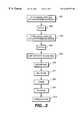
- FIG. 3is a flow chart illustrating an embodiment of the invention in a method of producing the device of FIG. 1 .
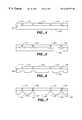
- FIG. 4is a cross sectional illustration of a leadframe material during a first masking step of a leadframe production method according to the invention.
- FIG. 5is a cross sectional illustration of a leadframe material during a first etching step of a leadframe production method according to the invention.
- FIG. 6is a cross sectional illustration of a leadframe material during a second masking step of a leadframe production method according to the invention.
- FIG. 7is a cross sectional illustration of a leadframe material during a second etching step of a leadframe production method according to the invention.
- FIG. 8is a cross sectional illustration of a leadframe produced by the leadframe production portion of the method of FIG. 3 .
- FIG. 9is a top down illustration of the leadframe of FIG. 8 .
- FIG. 10is an illustration of the use of film assisted molding equipment in an embodiment of the invention.
- FIG. 11is a bottom up illustration of the device of FIG. 1 .
- FIG. 12is a bottom up illustration of another embodiment of a device according to the invention.
- FIG. 13is a cross sectional illustration of the device of FIG. 12 .
- FIG. 14is a cross sectional illustration of the device of FIG. 12 .
- FIGS. 1 and 2illustrate a quad flat no-lead (QFN) package, so called because the leads are positioned on all four sides of the package, the exposed (bottom) portions of the leads are coplanar the bottom of the package, and the leads do not extend, or extend only slightly, beyond the area of the package.
- the packageincludes a die pad also having an exposed (bottom) portion that is coplanar with the bottom of the package.
- the top portions of the leadsare coplanar with the top surface of the die pad, and are flat.
- Providing leads on all four sides of the packageallows an improvement in the ratio between pincount and area. Exposing the leads at the bottom of the package allows a reduction in the board area required to mount the package on a PCB. Exposing the die pad at the bottom of the package allows the die pad to be soldered to the PCB to provide an improvement in thermal, electrical, and mechanical reliability. A reduction in the complexity of the lead frame manufacturing process and/or elimination of a post mold etching process are possible given the coplanarity of the bottom of the leads and die pad with the bottom of the package. The mold flash problem can be reduced by using film assisted molding equipment (FAME) during the molding process, as will be subsequently described.
- FAMEfilm assisted molding equipment
- a reduction in the complexity of the wire bon d process through the elimination of downset bondingis possible given the coplanarity of the top of the leads with the top of the die pad.
- a half etch techniquealso to be subsequently described, can be used for the lead frame manufacturing process to allow a reduction in package area.
- the inventioncan be used to provide smaller, less expensive, more manufacturable, more reliable IC packages. Also, it is possible to practice the invention with few changes to an existing assembly infrastructure, and with a short learning curve.
- FIG. 1is a cross sectional illustration of one embodiment of a device according to the invention.
- Device 100includes integrated circuit chip 110 , die pad 120 , leads 130 and 140 , and molding compound 150 .
- Chip 110is affixed to die pad 120 with epoxy 160 .
- Lead 130is electrically connected to chip 110 through bond wire 170
- lead 140is electrically connected to chip 110 through bond wire 180 .
- FIG. 2is a top down illustration of device 100 , with a cutaway view of the interior.
- the portion of lead 130 that is visible from a top down perspective when molding compound 150 is cut awayis top surface 131 of lead 130 .
- the top surface 131 of lead 130is flat, i.e., there are no bends or steps in top surface 131 .
- the portion of lead 130 that is approximately parallel to top surface 131 and furthest from top surface 131is bottom surface 132 .
- the portion of die pad 120 that is coplanar with bottom surface 132 of lead 130is bottom surface 122 of die pad 120 .
- Top surface 141 and bottom surface 142 of lead 140are also shown in FIG. 1 .
- Molding compound 150encapsulates chip 110 , die pad 120 , and leads 130 and 140 such that bottom surface 122 of die pad 120 , bottom surface 132 of lead 130 , and bottom surface 142 of lead 140 are coplanar with bottom surface 152 of molding compound 150 . Therefore, bottom surfaces 122 , 132 , and 142 of die pad 120 , lead 130 , and lead 140 , respectively, are exposed such that they can be electrically connected to a printed circuit board.
- FIG. 3is a flow chart illustrating an embodiment of the invention in a method of producing the IC device of FIG. 1 .
- steps 301 through 305a leadframe is prepared according to a novel “half etch” technique.
- Step 301is described with reference to FIG. 4 .
- etch mask 410is applied to side 421 of leadframe material 420 .
- Leadframe material 420can be any electrically conductive material such as but not limited to copper or a copper alloy.
- Etch mask 410can be any of a variety of materials known in the art of leadframe etching, and can be patterned according to any of a variety of known techniques such as photolithography.
- Step 302is described with reference to FIG. 5 .
- leadframe material 420is etched according to any of a variety of known techniques. The etching process proceeds isotropically and is stopped after the depths of etched areas 501 , 502 , 503 , and 504 are approximately half of the thickness of leadframe material 420 .
- Step 303is described with reference to FIG. 6 .
- etch mask 610is applied to side 622 of leadframe material 420 .
- Step 304is described with reference to FIG. 7 .
- leadframe material 420is etched so that areas 701 , 702 , 703 , and 704 contact areas 501 , 502 , 503 , and 504 .
- Steps 301 through 304produce leadframe 809 as illustrated in the cross sectional view of FIG. 8 and the top down perspective view of FIG. 9 .
- Leadframe 809includes die pad 120 and leads 130 and 140 .
- the half etch processresults in a profile of sidewalls 123 , 124 , 133 , and 143 that includes a relatively straight portion above a relatively concave portion.
- top gap 801 between lead 130 and die pad 120is smaller than bottom gap 802 between lead 130 and die pad 120 . Benefits of this result will be described below.
- leadframe 809is used in the production of device 100 .
- chip 110is affixed to die pad 120 with epoxy 160 .
- Epoxy 160can be conductive or nonconductive within the scope of the present invention.
- leads 130 and 140are wirebonded to chip 110 according to any of a variety of well known wire bonding techniques. Since top surface 121 of die pad 120 is coplanar with top surfaces 131 and 141 of leads 130 and 140 , respectively, the wirebonding process does not require special tooling such as is needed for downset bonding.
- step 307chip 110 and leadframe 809 are encapsulated in molding compound 150 , such as plastic resin, according to any of a variety of molding processes.
- step 307is performed using film assisted molding equipment (FAME) so as to address the mold flash problem.
- FAME technologyis illustrated in FIG. 10 .
- Chip 110 and leadframe 809are encapsulated between top chase 1010 and bottom chase 1020 .
- Film 1030is positioned between leadframe 809 and top chase 1010 during molding. Film 1030 provides a soft cushion to create a tight seal between leadframe 809 and top chase 1010 to reduce the potential for bleeding of molding compound 150 between die pad 120 and leads 130 and 140 .
- step 308molding compound 150 is cured.
- step 309the exposed portions of leadframe 809 are plated with a conductive material such as silver solder or palladium to protect the leadframe from corrosion and to facilitate mounting of device 100 to a PCB.
- Step 309can be performed according to a conventional plating process or a photomechanical plating process, the latter of which provides superior plating tolerance and less bleeding between leads.
- step 310singulation is performed by dicing device 100 away from adjacent device formed using leadframe 809 .
- Step 310can be performed according to a variety of known techniques, which can depend on the specific molding technique used in step 307 .
- pocket moldingwherein each chip is encapsulated in a separate molded body can be used in step 307 , in which case a singulation punch can be used in step 310 to cut the leadframe between adjacent molded bodies.
- a singulation punchcan be used in step 310 to cut the leadframe between adjacent molded bodies.
- One advantage of this pocket molding techniqueis that a portion of the upper surface of the leads, e.g. portion 133 of lead 130 in FIG. 1, is exposed for electrical probing even after mounting.
- block moldingwherein a strip or array of chips is encapsulated within a single molded body, in which case a dicing blade can be used to the body and leadframe between chips.
- Advantages of this block molding techniqueinclude a potential increase in strip or array density and greater flexibility in package body sizes.
- device 100has been produced according to the method illustrated in FIG. 3 .
- benefits of the half etch process discussed abovecan be described.
- the minimum distance between the top surfaces of the die pad and leadsis not limited to the minimum distance between the corresponding bottom surfaces as required to guard against bridging during the surface mount process. Therefore, since the maximum area of the chip is limited by the area of the top surface of the die pad, a larger chip can fit into a package having the same area as a package that is not produced in accordance with the invention. In other words, for a chip having a given area, a potential for a decreased package area exists. Also, the lengths of the wire bonds between the chip and the leads can be reduced, resulting in the potential for improved electrical performance and reliability.
- Another benefitis that the die frame and leads are “locked” into molding compound 150 by virtue of their increasing area, parallel to bottom surface 152 of molding compound 150 , from bottom surface 152 upwards. Therefore, leads are less likely to be pulled out through the bottom of the package during singulation or otherwise. Similarly, mechanical solder joint reliability is improved.
- FIG. 11is a bottom up perspective view of device 100 , showing exposed bottom surfaces 122 , 132 , and 142 of die pad 120 , lead 130 , and lead 140 , respectively.
- Molding compound 150has four sides, side 155 , 156 , 157 , and 158 .
- Leadsare are arranged into four groups, groups 165 , 166 , 167 , and 168 , where group 165 corresponds to side 155 , group 166 corresponds to side 156 , group 167 corresponds to side 157 , and group 168 corresponds to side 158 , each by virtue of its location on the bottom surface 152 of molding compound 150 . More specifically, in this embodiment, leads are arranged into four rows, where each row is parallel to and located approximately alongside a different side of molding compound 150 .
- FIG. 12is a bottom up perspective view of another embodiment of the invention.
- Device 1200includes die pad 1220 , and four groups of leads, groups 1265 , 1266 , 1267 , and 1268 .
- the leadsare grouped according to the location of their exposed bottom surfaces. For example, the exposed bottom surfaces of the leads of group 1265 are arranged into two rows, each row being parallel to and approximately alongside side 1255 of molding compound 1250 .
- FIGS. 13 and 14are cross sectional view of device 1200 .
- FIG. 13is a cross section through die pad 1220 and lead 1230
- FIG. 14is a cross section through die pad 1220 and lead 1270 .
- the cross sectional shapes of die pad 1220 and leads 1230 and 1270have been formed using the half etch process of leadframe production described above.
- the first etch stepcorresponding to step 302 in FIG. 3, is performed using a mask having areas defining the bottom surfaces of die pad 1220 and leads 1230 and 1270 . Therefore, leads having a greater length than those shown in FIG. 1 can be formed, while maintaining the coplanarity of the top surfaces of the die pad and the leads and the coplanarity of the bottom surfaces of the die pad and the leads.
Landscapes
- Engineering & Computer Science (AREA)
- Microelectronics & Electronic Packaging (AREA)
- Physics & Mathematics (AREA)
- Condensed Matter Physics & Semiconductors (AREA)
- General Physics & Mathematics (AREA)
- Computer Hardware Design (AREA)
- Power Engineering (AREA)
- Lead Frames For Integrated Circuits (AREA)
Abstract
Description
Claims (8)
Priority Applications (1)
| Application Number | Priority Date | Filing Date | Title |
|---|---|---|---|
| US09/395,923US6420779B1 (en) | 1999-09-14 | 1999-09-14 | Leadframe based chip scale package and method of producing the same |
Applications Claiming Priority (1)
| Application Number | Priority Date | Filing Date | Title |
|---|---|---|---|
| US09/395,923US6420779B1 (en) | 1999-09-14 | 1999-09-14 | Leadframe based chip scale package and method of producing the same |
Publications (1)
| Publication Number | Publication Date |
|---|---|
| US6420779B1true US6420779B1 (en) | 2002-07-16 |
Family
ID=23565099
Family Applications (1)
| Application Number | Title | Priority Date | Filing Date |
|---|---|---|---|
| US09/395,923Expired - LifetimeUS6420779B1 (en) | 1999-09-14 | 1999-09-14 | Leadframe based chip scale package and method of producing the same |
Country Status (1)
| Country | Link |
|---|---|
| US (1) | US6420779B1 (en) |
Cited By (141)
| Publication number | Priority date | Publication date | Assignee | Title |
|---|---|---|---|---|
| US20020056926A1 (en)* | 2000-01-28 | 2002-05-16 | Advanced Semiconductor Engineering, Inc. Taiwan, R.O.C. | Low-pin-count chip package and manufacturing method thereof |
| US6650004B1 (en)* | 1999-10-28 | 2003-11-18 | Rohm Co., Ltd. | Semiconductor device |
| US6710432B1 (en)* | 2001-11-02 | 2004-03-23 | National Semiconductor Corporation | Integrated circuit package with low inductance ground path and improved thermal capability |
| US6753597B1 (en)* | 1999-12-16 | 2004-06-22 | Amkor Technology, Inc. | Encapsulated semiconductor package including chip paddle and leads |
| US6808961B1 (en)* | 2000-11-28 | 2004-10-26 | National Semiconductor Corporation | Locking of mold compound to conductive substrate panels |
| US6844615B1 (en) | 2003-03-13 | 2005-01-18 | Amkor Technology, Inc. | Leadframe package for semiconductor devices |
| US6846704B2 (en) | 2001-03-27 | 2005-01-25 | Amkor Technology, Inc. | Semiconductor package and method for manufacturing the same |
| US6853059B1 (en)* | 1999-10-15 | 2005-02-08 | Amkor Technology, Inc. | Semiconductor package having improved adhesiveness and ground bonding |
| US6858474B1 (en)* | 2003-12-01 | 2005-02-22 | Agilent Technologies, Inc. | Wire bond package and packaging method |
| US6873041B1 (en) | 2001-11-07 | 2005-03-29 | Amkor Technology, Inc. | Power semiconductor package with strap |
| US20050092508A1 (en)* | 2003-09-24 | 2005-05-05 | Atsushi Kato | Circuit device |
| US6893900B1 (en) | 1998-06-24 | 2005-05-17 | Amkor Technology, Inc. | Method of making an integrated circuit package |
| US20050158917A1 (en)* | 2004-01-13 | 2005-07-21 | Noriyuki Kimura | Manufacturing method for resin sealed semiconductor device |
| US6921967B2 (en) | 2003-09-24 | 2005-07-26 | Amkor Technology, Inc. | Reinforced die pad support structure |
| US6953988B2 (en) | 2000-03-25 | 2005-10-11 | Amkor Technology, Inc. | Semiconductor package |
| US6965157B1 (en) | 1999-11-09 | 2005-11-15 | Amkor Technology, Inc. | Semiconductor package with exposed die pad and body-locking leadframe |
| US20050255634A1 (en)* | 2004-05-11 | 2005-11-17 | Gem Services, Inc. | Chemical-enhanced package singulation process |
| US6967395B1 (en)* | 2001-03-20 | 2005-11-22 | Amkor Technology, Inc. | Mounting for a package containing a chip |
| US6995459B2 (en) | 2002-09-09 | 2006-02-07 | Amkor Technology, Inc. | Semiconductor package with increased number of input and output pins |
| US6998702B1 (en) | 2001-09-19 | 2006-02-14 | Amkor Technology, Inc. | Front edge chamfer feature for fully-molded memory cards |
| US7001799B1 (en) | 2003-03-13 | 2006-02-21 | Amkor Technology, Inc. | Method of making a leadframe for semiconductor devices |
| US7005326B1 (en) | 1998-06-24 | 2006-02-28 | Amkor Technology, Inc. | Method of making an integrated circuit package |
| US7030474B1 (en) | 1998-06-24 | 2006-04-18 | Amkor Technology, Inc. | Plastic integrated circuit package and method and leadframe for making the package |
| US20060084203A1 (en)* | 2004-10-15 | 2006-04-20 | Advanced Semiconductor Engineering Inc. | Method for fabricating quad flat non-leaded package |
| US7045882B2 (en) | 2000-12-29 | 2006-05-16 | Amkor Technology, Inc. | Semiconductor package including flip chip |
| US7045883B1 (en) | 2001-04-04 | 2006-05-16 | Amkor Technology, Inc. | Thermally enhanced chip scale lead on chip semiconductor package and method of making same |
| US7057280B2 (en) | 1998-11-20 | 2006-06-06 | Amkor Technology, Inc. | Leadframe having lead locks to secure leads to encapsulant |
| US7057268B1 (en) | 2004-01-27 | 2006-06-06 | Amkor Technology, Inc. | Cavity case with clip/plug for use on multi-media card |
| US7064009B1 (en) | 2001-04-04 | 2006-06-20 | Amkor Technology, Inc. | Thermally enhanced chip scale lead on chip semiconductor package and method of making same |
| US7071541B1 (en) | 1998-06-24 | 2006-07-04 | Amkor Technology, Inc. | Plastic integrated circuit package and method and leadframe for making the package |
| US7091594B1 (en) | 2004-01-28 | 2006-08-15 | Amkor Technology, Inc. | Leadframe type semiconductor package having reduced inductance and its manufacturing method |
| US7112474B1 (en) | 1998-06-24 | 2006-09-26 | Amkor Technology, Inc. | Method of making an integrated circuit package |
| US7115445B2 (en) | 1999-10-15 | 2006-10-03 | Amkor Technology, Inc. | Semiconductor package having reduced thickness |
| US7122406B1 (en) | 2004-01-02 | 2006-10-17 | Gem Services, Inc. | Semiconductor device package diepad having features formed by electroplating |
| US20060231933A1 (en)* | 2002-04-16 | 2006-10-19 | Cabahug Elsie A | Robust leaded molded packages and methods for forming the same |
| US7138707B1 (en) | 2003-10-21 | 2006-11-21 | Amkor Technology, Inc. | Semiconductor package including leads and conductive posts for providing increased functionality |
| US7144517B1 (en) | 2003-11-07 | 2006-12-05 | Amkor Technology, Inc. | Manufacturing method for leadframe and for semiconductor package using the leadframe |
| US7170150B2 (en) | 2001-03-27 | 2007-01-30 | Amkor Technology, Inc. | Lead frame for semiconductor package |
| US7190062B1 (en) | 2004-06-15 | 2007-03-13 | Amkor Technology, Inc. | Embedded leadframe semiconductor package |
| US7192807B1 (en) | 2002-11-08 | 2007-03-20 | Amkor Technology, Inc. | Wafer level package and fabrication method |
| US20070063322A1 (en)* | 2005-09-22 | 2007-03-22 | Stats Chippac Ltd. | Integrated circuit protruding pad package system |
| US7202554B1 (en) | 2004-08-19 | 2007-04-10 | Amkor Technology, Inc. | Semiconductor package and its manufacturing method |
| US20070093000A1 (en)* | 2005-10-21 | 2007-04-26 | Stats Chippac Ltd. | Pre-molded leadframe and method therefor |
| US7211879B1 (en) | 2003-11-12 | 2007-05-01 | Amkor Technology, Inc. | Semiconductor package with chamfered corners and method of manufacturing the same |
| US7217991B1 (en) | 2004-10-22 | 2007-05-15 | Amkor Technology, Inc. | Fan-in leadframe semiconductor package |
| US20070111379A1 (en)* | 2005-10-21 | 2007-05-17 | Stats Chippac Ltd. | Pre-molded leadframe and method therefor |
| US7245007B1 (en) | 2003-09-18 | 2007-07-17 | Amkor Technology, Inc. | Exposed lead interposer leadframe package |
| US7253503B1 (en) | 1999-11-05 | 2007-08-07 | Amkor Technology, Inc. | Integrated circuit device packages and substrates for making the packages |
| US20070209834A1 (en)* | 2006-03-08 | 2007-09-13 | Stats Chippac Ltd. | Integrated circuit leaded stacked package system |
| US20070210424A1 (en)* | 2006-03-08 | 2007-09-13 | Stats Chippac Ltd. | Integrated circuit package in package system |
| US20070210443A1 (en)* | 2006-03-08 | 2007-09-13 | Stats Chippac Ltd. | Integrated circuit package on package system |
| US20070241423A1 (en)* | 2006-04-14 | 2007-10-18 | Taylor William P | Methods and apparatus for integrated circuit having multiple dies with at least one on chip capacitor |
| US20080034582A1 (en)* | 2006-04-14 | 2008-02-14 | Taylor William P | Methods for sensor having capacitor on chip |
| US7332375B1 (en) | 1998-06-24 | 2008-02-19 | Amkor Technology, Inc. | Method of making an integrated circuit package |
| US7361533B1 (en) | 2002-11-08 | 2008-04-22 | Amkor Technology, Inc. | Stacked embedded leadframe |
| US20080258279A1 (en)* | 2007-04-20 | 2008-10-23 | Chipmos Technologies Inc. | Leadframe for leadless package, structure and manufacturing method using the same |
| US7485952B1 (en) | 2001-09-19 | 2009-02-03 | Amkor Technology, Inc. | Drop resistant bumpers for fully molded memory cards |
| US7507603B1 (en) | 2005-12-02 | 2009-03-24 | Amkor Technology, Inc. | Etch singulated semiconductor package |
| US20090115032A1 (en)* | 2007-11-07 | 2009-05-07 | Zigmund Ramirez Camacho | Integrated circuit package system with dual connectivity |
| US20090194854A1 (en)* | 2008-02-01 | 2009-08-06 | Infineon Technologies Ag | Semiconductor device package and method of making a semiconductor device package |
| US7572681B1 (en) | 2005-12-08 | 2009-08-11 | Amkor Technology, Inc. | Embedded electronic component package |
| US7598598B1 (en) | 2003-02-05 | 2009-10-06 | Amkor Technology, Inc. | Offset etched corner leads for semiconductor package |
| US20100019332A1 (en)* | 2008-07-24 | 2010-01-28 | Taylor William P | Methods and apparatus for integrated circuit having on chip capacitor with eddy current reductions |
| US20100052424A1 (en)* | 2008-08-26 | 2010-03-04 | Taylor William P | Methods and apparatus for integrated circuit having integrated energy storage device |
| US7687899B1 (en) | 2007-08-07 | 2010-03-30 | Amkor Technology, Inc. | Dual laminate package structure with embedded elements |
| US7687893B2 (en) | 2006-12-27 | 2010-03-30 | Amkor Technology, Inc. | Semiconductor package having leadframe with exposed anchor pads |
| US7723210B2 (en) | 2002-11-08 | 2010-05-25 | Amkor Technology, Inc. | Direct-write wafer level chip scale package |
| US7723852B1 (en) | 2008-01-21 | 2010-05-25 | Amkor Technology, Inc. | Stacked semiconductor package and method of making same |
| US7768135B1 (en) | 2008-04-17 | 2010-08-03 | Amkor Technology, Inc. | Semiconductor package with fast power-up cycle and method of making same |
| US7777351B1 (en) | 2007-10-01 | 2010-08-17 | Amkor Technology, Inc. | Thin stacked interposer package |
| US20100213620A1 (en)* | 2009-02-20 | 2010-08-26 | Sumitomo Metal Mining Co., Ltd. | Manufacturing method of substrate for a semiconductor package, manufacturing method of semiconductor package, substrate for a semiconductor package and semiconductor package |
| US7808084B1 (en) | 2008-05-06 | 2010-10-05 | Amkor Technology, Inc. | Semiconductor package with half-etched locking features |
| US7829990B1 (en) | 2007-01-18 | 2010-11-09 | Amkor Technology, Inc. | Stackable semiconductor package including laminate interposer |
| US7847392B1 (en) | 2008-09-30 | 2010-12-07 | Amkor Technology, Inc. | Semiconductor device including leadframe with increased I/O |
| US7847386B1 (en) | 2007-11-05 | 2010-12-07 | Amkor Technology, Inc. | Reduced size stacked semiconductor package and method of making the same |
| US7875963B1 (en) | 2008-11-21 | 2011-01-25 | Amkor Technology, Inc. | Semiconductor device including leadframe having power bars and increased I/O |
| US7902660B1 (en) | 2006-05-24 | 2011-03-08 | Amkor Technology, Inc. | Substrate for semiconductor device and manufacturing method thereof |
| US20110108965A1 (en)* | 2009-11-12 | 2011-05-12 | Hess Kevin J | Semiconductor device package |
| US7956453B1 (en) | 2008-01-16 | 2011-06-07 | Amkor Technology, Inc. | Semiconductor package with patterning layer and method of making same |
| US7960818B1 (en) | 2009-03-04 | 2011-06-14 | Amkor Technology, Inc. | Conformal shield on punch QFN semiconductor package |
| US7968998B1 (en) | 2006-06-21 | 2011-06-28 | Amkor Technology, Inc. | Side leaded, bottom exposed pad and bottom exposed lead fusion quad flat semiconductor package |
| US20110159643A1 (en)* | 2009-12-31 | 2011-06-30 | Siliconware Precision Industries Co., Ltd. | Fabrication method of semiconductor package structure |
| US7977774B2 (en) | 2007-07-10 | 2011-07-12 | Amkor Technology, Inc. | Fusion quad flat semiconductor package |
| US7982298B1 (en) | 2008-12-03 | 2011-07-19 | Amkor Technology, Inc. | Package in package semiconductor device |
| US7982297B1 (en) | 2007-03-06 | 2011-07-19 | Amkor Technology, Inc. | Stackable semiconductor package having partially exposed semiconductor die and method of fabricating the same |
| US7989933B1 (en) | 2008-10-06 | 2011-08-02 | Amkor Technology, Inc. | Increased I/O leadframe and semiconductor device including same |
| US8008758B1 (en) | 2008-10-27 | 2011-08-30 | Amkor Technology, Inc. | Semiconductor device with increased I/O leadframe |
| US8026589B1 (en) | 2009-02-23 | 2011-09-27 | Amkor Technology, Inc. | Reduced profile stackable semiconductor package |
| US8058715B1 (en) | 2009-01-09 | 2011-11-15 | Amkor Technology, Inc. | Package in package device for RF transceiver module |
| US8067821B1 (en) | 2008-04-10 | 2011-11-29 | Amkor Technology, Inc. | Flat semiconductor package with half package molding |
| US8072050B1 (en) | 2008-11-18 | 2011-12-06 | Amkor Technology, Inc. | Semiconductor device with increased I/O leadframe including passive device |
| US8089145B1 (en) | 2008-11-17 | 2012-01-03 | Amkor Technology, Inc. | Semiconductor device including increased capacity leadframe |
| US8089159B1 (en) | 2007-10-03 | 2012-01-03 | Amkor Technology, Inc. | Semiconductor package with increased I/O density and method of making the same |
| US8125064B1 (en) | 2008-07-28 | 2012-02-28 | Amkor Technology, Inc. | Increased I/O semiconductor package and method of making same |
| US8184453B1 (en) | 2008-07-31 | 2012-05-22 | Amkor Technology, Inc. | Increased capacity semiconductor package |
| US8294276B1 (en) | 2010-05-27 | 2012-10-23 | Amkor Technology, Inc. | Semiconductor device and fabricating method thereof |
| US8318287B1 (en) | 1998-06-24 | 2012-11-27 | Amkor Technology, Inc. | Integrated circuit package and method of making the same |
| US8324511B1 (en) | 2010-04-06 | 2012-12-04 | Amkor Technology, Inc. | Through via nub reveal method and structure |
| CN102931161A (en)* | 2012-03-15 | 2013-02-13 | 日月光半导体制造股份有限公司 | Semiconductor package and manufacturing method thereof |
| US20130049183A1 (en)* | 2011-08-31 | 2013-02-28 | Freescale Semiconductor, Inc. | Power device and method of packaging same |
| US8390130B1 (en) | 2011-01-06 | 2013-03-05 | Amkor Technology, Inc. | Through via recessed reveal structure and method |
| US8410585B2 (en) | 2000-04-27 | 2013-04-02 | Amkor Technology, Inc. | Leadframe and semiconductor package made using the leadframe |
| US8440554B1 (en) | 2010-08-02 | 2013-05-14 | Amkor Technology, Inc. | Through via connected backside embedded circuit features structure and method |
| US8487420B1 (en) | 2008-12-08 | 2013-07-16 | Amkor Technology, Inc. | Package in package semiconductor device with film over wire |
| US8487445B1 (en) | 2010-10-05 | 2013-07-16 | Amkor Technology, Inc. | Semiconductor device having through electrodes protruding from dielectric layer |
| US8552548B1 (en) | 2011-11-29 | 2013-10-08 | Amkor Technology, Inc. | Conductive pad on protruding through electrode semiconductor device |
| US8575742B1 (en) | 2009-04-06 | 2013-11-05 | Amkor Technology, Inc. | Semiconductor device with increased I/O leadframe including power bars |
| CN103456644A (en)* | 2012-06-01 | 2013-12-18 | Nxp股份有限公司 | Sleadframe for integrated circuit die packaging in a molded package and a method for preparing such a leadframe |
| US8629539B2 (en) | 2012-01-16 | 2014-01-14 | Allegro Microsystems, Llc | Methods and apparatus for magnetic sensor having non-conductive die paddle |
| US8648450B1 (en) | 2011-01-27 | 2014-02-11 | Amkor Technology, Inc. | Semiconductor device including leadframe with a combination of leads and lands |
| US8674485B1 (en) | 2010-12-08 | 2014-03-18 | Amkor Technology, Inc. | Semiconductor device including leadframe with downsets |
| US8680656B1 (en) | 2009-01-05 | 2014-03-25 | Amkor Technology, Inc. | Leadframe structure for concentrated photovoltaic receiver package |
| US8716069B2 (en)* | 2012-09-28 | 2014-05-06 | Alpha & Omega Semiconductor, Inc. | Semiconductor device employing aluminum alloy lead-frame with anodized aluminum |
| US8791501B1 (en) | 2010-12-03 | 2014-07-29 | Amkor Technology, Inc. | Integrated passive device structure and method |
| US8796561B1 (en) | 2009-10-05 | 2014-08-05 | Amkor Technology, Inc. | Fan out build up substrate stackable package and method |
| US8841758B2 (en) | 2012-06-29 | 2014-09-23 | Freescale Semiconductor, Inc. | Semiconductor device package and method of manufacture |
| US8937381B1 (en) | 2009-12-03 | 2015-01-20 | Amkor Technology, Inc. | Thin stackable package and method |
| US9048298B1 (en) | 2012-03-29 | 2015-06-02 | Amkor Technology, Inc. | Backside warpage control structure and fabrication method |
| US9129943B1 (en) | 2012-03-29 | 2015-09-08 | Amkor Technology, Inc. | Embedded component package and fabrication method |
| US9184118B2 (en) | 2013-05-02 | 2015-11-10 | Amkor Technology Inc. | Micro lead frame structure having reinforcing portions and method |
| US9184148B2 (en) | 2013-10-24 | 2015-11-10 | Amkor Technology, Inc. | Semiconductor package and method therefor |
| US9228860B2 (en) | 2006-07-14 | 2016-01-05 | Allegro Microsystems, Llc | Sensor and method of providing a sensor |
| US9411025B2 (en) | 2013-04-26 | 2016-08-09 | Allegro Microsystems, Llc | Integrated circuit package having a split lead frame and a magnet |
| US9494660B2 (en) | 2012-03-20 | 2016-11-15 | Allegro Microsystems, Llc | Integrated circuit package having a split lead frame |
| US9631481B1 (en) | 2011-01-27 | 2017-04-25 | Amkor Technology, Inc. | Semiconductor device including leadframe with a combination of leads and lands and method |
| US9666788B2 (en) | 2012-03-20 | 2017-05-30 | Allegro Microsystems, Llc | Integrated circuit package having a split lead frame |
| US9673122B2 (en) | 2014-05-02 | 2017-06-06 | Amkor Technology, Inc. | Micro lead frame structure having reinforcing portions and method |
| US9691734B1 (en) | 2009-12-07 | 2017-06-27 | Amkor Technology, Inc. | Method of forming a plurality of electronic component packages |
| US9704725B1 (en) | 2012-03-06 | 2017-07-11 | Amkor Technology, Inc. | Semiconductor device with leadframe configured to facilitate reduced burr formation |
| US9799580B2 (en) | 2016-03-24 | 2017-10-24 | Nxp Usa, Inc. | Semiconductor device package and methods of manufacture thereof |
| US9812588B2 (en) | 2012-03-20 | 2017-11-07 | Allegro Microsystems, Llc | Magnetic field sensor integrated circuit with integral ferromagnetic material |
| US20190035685A1 (en)* | 2016-07-27 | 2019-01-31 | Texas Instruments Incorporated | Sawn Leadless Package Having Wettable Flank Leads |
| US10234513B2 (en) | 2012-03-20 | 2019-03-19 | Allegro Microsystems, Llc | Magnetic field sensor integrated circuit with integral ferromagnetic material |
| US10411498B2 (en) | 2015-10-21 | 2019-09-10 | Allegro Microsystems, Llc | Apparatus and methods for extending sensor integrated circuit operation through a power disturbance |
| US20190295935A1 (en)* | 2015-09-01 | 2019-09-26 | Texas Instruments Incorporated | Flat No-Lead Packages with Electroplated Edges |
| US20190348387A1 (en)* | 2013-03-14 | 2019-11-14 | UTAC Headquarters Pte. Ltd. | Semiconductor packages and methods of packaging semiconductor devices |
| US20200135632A1 (en)* | 2018-10-24 | 2020-04-30 | Texas Instruments Incorporated | Die isolation on a substrate |
| US10811341B2 (en) | 2009-01-05 | 2020-10-20 | Amkor Technology Singapore Holding Pte Ltd. | Semiconductor device with through-mold via |
| US10978897B2 (en) | 2018-04-02 | 2021-04-13 | Allegro Microsystems, Llc | Systems and methods for suppressing undesirable voltage supply artifacts |
| US10991644B2 (en) | 2019-08-22 | 2021-04-27 | Allegro Microsystems, Llc | Integrated circuit package having a low profile |
| US11387203B2 (en)* | 2020-09-08 | 2022-07-12 | Panjit International Inc. | Side wettable package |
Citations (18)
| Publication number | Priority date | Publication date | Assignee | Title |
|---|---|---|---|---|
| JPH0263142A (en) | 1988-08-29 | 1990-03-02 | Fujitsu Ltd | Mold package and its manufacturing method |
| US5363279A (en) | 1991-11-14 | 1994-11-08 | Goldstar Electron Co., Ltd. | Semiconductor package for a semiconductor chip having centrally located bottom bond pads |
| US5428248A (en) | 1992-08-21 | 1995-06-27 | Goldstar Electron Co., Ltd. | Resin molded semiconductor package |
| US5519251A (en) | 1992-10-20 | 1996-05-21 | Fujitsu Limited | Semiconductor device and method of producing the same |
| US5656550A (en) | 1994-08-24 | 1997-08-12 | Fujitsu Limited | Method of producing a semicondutor device having a lead portion with outer connecting terminal |
| US5770888A (en) | 1995-12-29 | 1998-06-23 | Lg Semicon Co., Ltd. | Integrated chip package with reduced dimensions and leads exposed from the top and bottom of the package |
| US5866939A (en) | 1996-01-21 | 1999-02-02 | Anam Semiconductor Inc. | Lead end grid array semiconductor package |
| US5894108A (en) | 1997-02-11 | 1999-04-13 | National Semiconductor Corporation | Plastic package with exposed die |
| US5898212A (en) | 1996-06-14 | 1999-04-27 | Lg Semicon Co., Ltd. | Lead frame and semiconductor package |
| US5900676A (en) | 1996-08-19 | 1999-05-04 | Samsung Electronics Co., Ltd. | Semiconductor device package structure having column leads and a method for production thereof |
| US5929514A (en) | 1998-05-26 | 1999-07-27 | Analog Devices, Inc. | Thermally enhanced lead-under-paddle I.C. leadframe |
| US5933709A (en) | 1996-12-30 | 1999-08-03 | Lg Semicon Co., Ltd | Semiconductor package and method for fabricating same |
| US5939774A (en) | 1994-06-14 | 1999-08-17 | Dai Nippon Printing Co., Ltd. | Semiconductor lead frame |
| US5942794A (en) | 1996-10-22 | 1999-08-24 | Matsushita Electronics Corporation | Plastic encapsulated semiconductor device and method of manufacturing the same |
| US6041495A (en)* | 1997-06-24 | 2000-03-28 | Samsung Electronics Co., Ltd. | Method of manufacturing a circuit board having metal bumps and a semiconductor device package comprising the same |
| US6143981A (en)* | 1998-06-24 | 2000-11-07 | Amkor Technology, Inc. | Plastic integrated circuit package and method and leadframe for making the package |
| US6166430A (en)* | 1998-05-27 | 2000-12-26 | Matsushita Electronics Corporation | Lead frame, method for manufacturing the frame, resin-molded semiconductor device and method for manufacturing the device |
| US6177718B1 (en)* | 1998-04-28 | 2001-01-23 | Kabushiki Kaisha Toshiba | Resin-sealed semiconductor device |
- 1999
- 1999-09-14USUS09/395,923patent/US6420779B1/ennot_activeExpired - Lifetime
Patent Citations (19)
| Publication number | Priority date | Publication date | Assignee | Title |
|---|---|---|---|---|
| JPH0263142A (en) | 1988-08-29 | 1990-03-02 | Fujitsu Ltd | Mold package and its manufacturing method |
| US5363279A (en) | 1991-11-14 | 1994-11-08 | Goldstar Electron Co., Ltd. | Semiconductor package for a semiconductor chip having centrally located bottom bond pads |
| US5428248A (en) | 1992-08-21 | 1995-06-27 | Goldstar Electron Co., Ltd. | Resin molded semiconductor package |
| US5519251A (en) | 1992-10-20 | 1996-05-21 | Fujitsu Limited | Semiconductor device and method of producing the same |
| US5773313A (en) | 1992-10-20 | 1998-06-30 | Fujitsu Limited | Semiconductor device and method of producing the same |
| US5939774A (en) | 1994-06-14 | 1999-08-17 | Dai Nippon Printing Co., Ltd. | Semiconductor lead frame |
| US5656550A (en) | 1994-08-24 | 1997-08-12 | Fujitsu Limited | Method of producing a semicondutor device having a lead portion with outer connecting terminal |
| US5770888A (en) | 1995-12-29 | 1998-06-23 | Lg Semicon Co., Ltd. | Integrated chip package with reduced dimensions and leads exposed from the top and bottom of the package |
| US5866939A (en) | 1996-01-21 | 1999-02-02 | Anam Semiconductor Inc. | Lead end grid array semiconductor package |
| US5898212A (en) | 1996-06-14 | 1999-04-27 | Lg Semicon Co., Ltd. | Lead frame and semiconductor package |
| US5900676A (en) | 1996-08-19 | 1999-05-04 | Samsung Electronics Co., Ltd. | Semiconductor device package structure having column leads and a method for production thereof |
| US5942794A (en) | 1996-10-22 | 1999-08-24 | Matsushita Electronics Corporation | Plastic encapsulated semiconductor device and method of manufacturing the same |
| US5933709A (en) | 1996-12-30 | 1999-08-03 | Lg Semicon Co., Ltd | Semiconductor package and method for fabricating same |
| US5894108A (en) | 1997-02-11 | 1999-04-13 | National Semiconductor Corporation | Plastic package with exposed die |
| US6041495A (en)* | 1997-06-24 | 2000-03-28 | Samsung Electronics Co., Ltd. | Method of manufacturing a circuit board having metal bumps and a semiconductor device package comprising the same |
| US6177718B1 (en)* | 1998-04-28 | 2001-01-23 | Kabushiki Kaisha Toshiba | Resin-sealed semiconductor device |
| US5929514A (en) | 1998-05-26 | 1999-07-27 | Analog Devices, Inc. | Thermally enhanced lead-under-paddle I.C. leadframe |
| US6166430A (en)* | 1998-05-27 | 2000-12-26 | Matsushita Electronics Corporation | Lead frame, method for manufacturing the frame, resin-molded semiconductor device and method for manufacturing the device |
| US6143981A (en)* | 1998-06-24 | 2000-11-07 | Amkor Technology, Inc. | Plastic integrated circuit package and method and leadframe for making the package |
Non-Patent Citations (1)
| Title |
|---|
| Konishi, S., et al., "OFN (Quad Flat Non-Leaded Package)," 4th Symposium on "Microjoining and Assembly Technology in Electronics," Japan Welding Society (Committee of Microjoining), Yokohama, Jan. 29-30, 1998, pp. 149-152 (in Japanese, with English translation). |
Cited By (262)
| Publication number | Priority date | Publication date | Assignee | Title |
|---|---|---|---|---|
| US6893900B1 (en) | 1998-06-24 | 2005-05-17 | Amkor Technology, Inc. | Method of making an integrated circuit package |
| US7112474B1 (en) | 1998-06-24 | 2006-09-26 | Amkor Technology, Inc. | Method of making an integrated circuit package |
| US7030474B1 (en) | 1998-06-24 | 2006-04-18 | Amkor Technology, Inc. | Plastic integrated circuit package and method and leadframe for making the package |
| US7005326B1 (en) | 1998-06-24 | 2006-02-28 | Amkor Technology, Inc. | Method of making an integrated circuit package |
| US8963301B1 (en) | 1998-06-24 | 2015-02-24 | Amkor Technology, Inc. | Integrated circuit package and method of making the same |
| US7560804B1 (en) | 1998-06-24 | 2009-07-14 | Amkor Technology, Inc. | Integrated circuit package and method of making the same |
| US7071541B1 (en) | 1998-06-24 | 2006-07-04 | Amkor Technology, Inc. | Plastic integrated circuit package and method and leadframe for making the package |
| US7332375B1 (en) | 1998-06-24 | 2008-02-19 | Amkor Technology, Inc. | Method of making an integrated circuit package |
| US8853836B1 (en) | 1998-06-24 | 2014-10-07 | Amkor Technology, Inc. | Integrated circuit package and method of making the same |
| US8318287B1 (en) | 1998-06-24 | 2012-11-27 | Amkor Technology, Inc. | Integrated circuit package and method of making the same |
| US9224676B1 (en) | 1998-06-24 | 2015-12-29 | Amkor Technology, Inc. | Integrated circuit package and method of making the same |
| US7057280B2 (en) | 1998-11-20 | 2006-06-06 | Amkor Technology, Inc. | Leadframe having lead locks to secure leads to encapsulant |
| US7564122B2 (en) | 1998-11-20 | 2009-07-21 | Amkor Technology, Inc. | Semiconductor package and method of making using leadframe having lead locks to secure leads to encapsulant |
| US6853059B1 (en)* | 1999-10-15 | 2005-02-08 | Amkor Technology, Inc. | Semiconductor package having improved adhesiveness and ground bonding |
| US20080283979A1 (en)* | 1999-10-15 | 2008-11-20 | Tae Heon Lee | Semiconductor Package Having Reduced Thickness |
| US7067908B2 (en) | 1999-10-15 | 2006-06-27 | Amkor Technology, Inc. | Semiconductor package having improved adhesiveness and ground bonding |
| US7535085B2 (en)* | 1999-10-15 | 2009-05-19 | Amkor Technology, Inc. | Semiconductor package having improved adhesiveness and ground bonding |
| US7321162B1 (en) | 1999-10-15 | 2008-01-22 | Amkor Technology, Inc. | Semiconductor package having reduced thickness |
| US7115445B2 (en) | 1999-10-15 | 2006-10-03 | Amkor Technology, Inc. | Semiconductor package having reduced thickness |
| US20060186517A1 (en)* | 1999-10-15 | 2006-08-24 | Jang Sung S | Semiconductor package having improved adhesiveness and ground bonding |
| US6650004B1 (en)* | 1999-10-28 | 2003-11-18 | Rohm Co., Ltd. | Semiconductor device |
| US7253503B1 (en) | 1999-11-05 | 2007-08-07 | Amkor Technology, Inc. | Integrated circuit device packages and substrates for making the packages |
| US6965157B1 (en) | 1999-11-09 | 2005-11-15 | Amkor Technology, Inc. | Semiconductor package with exposed die pad and body-locking leadframe |
| US6753597B1 (en)* | 1999-12-16 | 2004-06-22 | Amkor Technology, Inc. | Encapsulated semiconductor package including chip paddle and leads |
| US6861295B2 (en)* | 2000-01-28 | 2005-03-01 | Advanced Semiconductor Engineering, Inc. | Low-pin-count chip package and manufacturing method thereof |
| US20020056926A1 (en)* | 2000-01-28 | 2002-05-16 | Advanced Semiconductor Engineering, Inc. Taiwan, R.O.C. | Low-pin-count chip package and manufacturing method thereof |
| US6953988B2 (en) | 2000-03-25 | 2005-10-11 | Amkor Technology, Inc. | Semiconductor package |
| US9362210B2 (en) | 2000-04-27 | 2016-06-07 | Amkor Technology, Inc. | Leadframe and semiconductor package made using the leadframe |
| US8410585B2 (en) | 2000-04-27 | 2013-04-02 | Amkor Technology, Inc. | Leadframe and semiconductor package made using the leadframe |
| US6808961B1 (en)* | 2000-11-28 | 2004-10-26 | National Semiconductor Corporation | Locking of mold compound to conductive substrate panels |
| US7045882B2 (en) | 2000-12-29 | 2006-05-16 | Amkor Technology, Inc. | Semiconductor package including flip chip |
| US6967395B1 (en)* | 2001-03-20 | 2005-11-22 | Amkor Technology, Inc. | Mounting for a package containing a chip |
| US7521294B2 (en) | 2001-03-27 | 2009-04-21 | Amkor Technology, Inc. | Lead frame for semiconductor package |
| US7170150B2 (en) | 2001-03-27 | 2007-01-30 | Amkor Technology, Inc. | Lead frame for semiconductor package |
| US6846704B2 (en) | 2001-03-27 | 2005-01-25 | Amkor Technology, Inc. | Semiconductor package and method for manufacturing the same |
| US7928542B2 (en) | 2001-03-27 | 2011-04-19 | Amkor Technology, Inc. | Lead frame for semiconductor package |
| US8102037B2 (en) | 2001-03-27 | 2012-01-24 | Amkor Technology, Inc. | Leadframe for semiconductor package |
| US7064009B1 (en) | 2001-04-04 | 2006-06-20 | Amkor Technology, Inc. | Thermally enhanced chip scale lead on chip semiconductor package and method of making same |
| US7045883B1 (en) | 2001-04-04 | 2006-05-16 | Amkor Technology, Inc. | Thermally enhanced chip scale lead on chip semiconductor package and method of making same |
| US7176062B1 (en) | 2001-09-19 | 2007-02-13 | Amkor Technology, Inc. | Lead-frame method and assembly for interconnecting circuits within a circuit module |
| US6998702B1 (en) | 2001-09-19 | 2006-02-14 | Amkor Technology, Inc. | Front edge chamfer feature for fully-molded memory cards |
| US7485952B1 (en) | 2001-09-19 | 2009-02-03 | Amkor Technology, Inc. | Drop resistant bumpers for fully molded memory cards |
| US6710432B1 (en)* | 2001-11-02 | 2004-03-23 | National Semiconductor Corporation | Integrated circuit package with low inductance ground path and improved thermal capability |
| US6873041B1 (en) | 2001-11-07 | 2005-03-29 | Amkor Technology, Inc. | Power semiconductor package with strap |
| US20060231933A1 (en)* | 2002-04-16 | 2006-10-19 | Cabahug Elsie A | Robust leaded molded packages and methods for forming the same |
| US7560311B2 (en)* | 2002-04-16 | 2009-07-14 | Fairchild Semiconductor Corporation | Robust leaded molded packages and methods for forming the same |
| US7211471B1 (en) | 2002-09-09 | 2007-05-01 | Amkor Technology, Inc. | Exposed lead QFP package fabricated through the use of a partial saw process |
| US6995459B2 (en) | 2002-09-09 | 2006-02-07 | Amkor Technology, Inc. | Semiconductor package with increased number of input and output pins |
| US8710649B1 (en) | 2002-11-08 | 2014-04-29 | Amkor Technology, Inc. | Wafer level package and fabrication method |
| US8952522B1 (en) | 2002-11-08 | 2015-02-10 | Amkor Technology, Inc. | Wafer level package and fabrication method |
| US7714431B1 (en) | 2002-11-08 | 2010-05-11 | Amkor Technology, Inc. | Electronic component package comprising fan-out and fan-in traces |
| US8501543B1 (en) | 2002-11-08 | 2013-08-06 | Amkor Technology, Inc. | Direct-write wafer level chip scale package |
| US7692286B1 (en) | 2002-11-08 | 2010-04-06 | Amkor Technology, Inc. | Two-sided fan-out wafer escape package |
| US7247523B1 (en) | 2002-11-08 | 2007-07-24 | Amkor Technology, Inc. | Two-sided wafer escape package |
| US9871015B1 (en) | 2002-11-08 | 2018-01-16 | Amkor Technology, Inc. | Wafer level package and fabrication method |
| US8691632B1 (en) | 2002-11-08 | 2014-04-08 | Amkor Technology, Inc. | Wafer level package and fabrication method |
| US9406645B1 (en) | 2002-11-08 | 2016-08-02 | Amkor Technology, Inc. | Wafer level package and fabrication method |
| US10665567B1 (en) | 2002-11-08 | 2020-05-26 | Amkor Technology, Inc. | Wafer level package and fabrication method |
| US7932595B1 (en) | 2002-11-08 | 2011-04-26 | Amkor Technology, Inc. | Electronic component package comprising fan-out traces |
| US7723210B2 (en) | 2002-11-08 | 2010-05-25 | Amkor Technology, Inc. | Direct-write wafer level chip scale package |
| US8188584B1 (en) | 2002-11-08 | 2012-05-29 | Amkor Technology, Inc. | Direct-write wafer level chip scale package |
| US8298866B1 (en) | 2002-11-08 | 2012-10-30 | Amkor Technology, Inc. | Wafer level package and fabrication method |
| US7192807B1 (en) | 2002-11-08 | 2007-03-20 | Amkor Technology, Inc. | Wafer level package and fabrication method |
| US8119455B1 (en) | 2002-11-08 | 2012-02-21 | Amkor Technology, Inc. | Wafer level package fabrication method |
| US7361533B1 (en) | 2002-11-08 | 2008-04-22 | Amkor Technology, Inc. | Stacked embedded leadframe |
| US8486764B1 (en) | 2002-11-08 | 2013-07-16 | Amkor Technology, Inc. | Wafer level package and fabrication method |
| US7420272B1 (en) | 2002-11-08 | 2008-09-02 | Amkor Technology, Inc. | Two-sided wafer escape package |
| US9054117B1 (en) | 2002-11-08 | 2015-06-09 | Amkor Technology, Inc. | Wafer level package and fabrication method |
| US7598598B1 (en) | 2003-02-05 | 2009-10-06 | Amkor Technology, Inc. | Offset etched corner leads for semiconductor package |
| US7001799B1 (en) | 2003-03-13 | 2006-02-21 | Amkor Technology, Inc. | Method of making a leadframe for semiconductor devices |
| US6844615B1 (en) | 2003-03-13 | 2005-01-18 | Amkor Technology, Inc. | Leadframe package for semiconductor devices |
| US7245007B1 (en) | 2003-09-18 | 2007-07-17 | Amkor Technology, Inc. | Exposed lead interposer leadframe package |
| US20050092508A1 (en)* | 2003-09-24 | 2005-05-05 | Atsushi Kato | Circuit device |
| US6921967B2 (en) | 2003-09-24 | 2005-07-26 | Amkor Technology, Inc. | Reinforced die pad support structure |
| US7138707B1 (en) | 2003-10-21 | 2006-11-21 | Amkor Technology, Inc. | Semiconductor package including leads and conductive posts for providing increased functionality |
| US7144517B1 (en) | 2003-11-07 | 2006-12-05 | Amkor Technology, Inc. | Manufacturing method for leadframe and for semiconductor package using the leadframe |
| US7214326B1 (en) | 2003-11-07 | 2007-05-08 | Amkor Technology, Inc. | Increased capacity leadframe and semiconductor package using the same |
| US7211879B1 (en) | 2003-11-12 | 2007-05-01 | Amkor Technology, Inc. | Semiconductor package with chamfered corners and method of manufacturing the same |
| US6858474B1 (en)* | 2003-12-01 | 2005-02-22 | Agilent Technologies, Inc. | Wire bond package and packaging method |
| US20110003439A1 (en)* | 2004-01-02 | 2011-01-06 | GEM Services | Semiconductor device package having features formed by electroplating |
| US7122406B1 (en) | 2004-01-02 | 2006-10-17 | Gem Services, Inc. | Semiconductor device package diepad having features formed by electroplating |
| US20050158917A1 (en)* | 2004-01-13 | 2005-07-21 | Noriyuki Kimura | Manufacturing method for resin sealed semiconductor device |
| US7271035B2 (en)* | 2004-01-13 | 2007-09-18 | Seiko Instruments Inc. | Manufacturing method for resin sealed semiconductor device |
| US7057268B1 (en) | 2004-01-27 | 2006-06-06 | Amkor Technology, Inc. | Cavity case with clip/plug for use on multi-media card |
| US7091594B1 (en) | 2004-01-28 | 2006-08-15 | Amkor Technology, Inc. | Leadframe type semiconductor package having reduced inductance and its manufacturing method |
| US7553700B2 (en) | 2004-05-11 | 2009-06-30 | Gem Services, Inc. | Chemical-enhanced package singulation process |
| US20050255634A1 (en)* | 2004-05-11 | 2005-11-17 | Gem Services, Inc. | Chemical-enhanced package singulation process |
| US7190062B1 (en) | 2004-06-15 | 2007-03-13 | Amkor Technology, Inc. | Embedded leadframe semiconductor package |
| US7202554B1 (en) | 2004-08-19 | 2007-04-10 | Amkor Technology, Inc. | Semiconductor package and its manufacturing method |
| US20060084203A1 (en)* | 2004-10-15 | 2006-04-20 | Advanced Semiconductor Engineering Inc. | Method for fabricating quad flat non-leaded package |
| US7351612B2 (en)* | 2004-10-15 | 2008-04-01 | Advance Semiconductor Engineering Inc. | Method for fabricating quad flat non-leaded package |
| US7217991B1 (en) | 2004-10-22 | 2007-05-15 | Amkor Technology, Inc. | Fan-in leadframe semiconductor package |
| US7473584B1 (en) | 2004-10-22 | 2009-01-06 | Amkor Technology, Inc. | Method for fabricating a fan-in leadframe semiconductor package |
| US7968377B2 (en) | 2005-09-22 | 2011-06-28 | Stats Chippac Ltd. | Integrated circuit protruding pad package system |
| US20070063322A1 (en)* | 2005-09-22 | 2007-03-22 | Stats Chippac Ltd. | Integrated circuit protruding pad package system |
| US20110233744A1 (en)* | 2005-09-22 | 2011-09-29 | Seng Guan Chow | Integrated circuit protruding pad package system and method for manufacturing thereof |
| US8587098B2 (en) | 2005-09-22 | 2013-11-19 | Stats Chippac Ltd. | Integrated circuit protruding pad package system and method for manufacturing thereof |
| US20070093000A1 (en)* | 2005-10-21 | 2007-04-26 | Stats Chippac Ltd. | Pre-molded leadframe and method therefor |
| US20070111379A1 (en)* | 2005-10-21 | 2007-05-17 | Stats Chippac Ltd. | Pre-molded leadframe and method therefor |
| US7399658B2 (en) | 2005-10-21 | 2008-07-15 | Stats Chippac Ltd. | Pre-molded leadframe and method therefor |
| US7507603B1 (en) | 2005-12-02 | 2009-03-24 | Amkor Technology, Inc. | Etch singulated semiconductor package |
| US7732899B1 (en) | 2005-12-02 | 2010-06-08 | Amkor Technology, Inc. | Etch singulated semiconductor package |
| US7977163B1 (en) | 2005-12-08 | 2011-07-12 | Amkor Technology, Inc. | Embedded electronic component package fabrication method |
| US7572681B1 (en) | 2005-12-08 | 2009-08-11 | Amkor Technology, Inc. | Embedded electronic component package |
| US20070210443A1 (en)* | 2006-03-08 | 2007-09-13 | Stats Chippac Ltd. | Integrated circuit package on package system |
| US8513542B2 (en) | 2006-03-08 | 2013-08-20 | Stats Chippac Ltd. | Integrated circuit leaded stacked package system |
| US7981702B2 (en) | 2006-03-08 | 2011-07-19 | Stats Chippac Ltd. | Integrated circuit package in package system |
| US20070210424A1 (en)* | 2006-03-08 | 2007-09-13 | Stats Chippac Ltd. | Integrated circuit package in package system |
| US20070209834A1 (en)* | 2006-03-08 | 2007-09-13 | Stats Chippac Ltd. | Integrated circuit leaded stacked package system |
| US7986043B2 (en) | 2006-03-08 | 2011-07-26 | Stats Chippac Ltd. | Integrated circuit package on package system |
| US8164172B2 (en) | 2006-03-08 | 2012-04-24 | Stats Chippac Ltd. | Integrated circuit package in package system |
| US7687882B2 (en) | 2006-04-14 | 2010-03-30 | Allegro Microsystems, Inc. | Methods and apparatus for integrated circuit having multiple dies with at least one on chip capacitor |
| US20070241423A1 (en)* | 2006-04-14 | 2007-10-18 | Taylor William P | Methods and apparatus for integrated circuit having multiple dies with at least one on chip capacitor |
| US7676914B2 (en) | 2006-04-14 | 2010-03-16 | Allegro Microsystems, Inc. | Methods for sensor having capacitor on chip |
| US20080034582A1 (en)* | 2006-04-14 | 2008-02-14 | Taylor William P | Methods for sensor having capacitor on chip |
| US7902660B1 (en) | 2006-05-24 | 2011-03-08 | Amkor Technology, Inc. | Substrate for semiconductor device and manufacturing method thereof |
| US7968998B1 (en) | 2006-06-21 | 2011-06-28 | Amkor Technology, Inc. | Side leaded, bottom exposed pad and bottom exposed lead fusion quad flat semiconductor package |
| US8441110B1 (en) | 2006-06-21 | 2013-05-14 | Amkor Technology, Inc. | Side leaded, bottom exposed pad and bottom exposed lead fusion quad flat semiconductor package |
| US9228860B2 (en) | 2006-07-14 | 2016-01-05 | Allegro Microsystems, Llc | Sensor and method of providing a sensor |
| US8089141B1 (en) | 2006-12-27 | 2012-01-03 | Amkor Technology, Inc. | Semiconductor package having leadframe with exposed anchor pads |
| US7687893B2 (en) | 2006-12-27 | 2010-03-30 | Amkor Technology, Inc. | Semiconductor package having leadframe with exposed anchor pads |
| US7829990B1 (en) | 2007-01-18 | 2010-11-09 | Amkor Technology, Inc. | Stackable semiconductor package including laminate interposer |
| US7982297B1 (en) | 2007-03-06 | 2011-07-19 | Amkor Technology, Inc. | Stackable semiconductor package having partially exposed semiconductor die and method of fabricating the same |
| US8106494B2 (en)* | 2007-04-20 | 2012-01-31 | Chipmos Technologies Inc. | Leadframe for leadless package, structure and manufacturing method using the same |
| US20110133322A1 (en)* | 2007-04-20 | 2011-06-09 | Chipmos Technologies Inc. | Leadframe for leadless package, structure and manufacturing method using the same |
| US7902649B2 (en)* | 2007-04-20 | 2011-03-08 | Chipmos Technologies Inc. | Leadframe for leadless package, structure and manufacturing method using the same |
| US20110136299A1 (en)* | 2007-04-20 | 2011-06-09 | Chipmos Technologies Inc. | Leadframe for leadless package, structure and manufacturing method using the same |
| US8105876B2 (en)* | 2007-04-20 | 2012-01-31 | Chipmos Technologies Inc. | Leadframe for leadless package, structure and manufacturing method using the same |
| US20080258279A1 (en)* | 2007-04-20 | 2008-10-23 | Chipmos Technologies Inc. | Leadframe for leadless package, structure and manufacturing method using the same |
| US8304866B1 (en) | 2007-07-10 | 2012-11-06 | Amkor Technology, Inc. | Fusion quad flat semiconductor package |
| US7977774B2 (en) | 2007-07-10 | 2011-07-12 | Amkor Technology, Inc. | Fusion quad flat semiconductor package |
| US7872343B1 (en) | 2007-08-07 | 2011-01-18 | Amkor Technology, Inc. | Dual laminate package structure with embedded elements |
| US7687899B1 (en) | 2007-08-07 | 2010-03-30 | Amkor Technology, Inc. | Dual laminate package structure with embedded elements |
| US8283767B1 (en) | 2007-08-07 | 2012-10-09 | Amkor Technology, Inc. | Dual laminate package structure with embedded elements |
| US7777351B1 (en) | 2007-10-01 | 2010-08-17 | Amkor Technology, Inc. | Thin stacked interposer package |
| US8319338B1 (en) | 2007-10-01 | 2012-11-27 | Amkor Technology, Inc. | Thin stacked interposer package |
| US8227921B1 (en) | 2007-10-03 | 2012-07-24 | Amkor Technology, Inc. | Semiconductor package with increased I/O density and method of making same |
| US8089159B1 (en) | 2007-10-03 | 2012-01-03 | Amkor Technology, Inc. | Semiconductor package with increased I/O density and method of making the same |
| US7847386B1 (en) | 2007-11-05 | 2010-12-07 | Amkor Technology, Inc. | Reduced size stacked semiconductor package and method of making the same |
| US20090115032A1 (en)* | 2007-11-07 | 2009-05-07 | Zigmund Ramirez Camacho | Integrated circuit package system with dual connectivity |
| US7977782B2 (en) | 2007-11-07 | 2011-07-12 | Stats Chippac Ltd. | Integrated circuit package system with dual connectivity |
| US7956453B1 (en) | 2008-01-16 | 2011-06-07 | Amkor Technology, Inc. | Semiconductor package with patterning layer and method of making same |
| US8729710B1 (en) | 2008-01-16 | 2014-05-20 | Amkor Technology, Inc. | Semiconductor package with patterning layer and method of making same |
| US7723852B1 (en) | 2008-01-21 | 2010-05-25 | Amkor Technology, Inc. | Stacked semiconductor package and method of making same |
| US7906855B1 (en) | 2008-01-21 | 2011-03-15 | Amkor Technology, Inc. | Stacked semiconductor package and method of making same |
| US8912635B2 (en) | 2008-02-01 | 2014-12-16 | Infineon Technologies Ag | Semiconductor device package and method of making a semiconductor device package |
| US8084299B2 (en) | 2008-02-01 | 2011-12-27 | Infineon Technologies Ag | Semiconductor device package and method of making a semiconductor device package |
| US20090194854A1 (en)* | 2008-02-01 | 2009-08-06 | Infineon Technologies Ag | Semiconductor device package and method of making a semiconductor device package |
| US8067821B1 (en) | 2008-04-10 | 2011-11-29 | Amkor Technology, Inc. | Flat semiconductor package with half package molding |
| US8084868B1 (en) | 2008-04-17 | 2011-12-27 | Amkor Technology, Inc. | Semiconductor package with fast power-up cycle and method of making same |
| US7768135B1 (en) | 2008-04-17 | 2010-08-03 | Amkor Technology, Inc. | Semiconductor package with fast power-up cycle and method of making same |
| US7808084B1 (en) | 2008-05-06 | 2010-10-05 | Amkor Technology, Inc. | Semiconductor package with half-etched locking features |
| US8093670B2 (en) | 2008-07-24 | 2012-01-10 | Allegro Microsystems, Inc. | Methods and apparatus for integrated circuit having on chip capacitor with eddy current reductions |
| US20100019332A1 (en)* | 2008-07-24 | 2010-01-28 | Taylor William P | Methods and apparatus for integrated circuit having on chip capacitor with eddy current reductions |
| US8125064B1 (en) | 2008-07-28 | 2012-02-28 | Amkor Technology, Inc. | Increased I/O semiconductor package and method of making same |
| US8184453B1 (en) | 2008-07-31 | 2012-05-22 | Amkor Technology, Inc. | Increased capacity semiconductor package |
| US20100052424A1 (en)* | 2008-08-26 | 2010-03-04 | Taylor William P | Methods and apparatus for integrated circuit having integrated energy storage device |
| US7847392B1 (en) | 2008-09-30 | 2010-12-07 | Amkor Technology, Inc. | Semiconductor device including leadframe with increased I/O |
| US8299602B1 (en) | 2008-09-30 | 2012-10-30 | Amkor Technology, Inc. | Semiconductor device including leadframe with increased I/O |
| US7989933B1 (en) | 2008-10-06 | 2011-08-02 | Amkor Technology, Inc. | Increased I/O leadframe and semiconductor device including same |
| US8432023B1 (en) | 2008-10-06 | 2013-04-30 | Amkor Technology, Inc. | Increased I/O leadframe and semiconductor device including same |
| US8008758B1 (en) | 2008-10-27 | 2011-08-30 | Amkor Technology, Inc. | Semiconductor device with increased I/O leadframe |
| US8823152B1 (en) | 2008-10-27 | 2014-09-02 | Amkor Technology, Inc. | Semiconductor device with increased I/O leadframe |
| US8089145B1 (en) | 2008-11-17 | 2012-01-03 | Amkor Technology, Inc. | Semiconductor device including increased capacity leadframe |
| US8072050B1 (en) | 2008-11-18 | 2011-12-06 | Amkor Technology, Inc. | Semiconductor device with increased I/O leadframe including passive device |
| US7875963B1 (en) | 2008-11-21 | 2011-01-25 | Amkor Technology, Inc. | Semiconductor device including leadframe having power bars and increased I/O |
| US8188579B1 (en) | 2008-11-21 | 2012-05-29 | Amkor Technology, Inc. | Semiconductor device including leadframe having power bars and increased I/O |
| US7982298B1 (en) | 2008-12-03 | 2011-07-19 | Amkor Technology, Inc. | Package in package semiconductor device |
| US8487420B1 (en) | 2008-12-08 | 2013-07-16 | Amkor Technology, Inc. | Package in package semiconductor device with film over wire |
| US8680656B1 (en) | 2009-01-05 | 2014-03-25 | Amkor Technology, Inc. | Leadframe structure for concentrated photovoltaic receiver package |
| US10811341B2 (en) | 2009-01-05 | 2020-10-20 | Amkor Technology Singapore Holding Pte Ltd. | Semiconductor device with through-mold via |
| US11869829B2 (en) | 2009-01-05 | 2024-01-09 | Amkor Technology Singapore Holding Pte. Ltd. | Semiconductor device with through-mold via |
| US8058715B1 (en) | 2009-01-09 | 2011-11-15 | Amkor Technology, Inc. | Package in package device for RF transceiver module |
| US8558365B1 (en) | 2009-01-09 | 2013-10-15 | Amkor Technology, Inc. | Package in package device for RF transceiver module |
| US8188588B2 (en)* | 2009-02-20 | 2012-05-29 | Sumitomo Metal Mining Co., Ltd. | Manufacturing method of substrate for a semiconductor package, manufacturing method of semiconductor package, substrate for a semiconductor package and semiconductor package |
| TWI420636B (en)* | 2009-02-20 | 2013-12-21 | Sumitomo Metal Mining Co | Method for manufacturing a substrate for a semiconductor device, a method for manufacturing a semiconductor device, a substrate for a semiconductor device, and a semiconductor device |
| US9054116B2 (en) | 2009-02-20 | 2015-06-09 | Sh Materials Co., Ltd. | Manufacturing method of substrate for a semiconductor package, manufacturing method of semiconductor package, substrate for a semiconductor package and semiconductor package |
| US20100213620A1 (en)* | 2009-02-20 | 2010-08-26 | Sumitomo Metal Mining Co., Ltd. | Manufacturing method of substrate for a semiconductor package, manufacturing method of semiconductor package, substrate for a semiconductor package and semiconductor package |
| US8026589B1 (en) | 2009-02-23 | 2011-09-27 | Amkor Technology, Inc. | Reduced profile stackable semiconductor package |
| US8729682B1 (en) | 2009-03-04 | 2014-05-20 | Amkor Technology, Inc. | Conformal shield on punch QFN semiconductor package |
| US7960818B1 (en) | 2009-03-04 | 2011-06-14 | Amkor Technology, Inc. | Conformal shield on punch QFN semiconductor package |
| US8575742B1 (en) | 2009-04-06 | 2013-11-05 | Amkor Technology, Inc. | Semiconductor device with increased I/O leadframe including power bars |
| US8796561B1 (en) | 2009-10-05 | 2014-08-05 | Amkor Technology, Inc. | Fan out build up substrate stackable package and method |
| US20110108965A1 (en)* | 2009-11-12 | 2011-05-12 | Hess Kevin J | Semiconductor device package |
| US8501539B2 (en) | 2009-11-12 | 2013-08-06 | Freescale Semiconductor, Inc. | Semiconductor device package |
| US8937381B1 (en) | 2009-12-03 | 2015-01-20 | Amkor Technology, Inc. | Thin stackable package and method |
| US10546833B2 (en) | 2009-12-07 | 2020-01-28 | Amkor Technology, Inc. | Method of forming a plurality of electronic component packages |
| US9691734B1 (en) | 2009-12-07 | 2017-06-27 | Amkor Technology, Inc. | Method of forming a plurality of electronic component packages |
| US20110159643A1 (en)* | 2009-12-31 | 2011-06-30 | Siliconware Precision Industries Co., Ltd. | Fabrication method of semiconductor package structure |
| US8981575B2 (en) | 2009-12-31 | 2015-03-17 | Siliconware Precision Industries Co., Ltd. | Semiconductor package structure |
| US20110156227A1 (en)* | 2009-12-31 | 2011-06-30 | Siliconware Precision Industries Co., Ltd. | Semiconductor package structure |
| US8421199B2 (en) | 2009-12-31 | 2013-04-16 | Siliconware Precision Industries Co., Ltd. | Semiconductor package structure |
| US8304268B2 (en) | 2009-12-31 | 2012-11-06 | Siliconware Precision Industries Co., Ltd. | Fabrication method of semiconductor package structure |
| US8324511B1 (en) | 2010-04-06 | 2012-12-04 | Amkor Technology, Inc. | Through via nub reveal method and structure |
| US9324614B1 (en) | 2010-04-06 | 2016-04-26 | Amkor Technology, Inc. | Through via nub reveal method and structure |
| US8294276B1 (en) | 2010-05-27 | 2012-10-23 | Amkor Technology, Inc. | Semiconductor device and fabricating method thereof |
| US9159672B1 (en) | 2010-08-02 | 2015-10-13 | Amkor Technology, Inc. | Through via connected backside embedded circuit features structure and method |
| US8440554B1 (en) | 2010-08-02 | 2013-05-14 | Amkor Technology, Inc. | Through via connected backside embedded circuit features structure and method |
| US8900995B1 (en) | 2010-10-05 | 2014-12-02 | Amkor Technology, Inc. | Semiconductor device and manufacturing method thereof |
| US8487445B1 (en) | 2010-10-05 | 2013-07-16 | Amkor Technology, Inc. | Semiconductor device having through electrodes protruding from dielectric layer |
| US8791501B1 (en) | 2010-12-03 | 2014-07-29 | Amkor Technology, Inc. | Integrated passive device structure and method |
| US8674485B1 (en) | 2010-12-08 | 2014-03-18 | Amkor Technology, Inc. | Semiconductor device including leadframe with downsets |
| US8390130B1 (en) | 2011-01-06 | 2013-03-05 | Amkor Technology, Inc. | Through via recessed reveal structure and method |
| US9082833B1 (en) | 2011-01-06 | 2015-07-14 | Amkor Technology, Inc. | Through via recessed reveal structure and method |
| US9631481B1 (en) | 2011-01-27 | 2017-04-25 | Amkor Technology, Inc. | Semiconductor device including leadframe with a combination of leads and lands and method |
| US9275939B1 (en) | 2011-01-27 | 2016-03-01 | Amkor Technology, Inc. | Semiconductor device including leadframe with a combination of leads and lands and method |
| US9508631B1 (en) | 2011-01-27 | 2016-11-29 | Amkor Technology, Inc. | Semiconductor device including leadframe with a combination of leads and lands and method |
| US8648450B1 (en) | 2011-01-27 | 2014-02-11 | Amkor Technology, Inc. | Semiconductor device including leadframe with a combination of leads and lands |
| US9978695B1 (en) | 2011-01-27 | 2018-05-22 | Amkor Technology, Inc. | Semiconductor device including leadframe with a combination of leads and lands and method |
| US8709875B2 (en)* | 2011-08-31 | 2014-04-29 | Freescale Semiconductor, Inc. | Power device and method of packaging same |
| US20130049183A1 (en)* | 2011-08-31 | 2013-02-28 | Freescale Semiconductor, Inc. | Power device and method of packaging same |
| US8552548B1 (en) | 2011-11-29 | 2013-10-08 | Amkor Technology, Inc. | Conductive pad on protruding through electrode semiconductor device |
| US11043458B2 (en) | 2011-11-29 | 2021-06-22 | Amkor Technology Singapore Holding Pte. Ltd. | Method of manufacturing an electronic device comprising a conductive pad on a protruding-through electrode |
| US10410967B1 (en) | 2011-11-29 | 2019-09-10 | Amkor Technology, Inc. | Electronic device comprising a conductive pad on a protruding-through electrode |
| US9431323B1 (en) | 2011-11-29 | 2016-08-30 | Amkor Technology, Inc. | Conductive pad on protruding through electrode |
| US9947623B1 (en) | 2011-11-29 | 2018-04-17 | Amkor Technology, Inc. | Semiconductor device comprising a conductive pad on a protruding-through electrode |
| US8981572B1 (en) | 2011-11-29 | 2015-03-17 | Amkor Technology, Inc. | Conductive pad on protruding through electrode semiconductor device |
| US9620705B2 (en) | 2012-01-16 | 2017-04-11 | Allegro Microsystems, Llc | Methods and apparatus for magnetic sensor having non-conductive die paddle |
| US10333055B2 (en) | 2012-01-16 | 2019-06-25 | Allegro Microsystems, Llc | Methods for magnetic sensor having non-conductive die paddle |
| US9299915B2 (en) | 2012-01-16 | 2016-03-29 | Allegro Microsystems, Llc | Methods and apparatus for magnetic sensor having non-conductive die paddle |
| US8629539B2 (en) | 2012-01-16 | 2014-01-14 | Allegro Microsystems, Llc | Methods and apparatus for magnetic sensor having non-conductive die paddle |
| US10090228B1 (en) | 2012-03-06 | 2018-10-02 | Amkor Technology, Inc. | Semiconductor device with leadframe configured to facilitate reduced burr formation |
| US9704725B1 (en) | 2012-03-06 | 2017-07-11 | Amkor Technology, Inc. | Semiconductor device with leadframe configured to facilitate reduced burr formation |
| CN102931161A (en)* | 2012-03-15 | 2013-02-13 | 日月光半导体制造股份有限公司 | Semiconductor package and manufacturing method thereof |
| US11444209B2 (en) | 2012-03-20 | 2022-09-13 | Allegro Microsystems, Llc | Magnetic field sensor integrated circuit with an integrated coil enclosed with a semiconductor die by a mold material |
| US9666788B2 (en) | 2012-03-20 | 2017-05-30 | Allegro Microsystems, Llc | Integrated circuit package having a split lead frame |
| US11961920B2 (en) | 2012-03-20 | 2024-04-16 | Allegro Microsystems, Llc | Integrated circuit package with magnet having a channel |
| US10916665B2 (en) | 2012-03-20 | 2021-02-09 | Allegro Microsystems, Llc | Magnetic field sensor integrated circuit with an integrated coil |
| US10234513B2 (en) | 2012-03-20 | 2019-03-19 | Allegro Microsystems, Llc | Magnetic field sensor integrated circuit with integral ferromagnetic material |
| US9812588B2 (en) | 2012-03-20 | 2017-11-07 | Allegro Microsystems, Llc | Magnetic field sensor integrated circuit with integral ferromagnetic material |
| US11677032B2 (en) | 2012-03-20 | 2023-06-13 | Allegro Microsystems, Llc | Sensor integrated circuit with integrated coil and element in central region of mold material |
| US9494660B2 (en) | 2012-03-20 | 2016-11-15 | Allegro Microsystems, Llc | Integrated circuit package having a split lead frame |
| US11828819B2 (en) | 2012-03-20 | 2023-11-28 | Allegro Microsystems, Llc | Magnetic field sensor integrated circuit with integral ferromagnetic material |
| US10230006B2 (en) | 2012-03-20 | 2019-03-12 | Allegro Microsystems, Llc | Magnetic field sensor integrated circuit with an electromagnetic suppressor |
| US9129943B1 (en) | 2012-03-29 | 2015-09-08 | Amkor Technology, Inc. | Embedded component package and fabrication method |
| US10014240B1 (en) | 2012-03-29 | 2018-07-03 | Amkor Technology, Inc. | Embedded component package and fabrication method |
| US9048298B1 (en) | 2012-03-29 | 2015-06-02 | Amkor Technology, Inc. | Backside warpage control structure and fabrication method |
| CN103456644A (en)* | 2012-06-01 | 2013-12-18 | Nxp股份有限公司 | Sleadframe for integrated circuit die packaging in a molded package and a method for preparing such a leadframe |
| US8956920B2 (en) | 2012-06-01 | 2015-02-17 | Nxp B.V. | Leadframe for integrated circuit die packaging in a molded package and a method for preparing such a leadframe |
| US8841758B2 (en) | 2012-06-29 | 2014-09-23 | Freescale Semiconductor, Inc. | Semiconductor device package and method of manufacture |
| US9455216B2 (en) | 2012-06-29 | 2016-09-27 | Freescale Semiconductor, Inc. | Semiconductor device package and method of manufacture |
| US9093436B2 (en) | 2012-06-29 | 2015-07-28 | Freescale Semiconductor, Inc. | Semiconductor device package and method of manufacture |
| US8716069B2 (en)* | 2012-09-28 | 2014-05-06 | Alpha & Omega Semiconductor, Inc. | Semiconductor device employing aluminum alloy lead-frame with anodized aluminum |
| US20190348387A1 (en)* | 2013-03-14 | 2019-11-14 | UTAC Headquarters Pte. Ltd. | Semiconductor packages and methods of packaging semiconductor devices |
| US9411025B2 (en) | 2013-04-26 | 2016-08-09 | Allegro Microsystems, Llc | Integrated circuit package having a split lead frame and a magnet |
| US9184118B2 (en) | 2013-05-02 | 2015-11-10 | Amkor Technology Inc. | Micro lead frame structure having reinforcing portions and method |
| US9184148B2 (en) | 2013-10-24 | 2015-11-10 | Amkor Technology, Inc. | Semiconductor package and method therefor |
| US9543235B2 (en) | 2013-10-24 | 2017-01-10 | Amkor Technology, Inc. | Semiconductor package and method therefor |
| US9673122B2 (en) | 2014-05-02 | 2017-06-06 | Amkor Technology, Inc. | Micro lead frame structure having reinforcing portions and method |
| US20190295935A1 (en)* | 2015-09-01 | 2019-09-26 | Texas Instruments Incorporated | Flat No-Lead Packages with Electroplated Edges |
| US10580723B2 (en)* | 2015-09-01 | 2020-03-03 | Texas Instruments Incorporated | Flat no-lead packages with electroplated edges |
| US10411498B2 (en) | 2015-10-21 | 2019-09-10 | Allegro Microsystems, Llc | Apparatus and methods for extending sensor integrated circuit operation through a power disturbance |
| US10825747B2 (en) | 2016-03-24 | 2020-11-03 | Nxp Usa, Inc. | Semiconductor device package and methods of manufacture thereof |
| US9799580B2 (en) | 2016-03-24 | 2017-10-24 | Nxp Usa, Inc. | Semiconductor device package and methods of manufacture thereof |
| US11562929B2 (en) | 2016-07-27 | 2023-01-24 | Texas Instruments Incorporated | Sawn leadless package having wettable flank leads |
| US20190035685A1 (en)* | 2016-07-27 | 2019-01-31 | Texas Instruments Incorporated | Sawn Leadless Package Having Wettable Flank Leads |
| US10879121B2 (en)* | 2016-07-27 | 2020-12-29 | Texas Instruments Incorporated | Sawn leadless package having wettable flank leads |
| US10978897B2 (en) | 2018-04-02 | 2021-04-13 | Allegro Microsystems, Llc | Systems and methods for suppressing undesirable voltage supply artifacts |
| US20200135632A1 (en)* | 2018-10-24 | 2020-04-30 | Texas Instruments Incorporated | Die isolation on a substrate |
| US10991644B2 (en) | 2019-08-22 | 2021-04-27 | Allegro Microsystems, Llc | Integrated circuit package having a low profile |
| US11387203B2 (en)* | 2020-09-08 | 2022-07-12 | Panjit International Inc. | Side wettable package |
| US11916030B2 (en) | 2020-09-08 | 2024-02-27 | Panjit International Inc. | Method for manufacturing side wettable package |
Similar Documents
| Publication | Publication Date | Title |
|---|---|---|
| US6420779B1 (en) | Leadframe based chip scale package and method of producing the same | |
| US6400004B1 (en) | Leadless semiconductor package | |
| US6762118B2 (en) | Package having array of metal pegs linked by printed circuit lines | |
| US6489218B1 (en) | Singulation method used in leadless packaging process | |
| CN102201385B (en) | Quad flat no-lead semiconductor package and manufacturing method thereof | |
| KR940007757Y1 (en) | Semiconductor package | |
| US7087461B2 (en) | Process and lead frame for making leadless semiconductor packages | |
| US7205658B2 (en) | Singulation method used in leadless packaging process | |
| US7339259B2 (en) | Semiconductor device | |
| US8618641B2 (en) | Leadframe-based semiconductor package | |
| US8575742B1 (en) | Semiconductor device with increased I/O leadframe including power bars | |
| US20090004774A1 (en) | Method of multi-chip packaging in a tsop package | |
| US9184142B2 (en) | Semiconductor device and manufacturing method of the same | |
| CN101546718A (en) | Semiconductor device package and method of making a semiconductor device package | |
| CN101803015A (en) | Semiconductor chip package with bent outer leads | |
| US20050248041A1 (en) | Electronic device with high lead density | |
| US20100052141A1 (en) | Qfn package | |
| US20130200507A1 (en) | Two-sided die in a four-sided leadframe based package | |
| US7298026B2 (en) | Large die package and method for the fabrication thereof | |
| US20040262752A1 (en) | Semiconductor device | |
| US6610924B1 (en) | Semiconductor package | |
| US8349655B2 (en) | Method of fabricating a two-sided die in a four-sided leadframe based package | |
| JPH11297917A (en) | Semiconductor device and its manufacture | |
| JP2006049694A (en) | Double gauge lead frame | |
| JP2001135767A (en) | Semiconductor device and method of manufacturing the same |
Legal Events
| Date | Code | Title | Description |
|---|---|---|---|
| AS | Assignment | Owner name:ST ASSEMBLY TEST SERVICES LTD., CALIFORNIA Free format text:ASSIGNMENT OF ASSIGNORS INTEREST;ASSIGNORS:SHARMAL, NIRMAL K.;BIDIN, RAHAMAT;TAN, HIEN BOON;REEL/FRAME:010465/0432;SIGNING DATES FROM 19991006 TO 19991012 | |
| AS | Assignment | Owner name:ST ASSEMBLY TEST SERVICES LTD., CALIFORNIA Free format text:CORRECTIVE ASSIGNMENT TO CORRECT THE ASSIGNOR'S NAME, PREVIOUSLY RECORDED AT REEL 010465 FRAME 0432;ASSIGNORS:SHARMA, NIRMAL K.;BIDIN, RAHAMAT;TAN, HIEN BOON;REEL/FRAME:010775/0599;SIGNING DATES FROM 19991006 TO 19991012 | |
| STCF | Information on status: patent grant | Free format text:PATENTED CASE | |
| FPAY | Fee payment | Year of fee payment:4 | |
| FEPP | Fee payment procedure | Free format text:PAYOR NUMBER ASSIGNED (ORIGINAL EVENT CODE: ASPN); ENTITY STATUS OF PATENT OWNER: LARGE ENTITY | |
| FPAY | Fee payment | Year of fee payment:8 | |
| FPAY | Fee payment | Year of fee payment:12 | |
| AS | Assignment | Owner name:CITICORP INTERNATIONAL LIMITED, AS COMMON SECURITY AGENT, HONG KONG Free format text:SECURITY INTEREST;ASSIGNORS:STATS CHIPPAC, INC.;STATS CHIPPAC LTD.;REEL/FRAME:036288/0748 Effective date:20150806 Owner name:STATS CHIPPAC LTD., SINGAPORE Free format text:CHANGE OF NAME;ASSIGNOR:ST ASSEMBLY TEST SERVICES LTD.;REEL/FRAME:036286/0590 Effective date:20040608 Owner name:CITICORP INTERNATIONAL LIMITED, AS COMMON SECURITY Free format text:SECURITY INTEREST;ASSIGNORS:STATS CHIPPAC, INC.;STATS CHIPPAC LTD.;REEL/FRAME:036288/0748 Effective date:20150806 | |
| AS | Assignment | Owner name:STATS CHIPPAC PTE. LTE., SINGAPORE Free format text:CHANGE OF NAME;ASSIGNOR:STATS CHIPPAC LTD.;REEL/FRAME:038378/0360 Effective date:20160329 | |
| AS | Assignment | Owner name:STATS CHIPPAC PTE. LTD. FORMERLY KNOWN AS STATS CHIPPAC LTD., SINGAPORE Free format text:RELEASE BY SECURED PARTY;ASSIGNOR:CITICORP INTERNATIONAL LIMITED, AS COMMON SECURITY AGENT;REEL/FRAME:052950/0497 Effective date:20190503 Owner name:STATS CHIPPAC, INC., CALIFORNIA Free format text:RELEASE BY SECURED PARTY;ASSIGNOR:CITICORP INTERNATIONAL LIMITED, AS COMMON SECURITY AGENT;REEL/FRAME:052950/0497 Effective date:20190503 |