US6420277B1 - Process for inhibiting crack formation in low dielectric constant dielectric films of integrated circuit structure - Google Patents
Process for inhibiting crack formation in low dielectric constant dielectric films of integrated circuit structureDownload PDFInfo
- Publication number
- US6420277B1 US6420277B1US09/704,635US70463500AUS6420277B1US 6420277 B1US6420277 B1US 6420277B1US 70463500 AUS70463500 AUS 70463500AUS 6420277 B1US6420277 B1US 6420277B1
- Authority
- US
- United States
- Prior art keywords
- silicon oxide
- layer
- low
- dielectric material
- sccm
- Prior art date
- Legal status (The legal status is an assumption and is not a legal conclusion. Google has not performed a legal analysis and makes no representation as to the accuracy of the status listed.)
- Expired - Lifetime
Links
Images

Classifications
- H—ELECTRICITY
- H01—ELECTRIC ELEMENTS
- H01L—SEMICONDUCTOR DEVICES NOT COVERED BY CLASS H10
- H01L21/00—Processes or apparatus adapted for the manufacture or treatment of semiconductor or solid state devices or of parts thereof
- H01L21/02—Manufacture or treatment of semiconductor devices or of parts thereof
- H01L21/02104—Forming layers
- H01L21/02107—Forming insulating materials on a substrate
- H01L21/02225—Forming insulating materials on a substrate characterised by the process for the formation of the insulating layer
- H01L21/0226—Forming insulating materials on a substrate characterised by the process for the formation of the insulating layer formation by a deposition process
- H01L21/02263—Forming insulating materials on a substrate characterised by the process for the formation of the insulating layer formation by a deposition process deposition from the gas or vapour phase
- H01L21/02271—Forming insulating materials on a substrate characterised by the process for the formation of the insulating layer formation by a deposition process deposition from the gas or vapour phase deposition by decomposition or reaction of gaseous or vapour phase compounds, i.e. chemical vapour deposition
- H—ELECTRICITY
- H01—ELECTRIC ELEMENTS
- H01L—SEMICONDUCTOR DEVICES NOT COVERED BY CLASS H10
- H01L21/00—Processes or apparatus adapted for the manufacture or treatment of semiconductor or solid state devices or of parts thereof
- H01L21/02—Manufacture or treatment of semiconductor devices or of parts thereof
- H01L21/02104—Forming layers
- H01L21/02107—Forming insulating materials on a substrate
- H01L21/02296—Forming insulating materials on a substrate characterised by the treatment performed before or after the formation of the layer
- H01L21/02318—Forming insulating materials on a substrate characterised by the treatment performed before or after the formation of the layer post-treatment
- H01L21/02362—Forming insulating materials on a substrate characterised by the treatment performed before or after the formation of the layer post-treatment formation of intermediate layers, e.g. capping layers or diffusion barriers
- H—ELECTRICITY
- H01—ELECTRIC ELEMENTS
- H01L—SEMICONDUCTOR DEVICES NOT COVERED BY CLASS H10
- H01L21/00—Processes or apparatus adapted for the manufacture or treatment of semiconductor or solid state devices or of parts thereof
- H01L21/70—Manufacture or treatment of devices consisting of a plurality of solid state components formed in or on a common substrate or of parts thereof; Manufacture of integrated circuit devices or of parts thereof
- H01L21/71—Manufacture of specific parts of devices defined in group H01L21/70
- H01L21/768—Applying interconnections to be used for carrying current between separate components within a device comprising conductors and dielectrics
- H01L21/76801—Applying interconnections to be used for carrying current between separate components within a device comprising conductors and dielectrics characterised by the formation and the after-treatment of the dielectrics, e.g. smoothing
- H01L21/76822—Modification of the material of dielectric layers, e.g. grading, after-treatment to improve the stability of the layers, to increase their density etc.
- H01L21/76828—Modification of the material of dielectric layers, e.g. grading, after-treatment to improve the stability of the layers, to increase their density etc. thermal treatment
- H—ELECTRICITY
- H01—ELECTRIC ELEMENTS
- H01L—SEMICONDUCTOR DEVICES NOT COVERED BY CLASS H10
- H01L21/00—Processes or apparatus adapted for the manufacture or treatment of semiconductor or solid state devices or of parts thereof
- H01L21/70—Manufacture or treatment of devices consisting of a plurality of solid state components formed in or on a common substrate or of parts thereof; Manufacture of integrated circuit devices or of parts thereof
- H01L21/71—Manufacture of specific parts of devices defined in group H01L21/70
- H01L21/768—Applying interconnections to be used for carrying current between separate components within a device comprising conductors and dielectrics
- H01L21/76801—Applying interconnections to be used for carrying current between separate components within a device comprising conductors and dielectrics characterised by the formation and the after-treatment of the dielectrics, e.g. smoothing
- H01L21/76829—Applying interconnections to be used for carrying current between separate components within a device comprising conductors and dielectrics characterised by the formation and the after-treatment of the dielectrics, e.g. smoothing characterised by the formation of thin functional dielectric layers, e.g. dielectric etch-stop, barrier, capping or liner layers
- H—ELECTRICITY
- H01—ELECTRIC ELEMENTS
- H01L—SEMICONDUCTOR DEVICES NOT COVERED BY CLASS H10
- H01L21/00—Processes or apparatus adapted for the manufacture or treatment of semiconductor or solid state devices or of parts thereof
- H01L21/02—Manufacture or treatment of semiconductor devices or of parts thereof
- H01L21/02104—Forming layers
- H01L21/02107—Forming insulating materials on a substrate
- H01L21/02109—Forming insulating materials on a substrate characterised by the type of layer, e.g. type of material, porous/non-porous, pre-cursors, mixtures or laminates
- H01L21/02112—Forming insulating materials on a substrate characterised by the type of layer, e.g. type of material, porous/non-porous, pre-cursors, mixtures or laminates characterised by the material of the layer
- H01L21/02123—Forming insulating materials on a substrate characterised by the type of layer, e.g. type of material, porous/non-porous, pre-cursors, mixtures or laminates characterised by the material of the layer the material containing silicon
- H01L21/02126—Forming insulating materials on a substrate characterised by the type of layer, e.g. type of material, porous/non-porous, pre-cursors, mixtures or laminates characterised by the material of the layer the material containing silicon the material containing Si, O, and at least one of H, N, C, F, or other non-metal elements, e.g. SiOC, SiOC:H or SiONC
- H—ELECTRICITY
- H01—ELECTRIC ELEMENTS
- H01L—SEMICONDUCTOR DEVICES NOT COVERED BY CLASS H10
- H01L21/00—Processes or apparatus adapted for the manufacture or treatment of semiconductor or solid state devices or of parts thereof
- H01L21/02—Manufacture or treatment of semiconductor devices or of parts thereof
- H01L21/02104—Forming layers
- H01L21/02107—Forming insulating materials on a substrate
- H01L21/02109—Forming insulating materials on a substrate characterised by the type of layer, e.g. type of material, porous/non-porous, pre-cursors, mixtures or laminates
- H01L21/02205—Forming insulating materials on a substrate characterised by the type of layer, e.g. type of material, porous/non-porous, pre-cursors, mixtures or laminates the layer being characterised by the precursor material for deposition
- H01L21/02208—Forming insulating materials on a substrate characterised by the type of layer, e.g. type of material, porous/non-porous, pre-cursors, mixtures or laminates the layer being characterised by the precursor material for deposition the precursor containing a compound comprising Si
- H01L21/02211—Forming insulating materials on a substrate characterised by the type of layer, e.g. type of material, porous/non-porous, pre-cursors, mixtures or laminates the layer being characterised by the precursor material for deposition the precursor containing a compound comprising Si the compound being a silane, e.g. disilane, methylsilane or chlorosilane
- H—ELECTRICITY
- H01—ELECTRIC ELEMENTS
- H01L—SEMICONDUCTOR DEVICES NOT COVERED BY CLASS H10
- H01L21/00—Processes or apparatus adapted for the manufacture or treatment of semiconductor or solid state devices or of parts thereof
- H01L21/02—Manufacture or treatment of semiconductor devices or of parts thereof
- H01L21/02104—Forming layers
- H01L21/02107—Forming insulating materials on a substrate
- H01L21/02225—Forming insulating materials on a substrate characterised by the process for the formation of the insulating layer
- H01L21/0226—Forming insulating materials on a substrate characterised by the process for the formation of the insulating layer formation by a deposition process
- H01L21/02263—Forming insulating materials on a substrate characterised by the process for the formation of the insulating layer formation by a deposition process deposition from the gas or vapour phase
- H01L21/02271—Forming insulating materials on a substrate characterised by the process for the formation of the insulating layer formation by a deposition process deposition from the gas or vapour phase deposition by decomposition or reaction of gaseous or vapour phase compounds, i.e. chemical vapour deposition
- H01L21/02274—Forming insulating materials on a substrate characterised by the process for the formation of the insulating layer formation by a deposition process deposition from the gas or vapour phase deposition by decomposition or reaction of gaseous or vapour phase compounds, i.e. chemical vapour deposition in the presence of a plasma [PECVD]
- H—ELECTRICITY
- H01—ELECTRIC ELEMENTS
- H01L—SEMICONDUCTOR DEVICES NOT COVERED BY CLASS H10
- H01L21/00—Processes or apparatus adapted for the manufacture or treatment of semiconductor or solid state devices or of parts thereof
- H01L21/02—Manufacture or treatment of semiconductor devices or of parts thereof
- H01L21/02104—Forming layers
- H01L21/02107—Forming insulating materials on a substrate
- H01L21/02296—Forming insulating materials on a substrate characterised by the treatment performed before or after the formation of the layer
- H01L21/02299—Forming insulating materials on a substrate characterised by the treatment performed before or after the formation of the layer pre-treatment
- H01L21/02304—Forming insulating materials on a substrate characterised by the treatment performed before or after the formation of the layer pre-treatment formation of intermediate layers, e.g. buffer layers, layers to improve adhesion, lattice match or diffusion barriers
Definitions
- This inventionrelates to the formation of integrated circuit structures. More particularly, this invention relates to a process which inhibits cracking of a layer of low dielectric constant dielectric material on an integrated circuit structure.
- the Trikon processis said to react methyl silane (CH 3 —SiH 3 ) with hydrogen peroxide (H 02 ) to form monosilicic acid which condenses on a cool wafer and is converted into an amorphous methyl-doped silicon oxide which is annealed at 400° C. to remove moisture.
- Dobsondescribes the formation of a first underlayer described as an adhesion enhancer, and then the formation of a layer of the flowable dielectric material, which is initially subject to a reduced pressure heat treatment to remove water prior to subjecting the polymer to a more intense heat treatment to solidify the polymer.
- Dobsonforms a capping layer over the polymer layer.
- the capping layeris said to assist in providing mechanical stability for the polymer layer during the cross linking which occurs as the polymer loses further water during the further heating.
- the capping layermay also help to control the rate as which the layer looses water during such further heating and so may have a controlling affect on shrinkage and cracking.
- the capping layer of PECVD oxideis said to be 500 nanometers (nm) in thickness, and the authors report that the action of the capping layer reduces further the OH content of the flow layer and significantly improves the cracking resistance of the finished layer. Baking at 450° C. for 30 minutes is said to almost completely remove hydrogen-bonded OH groups, producing a homogeneous amorphous silicon dioxide film.
- McClatchie et al.in a paper entitled “Low Dielectric Constant Oxide Films Deposited Using CVD Techniques” presented to the DUMIC Conference on Feb. 16-17, 1998, and published in the 1998 Proceedings Fourth International Dielectrics for ULSI Multilevel Interconnection Conference (DUMIC) at pages 311-318, described formation of a low dielectric constant (low k) dielectric material which also exhibits flowable properties and is formed by reacting a methyl silane (CH 3 SiH 3 ) with hydrogen peroxide (H 2 O 2 ). McClatchie et al.
- underlayer and a capping layerwith the flowable low k dielectric layer, stating that the underlayer functions as a moisture barrier and as an adhesion layer, while the capping layer is said to provide mechanical stability during the final anneal step.
- a moisture barrier layer beneath a flowable low k dielectric layerformed by reacting a carbon-substituted silane with hydrogen peroxide, protects underlying materials, such as the silicon substrate or underlying metal lines, from exposure to the moisture and other reaction products formed and released as the flowable low k dielectric layer cures during high temperature annealing.
- a low k dielectric materialformed by the reaction of carbon-substituted silane and hydrogen peroxide, may be sensitive to moisture and other chemicals, necessitating the need for a capping layer over the upper surface of the low k silicon oxide dielectric material to protect the otherwise exposed upper surface of the low k layer from such materials.
- the compressive stress of a ⁇ 50 nm (500 Angstrom) conventional silicon oxide capping layer(used as a protective layer to inhibit penetration of moisture and other chemicals to the underlying low k silicon oxide dielectric material) is typically only about 1 ⁇ 10 9 dynes/cm 2 .
- To provide sufficient compressive stress needed to counter the tensile stress of the low k silicon oxide dielectric layerwould require the use of a much thicker layer of conventional silicon oxide, possibly as high as 500 nm as reported by Dobson et al.
- the inventioncomprises a process which inhibits cracking of a layer of low k silicon oxide dielectric material on an integrated circuit structure during subsequent processing of the layer of low k silicon oxide dielectric material.
- the processcomprises: forming a layer of low k silicon oxide dielectric material on an integrated circuit structure on a semiconductor substrate; and forming over the layer of low k silicon oxide dielectric material a capping layer of dielectric material having: a dielectric constant not exceeding about 4; a thickness of at least about 300 nm; and a compressive stress of at least about 3 ⁇ 10 9 dynes/cm 2 .
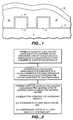
- FIG. 1is a fragmentary vertical cross-sectional view of an integrated circuit shown formed with a layer of tensile stressed low k dielectric material formed thereon with a capping layer of compressively stressed non-low k dielectric material formed over the low k layer.
- FIG. 2is a flowsheet illustrating the process of the invention.
- the inventioncomprises a process which inhibits cracking of a layer of low k silicon oxide dielectric material on an integrated circuit during subsequent processing of the layer of low k silicon oxide dielectric material.
- the processcomprises: forming a layer of low k silicon oxide dielectric material on an integrated circuit structure on a semiconductor substrate; and forming over the layer of low k silicon oxide dielectric material a capping layer of dielectric material having: a dielectric constant not exceeding about 4; a thickness of at least about 300 nm; and a compressive stress of at least about 3 ⁇ 10 9 dynes/cm 2 .
- an integrated circuit structure formed on a silicon semiconductor substrateis generally indicated at 2.
- the upper surface of integrated circuit structure 2may comprise exposed silicon portions and/or metal surfaces such as, for example, a lower level of metal interconnects, as shown by raised spaced apart metal lines 6 .
- a lower barrier layer 10may be formed over integrated circuit structure 2 .
- Lower barrier layer 10which may also facilitate adhesion of the integrated circuit structure and the layer of low k dielectric material to be formed thereon, may comprise a conventional (non-low k) PECVD silicon oxide layer deposited on integrated circuit structure 2 to a thickness of about 50 nm.
- the presence of lower barrier layer 10will serve to protect the underlying integrated circuit structure 2 , including metal lines 6 , from moisture and other reaction residues which will be released during the curing of the layer of low k dielectric material to be formed over lower barrier layer 10 .
- layer 20 of low k silicon oxide dielectric materialOver lower barrier layer 10 is then formed layer 20 of low k silicon oxide dielectric material.
- low kis intended to define a dielectric constant of a dielectric material of 3.5 or less.
- the dielectric constant of a “low k” materialwill be 3.0 or less.
- Layer 20 of low k silicon oxide dielectric materialmay be deposited over lower barrier layer 10 by reacting hydrogen peroxide with a carbon-substituted silane such as methyl silane, as described in the aforementioned article by L. Peters, and described in general for silane and peroxide reactions in Dobson U.S. Pat. No. 5,874,367, the subject matter of which is hereby incorporated by reference.
- the void-free low k silicon oxide dielectric materialmay also be deposited by reacting a mild oxidant such as hydrogen peroxide with the carbon-substituted silane materials disclosed in Aronowitz et al. Serial No. 09/274,457, filed on Mar. 22, 1999, and assigned to the assignee of this application, the subject matter of which is also hereby incorporated by reference.
- the process of the inventionmay also be useful with any other low k dielectric material having a high tensile stress, but will be described herein with respect to a high tensile stress low k carbon-substituted silicon oxide dielectric material by way of illustration and not of limitation.
- the thickness of layer 20 of low k carbon-substituted silicon oxide dielectric materialwill vary with the application. In one embodiment, for example, the thickness of layer 20 may equal that of the height of the underlying metal lines to ensure that the horizontal space between adjacent lines is filled with low k dielectric material to reduce the horizontal capacitance between adjacent metal lines.
- the thickness of layer 20 of low k carbon-substituted silicon oxide dielectric materialmay vary from 300 nm to about 700 nm, but typically will be about 600 nm.
- a compressively stressed silicon oxide capping layer 30is then formed over layer 20 of low k carbon-substituted silicon oxide dielectric material to compensate for the tensile stress of low k layer 20 , as well as provide a moisture barrier for the upper surface of low k layer 20 .
- Capping layer 30preferably comprises a silicon oxide layer having a dielectric constant not exceeding about 4; a thickness of at least about 300 nm, and typically ranging from about 300 nm to about 400 nm; and a compressive stress of at least about 3 ⁇ 10 9 dynes/cm 2 , and typically ranging from about 3 ⁇ 10 9 dynes/cm 2 to about 4 ⁇ 10 9 dynes/cm 2 .
- the minimum thickness of at least about 300 nmis needed to provide a capping layer having sufficient compressive stress to compensate for the tensile stress of the underlying low k dielectric layer and will be sufficient to prevent diffusion of moisture through capping layer 30 to low k layer 20 .
- the maximum thickness of about 400 nmrelates to the higher dielectric constant of the capping layer and the desire to keep the combined dielectric constant of the composite of dielectric layers (lower barrier layer, low k layer, and capping layer) as low as possible.
- Other dielectric materialsuch as silicon nitride may be substituted for silicon oxide as the capping layer provided that they meet the about criteria regarding dielectric constant, thicknesses, and compressive stress.
- capping layer 30may be formed by the reaction of silane and N 2 O in a plasma enhanced chemical vapor deposition (PECVD) reaction carried out in a vacuum chamber maintained at a pressure of from about 600 milliTorr to about 1000 milliTorr, preferably from about 700 milliTorr to about 900 milliTorr, and typically about 800 milliTorr; and a temperature ranging from about 300° C. to about 400° C., preferably from about 325° C. to about 375° C., and typically about 350° C.
- the plasma power, during the reaction to form capping layer 30 of silicon oxideis maintained at a level of from about 250 watts to about 350 watts, preferably from about 275 watts to about 325 watts, and typically at about 300 watts.
- PECVDplasma enhanced chemical vapor deposition
- the reactionmay be carried out by flowing the reactants into a PECVD chamber at a rate equivalent to flowing the reactants into a 10 liter chamber, containing a 200 mm diameter substrate, of from about 35 standard cubic centimeters per minute (sccm) to about 45 sccm silane, typically about 40 sccm; and N 2 O at a rate of from about 3800 sccm to about 4200 sccm typically about 4000 sccm.
- the plasmais ignited and then maintained within the power range once flow of the reactants has commenced.
- the flow of reactants and the plasmaare maintained in the reactor until the desired thickness of the deposit has been achieved, after which the flow is shut off and the plasma is extinguished.
- the above reactionwill be carried out for from about 80 to about 90 seconds.
- the actual flow rates and reaction times to achieve the desired thickness of silicon oxide capping layerwill depend on chamber size and wafer diameter.
- capping layer 30is formed over low k dielectric layer 20 without exposing the surface of low k dielectric layer 20 to the atmosphere.
- the process steps of depositing low k dielectric layer 20 and capping layer 30are carried out in the same apparatus, for example, by forming low k dielectric layer 20 in a chamber specifically designed to deposit low k dielectric material such as, for example, low k carbon-substituted silicon oxide dielectric material.
- the substrateis moved, under vacuum, to a second chamber, such as a PECVD chamber or a HDP chamber where capping layer 30 is formed over low. k layer 20 .
- a second chambersuch as a PECVD chamber or a HDP chamber
- capping layer 30is formed over low. k layer 20 .
- Such a multiple chamber apparatussometimes also known as a cluster tool, is commercially available from various sources such as the Applied Materials Producer, the Trikon Technology fxp, or the Novellus Concept Two Sequel.
- Three 200 mm diameter silicon wafer substrates having identical integrated circuit structures formed thereoncan be placed (consecutively—not together) in a 10 liter PECVD chamber of a multiple chamber vacuum apparatus maintained at a pressure of 1400 milliTorr and a temperature of ⁇ 350° C. Silane is flowed into the chamber at a rate of 150 sccm and N 2 O is flowed into the chamber at 3500 sccm.
- a plasmais ignited in the chamber and maintained at a power level of about 100 watts for the deposition time of 13 seconds, after which the plasma would be extinguished and the flow of reactant gases shut off, resulting in the deposition of about 50 nm of a lower barrier layer of silicon oxide over the integrated circuit structure previously formed over each of the silicon wafers.
- the three identically coated wafersare then each transferred (separately) under vacuum to a 10 liter CVD chamber in the same apparatus where a 300 nm layer of low k silicon oxide dielectric material can be deposited over the lower barrier layer by flowing 70 sccm of methyl silane gas and 0.75 grams/minute of hydrogen peroxide vapor into the chamber for 40 seconds while maintaining a pressure of 900 milliTorr and a temperature of 5° C. in the chamber. The flow of reactants is then shut off. Without exposing the exposed low k surfaces to the atmosphere, two of the coated wafers are then transferred back to the PECVD chamber for formation of a capping layer thereon.
- the PECVD chamber of the multiple chamber vacuum apparatusis maintained at a pressure of 800 milliTorr and a temperature of ⁇ 350° C. during the formation of the silicon oxide capping layer over the low k dielectric layer on the two wafers.
- Silaneis flowed into the chamber at a rate of about 40 sccm and N 2 O is flowed into the chamber at about 4000 sccm.
- a plasmais ignited in the chamber and maintained at a power level of about 300 watts for the entire deposition.
- One of the wafersis subjected to these deposition conditions for about 15 seconds, while the deposition time for the other wafer is about 84 seconds, after which (for each of the two wafers) the plasma would be extinguished and the flow of reactant gases shut off.
- the thickness of the capping layer on the wafer having a 15 second deposit timewill measure about 50 nm, wile the thickness of the capping layer having the 84 second deposit time will measure about 300 nm.
- Each of the three waferscan then be placed in an annealing furnace at a temperature of about 400° C. for a period of about 3 minutes. Each wafer is then removed, cooled to ambient temperature, and examined under a 200X microscope for cracking of the low k dielectric layer. Both the wafer without the capping layer and the wafer with the 50 nm capping layer will be found to have cracked during the high temperature anneal, while the wafer having the 300 nm capping layer will not exhibit cracking of the low k dielectric layer. If the tensile stress of the 300 nm thick capping layer is measured, it will be found to range between ⁇ 3-4 ⁇ 10 9 dynes/cm 2 . If the dielectric constant (k) of the capping layer is also measured, it will be found to be about 4.
- the process of the inventionresults in the prevention of cracking in a low k dielectric layer during annealing at an elevated temperature, without an unacceptable increase in the dielectric constant of the composite layer, by the formation, over the low k dielectric layer, of a capping layer such as silicon oxide having a thickness of at least about 300 nm, a dielectric constant not exceeding about 4, and a compressive stress of at least about 3 ⁇ 10 9 dynes/cm 2 .
- a capping layersuch as silicon oxide having a thickness of at least about 300 nm, a dielectric constant not exceeding about 4
- a compressive stressof at least about 3 ⁇ 10 9 dynes/cm 2 .
Landscapes
- Engineering & Computer Science (AREA)
- Physics & Mathematics (AREA)
- Condensed Matter Physics & Semiconductors (AREA)
- General Physics & Mathematics (AREA)
- Manufacturing & Machinery (AREA)
- Computer Hardware Design (AREA)
- Microelectronics & Electronic Packaging (AREA)
- Power Engineering (AREA)
- Chemical & Material Sciences (AREA)
- Chemical Kinetics & Catalysis (AREA)
- Formation Of Insulating Films (AREA)
- Internal Circuitry In Semiconductor Integrated Circuit Devices (AREA)
Abstract
Description
Claims (21)
Priority Applications (1)
| Application Number | Priority Date | Filing Date | Title |
|---|---|---|---|
| US09/704,635US6420277B1 (en) | 2000-11-01 | 2000-11-01 | Process for inhibiting crack formation in low dielectric constant dielectric films of integrated circuit structure |
Applications Claiming Priority (1)
| Application Number | Priority Date | Filing Date | Title |
|---|---|---|---|
| US09/704,635US6420277B1 (en) | 2000-11-01 | 2000-11-01 | Process for inhibiting crack formation in low dielectric constant dielectric films of integrated circuit structure |
Publications (1)
| Publication Number | Publication Date |
|---|---|
| US6420277B1true US6420277B1 (en) | 2002-07-16 |
Family
ID=24830303
Family Applications (1)
| Application Number | Title | Priority Date | Filing Date |
|---|---|---|---|
| US09/704,635Expired - LifetimeUS6420277B1 (en) | 2000-11-01 | 2000-11-01 | Process for inhibiting crack formation in low dielectric constant dielectric films of integrated circuit structure |
Country Status (1)
| Country | Link |
|---|---|
| US (1) | US6420277B1 (en) |
Cited By (5)
| Publication number | Priority date | Publication date | Assignee | Title |
|---|---|---|---|---|
| US6632478B2 (en)* | 2001-02-22 | 2003-10-14 | Applied Materials, Inc. | Process for forming a low dielectric constant carbon-containing film |
| DE10250364A1 (en)* | 2002-10-29 | 2004-05-19 | Infineon Technologies Ag | Filling irregularities and intermediate cavities during surface structuring on semiconductor, employs flow-fill process using filler of low dielectric constant |
| US20060039428A1 (en)* | 2004-08-17 | 2006-02-23 | Sharp Kabushiki Kaisha | Semiconductor laser device and manufacturing method therefor |
| US20110204491A1 (en)* | 2007-08-06 | 2011-08-25 | Chin-Hsiang Lin | Dielectric layer structure |
| US8937011B2 (en) | 2012-12-18 | 2015-01-20 | Sandisk 3D Llc | Method of forming crack free gap fill |
Citations (47)
| Publication number | Priority date | Publication date | Assignee | Title |
|---|---|---|---|---|
| US3012861A (en) | 1960-01-15 | 1961-12-12 | Du Pont | Production of silicon |
| US3178392A (en) | 1962-04-09 | 1965-04-13 | Rohm & Haas | Heterocyclic and linear siliconmethylene and polysiloxane compounds containing siliconmethylene units and their preparation |
| US3652331A (en) | 1968-03-22 | 1972-03-28 | Shumpei Yamazaki | Process for forming a film on the surface of a substrate by a gas phase |
| US3832202A (en) | 1972-08-08 | 1974-08-27 | Motorola Inc | Liquid silica source for semiconductors liquid silica source for semiconductors |
| US3920865A (en) | 1969-03-29 | 1975-11-18 | Degussa | Process of hydrophorizing highly dispersed metal or metalloid oxides |
| US4705725A (en) | 1986-11-28 | 1987-11-10 | E. I. Du Pont De Nemours And Company | Substrates with sterically-protected, stable, covalently-bonded organo-silane films |
| JPS633437A (en) | 1986-06-23 | 1988-01-08 | Sony Corp | Manufacture of semiconductor device |
| US4771328A (en) | 1983-10-13 | 1988-09-13 | International Business Machine Corporation | Semiconductor device and process |
| US5194333A (en) | 1989-12-18 | 1993-03-16 | Tosoh Corporation | Packing material for reversed phase chromatography and process for its preparation |
| US5314845A (en) | 1989-09-28 | 1994-05-24 | Applied Materials, Inc. | Two step process for forming void-free oxide layer over stepped surface of semiconductor wafer |
| US5364800A (en) | 1993-06-24 | 1994-11-15 | Texas Instruments Incorporated | Varying the thickness of the surface silicon layer in a silicon-on-insulator substrate |
| US5376595A (en) | 1992-08-28 | 1994-12-27 | Allied-Signal Inc. | Silicon carboxide ceramics from spirosiloxanes |
| US5470801A (en) | 1993-06-28 | 1995-11-28 | Lsi Logic Corporation | Low dielectric constant insulation layer for integrated circuit structure and method of making same |
| EP0706216A2 (en) | 1994-10-03 | 1996-04-10 | Sony Corporation | Interlayer dielectric structure for semiconductor device |
| US5559367A (en) | 1994-07-12 | 1996-09-24 | International Business Machines Corporation | Diamond-like carbon for use in VLSI and ULSI interconnect systems |
| US5558718A (en) | 1994-04-08 | 1996-09-24 | The Regents, University Of California | Pulsed source ion implantation apparatus and method |
| US5580429A (en) | 1992-08-25 | 1996-12-03 | Northeastern University | Method for the deposition and modification of thin films using a combination of vacuum arcs and plasma immersion ion implantation |
| US5628871A (en) | 1993-09-17 | 1997-05-13 | Fujitsu Limited | Method of removing resist mask and a method of manufacturing semiconductor device |
| US5675187A (en) | 1994-07-15 | 1997-10-07 | Texas Instruments Incorporated | Reliability of metal leads in high speed LSI semiconductors using dummy vias |
| US5688724A (en) | 1992-07-02 | 1997-11-18 | National Semiconductor Corporation | Method of providing a dielectric structure for semiconductor devices |
| US5847461A (en)* | 1995-05-05 | 1998-12-08 | Applied Materials, Inc. | Integrated circuit structure having contact openings and vias filled by self-extrusion of overlying metal layer |
| DE19804375A1 (en) | 1997-06-26 | 1999-01-07 | Mitsubishi Electric Corp | Semiconductor device with interlayer insulating film |
| US5858879A (en) | 1997-06-06 | 1999-01-12 | Taiwan Semiconductor Manufacturing Co., Ltd. | Method for etching metal lines with enhanced profile control |
| US5874367A (en) | 1992-07-04 | 1999-02-23 | Trikon Technologies Limited | Method of treating a semi-conductor wafer |
| US5874745A (en) | 1997-08-05 | 1999-02-23 | International Business Machines Corporation | Thin film transistor with carbonaceous gate dielectric |
| US5882489A (en) | 1996-04-26 | 1999-03-16 | Ulvac Technologies, Inc. | Processes for cleaning and stripping photoresist from surfaces of semiconductor wafers |
| US5904154A (en) | 1997-07-24 | 1999-05-18 | Vanguard International Semiconductor Corporation | Method for removing fluorinated photoresist layers from semiconductor substrates |
| US5915203A (en) | 1997-06-10 | 1999-06-22 | Vlsi Technology, Inc. | Method for producing deep submicron interconnect vias |
| US5939763A (en) | 1996-09-05 | 1999-08-17 | Advanced Micro Devices, Inc. | Ultrathin oxynitride structure and process for VLSI applications |
| WO1999041423A2 (en) | 1998-02-11 | 1999-08-19 | Applied Materials, Inc. | Plasma processes for depositing low dielectric constant films |
| EP0949663A2 (en) | 1998-04-08 | 1999-10-13 | Nec Corporation | Deposition of an insulating film comprising carbon |
| US6025263A (en) | 1997-07-15 | 2000-02-15 | Nanya Technology Corporation | Underlayer process for high O3 /TEOS interlayer dielectric deposition |
| US6028015A (en) | 1999-03-29 | 2000-02-22 | Lsi Logic Corporation | Process for treating damaged surfaces of low dielectric constant organo silicon oxide insulation material to inhibit moisture absorption |
| US6037248A (en) | 1997-06-13 | 2000-03-14 | Micron Technology, Inc. | Method of fabricating integrated circuit wiring with low RC time delay |
| US6043167A (en) | 1996-10-11 | 2000-03-28 | Lg Semicon Co., Ltd. | Method for forming low dielectric constant insulating film |
| US6051477A (en) | 1995-11-01 | 2000-04-18 | Hyundai Electronics Industries Co., Ltd. | Method of fabricating semiconductor device |
| US6051073A (en) | 1998-02-11 | 2000-04-18 | Silicon Genesis Corporation | Perforated shield for plasma immersion ion implantation |
| US6066574A (en) | 1998-11-06 | 2000-05-23 | Advanced Micro Devices, Inc. | Hot plate cure process for BCB low k interlevel dielectric |
| US6114259A (en) | 1999-07-27 | 2000-09-05 | Lsi Logic Corporation | Process for treating exposed surfaces of a low dielectric constant carbon doped silicon oxide dielectric material to protect the material from damage |
| JP2000267128A (en) | 1999-03-17 | 2000-09-29 | Semiconductor Energy Lab Co Ltd | Semiconductor device |
| US6147012A (en)* | 1999-11-12 | 2000-11-14 | Lsi Logic Corporation | Process for forming low k silicon oxide dielectric material while suppressing pressure spiking and inhibiting increase in dielectric constant |
| US6153524A (en) | 1997-07-29 | 2000-11-28 | Silicon Genesis Corporation | Cluster tool method using plasma immersion ion implantation |
| US6177302B1 (en)* | 1990-11-09 | 2001-01-23 | Semiconductor Energy Laboratory Co., Ltd. | Method of manufacturing a thin film transistor using multiple sputtering chambers |
| US6204192B1 (en) | 1999-03-29 | 2001-03-20 | Lsi Logic Corporation | Plasma cleaning process for openings formed in at least one low dielectric constant insulation layer over copper metallization in integrated circuit structures |
| US6232658B1 (en) | 1999-06-30 | 2001-05-15 | Lsi Logic Corporation | Process to prevent stress cracking of dielectric films on semiconductor wafers |
| US6245666B1 (en)* | 2000-04-03 | 2001-06-12 | Taiwan Semiconductor Manufacturing Company | Method for forming a delamination resistant multi-layer dielectric layer for passivating a conductor layer |
| US6316354B1 (en)* | 1999-10-26 | 2001-11-13 | Lsi Logic Corporation | Process for removing resist mask of integrated circuit structure which mitigates damage to underlying low dielectric constant silicon oxide dielectric layer |
- 2000
- 2000-11-01USUS09/704,635patent/US6420277B1/ennot_activeExpired - Lifetime
Patent Citations (48)
| Publication number | Priority date | Publication date | Assignee | Title |
|---|---|---|---|---|
| US3012861A (en) | 1960-01-15 | 1961-12-12 | Du Pont | Production of silicon |
| US3178392A (en) | 1962-04-09 | 1965-04-13 | Rohm & Haas | Heterocyclic and linear siliconmethylene and polysiloxane compounds containing siliconmethylene units and their preparation |
| US3652331A (en) | 1968-03-22 | 1972-03-28 | Shumpei Yamazaki | Process for forming a film on the surface of a substrate by a gas phase |
| US3920865A (en) | 1969-03-29 | 1975-11-18 | Degussa | Process of hydrophorizing highly dispersed metal or metalloid oxides |
| US3832202A (en) | 1972-08-08 | 1974-08-27 | Motorola Inc | Liquid silica source for semiconductors liquid silica source for semiconductors |
| US4771328A (en) | 1983-10-13 | 1988-09-13 | International Business Machine Corporation | Semiconductor device and process |
| JPS633437A (en) | 1986-06-23 | 1988-01-08 | Sony Corp | Manufacture of semiconductor device |
| US4705725A (en) | 1986-11-28 | 1987-11-10 | E. I. Du Pont De Nemours And Company | Substrates with sterically-protected, stable, covalently-bonded organo-silane films |
| US5314845A (en) | 1989-09-28 | 1994-05-24 | Applied Materials, Inc. | Two step process for forming void-free oxide layer over stepped surface of semiconductor wafer |
| US5194333A (en) | 1989-12-18 | 1993-03-16 | Tosoh Corporation | Packing material for reversed phase chromatography and process for its preparation |
| US6177302B1 (en)* | 1990-11-09 | 2001-01-23 | Semiconductor Energy Laboratory Co., Ltd. | Method of manufacturing a thin film transistor using multiple sputtering chambers |
| US5688724A (en) | 1992-07-02 | 1997-11-18 | National Semiconductor Corporation | Method of providing a dielectric structure for semiconductor devices |
| US5874367A (en) | 1992-07-04 | 1999-02-23 | Trikon Technologies Limited | Method of treating a semi-conductor wafer |
| US5580429A (en) | 1992-08-25 | 1996-12-03 | Northeastern University | Method for the deposition and modification of thin films using a combination of vacuum arcs and plasma immersion ion implantation |
| US5376595A (en) | 1992-08-28 | 1994-12-27 | Allied-Signal Inc. | Silicon carboxide ceramics from spirosiloxanes |
| US5364800A (en) | 1993-06-24 | 1994-11-15 | Texas Instruments Incorporated | Varying the thickness of the surface silicon layer in a silicon-on-insulator substrate |
| US5470801A (en) | 1993-06-28 | 1995-11-28 | Lsi Logic Corporation | Low dielectric constant insulation layer for integrated circuit structure and method of making same |
| US5864172A (en) | 1993-06-28 | 1999-01-26 | Lsi Logic Corporation | Low dielectric constant insulation layer for integrated circuit structure and method of making same |
| US5628871A (en) | 1993-09-17 | 1997-05-13 | Fujitsu Limited | Method of removing resist mask and a method of manufacturing semiconductor device |
| US5558718A (en) | 1994-04-08 | 1996-09-24 | The Regents, University Of California | Pulsed source ion implantation apparatus and method |
| US5559367A (en) | 1994-07-12 | 1996-09-24 | International Business Machines Corporation | Diamond-like carbon for use in VLSI and ULSI interconnect systems |
| US5675187A (en) | 1994-07-15 | 1997-10-07 | Texas Instruments Incorporated | Reliability of metal leads in high speed LSI semiconductors using dummy vias |
| EP0706216A2 (en) | 1994-10-03 | 1996-04-10 | Sony Corporation | Interlayer dielectric structure for semiconductor device |
| US5847461A (en)* | 1995-05-05 | 1998-12-08 | Applied Materials, Inc. | Integrated circuit structure having contact openings and vias filled by self-extrusion of overlying metal layer |
| US6051477A (en) | 1995-11-01 | 2000-04-18 | Hyundai Electronics Industries Co., Ltd. | Method of fabricating semiconductor device |
| US5882489A (en) | 1996-04-26 | 1999-03-16 | Ulvac Technologies, Inc. | Processes for cleaning and stripping photoresist from surfaces of semiconductor wafers |
| US5939763A (en) | 1996-09-05 | 1999-08-17 | Advanced Micro Devices, Inc. | Ultrathin oxynitride structure and process for VLSI applications |
| US6043167A (en) | 1996-10-11 | 2000-03-28 | Lg Semicon Co., Ltd. | Method for forming low dielectric constant insulating film |
| US5858879A (en) | 1997-06-06 | 1999-01-12 | Taiwan Semiconductor Manufacturing Co., Ltd. | Method for etching metal lines with enhanced profile control |
| US5915203A (en) | 1997-06-10 | 1999-06-22 | Vlsi Technology, Inc. | Method for producing deep submicron interconnect vias |
| US6037248A (en) | 1997-06-13 | 2000-03-14 | Micron Technology, Inc. | Method of fabricating integrated circuit wiring with low RC time delay |
| DE19804375A1 (en) | 1997-06-26 | 1999-01-07 | Mitsubishi Electric Corp | Semiconductor device with interlayer insulating film |
| US6025263A (en) | 1997-07-15 | 2000-02-15 | Nanya Technology Corporation | Underlayer process for high O3 /TEOS interlayer dielectric deposition |
| US5904154A (en) | 1997-07-24 | 1999-05-18 | Vanguard International Semiconductor Corporation | Method for removing fluorinated photoresist layers from semiconductor substrates |
| US6153524A (en) | 1997-07-29 | 2000-11-28 | Silicon Genesis Corporation | Cluster tool method using plasma immersion ion implantation |
| US5874745A (en) | 1997-08-05 | 1999-02-23 | International Business Machines Corporation | Thin film transistor with carbonaceous gate dielectric |
| WO1999041423A2 (en) | 1998-02-11 | 1999-08-19 | Applied Materials, Inc. | Plasma processes for depositing low dielectric constant films |
| US6051073A (en) | 1998-02-11 | 2000-04-18 | Silicon Genesis Corporation | Perforated shield for plasma immersion ion implantation |
| EP0949663A2 (en) | 1998-04-08 | 1999-10-13 | Nec Corporation | Deposition of an insulating film comprising carbon |
| US6066574A (en) | 1998-11-06 | 2000-05-23 | Advanced Micro Devices, Inc. | Hot plate cure process for BCB low k interlevel dielectric |
| JP2000267128A (en) | 1999-03-17 | 2000-09-29 | Semiconductor Energy Lab Co Ltd | Semiconductor device |
| US6028015A (en) | 1999-03-29 | 2000-02-22 | Lsi Logic Corporation | Process for treating damaged surfaces of low dielectric constant organo silicon oxide insulation material to inhibit moisture absorption |
| US6204192B1 (en) | 1999-03-29 | 2001-03-20 | Lsi Logic Corporation | Plasma cleaning process for openings formed in at least one low dielectric constant insulation layer over copper metallization in integrated circuit structures |
| US6232658B1 (en) | 1999-06-30 | 2001-05-15 | Lsi Logic Corporation | Process to prevent stress cracking of dielectric films on semiconductor wafers |
| US6114259A (en) | 1999-07-27 | 2000-09-05 | Lsi Logic Corporation | Process for treating exposed surfaces of a low dielectric constant carbon doped silicon oxide dielectric material to protect the material from damage |
| US6316354B1 (en)* | 1999-10-26 | 2001-11-13 | Lsi Logic Corporation | Process for removing resist mask of integrated circuit structure which mitigates damage to underlying low dielectric constant silicon oxide dielectric layer |
| US6147012A (en)* | 1999-11-12 | 2000-11-14 | Lsi Logic Corporation | Process for forming low k silicon oxide dielectric material while suppressing pressure spiking and inhibiting increase in dielectric constant |
| US6245666B1 (en)* | 2000-04-03 | 2001-06-12 | Taiwan Semiconductor Manufacturing Company | Method for forming a delamination resistant multi-layer dielectric layer for passivating a conductor layer |
Non-Patent Citations (8)
| Title |
|---|
| Bothra, S., et al., "Integration of 0.25 mum Three and Five Level Interconnect Sytem for High Performance ASIC", 1997 Proceedings Fourteenth International VMIC Conference, Santa Clara, CA, Jun. 10-12, 1997, pp. 43-48. |
| Bothra, S., et al., "Integration of 0.25 μm Three and Five Level Interconnect Sytem for High Performance ASIC", 1997 Proceedings Fourteenth International VMIC Conference, Santa Clara, CA, Jun. 10-12, 1997, pp. 43-48. |
| Dobson, C.D., et al., "Advanced SiO2 Planarization Using Silane and H2O2", Semiconductor International, Dec. 1994, pp. 85-88. |
| Koda, Seiichiro, et al., "A Study of Inhibition Effects for Silane Combusion by Additive Gases", Combustion and Flame, vol. 73, No. 2, Aug., 1988, pp. 187-194. |
| McClatchie, S., et al., "Low Dielectric Constant Oxide Films Deposited Using CVD Techniques", 1998 Proceedings Fourth International DUMIC Conference, Feb. 16-17, 1998, pp. 311-318. |
| Peters, Laura, "Low-k Dielectrics: Will Spin-On or CVD Prevail?", Semiconductor International, vol. 23, No. 6, Jun., 2000, pp. 108-110, 114, 116, 118, 122, and 124. |
| Peters, Laura, "Pursuing the Perfect Low-k Dielectric", Semiconductor International, vol. 21, No. 10, Sep., 1998, pp. 64-66, 68, 70, 72, and 74. |
| Sugahara, Satoshi, et al., "Chemical Vapor Deposition of CF3-Incorporated Silica Films for Interlayer Dielectric Application", 1999 Joint International Meeting, Electrochemical Society Meeting Abstracts, vol. 99-2, 1999, Abstract No. 746. |
Cited By (5)
| Publication number | Priority date | Publication date | Assignee | Title |
|---|---|---|---|---|
| US6632478B2 (en)* | 2001-02-22 | 2003-10-14 | Applied Materials, Inc. | Process for forming a low dielectric constant carbon-containing film |
| DE10250364A1 (en)* | 2002-10-29 | 2004-05-19 | Infineon Technologies Ag | Filling irregularities and intermediate cavities during surface structuring on semiconductor, employs flow-fill process using filler of low dielectric constant |
| US20060039428A1 (en)* | 2004-08-17 | 2006-02-23 | Sharp Kabushiki Kaisha | Semiconductor laser device and manufacturing method therefor |
| US20110204491A1 (en)* | 2007-08-06 | 2011-08-25 | Chin-Hsiang Lin | Dielectric layer structure |
| US8937011B2 (en) | 2012-12-18 | 2015-01-20 | Sandisk 3D Llc | Method of forming crack free gap fill |
Similar Documents
| Publication | Publication Date | Title |
|---|---|---|
| US6852647B2 (en) | Removable amorphous carbon CMP stop | |
| KR100696033B1 (en) | Semiconductor substrate processing method | |
| US6632478B2 (en) | Process for forming a low dielectric constant carbon-containing film | |
| US7226876B2 (en) | Method of modifying interlayer adhesion | |
| US5800877A (en) | Method for forming a fluorine containing silicon oxide film | |
| US6440878B1 (en) | Method to enhance the adhesion of silicon nitride to low-k fluorinated amorphous carbon using a silicon carbide adhesion promoter layer | |
| KR100743775B1 (en) | Method and apparatus for treating l0w k dielectric layers to reduce diffusion | |
| US7354852B2 (en) | Method of forming interconnection in semiconductor device | |
| US8137764B2 (en) | Mechanical enhancer additives for low dielectric films | |
| US7851384B2 (en) | Method to mitigate impact of UV and E-beam exposure on semiconductor device film properties by use of a bilayer film | |
| US7825040B1 (en) | Method for depositing flowable material using alkoxysilane or aminosilane precursor | |
| US8173537B1 (en) | Methods for reducing UV and dielectric diffusion barrier interaction | |
| JP3409984B2 (en) | Semiconductor device and method of manufacturing semiconductor device | |
| JP4068072B2 (en) | Semiconductor device and manufacturing method thereof | |
| JPH08153784A (en) | Method for manufacturing semiconductor device | |
| US20090054674A1 (en) | Mechanical Enhancement of Dense and Porous Organosilicate Materials by UV Exposure | |
| WO1998008249A1 (en) | Method and apparatus for depositing a planarized dielectric layer on a semiconductor substrate | |
| JP2003045959A (en) | Semiconductor device and method of manufacturing the same | |
| US6420277B1 (en) | Process for inhibiting crack formation in low dielectric constant dielectric films of integrated circuit structure | |
| Robles et al. | Moisture resistance of plasma enhanced chemical vapor deposited oxides used for ultralarge scale integrated device applications | |
| KR20050083787A (en) | Semiconductor device and process for producing the same | |
| US6559048B1 (en) | Method of making a sloped sidewall via for integrated circuit structure to suppress via poisoning | |
| JP2011082308A (en) | Method of manufacturing semiconductor apparatus | |
| US8003549B1 (en) | Methods of forming moisture barrier for low K film integration with anti-reflective layers | |
| KR20000076713A (en) | Method for forming an interlayer insulating film, and semiconductor devices |
Legal Events
| Date | Code | Title | Description |
|---|---|---|---|
| AS | Assignment | Owner name:LSI LOGIC CORPORATION, CALIFORNIA Free format text:ASSIGNMENT OF ASSIGNORS INTEREST;ASSIGNORS:CATABAY, WILBUR G.;HSIA, WEI-JEN;LU, HONG QIANG;REEL/FRAME:011270/0406;SIGNING DATES FROM 20001030 TO 20001031 | |
| STCF | Information on status: patent grant | Free format text:PATENTED CASE | |
| CC | Certificate of correction | ||
| FPAY | Fee payment | Year of fee payment:4 | |
| FEPP | Fee payment procedure | Free format text:PAYOR NUMBER ASSIGNED (ORIGINAL EVENT CODE: ASPN); ENTITY STATUS OF PATENT OWNER: LARGE ENTITY | |
| FPAY | Fee payment | Year of fee payment:8 | |
| FPAY | Fee payment | Year of fee payment:12 | |
| AS | Assignment | Owner name:DEUTSCHE BANK AG NEW YORK BRANCH, AS COLLATERAL AG Free format text:PATENT SECURITY AGREEMENT;ASSIGNORS:LSI CORPORATION;AGERE SYSTEMS LLC;REEL/FRAME:032856/0031 Effective date:20140506 | |
| AS | Assignment | Owner name:LSI CORPORATION, CALIFORNIA Free format text:CHANGE OF NAME;ASSIGNOR:LSI LOGIC CORPORATION;REEL/FRAME:033102/0270 Effective date:20070406 | |
| AS | Assignment | Owner name:AVAGO TECHNOLOGIES GENERAL IP (SINGAPORE) PTE. LTD Free format text:ASSIGNMENT OF ASSIGNORS INTEREST;ASSIGNOR:LSI CORPORATION;REEL/FRAME:035390/0388 Effective date:20140814 | |
| AS | Assignment | Owner name:LSI CORPORATION, CALIFORNIA Free format text:TERMINATION AND RELEASE OF SECURITY INTEREST IN PATENT RIGHTS (RELEASES RF 032856-0031);ASSIGNOR:DEUTSCHE BANK AG NEW YORK BRANCH, AS COLLATERAL AGENT;REEL/FRAME:037684/0039 Effective date:20160201 Owner name:AGERE SYSTEMS LLC, PENNSYLVANIA Free format text:TERMINATION AND RELEASE OF SECURITY INTEREST IN PATENT RIGHTS (RELEASES RF 032856-0031);ASSIGNOR:DEUTSCHE BANK AG NEW YORK BRANCH, AS COLLATERAL AGENT;REEL/FRAME:037684/0039 Effective date:20160201 | |
| AS | Assignment | Owner name:BANK OF AMERICA, N.A., AS COLLATERAL AGENT, NORTH CAROLINA Free format text:PATENT SECURITY AGREEMENT;ASSIGNOR:AVAGO TECHNOLOGIES GENERAL IP (SINGAPORE) PTE. LTD.;REEL/FRAME:037808/0001 Effective date:20160201 Owner name:BANK OF AMERICA, N.A., AS COLLATERAL AGENT, NORTH Free format text:PATENT SECURITY AGREEMENT;ASSIGNOR:AVAGO TECHNOLOGIES GENERAL IP (SINGAPORE) PTE. LTD.;REEL/FRAME:037808/0001 Effective date:20160201 | |
| AS | Assignment | Owner name:AVAGO TECHNOLOGIES GENERAL IP (SINGAPORE) PTE. LTD., SINGAPORE Free format text:TERMINATION AND RELEASE OF SECURITY INTEREST IN PATENTS;ASSIGNOR:BANK OF AMERICA, N.A., AS COLLATERAL AGENT;REEL/FRAME:041710/0001 Effective date:20170119 Owner name:AVAGO TECHNOLOGIES GENERAL IP (SINGAPORE) PTE. LTD Free format text:TERMINATION AND RELEASE OF SECURITY INTEREST IN PATENTS;ASSIGNOR:BANK OF AMERICA, N.A., AS COLLATERAL AGENT;REEL/FRAME:041710/0001 Effective date:20170119 | |
| AS | Assignment | Owner name:BELL SEMICONDUCTOR, LLC, ILLINOIS Free format text:ASSIGNMENT OF ASSIGNORS INTEREST;ASSIGNORS:AVAGO TECHNOLOGIES GENERAL IP (SINGAPORE) PTE. LTD.;BROADCOM CORPORATION;REEL/FRAME:044886/0608 Effective date:20171208 | |
| AS | Assignment | Owner name:CORTLAND CAPITAL MARKET SERVICES LLC, AS COLLATERA Free format text:SECURITY INTEREST;ASSIGNORS:HILCO PATENT ACQUISITION 56, LLC;BELL SEMICONDUCTOR, LLC;BELL NORTHERN RESEARCH, LLC;REEL/FRAME:045216/0020 Effective date:20180124 | |
| AS | Assignment | Owner name:BELL NORTHERN RESEARCH, LLC, ILLINOIS Free format text:RELEASE BY SECURED PARTY;ASSIGNOR:CORTLAND CAPITAL MARKET SERVICES LLC;REEL/FRAME:059720/0719 Effective date:20220401 Owner name:BELL SEMICONDUCTOR, LLC, ILLINOIS Free format text:RELEASE BY SECURED PARTY;ASSIGNOR:CORTLAND CAPITAL MARKET SERVICES LLC;REEL/FRAME:059720/0719 Effective date:20220401 Owner name:HILCO PATENT ACQUISITION 56, LLC, ILLINOIS Free format text:RELEASE BY SECURED PARTY;ASSIGNOR:CORTLAND CAPITAL MARKET SERVICES LLC;REEL/FRAME:059720/0719 Effective date:20220401 |