US6420230B1 - Capacitor fabrication methods and capacitor constructions - Google Patents
Capacitor fabrication methods and capacitor constructionsDownload PDFInfo
- Publication number
- US6420230B1 US6420230B1US09/652,532US65253200AUS6420230B1US 6420230 B1US6420230 B1US 6420230B1US 65253200 AUS65253200 AUS 65253200AUS 6420230 B1US6420230 B1US 6420230B1
- Authority
- US
- United States
- Prior art keywords
- layer
- barrier layer
- electrode
- precursor
- over
- Prior art date
- Legal status (The legal status is an assumption and is not a legal conclusion. Google has not performed a legal analysis and makes no representation as to the accuracy of the status listed.)
- Expired - Lifetime
Links
Images


Classifications
- H—ELECTRICITY
- H10—SEMICONDUCTOR DEVICES; ELECTRIC SOLID-STATE DEVICES NOT OTHERWISE PROVIDED FOR
- H10D—INORGANIC ELECTRIC SEMICONDUCTOR DEVICES
- H10D1/00—Resistors, capacitors or inductors
- H10D1/60—Capacitors
- H10D1/68—Capacitors having no potential barriers
- H10D1/682—Capacitors having no potential barriers having dielectrics comprising perovskite structures
- H10D1/684—Capacitors having no potential barriers having dielectrics comprising perovskite structures the dielectrics comprising multiple layers, e.g. comprising buffer layers, seed layers or gradient layers
- H—ELECTRICITY
- H01—ELECTRIC ELEMENTS
- H01L—SEMICONDUCTOR DEVICES NOT COVERED BY CLASS H10
- H01L21/00—Processes or apparatus adapted for the manufacture or treatment of semiconductor or solid state devices or of parts thereof
- H01L21/02—Manufacture or treatment of semiconductor devices or of parts thereof
- H01L21/02104—Forming layers
- H01L21/02107—Forming insulating materials on a substrate
- H01L21/02109—Forming insulating materials on a substrate characterised by the type of layer, e.g. type of material, porous/non-porous, pre-cursors, mixtures or laminates
- H01L21/02112—Forming insulating materials on a substrate characterised by the type of layer, e.g. type of material, porous/non-porous, pre-cursors, mixtures or laminates characterised by the material of the layer
- H01L21/02172—Forming insulating materials on a substrate characterised by the type of layer, e.g. type of material, porous/non-porous, pre-cursors, mixtures or laminates characterised by the material of the layer the material containing at least one metal element, e.g. metal oxides, metal nitrides, metal oxynitrides or metal carbides
- H01L21/02175—Forming insulating materials on a substrate characterised by the type of layer, e.g. type of material, porous/non-porous, pre-cursors, mixtures or laminates characterised by the material of the layer the material containing at least one metal element, e.g. metal oxides, metal nitrides, metal oxynitrides or metal carbides characterised by the metal
- H01L21/02178—Forming insulating materials on a substrate characterised by the type of layer, e.g. type of material, porous/non-porous, pre-cursors, mixtures or laminates characterised by the material of the layer the material containing at least one metal element, e.g. metal oxides, metal nitrides, metal oxynitrides or metal carbides characterised by the metal the material containing aluminium, e.g. Al2O3
- H—ELECTRICITY
- H01—ELECTRIC ELEMENTS
- H01L—SEMICONDUCTOR DEVICES NOT COVERED BY CLASS H10
- H01L21/00—Processes or apparatus adapted for the manufacture or treatment of semiconductor or solid state devices or of parts thereof
- H01L21/02—Manufacture or treatment of semiconductor devices or of parts thereof
- H01L21/02104—Forming layers
- H01L21/02107—Forming insulating materials on a substrate
- H01L21/02225—Forming insulating materials on a substrate characterised by the process for the formation of the insulating layer
- H01L21/0226—Forming insulating materials on a substrate characterised by the process for the formation of the insulating layer formation by a deposition process
- H01L21/02263—Forming insulating materials on a substrate characterised by the process for the formation of the insulating layer formation by a deposition process deposition from the gas or vapour phase
- H01L21/02271—Forming insulating materials on a substrate characterised by the process for the formation of the insulating layer formation by a deposition process deposition from the gas or vapour phase deposition by decomposition or reaction of gaseous or vapour phase compounds, i.e. chemical vapour deposition
- H01L21/0228—Forming insulating materials on a substrate characterised by the process for the formation of the insulating layer formation by a deposition process deposition from the gas or vapour phase deposition by decomposition or reaction of gaseous or vapour phase compounds, i.e. chemical vapour deposition deposition by cyclic CVD, e.g. ALD, ALE, pulsed CVD
- H—ELECTRICITY
- H10—SEMICONDUCTOR DEVICES; ELECTRIC SOLID-STATE DEVICES NOT OTHERWISE PROVIDED FOR
- H10D—INORGANIC ELECTRIC SEMICONDUCTOR DEVICES
- H10D1/00—Resistors, capacitors or inductors
- H10D1/01—Manufacture or treatment
- H10D1/041—Manufacture or treatment of capacitors having no potential barriers
- H10D1/042—Manufacture or treatment of capacitors having no potential barriers using deposition processes to form electrode extensions
- H—ELECTRICITY
- H10—SEMICONDUCTOR DEVICES; ELECTRIC SOLID-STATE DEVICES NOT OTHERWISE PROVIDED FOR
- H10D—INORGANIC ELECTRIC SEMICONDUCTOR DEVICES
- H10D1/00—Resistors, capacitors or inductors
- H10D1/60—Capacitors
- H10D1/68—Capacitors having no potential barriers
- H10D1/692—Electrodes
- H10D1/711—Electrodes having non-planar surfaces, e.g. formed by texturisation
- H10D1/712—Electrodes having non-planar surfaces, e.g. formed by texturisation being rough surfaces, e.g. using hemispherical grains
- H—ELECTRICITY
- H10—SEMICONDUCTOR DEVICES; ELECTRIC SOLID-STATE DEVICES NOT OTHERWISE PROVIDED FOR
- H10D—INORGANIC ELECTRIC SEMICONDUCTOR DEVICES
- H10D1/00—Resistors, capacitors or inductors
- H10D1/60—Capacitors
- H10D1/68—Capacitors having no potential barriers
- H10D1/692—Electrodes
- H10D1/711—Electrodes having non-planar surfaces, e.g. formed by texturisation
- H10D1/716—Electrodes having non-planar surfaces, e.g. formed by texturisation having vertical extensions
Definitions
- the aspects of the inventionrelate to capacitor fabrication methods including forming insulative barrier layers and capacitor constructions having insulative barrier layers.
- Capacitorsare common devices used in electronics, such as integrated circuits, and particularly semiconductor-based technologies.
- Two common capacitor structuresinclude metal-insulator-metal (MIM) capacitors and metal-insulator-semiconductor (MIS) capacitors.
- MIMmetal-insulator-metal
- MISmetal-insulator-semiconductor
- One important factor to consider when selecting a capacitor structuremay be the capacitance per unit area.
- MIS capacitorsmay be advantageous since a first electrode as the semiconductor may be formed of hemispherical grain (HSG) polysilicon that exhibits a higher surface area in a given region compared to a planar surface of amorphous polysilicon. The higher surface area provides more capacitance per unit area occupied by a capacitor.
- HSGhemispherical grain
- a high K factor (also known as dielectric constant or “ ⁇ ”) dielectric materialmay be desirable to further enhance capacitance.
- Ta 2 O 5is one example of a high K factor dielectric, but it inherently forms an interfacial dielectric layer of SiO 2 when formed on a capacitor electrode comprising HSG.
- the interfacial dielectricexhibits a lower K factor than Ta 2 O 5 and thus reduces the effective dielectric constant for the capacitor construction. Such reduction may be significant enough to eliminate any gain in capacitance per unit area otherwise achieved by using HSG instead of a planar electrode.
- Use of other oxygen containing high K dielectric materialshas proved to create similar problems.
- silicon nitride barrier layermay be formed by nitridizing the silicon of the outer surface of HSG.
- silicon nitrideexhibits a K factor of only about 7, less than the K factor of some high K factor dielectrics that are desirable. Accordingly, even the silicon nitride barrier layer reduces the effective dielectric constant of the capacitor.
- a capacitor fabrication methodmay include forming a first capacitor electrode over a substrate and atomic layer depositing an insulative barrier layer to oxygen diffusion over the first electrode. The method may further include forming a capacitor dielectric layer over the first electrode and forming a second capacitor electrode over the dielectric layer.
- the atomic layer deposited barrier layermay comprise Al 2 O 3 .
- the barrier layermay exhibit a K factor of greater than about 7 at 20° C. The dielectric layer may be over the barrier layer.
- a capacitor fabrication methodincludes forming a first capacitor electrode over a substrate, chemisorbing a layer of a first precursor at least one monolayer thick over the first electrode, and chemisorbing a layer of a second precursor at least one monolayer thick on the first precursor layer.
- a chemisorption product of the first and second precursor layersmay be comprised by a layer of an insulative barrier material.
- a capacitor dielectric layermay be formed over the first electrode and a second capacitor electrode may be formed over the dielectric layer.
- the first precursormay comprise H 2 O and the second precursor may comprise trimethyl aluminum. The dielectric layer may contact the barrier layer.
- a capacitor fabrication methodincludes forming an opening in an insulative layer over a substrate and forming a layer of polysilicon in the opening.
- the polysilicon layermay be converted to a first capacitor electrode.
- An insulative barrier layermay be conformally formed on the first electrode and may comprise Al 2 O 3 .
- the barrier layermay be sufficiently thick and dense to reduce oxidation of the first electrode by oxygen diffusion from over the barrier layer.
- the methodmay further include forming a capacitor dielectric layer comprising oxygen on the barrier layer and forming a second capacitor electrode over the dielectric layer.
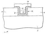
- FIG. 1is an enlarged view of a section of a semiconductor wafer at one processing step in accordance with the invention.
- FIG. 2is an enlarged view of the section of the FIG. 1 wafer at a processing step subsequent to that depicted by FIG. 1 .
- FIG. 3is an enlarged view of the section of the FIG. 1 wafer at a processing step subsequent to that depicted by FIG. 2 .
- FIG. 4is an enlarged view of the section of the FIG. 1 wafer at a processing step subsequent to that depicted by FIG. 3 .
- FIG. 5is an enlarged view of the section of the FIG. 1 wafer at a processing step subsequent to that depicted by FIG. 4 .
- FIG. 6is an enlarged view of the section of the FIG. 1 wafer at a processing step subsequent to that depicted by FIG. 5 .
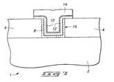
- FIG. 7is an enlarged view of a section of an alternate embodiment semiconductor wafer processed in accordance with alternate aspects of the invention.
- Atomic layer depositioninvolves formation of successive atomic layers on a substrate. Such layers may comprise an epitaxial, polycrystalline, amorphous, etc. material. ALD may also be referred to as atomic layer epitaxy, atomic layer processing, etc. Further, the invention may encompass other deposition methods not traditionally referred to as ALD, for example, chemical vapor deposition (CVD), but nevertheless including the method steps described herein. The deposition methods herein may be described in the context of formation on a semiconductor wafer. However, the invention encompasses deposition on a variety of substrates besides semiconductor substrates.
- semiconductor substrateor “semiconductive substrate” is defined to mean any construction comprising semiconductive material, including, but not limited to, bulk semiconductive materials such as a semiconductive wafer (either alone or in assemblies comprising other materials thereon), and semiconductive material layers (either alone or in assemblies comprising other materials).
- substraterefers to any supporting structure, including, but not limited to, the semiconductive substrates described above.
- ALDincludes exposing an initial substrate to a first chemical species to accomplish chemisorption of the species onto the substrate.
- the chemisorptionforms a monolayer that is uniformly one atom or molecule thick on the entire exposed initial substrate.
- a saturated monolayerPractically, as further described below, chemisorption might not occur on all portions of the substrate. Nevertheless, such an imperfect monolayer is still a monolayer in the context of this document. In many applications, merely a substantially saturated monolayer may be suitable.
- a substantially saturated monolayeris one that will still yield a deposited layer exhibiting the quality and/or properties desired for such layer.
- the first speciesis purged from over the substrate and a second chemical species is provided to chemisorb onto the first monolayer of the first species.
- the second speciesis then purged and the steps are repeated with exposure of the second species monolayer to the first species.
- the two monolayersmay be of the same species.
- a third species or moremay be successively chemisorbed and purged just as described for the first and second species.
- Purgingmay involve a variety of techniques including, but not limited to, contacting the substrate and/or monolayer with a carrier gas and/or lowering pressure to below the deposition pressure to reduce the concentration of a species contacting the substrate and/or chemisorbed species.
- carrier gasesinclude N 2 , Ar, He, Ne, Kr, Xe, etc.
- Purgingmay instead include contacting the substrate and/or monolayer with any substance that allows chemisorption byproducts to desorb and reduces the concentration of a contacting species preparatory to introducing another species.
- a suitable amount of purgingcan be determined experimentally as known to those skilled in the art.
- Purging timemay be successively reduced to a purge time that yields an increase in film growth rate.
- the increase in film growth ratemight be an indication of a change to a non-ALD process regime and may be used to establish a purge time limit.
- ALDis often described as a self-limiting process, in that a finite number of sites exist on a substrate to which the first species may form chemical bonds. The second species might only bond to the first species and thus may also be self-limiting. Once all of the finite number of sites on a substrate are bonded with a first species, the first species will often not bond to other of the first species already bonded with the substrate.
- process conditionscan be varied in ALD to promote such bonding and render ALD not self-limiting. Accordingly, ALD may also encompass a species forming other than one monolayer at a time by stacking of a species, forming a layer more than one atom or molecule thick.
- ALDatomic layer deposition
- CVDchemical vapor deposition
- plasma enhanced CVDplasma enhanced CVD
- CVDis commonly used to form non-selectively a complete, deposited material on a substrate.
- One characteristic of CVDis the simultaneous presence of multiple species in the deposition chamber that react to form the deposited material. Such condition is contrasted with the purging criteria for traditional ALD wherein a substrate is contacted with a single deposition species that chemisorbs to a substrate or previously deposited species.
- An ALD process regimemay provide a simultaneously contacted plurality of species of a type or under conditions such that ALD chemisorption, rather than CVD reaction occurs.
- the speciesmay chemisorb to a substrate or previously deposited species, providing a surface onto which subsequent species may next chemisorb to form a complete layer of desired material.
- depositionoccurs largely independent of the composition or surface properties of an underlying substrate.
- chemisorption rate in ALDmight be influenced by the composition, crystalline structure, and other properties of a substrate or chemisorbed species.
- Other process conditionsfor example, pressure and temperature, may also influence chemisorption rate.
- a capacitor fabrication methodincludes forming a first capacitor electrode over a substrate and atomic layer depositing an insulative barrier layer to oxygen diffusion over the first electrode.
- a capacitor dielectric layermay be formed over the first electrode and a second capacitor electrode may be formed over the dielectric layer.
- At least one of the first or second electrodesmay comprise polysilicon, which may be rugged polysilicon, preferably hemispherical grain (HSG) polysilicon.
- HSGhemispherical grain
- the electrodesmight comprise RuO x .
- the dielectric layermay comprise oxygen.
- Exemplary materials for the dielectric layerinclude, but are not limited to, Ta 2 O 5 , barium strontium titanate, TiO 2 , Y 2 O 3 , HfO 2 , ZrO 2 , HfSiO 2 , ZrSiO 2 , etc.
- the insulative barrier layer to oxygen diffusion formed over the first electrodemay provide the advantage of reducing oxidation of the electrode by oxygen diffusion from an oxygen source, for example, the dielectric layer.
- the dielectricmay be formed over the barrier layer, thus, the barrier layer may reduce oxygen diffusion to the first capacitor electrode.
- such barrier layermay reduce oxygen diffusion from the first capacitor electrode or under the first capacitor electrode to the dielectric layer or second capacitor electrode.
- the barrier layermay also be formed over the capacitor dielectric layer with the second capacitor electrode over the barrier layer such that the barrier layer reduces oxygen diffusion from the dielectric layer to the second electrode.
- Such positioningmay also reduce oxygen diffusion from over the dielectric layer to the first capacitor electrode, for example, oxygen diffusion from the second capacitor electrode.
- Suchmay be a problem when the second capacitor electrode comprises RuO x .
- one aspect of the inventionmay include atomic layer depositing the barrier layer over the first electrode, forming the dielectric layer over the barrier layer, and atomic layer depositing another conductive barrier layer to oxygen diffusion over the dielectric layer.
- Forming the first and second electrodes and dielectric layermay be accomplished by methods known to those skilled in the art and may include atomic layer deposition, but preferably other methods.
- the atomic layer depositing of the barrier layermay occur at a temperature of from about 100 to about 600° C. and at a pressure of from about 100 milliTorr (mT) to about 10 Torr (T).
- the atomic layer deposited barrier layermay exhibit a K factor of greater than about 7 at 20° C.
- the barrier layermay exhibit a K factor of about 10 at 20° C.
- One particularly suitable material for the barrier layerincludes Al 2 O 3 .
- the barrier layermay have a thickness of less than about 30 Angstroms or another thickness depending on the material properties.
- the barrier layermay have a thickness of less than about 12 Angstroms, or more preferably less than about 6 Angstroms.
- a 30 Angstrom film of Al 2 O 3protected a WN film from oxidation during annealing at 700° C. for 60 seconds in an O 2 ambient. Thinner Al 2 O 3 films may also be suitable.
- an “insulative” material as the term is used hereindesignates a material exhibiting a conductivity at 20° C. of less than 10 4 microOhm ⁇ 1 centimeter ⁇ 1 .
- an “insulative” material in the present contextmight be viewed as a material that impacts the capacitance otherwise achieved without the material.
- a “conductive” or “semiconductive” materialmight not produce a change in capacitance as such a barrier layer.
- a combined capacitor dielectric and insulative barrier layer according to the aspects of the inventioncan exhibit a leakage current of less than about 10 ⁇ 15 amps per cell and yield a capacitance of greater than about 20 femtoFarads per cell.
- One example of a precursor pair for forming Al 2 O 3includes H 2 O and trimethyl aluminum (TMA). It is conceivable that more than one pair of precursors may comprise the first and second precursors, but preferably only one pair. Additional alternating first and second precursor layers may be chemisorbed in keeping with the above aspect of the invention to achieve a desired thickness for the barrier layer.
- TMAtrimethyl aluminum
- FIGS. 1-6exemplify the features of the various aspects of the invention described above, as well as other aspects of the invention. For example, enhancing capacitance per unit area.
- wafer portion 1is shown including a substrate 2 with an insulative layer 4 formed thereon.
- a capacitor fabrication methodmay include forming an opening 16 in insulative layer 4 , the opening 16 having sides and a bottom.
- a layer of polysilicon 6may be formed over the sides and bottom of the opening.
- Polysilicon layer 6may then be converted to a first capacitor electrode 8 comprising hemispherical grain polysilicon, as shown in FIG. 3 .
- an insulative barrier layer 10may be conformally formed on first electrode 8 .
- Barrier layer 10may comprise Al 2 O 3 and be sufficiently thick and dense to reduce oxidation of the first electrode by oxygen diffusion from over barrier layer 10 .
- a capacitor dielectric layer 12may be formed on barrier layer 10 .
- One source of oxygen diffusionmay be dielectric layer 12 .
- a second capacitor electrode layer 14is shown formed on dielectric layer 12 .
- FIG. 6shows excess portions of barrier layer 10 , dielectric layer 12 , and second capacitor electrode layer 14 removed from over insulative layer 4 to form a capacitor structure.
- a barrier layermay also be formed over a dielectric layer, thus FIG. 7 alternatively shows barrier layer 10 over dielectric layer 12 .
Landscapes
- Semiconductor Memories (AREA)
- Semiconductor Integrated Circuits (AREA)
Abstract
Description
Claims (31)
Priority Applications (2)
| Application Number | Priority Date | Filing Date | Title |
|---|---|---|---|
| US09/652,532US6420230B1 (en) | 2000-08-31 | 2000-08-31 | Capacitor fabrication methods and capacitor constructions |
| US09/882,534US7053432B2 (en) | 2000-08-31 | 2001-06-14 | Enhanced surface area capacitor fabrication methods |
Applications Claiming Priority (1)
| Application Number | Priority Date | Filing Date | Title |
|---|---|---|---|
| US09/652,532US6420230B1 (en) | 2000-08-31 | 2000-08-31 | Capacitor fabrication methods and capacitor constructions |
Related Child Applications (1)
| Application Number | Title | Priority Date | Filing Date |
|---|---|---|---|
| US09/882,534DivisionUS7053432B2 (en) | 2000-08-31 | 2001-06-14 | Enhanced surface area capacitor fabrication methods |
Publications (1)
| Publication Number | Publication Date |
|---|---|
| US6420230B1true US6420230B1 (en) | 2002-07-16 |
Family
ID=24617172
Family Applications (2)
| Application Number | Title | Priority Date | Filing Date |
|---|---|---|---|
| US09/652,532Expired - LifetimeUS6420230B1 (en) | 2000-08-31 | 2000-08-31 | Capacitor fabrication methods and capacitor constructions |
| US09/882,534Expired - Fee RelatedUS7053432B2 (en) | 2000-08-31 | 2001-06-14 | Enhanced surface area capacitor fabrication methods |
Family Applications After (1)
| Application Number | Title | Priority Date | Filing Date |
|---|---|---|---|
| US09/882,534Expired - Fee RelatedUS7053432B2 (en) | 2000-08-31 | 2001-06-14 | Enhanced surface area capacitor fabrication methods |
Country Status (1)
| Country | Link |
|---|---|
| US (2) | US6420230B1 (en) |
Cited By (63)
| Publication number | Priority date | Publication date | Assignee | Title |
|---|---|---|---|---|
| US20020024080A1 (en)* | 2000-08-31 | 2002-02-28 | Derderian Garo J. | Capacitor fabrication methods and capacitor constructions |
| US20020094632A1 (en)* | 2000-08-31 | 2002-07-18 | Agarwal Vishnu K. | Capacitor fabrication methods and capacitor constructions |
| US20020102818A1 (en)* | 2000-08-31 | 2002-08-01 | Sandhu Gurtej S. | Deposition methods and apparatuses providing surface activation |
| US20030031787A1 (en)* | 2001-08-09 | 2003-02-13 | Doan Trung Tri | Variable temperature deposition methods |
| US6596602B2 (en)* | 2001-01-29 | 2003-07-22 | Nec Corporation | Method of fabricating a high dielectric constant metal oxide capacity insulator film using atomic layer CVD |
| US20030201034A1 (en)* | 2002-04-25 | 2003-10-30 | Marsh Eugene P. | Metal layer forming methods and capacitor electrode forming methods |
| US20030226500A1 (en)* | 2002-06-05 | 2003-12-11 | Derderian Garo J. | Atomic layer deposition apparatus and methods |
| US20040018307A1 (en)* | 2002-07-26 | 2004-01-29 | Park In-Sung | Methods of forming atomic layers of a material on a substrate by sequentially introducing precursors of the material |
| US20040041194A1 (en)* | 2002-08-29 | 2004-03-04 | Micron Technology, Inc. | Metal plating using seed film |
| US20040062863A1 (en)* | 2000-07-19 | 2004-04-01 | Derderian Garo J. | Deposition methods |
| US20040065258A1 (en)* | 2002-10-08 | 2004-04-08 | Sandhu Gurtej S. | Atomic layer deposition methods and atomic layer deposition tools |
| US20040087081A1 (en)* | 2002-11-01 | 2004-05-06 | Aitchison Bradley J. | Capacitor fabrication methods and capacitor structures including niobium oxide |
| US20050020017A1 (en)* | 2003-06-24 | 2005-01-27 | Micron Technology, Inc. | Lanthanide oxide / hafnium oxide dielectric layers |
| US20050018381A1 (en)* | 2003-07-21 | 2005-01-27 | Mcclure Brent A. | Capacitor constructions and methods of forming |
| US6852167B2 (en) | 2001-03-01 | 2005-02-08 | Micron Technology, Inc. | Methods, systems, and apparatus for uniform chemical-vapor depositions |
| US20050054165A1 (en)* | 2003-03-31 | 2005-03-10 | Micron Technology, Inc. | Atomic layer deposited ZrAlxOy dielectric layers |
| US20050051824A1 (en)* | 2001-06-13 | 2005-03-10 | Toshihiro Iizuka | Semiconductor device having a thin film capacitor and method for fabricating the same |
| US20050064212A1 (en)* | 2001-02-23 | 2005-03-24 | Dunlap Paul N. | Bonded part and method for producing same |
| US20050100669A1 (en)* | 2003-11-12 | 2005-05-12 | Veeco Instruments, Inc. | Method and apparatus for fabricating a conformal thin film on a substrate |
| US20050170532A1 (en)* | 2004-01-30 | 2005-08-04 | Headway Technologies, Inc. | Novel oxidation method to fabricate low resistance TMR read head |
| US7037574B2 (en)* | 2001-05-23 | 2006-05-02 | Veeco Instruments, Inc. | Atomic layer deposition for fabricating thin films |
| US7045430B2 (en) | 2002-05-02 | 2006-05-16 | Micron Technology Inc. | Atomic layer-deposited LaAlO3 films for gate dielectrics |
| US7056806B2 (en) | 2003-09-17 | 2006-06-06 | Micron Technology, Inc. | Microfeature workpiece processing apparatus and methods for controlling deposition of materials on microfeature workpieces |
| US7084078B2 (en) | 2002-08-29 | 2006-08-01 | Micron Technology, Inc. | Atomic layer deposited lanthanide doped TiOx dielectric films |
| US20060177975A1 (en)* | 2005-02-10 | 2006-08-10 | Micron Technology, Inc. | Atomic layer deposition of CeO2/Al2O3 films as gate dielectrics |
| US7094704B2 (en)* | 2002-05-09 | 2006-08-22 | Applied Materials, Inc. | Method of plasma etching of high-K dielectric materials |
| US7108747B1 (en)* | 1998-09-11 | 2006-09-19 | Asm International N.V. | Method for growing oxide thin films containing barium and strontium |
| US20060251813A1 (en)* | 2004-04-08 | 2006-11-09 | Carlson Chris M | Methods of forming material over substrates |
| US20060272577A1 (en)* | 2005-06-03 | 2006-12-07 | Ming Mao | Method and apparatus for decreasing deposition time of a thin film |
| US7160577B2 (en) | 2002-05-02 | 2007-01-09 | Micron Technology, Inc. | Methods for atomic-layer deposition of aluminum oxides in integrated circuits |
| US7192892B2 (en) | 2003-03-04 | 2007-03-20 | Micron Technology, Inc. | Atomic layer deposited dielectric layers |
| CN1319128C (en)* | 2003-01-02 | 2007-05-30 | 上海华虹(集团)有限公司 | High dielectric grid laminating structure |
| US7235138B2 (en) | 2003-08-21 | 2007-06-26 | Micron Technology, Inc. | Microfeature workpiece processing apparatus and methods for batch deposition of materials on microfeature workpieces |
| US20070190775A1 (en)* | 2000-08-21 | 2007-08-16 | Mercaldi Garry A | Low selectivity deposition methods |
| US7258892B2 (en) | 2003-12-10 | 2007-08-21 | Micron Technology, Inc. | Methods and systems for controlling temperature during microfeature workpiece processing, e.g., CVD deposition |
| US7282239B2 (en) | 2003-09-18 | 2007-10-16 | Micron Technology, Inc. | Systems and methods for depositing material onto microfeature workpieces in reaction chambers |
| US7323231B2 (en) | 2003-10-09 | 2008-01-29 | Micron Technology, Inc. | Apparatus and methods for plasma vapor deposition processes |
| US7335396B2 (en) | 2003-04-24 | 2008-02-26 | Micron Technology, Inc. | Methods for controlling mass flow rates and pressures in passageways coupled to reaction chambers and systems for depositing material onto microfeature workpieces in reaction chambers |
| US7344755B2 (en) | 2003-08-21 | 2008-03-18 | Micron Technology, Inc. | Methods and apparatus for processing microfeature workpieces; methods for conditioning ALD reaction chambers |
| US7387685B2 (en) | 2002-07-08 | 2008-06-17 | Micron Technology, Inc. | Apparatus and method for depositing materials onto microelectronic workpieces |
| US7422635B2 (en) | 2003-08-28 | 2008-09-09 | Micron Technology, Inc. | Methods and apparatus for processing microfeature workpieces, e.g., for depositing materials on microfeature workpieces |
| US7429515B2 (en) | 2001-12-20 | 2008-09-30 | Micron Technology, Inc. | Low-temperature grown high quality ultra-thin CoTiO3 gate dielectrics |
| US7481887B2 (en) | 2002-05-24 | 2009-01-27 | Micron Technology, Inc. | Apparatus for controlling gas pulsing in processes for depositing materials onto micro-device workpieces |
| US7554161B2 (en) | 2002-06-05 | 2009-06-30 | Micron Technology, Inc. | HfAlO3 films for gate dielectrics |
| US7560793B2 (en) | 2002-05-02 | 2009-07-14 | Micron Technology, Inc. | Atomic layer deposition and conversion |
| US7582549B2 (en) | 2006-08-25 | 2009-09-01 | Micron Technology, Inc. | Atomic layer deposited barium strontium titanium oxide films |
| US7581511B2 (en) | 2003-10-10 | 2009-09-01 | Micron Technology, Inc. | Apparatus and methods for manufacturing microfeatures on workpieces using plasma vapor processes |
| US7584942B2 (en) | 2004-03-31 | 2009-09-08 | Micron Technology, Inc. | Ampoules for producing a reaction gas and systems for depositing materials onto microfeature workpieces in reaction chambers |
| US7588988B2 (en) | 2004-08-31 | 2009-09-15 | Micron Technology, Inc. | Method of forming apparatus having oxide films formed using atomic layer deposition |
| US7588804B2 (en) | 2002-08-15 | 2009-09-15 | Micron Technology, Inc. | Reactors with isolated gas connectors and methods for depositing materials onto micro-device workpieces |
| US7647886B2 (en) | 2003-10-15 | 2010-01-19 | Micron Technology, Inc. | Systems for depositing material onto workpieces in reaction chambers and methods for removing byproducts from reaction chambers |
| US7662729B2 (en) | 2005-04-28 | 2010-02-16 | Micron Technology, Inc. | Atomic layer deposition of a ruthenium layer to a lanthanide oxide dielectric layer |
| US7687409B2 (en) | 2005-03-29 | 2010-03-30 | Micron Technology, Inc. | Atomic layer deposited titanium silicon oxide films |
| US7699932B2 (en) | 2004-06-02 | 2010-04-20 | Micron Technology, Inc. | Reactors, systems and methods for depositing thin films onto microfeature workpieces |
| US7728626B2 (en) | 2002-07-08 | 2010-06-01 | Micron Technology, Inc. | Memory utilizing oxide nanolaminates |
| US7869242B2 (en) | 1999-07-30 | 2011-01-11 | Micron Technology, Inc. | Transmission lines for CMOS integrated circuits |
| US7906393B2 (en) | 2004-01-28 | 2011-03-15 | Micron Technology, Inc. | Methods for forming small-scale capacitor structures |
| US20110223320A1 (en)* | 2010-03-09 | 2011-09-15 | Zhe Song | Methods Of Forming Material Over A Substrate And Methods Of Forming Capacitors |
| US8133554B2 (en) | 2004-05-06 | 2012-03-13 | Micron Technology, Inc. | Methods for depositing material onto microfeature workpieces in reaction chambers and systems for depositing materials onto microfeature workpieces |
| US20120178256A1 (en)* | 2001-02-02 | 2012-07-12 | Seutter Sean M | Formation of a tantalum-nitride layer |
| US8501563B2 (en) | 2005-07-20 | 2013-08-06 | Micron Technology, Inc. | Devices with nanocrystals and methods of formation |
| US9062390B2 (en) | 2011-09-12 | 2015-06-23 | Asm International N.V. | Crystalline strontium titanate and methods of forming the same |
| US9365926B2 (en) | 2010-02-25 | 2016-06-14 | Asm International N.V. | Precursors and methods for atomic layer deposition of transition metal oxides |
Families Citing this family (23)
| Publication number | Priority date | Publication date | Assignee | Title |
|---|---|---|---|---|
| US7192827B2 (en)* | 2001-01-05 | 2007-03-20 | Micron Technology, Inc. | Methods of forming capacitor structures |
| KR100393209B1 (en)* | 2001-01-18 | 2003-07-31 | 삼성전자주식회사 | A method for formation of semiconductor capacitor having Ta2O5 film as dielectric layer |
| US6893984B2 (en)* | 2002-02-20 | 2005-05-17 | Micron Technology Inc. | Evaporated LaA1O3 films for gate dielectrics |
| JP2004039821A (en)* | 2002-07-02 | 2004-02-05 | Elpida Memory Inc | Method for manufacturing semiconductor device |
| US6921702B2 (en)* | 2002-07-30 | 2005-07-26 | Micron Technology Inc. | Atomic layer deposited nanolaminates of HfO2/ZrO2 films as gate dielectrics |
| US6884739B2 (en)* | 2002-08-15 | 2005-04-26 | Micron Technology Inc. | Lanthanide doped TiOx dielectric films by plasma oxidation |
| US6790791B2 (en)* | 2002-08-15 | 2004-09-14 | Micron Technology, Inc. | Lanthanide doped TiOx dielectric films |
| US7199023B2 (en)* | 2002-08-28 | 2007-04-03 | Micron Technology, Inc. | Atomic layer deposited HfSiON dielectric films wherein each precursor is independendently pulsed |
| US6958302B2 (en)* | 2002-12-04 | 2005-10-25 | Micron Technology, Inc. | Atomic layer deposited Zr-Sn-Ti-O films using TiI4 |
| US7101813B2 (en)* | 2002-12-04 | 2006-09-05 | Micron Technology Inc. | Atomic layer deposited Zr-Sn-Ti-O films |
| US7220665B2 (en)* | 2003-08-05 | 2007-05-22 | Micron Technology, Inc. | H2 plasma treatment |
| US7601649B2 (en)* | 2004-08-02 | 2009-10-13 | Micron Technology, Inc. | Zirconium-doped tantalum oxide films |
| US7081421B2 (en) | 2004-08-26 | 2006-07-25 | Micron Technology, Inc. | Lanthanide oxide dielectric layer |
| US7494939B2 (en)* | 2004-08-31 | 2009-02-24 | Micron Technology, Inc. | Methods for forming a lanthanum-metal oxide dielectric layer |
| US20060125030A1 (en)* | 2004-12-13 | 2006-06-15 | Micron Technology, Inc. | Hybrid ALD-CVD of PrxOy/ZrO2 films as gate dielectrics |
| US7235501B2 (en) | 2004-12-13 | 2007-06-26 | Micron Technology, Inc. | Lanthanum hafnium oxide dielectrics |
| US7560395B2 (en)* | 2005-01-05 | 2009-07-14 | Micron Technology, Inc. | Atomic layer deposited hafnium tantalum oxide dielectrics |
| US7508648B2 (en)* | 2005-02-08 | 2009-03-24 | Micron Technology, Inc. | Atomic layer deposition of Dy doped HfO2 films as gate dielectrics |
| US7393736B2 (en)* | 2005-08-29 | 2008-07-01 | Micron Technology, Inc. | Atomic layer deposition of Zrx Hfy Sn1-x-y O2 films as high k gate dielectrics |
| US7410910B2 (en) | 2005-08-31 | 2008-08-12 | Micron Technology, Inc. | Lanthanum aluminum oxynitride dielectric films |
| US7709402B2 (en)* | 2006-02-16 | 2010-05-04 | Micron Technology, Inc. | Conductive layers for hafnium silicon oxynitride films |
| US7605030B2 (en)* | 2006-08-31 | 2009-10-20 | Micron Technology, Inc. | Hafnium tantalum oxynitride high-k dielectric and metal gates |
| US7759237B2 (en) | 2007-06-28 | 2010-07-20 | Micron Technology, Inc. | Method of forming lutetium and lanthanum dielectric structures |
Citations (19)
| Publication number | Priority date | Publication date | Assignee | Title |
|---|---|---|---|---|
| US5316982A (en)* | 1991-10-18 | 1994-05-31 | Sharp Kabushiki Kaisha | Semiconductor device and method for preparing the same |
| US5432732A (en)* | 1991-01-01 | 1995-07-11 | Ohmi; Tadahiro | Dynamic semiconductor memory |
| US5641984A (en)* | 1994-08-19 | 1997-06-24 | General Electric Company | Hermetically sealed radiation imager |
| US6104049A (en) | 1997-03-03 | 2000-08-15 | Symetrix Corporation | Ferroelectric memory with ferroelectric thin film having thickness of 90 nanometers or less, and method of making same |
| US6124158A (en)* | 1999-06-08 | 2000-09-26 | Lucent Technologies Inc. | Method of reducing carbon contamination of a thin dielectric film by using gaseous organic precursors, inert gas, and ozone to react with carbon contaminants |
| US6144060A (en)* | 1997-07-31 | 2000-11-07 | Samsung Electronics Co., Ltd. | Integrated circuit devices having buffer layers therein which contain metal oxide stabilized by heat treatment under low temperature |
| US6156606A (en)* | 1998-11-17 | 2000-12-05 | Siemens Aktiengesellschaft | Method of forming a trench capacitor using a rutile dielectric material |
| US6174770B1 (en) | 1999-10-14 | 2001-01-16 | Taiwan Semiconductor Manufacturing Co., Ltd. | Method for forming a crown capacitor having HSG for DRAM memory |
| US6180481B1 (en) | 1998-01-09 | 2001-01-30 | Micron Technology, Inc. | Barrier layer fabrication methods |
| US6180447B1 (en) | 1997-02-27 | 2001-01-30 | Samsung Electronics Co., Ltd. | Methods for fabricating integrated circuit capacitors including barrier layers having grain boundary filling material |
| US6204172B1 (en) | 1998-09-03 | 2001-03-20 | Micron Technology, Inc. | Low temperature deposition of barrier layers |
| US6218260B1 (en)* | 1997-04-22 | 2001-04-17 | Samsung Electronics Co., Ltd. | Methods of forming integrated circuit capacitors having improved electrode and dielectric layer characteristics and capacitors formed thereby |
| US6218256B1 (en) | 1999-04-13 | 2001-04-17 | Micron Technology, Inc. | Electrode and capacitor structure for a semiconductor device and associated methods of manufacture |
| US6242299B1 (en)* | 1999-04-01 | 2001-06-05 | Ramtron International Corporation | Barrier layer to protect a ferroelectric capacitor after contact has been made to the capacitor electrode |
| US6249056B1 (en)* | 1997-08-16 | 2001-06-19 | Samsung Electronics Co., Ltd. | Low resistance interconnect for a semiconductor device and method of fabricating the same |
| US6274428B1 (en)* | 1999-04-22 | 2001-08-14 | Acer Semiconductor Manufacturing Inc. | Method for forming a ragged polysilicon crown-shaped capacitor for a memory cell |
| US6281142B1 (en) | 1999-06-04 | 2001-08-28 | Micron Technology, Inc. | Dielectric cure for reducing oxygen vacancies |
| US6291289B2 (en) | 1999-06-25 | 2001-09-18 | Micron Technology, Inc. | Method of forming DRAM trench capacitor with metal layer over hemispherical grain polysilicon |
| US6335240B1 (en)* | 1998-01-06 | 2002-01-01 | Samsung Electronics Co., Ltd. | Capacitor for a semiconductor device and method for forming the same |
Family Cites Families (43)
| Publication number | Priority date | Publication date | Assignee | Title |
|---|---|---|---|---|
| US5126283A (en)* | 1990-05-21 | 1992-06-30 | Motorola, Inc. | Process for the selective encapsulation of an electrically conductive structure in a semiconductor device |
| US5330931A (en)* | 1993-09-22 | 1994-07-19 | Northern Telecom Limited | Method of making a capacitor for an integrated circuit |
| US5625233A (en)* | 1995-01-13 | 1997-04-29 | Ibm Corporation | Thin film multi-layer oxygen diffusion barrier consisting of refractory metal, refractory metal aluminide, and aluminum oxide |
| US5885882A (en) | 1995-07-18 | 1999-03-23 | Micron Technology, Inc. | Method for making polysilicon electrode with increased surface area making same |
| US5811344A (en) | 1997-01-27 | 1998-09-22 | Mosel Vitelic Incorporated | Method of forming a capacitor of a dram cell |
| US6069053A (en) | 1997-02-28 | 2000-05-30 | Micron Technology, Inc. | Formation of conductive rugged silicon |
| KR100269309B1 (en)* | 1997-09-29 | 2000-10-16 | 윤종용 | Ferroelectric memory devices and fabrication methods therefor |
| KR100436058B1 (en)* | 1997-12-27 | 2004-12-17 | 주식회사 하이닉스반도체 | How to Form Ferroelectric Capacitors |
| JP3630551B2 (en) | 1998-04-02 | 2005-03-16 | 株式会社東芝 | Semiconductor memory device and manufacturing method thereof |
| KR100275738B1 (en)* | 1998-08-07 | 2000-12-15 | 윤종용 | Method for producing thin film using atomatic layer deposition |
| KR100327328B1 (en)* | 1998-10-13 | 2002-05-09 | 윤종용 | Method for forming dielectric layer of capacitor having partially different thickness in the layer |
| JP2000183311A (en) | 1998-12-17 | 2000-06-30 | Nec Corp | Semiconductor device and manufacturing method thereof |
| KR100371142B1 (en)* | 1998-12-30 | 2003-03-31 | 주식회사 하이닉스반도체 | Capacitor Formation Method of Semiconductor Device |
| US6033987A (en) | 1999-01-15 | 2000-03-07 | Winbond Electronics Corp. | Method for mapping and adjusting pressure distribution of CMP processes |
| JP2000216356A (en) | 1999-01-21 | 2000-08-04 | Nec Corp | Semiconductor device and manufacturing method thereof |
| KR100329781B1 (en)* | 1999-06-28 | 2002-03-25 | 박종섭 | Method for forming feram capable of preventing hydrogen diffusion |
| US6281543B1 (en)* | 1999-08-31 | 2001-08-28 | Micron Technology, Inc. | Double layer electrode and barrier system on hemispherical grain silicon for use with high dielectric constant materials and methods for fabricating the same |
| US6780704B1 (en) | 1999-12-03 | 2004-08-24 | Asm International Nv | Conformal thin films over textured capacitor electrodes |
| US6551399B1 (en) | 2000-01-10 | 2003-04-22 | Genus Inc. | Fully integrated process for MIM capacitors using atomic layer deposition |
| US6417537B1 (en)* | 2000-01-18 | 2002-07-09 | Micron Technology, Inc. | Metal oxynitride capacitor barrier layer |
| US7253076B1 (en) | 2000-06-08 | 2007-08-07 | Micron Technologies, Inc. | Methods for forming and integrated circuit structures containing ruthenium and tungsten containing layers |
| KR20020001376A (en)* | 2000-06-28 | 2002-01-09 | 박종섭 | Method of forming a Al2O3 layer in a semiconductor device |
| KR100342873B1 (en)* | 2000-06-29 | 2002-07-02 | 박종섭 | Method for forming capacitor of semiconductor device |
| US6458416B1 (en)* | 2000-07-19 | 2002-10-01 | Micron Technology, Inc. | Deposition methods |
| US6309923B1 (en)* | 2000-07-20 | 2001-10-30 | Vanguard International Semiconductor Corporation | Method of forming the capacitor in DRAM |
| US6664186B1 (en)* | 2000-09-29 | 2003-12-16 | International Business Machines Corporation | Method of film deposition, and fabrication of structures |
| KR100384851B1 (en)* | 2000-12-14 | 2003-05-22 | 주식회사 하이닉스반도체 | Method for fabricating capacitor by Atomic Layer Deposition |
| JP2002222934A (en)* | 2001-01-29 | 2002-08-09 | Nec Corp | Semiconductor device and method of manufacturing the same |
| KR100406536B1 (en)* | 2001-03-28 | 2003-11-20 | 주식회사 하이닉스반도체 | FeRAM having aluminum oxide layer as oxygen diffusion barrier and method for forming the same |
| JP2002314072A (en)* | 2001-04-19 | 2002-10-25 | Nec Corp | Semiconductor device provided with high dielectric thin film, method for manufacturing the same, and apparatus for forming dielectric film |
| KR100414156B1 (en)* | 2001-05-29 | 2004-01-07 | 삼성전자주식회사 | Method for manufacturing capacitor in integrated circuits device |
| US6391803B1 (en)* | 2001-06-20 | 2002-05-21 | Samsung Electronics Co., Ltd. | Method of forming silicon containing thin films by atomic layer deposition utilizing trisdimethylaminosilane |
| KR100420121B1 (en)* | 2001-06-21 | 2004-03-02 | 삼성전자주식회사 | Ferroelectric device using ferroelectric layer as planarization layer and method of forming the same |
| US6746930B2 (en)* | 2001-07-11 | 2004-06-08 | Micron Technology, Inc. | Oxygen barrier for cell container process |
| KR100415538B1 (en)* | 2001-09-14 | 2004-01-24 | 주식회사 하이닉스반도체 | Capacitor with double dielectric layer and method for fabricating the same |
| US6824816B2 (en) | 2002-01-29 | 2004-11-30 | Asm International N.V. | Process for producing metal thin films by ALD |
| JP2003338608A (en) | 2002-05-20 | 2003-11-28 | Oki Electric Ind Co Ltd | Ferroelectric capacitor and method of manufacturing the same |
| KR100468852B1 (en)* | 2002-07-20 | 2005-01-29 | 삼성전자주식회사 | Manufacturing method of Capacitor Structure |
| KR100450681B1 (en)* | 2002-08-16 | 2004-10-02 | 삼성전자주식회사 | Capacitor of semiconductor memory device and manufacturing method thereof |
| KR100540474B1 (en)* | 2002-12-30 | 2006-01-11 | 주식회사 하이닉스반도체 | Capacitor with Oxygen Diffusion Prevention Film and Manufacturing Method Thereof |
| US6800892B2 (en) | 2003-02-10 | 2004-10-05 | Micron Technology, Inc. | Memory devices, and electronic systems comprising memory devices |
| US7440255B2 (en) | 2003-07-21 | 2008-10-21 | Micron Technology, Inc. | Capacitor constructions and methods of forming |
| KR101001741B1 (en)* | 2003-08-18 | 2010-12-15 | 삼성전자주식회사 | A capacitor of a semiconductor device, a method of manufacturing the same, and a memory device having a capacitor |
- 2000
- 2000-08-31USUS09/652,532patent/US6420230B1/ennot_activeExpired - Lifetime
- 2001
- 2001-06-14USUS09/882,534patent/US7053432B2/ennot_activeExpired - Fee Related
Patent Citations (19)
| Publication number | Priority date | Publication date | Assignee | Title |
|---|---|---|---|---|
| US5432732A (en)* | 1991-01-01 | 1995-07-11 | Ohmi; Tadahiro | Dynamic semiconductor memory |
| US5316982A (en)* | 1991-10-18 | 1994-05-31 | Sharp Kabushiki Kaisha | Semiconductor device and method for preparing the same |
| US5641984A (en)* | 1994-08-19 | 1997-06-24 | General Electric Company | Hermetically sealed radiation imager |
| US6180447B1 (en) | 1997-02-27 | 2001-01-30 | Samsung Electronics Co., Ltd. | Methods for fabricating integrated circuit capacitors including barrier layers having grain boundary filling material |
| US6104049A (en) | 1997-03-03 | 2000-08-15 | Symetrix Corporation | Ferroelectric memory with ferroelectric thin film having thickness of 90 nanometers or less, and method of making same |
| US6218260B1 (en)* | 1997-04-22 | 2001-04-17 | Samsung Electronics Co., Ltd. | Methods of forming integrated circuit capacitors having improved electrode and dielectric layer characteristics and capacitors formed thereby |
| US6144060A (en)* | 1997-07-31 | 2000-11-07 | Samsung Electronics Co., Ltd. | Integrated circuit devices having buffer layers therein which contain metal oxide stabilized by heat treatment under low temperature |
| US6249056B1 (en)* | 1997-08-16 | 2001-06-19 | Samsung Electronics Co., Ltd. | Low resistance interconnect for a semiconductor device and method of fabricating the same |
| US6335240B1 (en)* | 1998-01-06 | 2002-01-01 | Samsung Electronics Co., Ltd. | Capacitor for a semiconductor device and method for forming the same |
| US6180481B1 (en) | 1998-01-09 | 2001-01-30 | Micron Technology, Inc. | Barrier layer fabrication methods |
| US6204172B1 (en) | 1998-09-03 | 2001-03-20 | Micron Technology, Inc. | Low temperature deposition of barrier layers |
| US6156606A (en)* | 1998-11-17 | 2000-12-05 | Siemens Aktiengesellschaft | Method of forming a trench capacitor using a rutile dielectric material |
| US6242299B1 (en)* | 1999-04-01 | 2001-06-05 | Ramtron International Corporation | Barrier layer to protect a ferroelectric capacitor after contact has been made to the capacitor electrode |
| US6218256B1 (en) | 1999-04-13 | 2001-04-17 | Micron Technology, Inc. | Electrode and capacitor structure for a semiconductor device and associated methods of manufacture |
| US6274428B1 (en)* | 1999-04-22 | 2001-08-14 | Acer Semiconductor Manufacturing Inc. | Method for forming a ragged polysilicon crown-shaped capacitor for a memory cell |
| US6281142B1 (en) | 1999-06-04 | 2001-08-28 | Micron Technology, Inc. | Dielectric cure for reducing oxygen vacancies |
| US6124158A (en)* | 1999-06-08 | 2000-09-26 | Lucent Technologies Inc. | Method of reducing carbon contamination of a thin dielectric film by using gaseous organic precursors, inert gas, and ozone to react with carbon contaminants |
| US6291289B2 (en) | 1999-06-25 | 2001-09-18 | Micron Technology, Inc. | Method of forming DRAM trench capacitor with metal layer over hemispherical grain polysilicon |
| US6174770B1 (en) | 1999-10-14 | 2001-01-16 | Taiwan Semiconductor Manufacturing Co., Ltd. | Method for forming a crown capacitor having HSG for DRAM memory |
Non-Patent Citations (3)
| Title |
|---|
| A. W. Ott, et al., "Atomic layer controlled deposition of Al2O3 films using binary reaction sequence chemistry" Applied Surface Science (107) 1996, pp. 128-136. |
| U.S. application No. 09/653,149, Derderian, filed Aug. 31, 2000. |
| U.S. application No. 09/653,156, Agarwal, filed Aug. 31, 2000. |
Cited By (138)
| Publication number | Priority date | Publication date | Assignee | Title |
|---|---|---|---|---|
| US7108747B1 (en)* | 1998-09-11 | 2006-09-19 | Asm International N.V. | Method for growing oxide thin films containing barium and strontium |
| US7869242B2 (en) | 1999-07-30 | 2011-01-11 | Micron Technology, Inc. | Transmission lines for CMOS integrated circuits |
| US20060257570A1 (en)* | 2000-07-19 | 2006-11-16 | Derderian Garo J | Deposition methods |
| US7087535B2 (en) | 2000-07-19 | 2006-08-08 | Micron Technology, Inc. | Deposition methods |
| US20040062863A1 (en)* | 2000-07-19 | 2004-04-01 | Derderian Garo J. | Deposition methods |
| US20070190775A1 (en)* | 2000-08-21 | 2007-08-16 | Mercaldi Garry A | Low selectivity deposition methods |
| US20070178640A1 (en)* | 2000-08-31 | 2007-08-02 | Derderian Garo J | Capacitor fabrication methods and capacitor constructions |
| US20060183322A1 (en)* | 2000-08-31 | 2006-08-17 | Sandhu Gurtej S | Deposition methods and apparatuses providing surface activation |
| US7094690B1 (en)* | 2000-08-31 | 2006-08-22 | Micron Technology, Inc. | Deposition methods and apparatuses providing surface activation |
| US7288808B2 (en) | 2000-08-31 | 2007-10-30 | Micron Technology, Inc. | Capacitor constructions with enhanced surface area |
| US20020094632A1 (en)* | 2000-08-31 | 2002-07-18 | Agarwal Vishnu K. | Capacitor fabrication methods and capacitor constructions |
| US7112503B1 (en)* | 2000-08-31 | 2006-09-26 | Micron Technology, Inc. | Enhanced surface area capacitor fabrication methods |
| US20020102818A1 (en)* | 2000-08-31 | 2002-08-01 | Sandhu Gurtej S. | Deposition methods and apparatuses providing surface activation |
| US20070007572A1 (en)* | 2000-08-31 | 2007-01-11 | Agarwal Vishnu K | Capacitor fabrication methods and capacitor constructions |
| US20020024080A1 (en)* | 2000-08-31 | 2002-02-28 | Derderian Garo J. | Capacitor fabrication methods and capacitor constructions |
| US6596602B2 (en)* | 2001-01-29 | 2003-07-22 | Nec Corporation | Method of fabricating a high dielectric constant metal oxide capacity insulator film using atomic layer CVD |
| US9012334B2 (en)* | 2001-02-02 | 2015-04-21 | Applied Materials, Inc. | Formation of a tantalum-nitride layer |
| US20120178256A1 (en)* | 2001-02-02 | 2012-07-12 | Seutter Sean M | Formation of a tantalum-nitride layer |
| US20050064212A1 (en)* | 2001-02-23 | 2005-03-24 | Dunlap Paul N. | Bonded part and method for producing same |
| US7410668B2 (en) | 2001-03-01 | 2008-08-12 | Micron Technology, Inc. | Methods, systems, and apparatus for uniform chemical-vapor depositions |
| US6852167B2 (en) | 2001-03-01 | 2005-02-08 | Micron Technology, Inc. | Methods, systems, and apparatus for uniform chemical-vapor depositions |
| US7037574B2 (en)* | 2001-05-23 | 2006-05-02 | Veeco Instruments, Inc. | Atomic layer deposition for fabricating thin films |
| US20050051824A1 (en)* | 2001-06-13 | 2005-03-10 | Toshihiro Iizuka | Semiconductor device having a thin film capacitor and method for fabricating the same |
| US8169013B2 (en) | 2001-06-13 | 2012-05-01 | Renesas Electronics Corporation | Metal-insulator-metal (MIM) capacitor having capacitor dielectric material selected from a group consisting of ZRO2, HFO2, (ZRX, HF1-X)O2 (0<x<1), (ZRy, Ti (O<y<1), (Hfz, Ti-z)O2 (O<z<1) and (Zrk, Ti1, Hfm)O2 (O<K, 1, m<1, K+1+m=1) |
| US8815678B2 (en) | 2001-06-13 | 2014-08-26 | Renesas Electronics Corporation | Method for fabricating a metal-insulator-metal (MIM) capacitor having capacitor dielectric layer formed by atomic layer deposition (ALD) |
| US20070152256A1 (en)* | 2001-06-13 | 2007-07-05 | Toshihiro Iizuka | Method for fabricating a metal insulator-metal (MIM) capacitor having capacitor dielectric layer formed by atomic layer deposition (ALD) |
| US20060266282A1 (en)* | 2001-08-09 | 2006-11-30 | Doan Trung T | Variable temperature deposition methods |
| US7368014B2 (en)* | 2001-08-09 | 2008-05-06 | Micron Technology, Inc. | Variable temperature deposition methods |
| US20030031787A1 (en)* | 2001-08-09 | 2003-02-13 | Doan Trung Tri | Variable temperature deposition methods |
| US7804144B2 (en) | 2001-12-20 | 2010-09-28 | Micron Technology, Inc. | Low-temperature grown high quality ultra-thin CoTiO3 gate dielectrics |
| US8178413B2 (en) | 2001-12-20 | 2012-05-15 | Micron Technology, Inc. | Low-temperature grown high quality ultra-thin CoTiO3 gate dielectrics |
| US7429515B2 (en) | 2001-12-20 | 2008-09-30 | Micron Technology, Inc. | Low-temperature grown high quality ultra-thin CoTiO3 gate dielectrics |
| US7105065B2 (en)* | 2002-04-25 | 2006-09-12 | Micron Technology, Inc. | Metal layer forming methods and capacitor electrode forming methods |
| US20060207691A1 (en)* | 2002-04-25 | 2006-09-21 | Micron Technology, Inc. | Metal layer forming methods and capacitor electrode forming methods |
| US20030201034A1 (en)* | 2002-04-25 | 2003-10-30 | Marsh Eugene P. | Metal layer forming methods and capacitor electrode forming methods |
| US7468108B2 (en) | 2002-04-25 | 2008-12-23 | Micron Technology, Inc. | Metal layer forming methods and capacitor electrode forming methods |
| US20060249229A1 (en)* | 2002-04-25 | 2006-11-09 | Marsh Eugene P | Metal layer forming methods and capacitor electrode forming methods |
| US7160577B2 (en) | 2002-05-02 | 2007-01-09 | Micron Technology, Inc. | Methods for atomic-layer deposition of aluminum oxides in integrated circuits |
| US7560793B2 (en) | 2002-05-02 | 2009-07-14 | Micron Technology, Inc. | Atomic layer deposition and conversion |
| US7045430B2 (en) | 2002-05-02 | 2006-05-16 | Micron Technology Inc. | Atomic layer-deposited LaAlO3 films for gate dielectrics |
| US7589029B2 (en) | 2002-05-02 | 2009-09-15 | Micron Technology, Inc. | Atomic layer deposition and conversion |
| US7670646B2 (en) | 2002-05-02 | 2010-03-02 | Micron Technology, Inc. | Methods for atomic-layer deposition |
| US7838434B2 (en) | 2002-05-09 | 2010-11-23 | Applied Materials, Inc. | Method of plasma etching of high-K dielectric materials |
| US7094704B2 (en)* | 2002-05-09 | 2006-08-22 | Applied Materials, Inc. | Method of plasma etching of high-K dielectric materials |
| US20070077767A1 (en)* | 2002-05-09 | 2007-04-05 | Applied Materials, Inc. | Method of plasma etching of high-k dielectric materials |
| US7481887B2 (en) | 2002-05-24 | 2009-01-27 | Micron Technology, Inc. | Apparatus for controlling gas pulsing in processes for depositing materials onto micro-device workpieces |
| US20030226500A1 (en)* | 2002-06-05 | 2003-12-11 | Derderian Garo J. | Atomic layer deposition apparatus and methods |
| US6896730B2 (en) | 2002-06-05 | 2005-05-24 | Micron Technology, Inc. | Atomic layer deposition apparatus and methods |
| US7554161B2 (en) | 2002-06-05 | 2009-06-30 | Micron Technology, Inc. | HfAlO3 films for gate dielectrics |
| US7728626B2 (en) | 2002-07-08 | 2010-06-01 | Micron Technology, Inc. | Memory utilizing oxide nanolaminates |
| US8228725B2 (en) | 2002-07-08 | 2012-07-24 | Micron Technology, Inc. | Memory utilizing oxide nanolaminates |
| US7387685B2 (en) | 2002-07-08 | 2008-06-17 | Micron Technology, Inc. | Apparatus and method for depositing materials onto microelectronic workpieces |
| US20040018307A1 (en)* | 2002-07-26 | 2004-01-29 | Park In-Sung | Methods of forming atomic layers of a material on a substrate by sequentially introducing precursors of the material |
| US7201943B2 (en) | 2002-07-26 | 2007-04-10 | Samsung Electronics Co., Ltd. | Methods of forming atomic layers of a material on a substrate by sequentially introducing precursors of the material |
| US7588804B2 (en) | 2002-08-15 | 2009-09-15 | Micron Technology, Inc. | Reactors with isolated gas connectors and methods for depositing materials onto micro-device workpieces |
| US7759187B2 (en) | 2002-08-29 | 2010-07-20 | Micron Technology, Inc. | Metal plating using seed film |
| US6861355B2 (en) | 2002-08-29 | 2005-03-01 | Micron Technology, Inc. | Metal plating using seed film |
| US20070077441A1 (en)* | 2002-08-29 | 2007-04-05 | Micron Technology, Inc. | Metal plating using seed film |
| US20050170645A1 (en)* | 2002-08-29 | 2005-08-04 | Micron Technology, Inc. | Metal plating using seed film |
| US20070063245A1 (en)* | 2002-08-29 | 2007-03-22 | Micron Technology, Inc. | Metal plating using seed film |
| US7084078B2 (en) | 2002-08-29 | 2006-08-01 | Micron Technology, Inc. | Atomic layer deposited lanthanide doped TiOx dielectric films |
| US8431240B2 (en) | 2002-08-29 | 2013-04-30 | Micron Technology, Inc. | Metal plating using seed film |
| US20050158991A1 (en)* | 2002-08-29 | 2005-07-21 | Micron Technology, Inc. | Metal plating using seed film |
| US7262132B2 (en) | 2002-08-29 | 2007-08-28 | Micron Technology, Inc. | Metal plating using seed film |
| US20040041194A1 (en)* | 2002-08-29 | 2004-03-04 | Micron Technology, Inc. | Metal plating using seed film |
| US7388246B2 (en) | 2002-08-29 | 2008-06-17 | Micron Technology, Inc. | Lanthanide doped TiOx dielectric films |
| US8734957B2 (en) | 2002-08-29 | 2014-05-27 | Micron Technology, Inc. | Metal plating using seed film |
| US20100255342A1 (en)* | 2002-08-29 | 2010-10-07 | Micron Technology, Inc. | Metal Plating Using Seed Film |
| US7189611B2 (en) | 2002-08-29 | 2007-03-13 | Micron Technology, Inc. | Metal plating using seed film |
| US20050245093A1 (en)* | 2002-10-08 | 2005-11-03 | Sandhu Gurtej S | Atomic layer deposition methods and atomic layer deposition tools |
| US6916374B2 (en) | 2002-10-08 | 2005-07-12 | Micron Technology, Inc. | Atomic layer deposition methods and atomic layer deposition tools |
| US7279041B2 (en) | 2002-10-08 | 2007-10-09 | Micron Technology, Inc. | Atomic layer deposition methods and atomic layer deposition tools |
| US20040065258A1 (en)* | 2002-10-08 | 2004-04-08 | Sandhu Gurtej S. | Atomic layer deposition methods and atomic layer deposition tools |
| US20040087081A1 (en)* | 2002-11-01 | 2004-05-06 | Aitchison Bradley J. | Capacitor fabrication methods and capacitor structures including niobium oxide |
| CN1319128C (en)* | 2003-01-02 | 2007-05-30 | 上海华虹(集团)有限公司 | High dielectric grid laminating structure |
| US7405454B2 (en) | 2003-03-04 | 2008-07-29 | Micron Technology, Inc. | Electronic apparatus with deposited dielectric layers |
| US7192892B2 (en) | 2003-03-04 | 2007-03-20 | Micron Technology, Inc. | Atomic layer deposited dielectric layers |
| US7135369B2 (en) | 2003-03-31 | 2006-11-14 | Micron Technology, Inc. | Atomic layer deposited ZrAlxOy dielectric layers including Zr4AlO9 |
| US7625794B2 (en) | 2003-03-31 | 2009-12-01 | Micron Technology, Inc. | Methods of forming zirconium aluminum oxide |
| US20050054165A1 (en)* | 2003-03-31 | 2005-03-10 | Micron Technology, Inc. | Atomic layer deposited ZrAlxOy dielectric layers |
| US7335396B2 (en) | 2003-04-24 | 2008-02-26 | Micron Technology, Inc. | Methods for controlling mass flow rates and pressures in passageways coupled to reaction chambers and systems for depositing material onto microfeature workpieces in reaction chambers |
| US20050020017A1 (en)* | 2003-06-24 | 2005-01-27 | Micron Technology, Inc. | Lanthanide oxide / hafnium oxide dielectric layers |
| US7192824B2 (en) | 2003-06-24 | 2007-03-20 | Micron Technology, Inc. | Lanthanide oxide / hafnium oxide dielectric layers |
| US7312494B2 (en) | 2003-06-24 | 2007-12-25 | Micron Technology, Inc. | Lanthanide oxide / hafnium oxide dielectric layers |
| US7440255B2 (en) | 2003-07-21 | 2008-10-21 | Micron Technology, Inc. | Capacitor constructions and methods of forming |
| US20050018381A1 (en)* | 2003-07-21 | 2005-01-27 | Mcclure Brent A. | Capacitor constructions and methods of forming |
| US20050269669A1 (en)* | 2003-07-21 | 2005-12-08 | Mcclure Brent A | Capacitor constructions and methods of forming |
| US7235138B2 (en) | 2003-08-21 | 2007-06-26 | Micron Technology, Inc. | Microfeature workpiece processing apparatus and methods for batch deposition of materials on microfeature workpieces |
| US7344755B2 (en) | 2003-08-21 | 2008-03-18 | Micron Technology, Inc. | Methods and apparatus for processing microfeature workpieces; methods for conditioning ALD reaction chambers |
| US7422635B2 (en) | 2003-08-28 | 2008-09-09 | Micron Technology, Inc. | Methods and apparatus for processing microfeature workpieces, e.g., for depositing materials on microfeature workpieces |
| US7056806B2 (en) | 2003-09-17 | 2006-06-06 | Micron Technology, Inc. | Microfeature workpiece processing apparatus and methods for controlling deposition of materials on microfeature workpieces |
| US7279398B2 (en) | 2003-09-17 | 2007-10-09 | Micron Technology, Inc. | Microfeature workpiece processing apparatus and methods for controlling deposition of materials on microfeature workpieces |
| US7282239B2 (en) | 2003-09-18 | 2007-10-16 | Micron Technology, Inc. | Systems and methods for depositing material onto microfeature workpieces in reaction chambers |
| US7323231B2 (en) | 2003-10-09 | 2008-01-29 | Micron Technology, Inc. | Apparatus and methods for plasma vapor deposition processes |
| US7581511B2 (en) | 2003-10-10 | 2009-09-01 | Micron Technology, Inc. | Apparatus and methods for manufacturing microfeatures on workpieces using plasma vapor processes |
| US7647886B2 (en) | 2003-10-15 | 2010-01-19 | Micron Technology, Inc. | Systems for depositing material onto workpieces in reaction chambers and methods for removing byproducts from reaction chambers |
| US7071118B2 (en) | 2003-11-12 | 2006-07-04 | Veeco Instruments, Inc. | Method and apparatus for fabricating a conformal thin film on a substrate |
| US20050100669A1 (en)* | 2003-11-12 | 2005-05-12 | Veeco Instruments, Inc. | Method and apparatus for fabricating a conformal thin film on a substrate |
| US20050166843A1 (en)* | 2003-11-12 | 2005-08-04 | Veeco Instruments, Inc. | Apparatus for fabricating a conformal thin film on a substrate |
| US8518184B2 (en) | 2003-12-10 | 2013-08-27 | Micron Technology, Inc. | Methods and systems for controlling temperature during microfeature workpiece processing, E.G., CVD deposition |
| US7771537B2 (en) | 2003-12-10 | 2010-08-10 | Micron Technology, Inc. | Methods and systems for controlling temperature during microfeature workpiece processing, E.G. CVD deposition |
| US7258892B2 (en) | 2003-12-10 | 2007-08-21 | Micron Technology, Inc. | Methods and systems for controlling temperature during microfeature workpiece processing, e.g., CVD deposition |
| US8384192B2 (en) | 2004-01-28 | 2013-02-26 | Micron Technology, Inc. | Methods for forming small-scale capacitor structures |
| US7906393B2 (en) | 2004-01-28 | 2011-03-15 | Micron Technology, Inc. | Methods for forming small-scale capacitor structures |
| US20050170532A1 (en)* | 2004-01-30 | 2005-08-04 | Headway Technologies, Inc. | Novel oxidation method to fabricate low resistance TMR read head |
| US7264974B2 (en)* | 2004-01-30 | 2007-09-04 | Headway Technologies, Inc. | Method for fabricating a low resistance TMR read head |
| US7584942B2 (en) | 2004-03-31 | 2009-09-08 | Micron Technology, Inc. | Ampoules for producing a reaction gas and systems for depositing materials onto microfeature workpieces in reaction chambers |
| US20060251813A1 (en)* | 2004-04-08 | 2006-11-09 | Carlson Chris M | Methods of forming material over substrates |
| US8481122B2 (en)* | 2004-04-08 | 2013-07-09 | Micron Technology, Inc. | Methods of forming material over substrates |
| US9023436B2 (en) | 2004-05-06 | 2015-05-05 | Micron Technology, Inc. | Methods for depositing material onto microfeature workpieces in reaction chambers and systems for depositing materials onto microfeature workpieces |
| US8133554B2 (en) | 2004-05-06 | 2012-03-13 | Micron Technology, Inc. | Methods for depositing material onto microfeature workpieces in reaction chambers and systems for depositing materials onto microfeature workpieces |
| US7699932B2 (en) | 2004-06-02 | 2010-04-20 | Micron Technology, Inc. | Reactors, systems and methods for depositing thin films onto microfeature workpieces |
| US8154066B2 (en) | 2004-08-31 | 2012-04-10 | Micron Technology, Inc. | Titanium aluminum oxide films |
| US8541276B2 (en) | 2004-08-31 | 2013-09-24 | Micron Technology, Inc. | Methods of forming an insulating metal oxide |
| US7588988B2 (en) | 2004-08-31 | 2009-09-15 | Micron Technology, Inc. | Method of forming apparatus having oxide films formed using atomic layer deposition |
| US7374964B2 (en) | 2005-02-10 | 2008-05-20 | Micron Technology, Inc. | Atomic layer deposition of CeO2/Al2O3 films as gate dielectrics |
| US20060177975A1 (en)* | 2005-02-10 | 2006-08-10 | Micron Technology, Inc. | Atomic layer deposition of CeO2/Al2O3 films as gate dielectrics |
| US7754618B2 (en) | 2005-02-10 | 2010-07-13 | Micron Technology, Inc. | Method of forming an apparatus having a dielectric containing cerium oxide and aluminum oxide |
| US7518246B2 (en) | 2005-02-10 | 2009-04-14 | Micron Technology, Inc. | Atomic layer deposition of CeO2/Al2O3 films as gate dielectrics |
| US8076249B2 (en) | 2005-03-29 | 2011-12-13 | Micron Technology, Inc. | Structures containing titanium silicon oxide |
| US8399365B2 (en) | 2005-03-29 | 2013-03-19 | Micron Technology, Inc. | Methods of forming titanium silicon oxide |
| US7687409B2 (en) | 2005-03-29 | 2010-03-30 | Micron Technology, Inc. | Atomic layer deposited titanium silicon oxide films |
| US7662729B2 (en) | 2005-04-28 | 2010-02-16 | Micron Technology, Inc. | Atomic layer deposition of a ruthenium layer to a lanthanide oxide dielectric layer |
| US20060272577A1 (en)* | 2005-06-03 | 2006-12-07 | Ming Mao | Method and apparatus for decreasing deposition time of a thin film |
| US8501563B2 (en) | 2005-07-20 | 2013-08-06 | Micron Technology, Inc. | Devices with nanocrystals and methods of formation |
| US8921914B2 (en) | 2005-07-20 | 2014-12-30 | Micron Technology, Inc. | Devices with nanocrystals and methods of formation |
| US9202686B2 (en) | 2006-08-25 | 2015-12-01 | Micron Technology, Inc. | Electronic devices including barium strontium titanium oxide films |
| US7582549B2 (en) | 2006-08-25 | 2009-09-01 | Micron Technology, Inc. | Atomic layer deposited barium strontium titanium oxide films |
| US8581352B2 (en) | 2006-08-25 | 2013-11-12 | Micron Technology, Inc. | Electronic devices including barium strontium titanium oxide films |
| US9365926B2 (en) | 2010-02-25 | 2016-06-14 | Asm International N.V. | Precursors and methods for atomic layer deposition of transition metal oxides |
| US9677173B2 (en) | 2010-02-25 | 2017-06-13 | Asm International N.V. | Precursors and methods for atomic layer deposition of transition metal oxides |
| US10344378B2 (en) | 2010-02-25 | 2019-07-09 | Asm International N.V. | Precursors and methods for atomic layer deposition of transition metal oxides |
| US11555242B2 (en) | 2010-02-25 | 2023-01-17 | Asm International N.V. | Precursors and methods for atomic layer deposition of transition metal oxides |
| US20110223320A1 (en)* | 2010-03-09 | 2011-09-15 | Zhe Song | Methods Of Forming Material Over A Substrate And Methods Of Forming Capacitors |
| US8501268B2 (en) | 2010-03-09 | 2013-08-06 | Micron Technology, Inc. | Methods of forming material over a substrate and methods of forming capacitors |
| US9499907B2 (en) | 2010-03-09 | 2016-11-22 | Micron Technology, Inc. | Methods of forming material over a substrate and methods of forming capacitors |
| US9062390B2 (en) | 2011-09-12 | 2015-06-23 | Asm International N.V. | Crystalline strontium titanate and methods of forming the same |
| US9816203B2 (en) | 2011-09-12 | 2017-11-14 | Asm International N.V. | Crystalline strontium titanate and methods of forming the same |
Also Published As
| Publication number | Publication date |
|---|---|
| US7053432B2 (en) | 2006-05-30 |
| US20020025628A1 (en) | 2002-02-28 |
Similar Documents
| Publication | Publication Date | Title |
|---|---|---|
| US6420230B1 (en) | Capacitor fabrication methods and capacitor constructions | |
| US7217615B1 (en) | Capacitor fabrication methods including forming a conductive layer | |
| US7288808B2 (en) | Capacitor constructions with enhanced surface area | |
| US7160817B2 (en) | Dielectric material forming methods | |
| US7416936B2 (en) | Capacitor with hafnium oxide and aluminum oxide alloyed dielectric layer and method for fabricating the same | |
| US7396719B2 (en) | Method of forming high dielectric film using atomic layer deposition and method of manufacturing capacitor having the high dielectric film | |
| KR100403611B1 (en) | Metal-insulator-metal capacitor and manufacturing method thereof | |
| US8256077B2 (en) | Method for forming a capacitor dielectric having tetragonal phase | |
| USRE43025E1 (en) | Mixed composition interface layer and method of forming | |
| US7759717B2 (en) | Capacitors comprising dielectric regions having first and second oxide material portions of the same chemical compositon but different densities | |
| US6673668B2 (en) | Method of forming capacitor of a semiconductor memory device | |
| US20040087081A1 (en) | Capacitor fabrication methods and capacitor structures including niobium oxide | |
| US8372746B2 (en) | Electrode of semiconductor device and method for fabricating capacitor | |
| US7446053B2 (en) | Capacitor with nano-composite dielectric layer and method for fabricating the same | |
| US20060240679A1 (en) | Method of manufacturing semiconductor device having reaction barrier layer | |
| GB2358958A (en) | Capacitor for memory device with amorphous tantalum oxide nitride TaON dielectric layer | |
| KR100809336B1 (en) | Manufacturing Method of Memory Device | |
| US7045445B2 (en) | Method for fabricating semiconductor device by using PECYCLE-CVD process | |
| US20060024441A1 (en) | Method of forming metal oxide and semimetal oxide | |
| KR20040051298A (en) | Method for fabricating capacitor having stack dielectric layer by alumina and hafnium dioxide |
Legal Events
| Date | Code | Title | Description |
|---|---|---|---|
| AS | Assignment | Owner name:MICRON TECHNOLOGY, INC., IDAHO Free format text:MORTGAGE;ASSIGNORS:DERDERIAN, GARO J.;SANDHU, GURTEJ S.;REEL/FRAME:011068/0799 Effective date:20000830 | |
| STCF | Information on status: patent grant | Free format text:PATENTED CASE | |
| FPAY | Fee payment | Year of fee payment:4 | |
| CC | Certificate of correction | ||
| FPAY | Fee payment | Year of fee payment:8 | |
| FPAY | Fee payment | Year of fee payment:12 | |
| AS | Assignment | Owner name:U.S. BANK NATIONAL ASSOCIATION, AS COLLATERAL AGENT, CALIFORNIA Free format text:SECURITY INTEREST;ASSIGNOR:MICRON TECHNOLOGY, INC.;REEL/FRAME:038669/0001 Effective date:20160426 Owner name:U.S. BANK NATIONAL ASSOCIATION, AS COLLATERAL AGEN Free format text:SECURITY INTEREST;ASSIGNOR:MICRON TECHNOLOGY, INC.;REEL/FRAME:038669/0001 Effective date:20160426 | |
| AS | Assignment | Owner name:MORGAN STANLEY SENIOR FUNDING, INC., AS COLLATERAL AGENT, MARYLAND Free format text:PATENT SECURITY AGREEMENT;ASSIGNOR:MICRON TECHNOLOGY, INC.;REEL/FRAME:038954/0001 Effective date:20160426 Owner name:MORGAN STANLEY SENIOR FUNDING, INC., AS COLLATERAL Free format text:PATENT SECURITY AGREEMENT;ASSIGNOR:MICRON TECHNOLOGY, INC.;REEL/FRAME:038954/0001 Effective date:20160426 | |
| AS | Assignment | Owner name:U.S. BANK NATIONAL ASSOCIATION, AS COLLATERAL AGENT, CALIFORNIA Free format text:CORRECTIVE ASSIGNMENT TO CORRECT THE REPLACE ERRONEOUSLY FILED PATENT #7358718 WITH THE CORRECT PATENT #7358178 PREVIOUSLY RECORDED ON REEL 038669 FRAME 0001. ASSIGNOR(S) HEREBY CONFIRMS THE SECURITY INTEREST;ASSIGNOR:MICRON TECHNOLOGY, INC.;REEL/FRAME:043079/0001 Effective date:20160426 Owner name:U.S. BANK NATIONAL ASSOCIATION, AS COLLATERAL AGEN Free format text:CORRECTIVE ASSIGNMENT TO CORRECT THE REPLACE ERRONEOUSLY FILED PATENT #7358718 WITH THE CORRECT PATENT #7358178 PREVIOUSLY RECORDED ON REEL 038669 FRAME 0001. ASSIGNOR(S) HEREBY CONFIRMS THE SECURITY INTEREST;ASSIGNOR:MICRON TECHNOLOGY, INC.;REEL/FRAME:043079/0001 Effective date:20160426 | |
| AS | Assignment | Owner name:JPMORGAN CHASE BANK, N.A., AS COLLATERAL AGENT, ILLINOIS Free format text:SECURITY INTEREST;ASSIGNORS:MICRON TECHNOLOGY, INC.;MICRON SEMICONDUCTOR PRODUCTS, INC.;REEL/FRAME:047540/0001 Effective date:20180703 Owner name:JPMORGAN CHASE BANK, N.A., AS COLLATERAL AGENT, IL Free format text:SECURITY INTEREST;ASSIGNORS:MICRON TECHNOLOGY, INC.;MICRON SEMICONDUCTOR PRODUCTS, INC.;REEL/FRAME:047540/0001 Effective date:20180703 | |
| AS | Assignment | Owner name:MICRON TECHNOLOGY, INC., IDAHO Free format text:RELEASE BY SECURED PARTY;ASSIGNOR:U.S. BANK NATIONAL ASSOCIATION, AS COLLATERAL AGENT;REEL/FRAME:047243/0001 Effective date:20180629 | |
| AS | Assignment | Owner name:MICRON TECHNOLOGY, INC., IDAHO Free format text:RELEASE BY SECURED PARTY;ASSIGNOR:MORGAN STANLEY SENIOR FUNDING, INC., AS COLLATERAL AGENT;REEL/FRAME:050937/0001 Effective date:20190731 | |
| AS | Assignment | Owner name:MICRON SEMICONDUCTOR PRODUCTS, INC., IDAHO Free format text:RELEASE BY SECURED PARTY;ASSIGNOR:JPMORGAN CHASE BANK, N.A., AS COLLATERAL AGENT;REEL/FRAME:051028/0001 Effective date:20190731 Owner name:MICRON TECHNOLOGY, INC., IDAHO Free format text:RELEASE BY SECURED PARTY;ASSIGNOR:JPMORGAN CHASE BANK, N.A., AS COLLATERAL AGENT;REEL/FRAME:051028/0001 Effective date:20190731 |