US6420189B1 - Superconducting damascene interconnected for integrated circuit - Google Patents
Superconducting damascene interconnected for integrated circuitDownload PDFInfo
- Publication number
- US6420189B1 US6420189B1US09/844,845US84484501AUS6420189B1US 6420189 B1US6420189 B1US 6420189B1US 84484501 AUS84484501 AUS 84484501AUS 6420189 B1US6420189 B1US 6420189B1
- Authority
- US
- United States
- Prior art keywords
- layer
- cavity
- superconductor
- alloy
- channel
- Prior art date
- Legal status (The legal status is an assumption and is not a legal conclusion. Google has not performed a legal analysis and makes no representation as to the accuracy of the status listed.)
- Expired - Fee Related
Links
- 238000000034methodMethods0.000claimsabstractdescription95
- 239000002887superconductorSubstances0.000claimsabstractdescription69
- 229910000881Cu alloyInorganic materials0.000claimsabstractdescription55
- 230000004888barrier functionEffects0.000claimsabstractdescription54
- 229910009203Y-Ba-Cu-OInorganic materials0.000claimsabstractdescription44
- 238000000137annealingMethods0.000claimsabstractdescription39
- QVGXLLKOCUKJST-UHFFFAOYSA-Natomic oxygenChemical compound[O]QVGXLLKOCUKJST-UHFFFAOYSA-N0.000claimsabstractdescription36
- 239000001301oxygenSubstances0.000claimsabstractdescription36
- 229910052760oxygenInorganic materials0.000claimsabstractdescription36
- 229910003098YBa2Cu3O7−xInorganic materials0.000claimsabstractdescription9
- 239000004065semiconductorSubstances0.000claimsdescription45
- 238000000151depositionMethods0.000claimsdescription29
- 230000008021depositionEffects0.000claimsdescription23
- 239000003989dielectric materialSubstances0.000claimsdescription22
- 238000004544sputter depositionMethods0.000claimsdescription8
- 229910045601alloyInorganic materials0.000claimsdescription7
- 239000000956alloySubstances0.000claimsdescription7
- 238000004070electrodepositionMethods0.000claimsdescription6
- 238000000608laser ablationMethods0.000claimsdescription5
- 238000001182laser chemical vapour depositionMethods0.000claimsdescription5
- 229910052763palladiumInorganic materials0.000claimsdescription5
- 229910052721tungstenInorganic materials0.000claimsdescription4
- 229910003294NiMoInorganic materials0.000claimsdescription3
- 241000849798NitaSpecies0.000claimsdescription3
- 229910004166TaNInorganic materials0.000claimsdescription3
- 229910004200TaSiNInorganic materials0.000claimsdescription3
- 229910008482TiSiNInorganic materials0.000claimsdescription3
- 238000009713electroplatingMethods0.000claimsdescription3
- QRXWMOHMRWLFEY-UHFFFAOYSA-NisoniazideChemical compoundNNC(=O)C1=CC=NC=C1QRXWMOHMRWLFEY-UHFFFAOYSA-N0.000claimsdescription3
- 229910052750molybdenumInorganic materials0.000claimsdescription3
- 229910052759nickelInorganic materials0.000claimsdescription3
- 238000005240physical vapour depositionMethods0.000claimsdescription3
- 229910017770Cu—AgInorganic materials0.000claims2
- 239000000463materialSubstances0.000description67
- 230000008569processEffects0.000description43
- 150000004767nitridesChemical class0.000description28
- 239000010949copperSubstances0.000description25
- RYGMFSIKBFXOCR-UHFFFAOYSA-NCopperChemical compound[Cu]RYGMFSIKBFXOCR-UHFFFAOYSA-N0.000description23
- 229910052802copperInorganic materials0.000description23
- 239000004020conductorSubstances0.000description21
- 229910052751metalInorganic materials0.000description16
- 239000002184metalSubstances0.000description16
- 238000004519manufacturing processMethods0.000description14
- 229910052782aluminiumInorganic materials0.000description10
- XAGFODPZIPBFFR-UHFFFAOYSA-NaluminiumChemical compound[Al]XAGFODPZIPBFFR-UHFFFAOYSA-N0.000description10
- 230000015572biosynthetic processEffects0.000description10
- 238000005530etchingMethods0.000description9
- 230000009977dual effectEffects0.000description8
- 229920002120photoresistant polymerPolymers0.000description8
- KDLHZDBZIXYQEI-UHFFFAOYSA-NPalladiumChemical compound[Pd]KDLHZDBZIXYQEI-UHFFFAOYSA-N0.000description7
- 238000001465metallisationMethods0.000description7
- YCKRFDGAMUMZLT-UHFFFAOYSA-NFluorine atomChemical compound[F]YCKRFDGAMUMZLT-UHFFFAOYSA-N0.000description6
- 239000011737fluorineSubstances0.000description6
- 229910052731fluorineInorganic materials0.000description6
- CBENFWSGALASAD-UHFFFAOYSA-NOzoneChemical compound[O-][O+]=OCBENFWSGALASAD-UHFFFAOYSA-N0.000description5
- 150000002739metalsChemical class0.000description5
- 238000000059patterningMethods0.000description5
- 239000002243precursorSubstances0.000description5
- 229910001316Ag alloyInorganic materials0.000description4
- MYMOFIZGZYHOMD-UHFFFAOYSA-NDioxygenChemical compoundO=OMYMOFIZGZYHOMD-UHFFFAOYSA-N0.000description4
- VYPSYNLAJGMNEJ-UHFFFAOYSA-NSilicium dioxideChemical compoundO=[Si]=OVYPSYNLAJGMNEJ-UHFFFAOYSA-N0.000description4
- 238000000231atomic layer depositionMethods0.000description4
- YCKOAAUKSGOOJH-UHFFFAOYSA-Ncopper silverChemical compound[Cu].[Ag].[Ag]YCKOAAUKSGOOJH-UHFFFAOYSA-N0.000description4
- 238000010586diagramMethods0.000description4
- BASFCYQUMIYNBI-UHFFFAOYSA-NplatinumChemical compound[Pt]BASFCYQUMIYNBI-UHFFFAOYSA-N0.000description4
- 238000007517polishing processMethods0.000description4
- 229910021420polycrystalline siliconInorganic materials0.000description4
- 229920005591polysiliconPolymers0.000description4
- 229910052709silverInorganic materials0.000description4
- 239000004332silverSubstances0.000description4
- 239000000126substanceSubstances0.000description4
- PXHVJJICTQNCMI-UHFFFAOYSA-NNickelChemical compound[Ni]PXHVJJICTQNCMI-UHFFFAOYSA-N0.000description3
- 230000007423decreaseEffects0.000description3
- 238000009792diffusion processMethods0.000description3
- QWNCDHYYJATYOG-UHFFFAOYSA-N2-phenylquinoxalineChemical compoundC1=CC=CC=C1C1=CN=C(C=CC=C2)C2=N1QWNCDHYYJATYOG-UHFFFAOYSA-N0.000description2
- 229920000292PolyquinolinePolymers0.000description2
- BLRPTPMANUNPDV-UHFFFAOYSA-NSilaneChemical compound[SiH4]BLRPTPMANUNPDV-UHFFFAOYSA-N0.000description2
- XUIMIQQOPSSXEZ-UHFFFAOYSA-NSiliconChemical compound[Si]XUIMIQQOPSSXEZ-UHFFFAOYSA-N0.000description2
- 238000005229chemical vapour depositionMethods0.000description2
- 230000001934delayEffects0.000description2
- 238000005516engineering processMethods0.000description2
- -1for exampleSubstances0.000description2
- PCHJSUWPFVWCPO-UHFFFAOYSA-NgoldChemical compound[Au]PCHJSUWPFVWCPO-UHFFFAOYSA-N0.000description2
- 229910052737goldInorganic materials0.000description2
- 239000010931goldSubstances0.000description2
- 238000011065in-situ storageMethods0.000description2
- 230000005012migrationEffects0.000description2
- 238000013508migrationMethods0.000description2
- 229910052697platinumInorganic materials0.000description2
- 229920003209poly(hydridosilsesquioxane)Polymers0.000description2
- 229920000642polymerPolymers0.000description2
- 230000005855radiationEffects0.000description2
- 229910052710siliconInorganic materials0.000description2
- 239000010703siliconSubstances0.000description2
- 235000012239silicon dioxideNutrition0.000description2
- 239000000377silicon dioxideSubstances0.000description2
- 239000000758substrateSubstances0.000description2
- WFKWXMTUELFFGS-UHFFFAOYSA-NtungstenChemical compound[W]WFKWXMTUELFFGS-UHFFFAOYSA-N0.000description2
- 239000010937tungstenSubstances0.000description2
- ZOKXTWBITQBERF-UHFFFAOYSA-NMolybdenumChemical compound[Mo]ZOKXTWBITQBERF-UHFFFAOYSA-N0.000description1
- 239000004642PolyimideSubstances0.000description1
- 229910052581Si3N4Inorganic materials0.000description1
- 229910004014SiF4Inorganic materials0.000description1
- 229910008599TiWInorganic materials0.000description1
- 230000004075alterationEffects0.000description1
- 230000009286beneficial effectEffects0.000description1
- 230000008901benefitEffects0.000description1
- UMIVXZPTRXBADB-UHFFFAOYSA-NbenzocyclobuteneChemical compoundC1=CC=C2CCC2=C1UMIVXZPTRXBADB-UHFFFAOYSA-N0.000description1
- 230000008859changeEffects0.000description1
- 238000006243chemical reactionMethods0.000description1
- 229910017052cobaltInorganic materials0.000description1
- 239000010941cobaltSubstances0.000description1
- GUTLYIVDDKVIGB-UHFFFAOYSA-Ncobalt atomChemical compound[Co]GUTLYIVDDKVIGB-UHFFFAOYSA-N0.000description1
- 230000007547defectEffects0.000description1
- 238000005137deposition processMethods0.000description1
- 238000013461designMethods0.000description1
- 238000011161developmentMethods0.000description1
- 238000001312dry etchingMethods0.000description1
- 230000008030eliminationEffects0.000description1
- 238000003379elimination reactionMethods0.000description1
- OJCDKHXKHLJDOT-UHFFFAOYSA-Nfluoro hypofluorite;siliconChemical compound[Si].FOFOJCDKHXKHLJDOT-UHFFFAOYSA-N0.000description1
- 229940104869fluorosilicateDrugs0.000description1
- 230000006870functionEffects0.000description1
- 239000011521glassSubstances0.000description1
- 230000006872improvementEffects0.000description1
- 238000010348incorporationMethods0.000description1
- 238000009413insulationMethods0.000description1
- 239000012212insulatorSubstances0.000description1
- 230000010354integrationEffects0.000description1
- 239000000203mixtureSubstances0.000description1
- 238000012986modificationMethods0.000description1
- 230000004048modificationEffects0.000description1
- 239000011733molybdenumSubstances0.000description1
- 230000003071parasitic effectEffects0.000description1
- 229920001721polyimidePolymers0.000description1
- 230000009467reductionEffects0.000description1
- 229910000077silaneInorganic materials0.000description1
- HQVNEWCFYHHQES-UHFFFAOYSA-Nsilicon nitrideChemical compoundN12[Si]34N5[Si]62N3[Si]51N64HQVNEWCFYHHQES-UHFFFAOYSA-N0.000description1
- ABTOQLMXBSRXSM-UHFFFAOYSA-Nsilicon tetrafluorideChemical compoundF[Si](F)(F)FABTOQLMXBSRXSM-UHFFFAOYSA-N0.000description1
- 241000894007speciesSpecies0.000description1
Images


Classifications
- H—ELECTRICITY
- H01—ELECTRIC ELEMENTS
- H01L—SEMICONDUCTOR DEVICES NOT COVERED BY CLASS H10
- H01L23/00—Details of semiconductor or other solid state devices
- H01L23/52—Arrangements for conducting electric current within the device in operation from one component to another, i.e. interconnections, e.g. wires, lead frames
- H01L23/522—Arrangements for conducting electric current within the device in operation from one component to another, i.e. interconnections, e.g. wires, lead frames including external interconnections consisting of a multilayer structure of conductive and insulating layers inseparably formed on the semiconductor body
- H01L23/532—Arrangements for conducting electric current within the device in operation from one component to another, i.e. interconnections, e.g. wires, lead frames including external interconnections consisting of a multilayer structure of conductive and insulating layers inseparably formed on the semiconductor body characterised by the materials
- H01L23/53204—Conductive materials
- H01L23/53285—Conductive materials containing superconducting materials
- H—ELECTRICITY
- H01—ELECTRIC ELEMENTS
- H01L—SEMICONDUCTOR DEVICES NOT COVERED BY CLASS H10
- H01L23/00—Details of semiconductor or other solid state devices
- H01L23/52—Arrangements for conducting electric current within the device in operation from one component to another, i.e. interconnections, e.g. wires, lead frames
- H01L23/522—Arrangements for conducting electric current within the device in operation from one component to another, i.e. interconnections, e.g. wires, lead frames including external interconnections consisting of a multilayer structure of conductive and insulating layers inseparably formed on the semiconductor body
- H01L23/5226—Via connections in a multilevel interconnection structure
- H—ELECTRICITY
- H01—ELECTRIC ELEMENTS
- H01L—SEMICONDUCTOR DEVICES NOT COVERED BY CLASS H10
- H01L2924/00—Indexing scheme for arrangements or methods for connecting or disconnecting semiconductor or solid-state bodies as covered by H01L24/00
- H01L2924/0001—Technical content checked by a classifier
- H01L2924/0002—Not covered by any one of groups H01L24/00, H01L24/00 and H01L2224/00
Definitions
- the present inventionrelates to a semiconductor device comprising a superconductor damascene interconnect, and a method of manufacturing the semiconductor device.
- the inventionhas particular applicability in manufacturing high density semiconductor devices with deep submicron design features which require low RLC delay interconnections between active devices.
- Narrower interconnectshave reduced cross-sectional area, which results in a higher interconnect resistance for a given interconnect material.
- This interconnect resistancealong with the capacitance of the interconnect with respect to ground and other interconnects, contributes to an RLC (resistive-inductive-capacitive) time constant which characterizes delays associated with propagation along the interconnect line.
- Fabrication of a circuit with increased RLC time constantslowers the speed at which the circuit can operate by increasing the time needed, for example, for a circuit output voltage to respond to a change in input voltage.
- interconnectsmay contribute as much as 80% of the total circuit delay time.
- the increased interconnect resistance described aboveplaces a limit on how narrow interconnect lines can be and maintain tolerable interconnect resistance.
- multiple layers of interconnectmust be used to connect the transistors to each other and to the terminals of the integrated circuit.
- the limitation discussed above on the narrowness of interconnect linescan exacerbate this need for multiple interconnect layers. Fabrication of each interconnect layer requires deposition and patterning processes, adding to the expense of the circuit and increasing the opportunity for defect incorporation and the resulting yield reduction. It is therefore desirable to minimize the number of interconnect layers required.
- copper interconnectsare generally formed by a damascene process.
- connection processwhich is called a “dual damascene” technique
- two channels of conductive materialsare positioned in vertically separated planes perpendicular to each other and interconnected by a vertical “via” at their closest point.
- the first channel part of the dual damascene processstarts with the placement of a first channel dielectric layer, which is typically an oxide layer, over the semiconductor devices.
- a first damascene step photoresistis then placed over the oxide layer and is photolithographically processed to form the pattern of the first channels.
- An anisotropic oxide etchis then used to etch out the channel oxide layer to form the first channel openings.
- the damascene step photoresistis stripped and an optional thin adhesion layer is deposited to coat the walls of the first channel opening to ensure good adhesion and electrical contact of subsequent layers to the underlying semiconductor devices.
- a barrier layeris then deposited on the adhesion layer improve the formation of subsequently deposited conductive material and to act as a barrier material to prevent diffusion of such conductive material into the oxide layer and the semiconductor devices.
- a first conductive materialis then deposited and subjected to a chemical-mechanical polishing process which removes the first conductive material above the first channel oxide layer and damascenes the first conductive material in the first channel openings to form the first channels.
- the via formation step of the dual damascene processstarts with the deposition of a thin stop nitride over the first channel and the first channel oxide layer. Subsequently, a separating oxide layer is deposited on the stop nitride. This is followed by deposition of a thin via nitride. Then a via step photoresist is used in a photolithographic process to designate round via areas over the first channels.
- a nitride etchis then used to etch out the round via areas in the via nitride.
- the via step photoresistis then removed, or stripped.
- a second channel dielectric layerwhich is typically an oxide layer, is then deposited over the via nitride and the exposed oxide in the via area of the via nitride.
- a second damascene step photoresistis placed over the second channel oxide layer and is photolithographically processed to form the pattern of the second channels.
- An anisotropic oxide etchis then used to etch the second channel oxide layer to form the second channel openings and, during the same etching process to etch the via areas down to the thin stop nitride layer above the first channels to form the via openings.
- the damascene photoresistis then removed, and a nitride etch process removes the nitride above the first channels in the via areas.
- An adhesion layeris then deposited to coat the via openings and the second channel openings.
- a barrier layeris deposited on the adhesion layer. This is followed by a deposition of the second conductive material in the second channel openings and the via openings to form the second channel and the via.
- a second chemical mechanical polishing processleaves the two vertically separated, horizontally perpendicular channels connected by cylindrical vias.
- the use of the dual damascene techniqueeliminates metal etch and dielectric gap fill steps typically used in the metallization process.
- the elimination of metal etch stepsis important as the semiconductor industry moves from aluminum to other metallization materials, such as copper, which are very difficult to etch.
- the present inventionrelates to a superconducting damascene interconnect structure for a semiconductor device, and to a method for fabricating the superconducting damascene interconnect structure.
- the present inventionsolves the problem of providing a significantly reduced RLC delay interconnection by replacing the conventional damascene interconnect materials with a superconductor.
- the present inventionrelates to a method of fabricating the superconducting damascene interconnect structure by a series of steps which are simple and conventional, but which avoid known problems associated with formation of damascene interconnects.
- the present inventionprovides a method of forming a superconducting damascene interconnect structure, including:
- the Y—Ba—Cu—O superconductorhas a formula YBa 2 Cu 3 O 7-x , wherein x ⁇ 0.5.
- the present inventionrelates to a method of forming a superconducting damascene interconnect structure, including:
- the present inventionrelates to a damascene interconnect in a semiconductor device, including a Y—Ba—Cu—O superconductor formed in a cavity in a dielectric material.
- the Y—Ba—Cu—O superconductorhas a formula YBa 2 Cu 3 O 7-x , wherein x ⁇ 0.5.
- the present inventionprovides a solution to the problem of providing semiconductor devices having interconnections having an RLC delay significantly lower than that provided by copper.
- the present inventionprovides a method for making a device, and a device, having a working frequency in the range from 5 to 50 GHz, which results in lower RLC delay interconnections than can be provided by copper.
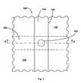
- FIG. 1is a plan view of an embodiment of a superconducting damascene interconnect, in accordance with the present invention.
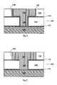
- FIG. 2is a partial cross-sectional view of one embodiment of a superconducting damascene interconnect, taken at line 2 — 2 of FIG. 1, in accordance with a first embodiment of the present invention.
- FIG. 3is a partial cross-sectional view of another embodiment of a superconducting damascene interconnect, taken at line 2 — 2 of FIG. 1, in accordance with a second embodiment of the present invention.
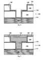
- FIG. 4is a partial cross-sectional view of a cavity for an interconnect formed in a dielectric, in accordance with the first embodiment of the present invention.
- FIG. 5is a partial cross-sectional view of a cavity for an interconnect formed in a dielectric, with a barrier layer deposited as a cavity liner, in accordance with the first embodiment of the present invention.
- FIG. 6is a partial cross-sectional view of a cavity for an interconnect formed in a dielectric, with a seed layer formed on a barrier layer, in accordance with the first embodiment of the present invention.
- FIG. 7is a partial cross-sectional view of a filled cavity for an interconnect formed in a dielectric, with a seed layer formed on a barrier layer, and the cavity filled with a superconductor precursor, in accordance with the first embodiment of the present invention.
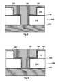
- FIG. 8is a partial cross-sectional view of a filled cavity for an interconnect, following an annealing step, with a barrier layer remaining, and with the cavity filled with a superconductor, in accordance with the first embodiment of the present invention.
- FIG. 9is a partial cross-sectional view of a another embodiment of a filled cavity for an interconnect, following an annealing step, with a barrier layer and a portion of a seed layer remaining, and with the cavity filled with a superconductor, in accordance with the first embodiment of the present invention.
- FIG. 10is a partial cross-sectional view of a cavity for an interconnect formed in a dielectric, with a first superconductor precursor layer deposited as a cavity liner, in accordance with a second embodiment of the present invention.
- FIG. 11is a partial cross-sectional view of a cavity for an interconnect formed in a dielectric, with a seed layer formed on a first superconductor precursor layer, in accordance with the second embodiment of the present invention.
- FIG. 12is a partial cross-sectional view of a filled cavity for an interconnect formed in a dielectric, with a seed layer formed on a first layer of a superconductor precursor, and the cavity filled with the superconductor precursor, in accordance with the second embodiment of the present invention.
- FIG. 13is a partial cross-sectional view of a filled cavity for an interconnect, following an annealing step, with the cavity filled with a superconductor, in accordance with the second embodiment of the present invention.
- FIG. 14is a flow diagram of a method of fabrication of a first embodiment of a superconductor damascene interconnect.
- FIG. 15is a flow diagram of a method of fabrication of a second embodiment of a superconductor damascene interconnect.
- the method of the present inventionmay be applied to a semiconductor device as a dual damascene or single damascene process.
- the processis applied as a dual damascene process, in which the same metal is used for vias and overlying interconnect lines, and both via and line dielectrics are deposited before trench formation and filling.
- viasare formed before deposition of a line dielectric and subsequent trench formation and filling to create interconnect lines.
- Vias and linesmay be formed from different dielectrics in single damascene processes. The same structure or different structures may be obtained by these processes.
- the method of the present inventionis described in terms of a dual damascene process. However, as will be understood by those of skill in the art, the method is applicable to a single damascene process.
- the term “damascene”refers to both a single damascene process and a dual damascene process.
- the term “cavity”may refer to either or both of a via or a channel for an interconnect, and any similar structure in which a damascene interconnect may be formed.
- the channelmay also be referred to as a trench before it is filled with a conductive material to form a channel.
- cavityit is understood that either or both of these terms may be intended.
- specific reference to either such term, or to other terms encompassed by the term cavityis intended, such structure will be specifically identified.
- the present inventionrelates to a semiconductor device including a damascene superconducting interconnect.
- the damascene superconducting interconnectis formed of a Y—Ba—Cu—O superconducting material.
- the Y—Ba—Cu—O superconducting materialhas a chemical formula YBa 2 Cu 3 O 7-x , wherein x ⁇ 0.5.
- FIG. 1therein is shown a plan view of a pair of aligned semiconductor damascene channels of a conductive material such as aluminum, copper, tungsten, polysilicon or, in the present invention, a superconductor material, disposed over a production semiconductor wafer 100 .
- a first damascene channel 102is shown disposed below a second damascene channel 104 which extends substantially perpendicular to the first channel 102 in the plan view.
- a round via 106connects the first and second damascene channels 102 and 104 and is a part of the second damascene channel 104 .
- the via 106is an integral part of the second damascene interconnect channel 104 , the via 106 and the second channel 104 being formed as a single structure.
- the first damascene channel 102comprises a first conductive material.
- the first conductive materialis the Y—Ba—Cu—O superconducting material in accordance with the present invention.
- the second damascene channel 104is formed by filling a second channel opening 108 disposed in a second channel dielectric layer 110 with a second conductive material.
- the second conductive materialis the Y—Ba—Cu—O superconducting material in accordance with the present invention.
- the first damascene channel 102may be disposed over active circuit elements such as, e.g., a polysilicon gate and a dielectric of a semiconductor device on an integrated circuit chip (not shown).
- the first and second damascene channels 102 and 104are in horizontal planes separated vertically by a stop nitride layer 112 , a via dielectric layer 114 , and a thin via nitride layer 116 .
- a stop nitride layer 112e.g., a polysilicon gate and a dielectric of a semiconductor device on an integrated circuit chip (not shown).
- the first and second damascene channels 102 and 104are in horizontal planes separated vertically by a stop nitride layer 112 , a via dielectric layer 114 , and a thin via nitride layer 116 .
- One or more of these layersmay be referred to as an interlevel dielectric.
- a barrier layer 120disposed around the second damascene channel 104 and the via 106 .
- the barrier layer 120separates the second channel 104 and the via 106 from the second channel dielectric layer 110 and the via dielectric layer 114 , respectively, and thus from the remainder of the semiconductor device 100 .
- the barrier layer 120provides insulation between the material of the second channel 104 and the via 106 and the second channel dielectric layer 110 and the via dielectric layer 114 , respectively.
- the barrier layer 120may act to prevent diffusion, migration or electromigration of metals such as copper from the channel 104 and the via 106 into the adjacent dielectric layers.
- the barrier layer 120may be formed from one or more of Ta, TaN, TaSiN, TiSiN, TiW, or WN or similar materials known in the art.
- the barrier materialsmay also include cobalt (Co), nickel (Ni), and palladium (Pd), molybdenum (Mo) and tungsten (W).
- the barriermay be formed of an alloy, for example, alloys such as NiW, NiTa, NiMo, CoW, CoTa, CoMo, PdW, PdTa, and PdMo.
- the barrier layer 120should be electrically conductive, so as to provide electrical connection between the second channel 104 and the underlying first channel 102 .
- the barrier layer 120may also promote adhesion of the Y—Ba—Cu—O superconductor material to the material of the adjacent dielectric materials.
- the first damascene channel 102may be disposed over active circuit elements such as, e.g., a polysilicon gate and a dielectric of a semiconductor device on an integrated circuit chip (not shown).
- the first and second damascene channels 102 and 104are in horizontal planes separated vertically by a stop nitride layer 112 , a via dielectric layer 114 , and a thin via nitride layer 116 .
- the cross-sectional area of the round via 106 of FIG. 1forms a cylindrical via when it is filled with the second conductive material.
- the semiconductor device 200does not require a barrier layer.
- the Y—Ba—Cu—O superconducting materialdoes not include species which may migrate, move or diffuse into the adjacent ILD.
- the adjacent ILDis formed of a material, such as a low-k dielectric material, which is not susceptible to migration, movement or diffusion of conductive atoms from the adjacent damascene interconnect or channel.
- each of the first damascene channel 102 and the second damascene channel 104 and the cylindrical via 106may comprise a superconductor material, as described more fully below.
- the embodiments shown in FIGS. 2 and 3may include a Y—Ba—Cu—O superconductor formed in either or both of the damascene channels 102 and 104 and the via 106 .
- both of the damascene channels 102 and 104 , and the via 106comprise a Y—Ba—Cu—O superconductor.
- damascene channels 102 , 104 and the via 106are formed of a Y—Ba—Cu—O superconductor having a formula YBa 2 Cu 3 O 7-x , wherein x ⁇ 0.5.
- the Y—Ba—Cu—O superconductorhas a high critical temperature, Tc.
- the Tcis about 60° K. to about 92° K.
- the Y—Ba—Cu—O superconductoris formed by a method which includes filling the cavity by first depositing a Y—Ba—Cu alloy and annealing the Y—Ba—Cu alloy in an oxygen flow to form the Y—Ba—Cu—O superconductor. This process is described in greater detail hereinbelow.
- the via dielectric layer 114 and the second channel dielectric layer 110are formed of a conventional dielectric material, such as silicon dioxide, silicon nitride, or silicon oxynitride.
- the via dielectric layer 114 and the second channel dielectric layer 110are formed of a low-k dielectric.
- a low-k dielectricis a dielectric material which exhibits a dielectric constant substantially less than conventional dielectric materials. Silicon dioxide has a dielectric constant, k, of about 3.9-4.0. Air has a dielectric constant of 1.
- a low-k dielectric materialhas a dielectric constant, k, in the range from about 1.1 to about 3.8.
- the low-k dielectric materialis a plastic-type polymer, which has a k value in the range of about 2.0 to about 3.5.
- the low-k dielectric materialis benzocyclobutane (“BCB”).
- BCBhas a dielectric constant of about 2.7.
- the low-k dielectric materialis a deposition type and/or spin-on type material having a fluorine component.
- fluorinemay be introduced into a standard dielectric deposition process or a standard spin-on process.
- low-k fluorine incorporated dielectric materialsinclude for example, fluorosilicate glass (FSG), silicon oxyfluoride (F x SiO y ), hydrogen silsesquioxane, fluorinated polysilicon, poly-phenylquinoxaline, polyquinoline, methysilsesquixane polymer, and fluoropolymide.
- the low-k dielectric materialmay be made by replacing silane (SiH 4 ) with SiF 4 in a standard film deposition, which results in the production of a low-k F type film in a deposition plasma reaction.
- the low-k materialmay also be formed by any deposition from a fluorine containing ambient (i.e., F-containing ambient) such that a fluorine concentration in the range of 3-20 atom percent is achieved. With F-based films, a k value in the range of 3.0-3.8 is achievable, either from a deposition type formation or a spin-on type formation.
- the low-k materialmay also be organic.
- exemplary organic low-k materialsinclude hydrogen silsesquioxane, fluorinated polyimide, poly-phenylquinoxaline, polyquinoline, and methysilsesquixanepolymer.
- Air-gap technologymay also be used to lower the dielectric constant, k, between superconducting interconnect structures. This technology may include removal of dielectric material between interconnect lines to form air gaps having a k value of 1.
- the present inventionrelates to a method of forming a superconducting damascene interconnect structure, including the steps of forming a cavity in an interlevel dielectric; forming a barrier layer in the cavity; forming a seed layer in the cavity over the barrier layer; filling the cavity by electrodepositing a Y—Ba—Cu alloy; and annealing in oxygen flow to form a Y—Ba—Cu—O superconductor on the barrier layer.
- FIG. 14is a process flow diagram of the steps of the method of this embodiment as outlined here.
- a semiconductor device 100is provided, as shown in Step S 1401 in FIG. 14 .
- the first channel 102 in a first channel oxide layer (not shown) above portions of a semiconductor device (not shown)is put down using a first damascene process over a production semiconductor wafer 100 .
- the damascene processis a photolithographic process which uses a mask to define a first channel opening (not shown) in the first channel oxide layer.
- the first channel openingis then filled with the optional adhesion, barrier, and conductive material.
- the stop nitride layer 112 , the via dielectric layer 114 , and the via nitride layer 116would be successively deposited on top of the conductive material in the first channel 102 and the first channel oxide layer using deposition techniques such as those described hereinbelow in more detail with respect to the second channel 104 .
- the basis for the cylindrical via 106was formed.
- the subsequent deposition of the second channel dielectric layer 110prepared the way for the second channel 104 to be perpendicular to the first channel 102 .
- the second damascene processis a photolithographic process which uses a mask to define the second channel opening 108 in the second channel dielectric layer 110 . Since the second damascene process uses an anisotropic etch of the dielectric material, the etch also forms the cylindrical via opening 106 down to the stop nitride layer 112 . The anisotropic oxide etch etches faster in the vertical direction of FIGS. 2 and 3 than in the horizontal direction. The nitride etch of the stop nitride layer 112 exposes a portion of the first channel conductive material 102 and completes the etching steps, as shown in FIG. 4 .
- the step of forming a cavity, such as the second channel 104 and the via 106 in an interlevel dielectric such as the second channel dielectric layer 110 and the via dielectric layer 114may be carried out by any method known in the art for forming such a cavity in a dielectric material.
- the present inventionis not limited to any particular method of cavity formation.
- the cavitymay be formed using photolithographic patterning processes and anisotropic dry etching processes. There are several variations of patterning/etching sequences which may be used to form the cavity.
- the second channel 104may be patterned and etched first, followed by patterning and etching of the via 106 .
- both upper and lower parts of the trenchmay be etched in one step.
- the thin barrier layer 120is deposited on the second channel dielectric layer 110 and the via dielectric layer 114 in the second channel opening 108 and the cylindrical via opening 106 .
- the materials from which the barrier layer 120 may be formedinclude those disclosed above, and any other equivalent material known in the art.
- the barrier layer 120is deposited directly onto the second channel dielectric layer 110 and the via dielectric layer 114 in the second channel opening 108 and the cylindrical via opening 106 , with no intervening materials.
- Various metal deposition techniquescan be used for the deposition of the barrier layer materials, such techniques include but are not limited to physical vapor deposition, chemical vapor deposition, electroless deposition, electroplating, ion-metal plasma (IMP), hollow cathode magnetron (HCM), sputtering, atomic layer deposition (ALD) or a combination thereof.
- IMPion-metal plasma
- HCMhollow cathode magnetron
- ALDatomic layer deposition
- the thickness of the barrier layeris from about 5 mn to about 50 nm. In another embodiment, the thickness of the barrier layer is from about 10 nm to about 30 nm.
- a seed layer 122is a formed over the barrier layer 120 .
- the seed layer 122may be a metal such as copper, copper-silver alloy, silver, or another highly conductive metal.
- the seed layer 122is copper.
- the seed layermay be a metal such as gold, palladium, platinum, or alloys of any of the above metals.
- the seed layerbecomes an integral, chemically-reacted part of the superconductor material during subsequent annealing steps, as described more fully below.
- a first portion of the seed layerbecomes an integral, chemically reacted part of the superconductor material during subsequent annealing steps, while a remaining portion does not so react and thereby retains its character substantially as deposited, as described more fully below.
- the seed layer 122may be deposited by any of the techniques noted above for deposition of the barrier layer 120 .
- the seed layer 122is deposited by electrodeposition.
- the seed layer 122is deposited by electroless deposition.
- the seed layer 122may be quite thin.
- the seed layer 122is deposited to a thickness of about 1 nm to about 50 nm.
- the seed layer 122is deposited to a thickness of about 5 nm to about 20 nm.
- the seed layer 122is deposited to a thickness of about 1 nm to about 5 mn.
- the seed layer 122is deposited directly onto the barrier layer 120 , with no intervening materials.
- a material 124 which will eventually form the superconductor materialis deposited into the second channel opening 104 and via opening 106 .
- the material 124is a Y—Ba—Cu alloy.
- the Y—Ba—Cu alloy layer 124is formed by laser ablation, CVD or sputtering.
- the Y—Ba—Cu alloy 124is deposited by electrodeposition.
- the Y—Ba—Cu alloy 124is deposited using other conventional metal deposition techniques, such as those identified above for deposition of the barrier layer 120 .
- the Y—Ba—Cu alloy 124In depositing the Y—Ba—Cu alloy 124 onto the seed layer 122 , which is in turn formed on the barrier layer 120 , the Y—Ba—Cu alloy 124 forms a layer over the surface of the semiconductor device 100 , as shown in FIG. 7 . In one embodiment, the Y—Ba—Cu alloy 124 is deposited directly onto the seed layer 122 , with no intervening materials.
- the semiconductor deviceis subjected to annealing in an oxygen flow, to form a Y—Ba—Cu—O superconductor material 126 from the Y—Ba—Cu layer 124 and at least a portion of the seed layer 122 .
- the annealing stepis carried out in an oxygen flow, in which the oxygen may be provided as ozone, O 3 , or as oxygen, O 2 .
- the ozonemay be generated in situ, or provided from an external source.
- the annealing temperaturemay be reduced as compared to when oxygen, O 2 , is used.
- the oxygen providedincludes at least a portion of the oxygen in the form of singlet oxygen, 1 O•.
- the singlet oxygenmay be generated from any known source, such as application of high energy, short wavelength UV radiation to a stream of oxygen.
- the annealing conditionsinclude exposure to the oxygen flow at temperatures in the range from about 400° C. to about 900° C. for periods of time ranging from about 10 minutes to about 1000 minutes.
- the annealing temperatureis in the range from about 500° C. to about 800° C., and in another from 600° C. to about 700° C.
- the annealing timeis in the range from about 90 minutes to about 600 minutes.
- the annealing timeis in the range from about 150 to about 450 minutes.
- the annealing timeis in the range from about 180 to about 420 minutes.
- the annealing timeis in the range from about 240 to about 360 minutes, and in one embodiment, from about 240 to about 300 minutes.
- the step of annealing in an oxygen flowconverts the Y—Ba—Cu alloy 124 and a portion of the seed layer 122 into a Y—Ba—Cu—O superconductor material 126 .
- the oxygen provided by the oxygen flowreacts with the Y—Ba—Cu alloy 124 and the seed layer 122 , to form the Y—Ba—Cu—O superconductor material 126 , as shown in FIG. 8 .
- the Y—Ba—Cu—O superconductor materialhas a formula YBa 2 Cu 3 O 7-x , wherein x ⁇ 0.5.
- the step of annealing in an oxygen flowconverts the Y—Ba—Cu alloy 124 and substantially all of the seed layer 122 into a Y—Ba—Cu—O superconductor material 126 , as shown in FIG. 8 .
- annealing in an oxygen flowconverts the Y—Ba—Cu alloy 124 and only a portion of the seed layer 122 into a Y—Ba—Cu—O superconductor material 126 , thus leaving a thin seed layer 122 between the superconductor material 126 and the barrier layer 120 , as shown in FIG. 9 .
- a chemical mechanical polishing processis used to complete the process by removing excess superconductor material 126 from the upper surface of the semiconductor wafer 100 , to obtain the semiconductor device shown in FIG. 2, in which the Y—Ba—Cu—O superconductor material 126 forms the second channel 104 .
- the same processmay be used to form the first channel 102 of a Y—Ba—Cu—O superconductor material by essentially the same steps as described herein, except that it may be unnecessary to form a via.
- a method of forming a superconducting damascene interconnect structureincluding the steps of forming a cavity in an interlevel dielectric; forming a Y—Ba—Cu alloy layer in the cavity; forming a seed layer in the cavity over the Y—Ba—Cu alloy layer; filling the cavity by electrodepositing a Y—Ba—Cu alloy fill; and annealing in oxygen flow to form a Y—Ba—Cu—O superconductor on the dielectric.
- Pertinent details of this method to fabricate the device shown in FIG. 3are set forth in the following, with reference to FIGS. 4, 10 - 13 and 15 .
- FIG. 15is a process flow diagram of the steps of the method of this embodiment as outlined here.
- Step S 1501 and S 1502 in FIG. 15are essentially the same as in the previously described embodiment.
- the semiconductor device 100is provided in Step S 1501 .
- the first channel 102 in a first channel oxide layer (not shown) above portions of a semiconductor device (not shown)is put down using a first damascene process over a production semiconductor wafer 100 .
- the damascene processis a photolithographic process which uses a mask to define a first channel opening (not shown) in the first channel oxide layer.
- the first channel openingis then filled with the optional adhesion, barrier, and conductive material.
- the stop nitride layer 112 , the via dielectric layer 114 , and the via nitride layer 116would be successively deposited on top of the conductive material in the first channel 102 and the first channel oxide layer using deposition techniques such as those described hereinabove and below in more detail with respect to the second channel 104 .
- the basis for the cylindrical via 106was formed.
- the subsequent deposition of the second channel dielectric layer 110prepared the way for the second channel 104 to be perpendicular to the first channel 102 .
- the second damascene processis a photolithographic process which uses a mask to define the second channel opening 108 in the second channel dielectric layer 110 . Since the second damascene process uses an anisotropic etch of the dielectric material, the etch also forms the cylindrical via opening 106 down to the stop nitride layer 112 . The anisotropic oxide etch etches faster in the vertical direction of FIGS. 2 and 3 than in the horizontal direction. The nitride etch of the stop nitride layer 112 exposes a portion of the first channel conductive material 102 and completes the etching steps, as shown in FIG. 4 .
- the step of forming a cavity, such as the second channel 104 and the via 106 in an interlevel dielectric such as the second channel dielectric layer 110 and the via dielectric layer 114may be carried out by any method known in the art for forming such a cavity in a dielectric material.
- the present inventionis not limited to any particular method of cavity formation.
- the steps of the second embodiment of the method of the present inventionhave been the same as in the first embodiment of the method, and the semiconductor device 100 has been the same.
- the methodsdiverge, and the semiconductor device is referred to as the semiconductor device 200 , since the structure is hereafter different from the semiconductor device 100 .
- a base Y—Ba—Cu alloy layer 128is deposited on the second channel dielectric layer 110 and the via dielectric layer 114 in the second channel opening 108 and the cylindrical via opening 106 in the semiconductor device 200 .
- the base Y—Ba—Cu alloy layer 128may be formed by a deposition method such as laser ablation, CVD or sputtering.
- the base Y—Ba—Cu alloy layer 128is deposited directly onto the second channel dielectric layer 110 and the via dielectric layer 114 in the second channel opening 108 and the cylindrical via opening 106 , with no intervening materials.
- Various metal deposition techniquescan be used for the deposition of the base Y—Ba—Cu alloy layer 128 , such techniques include but are not limited to physical vapor deposition, chemical vapor deposition, electroless deposition, electroplating, ion-metal plasma (IMP), hollow cathode magnetron (HCM), sputtering, atomic layer deposition (ALD) or a combination thereof.
- physical vapor depositionchemical vapor deposition
- electroless depositionelectroplating
- HCMhollow cathode magnetron
- sputteringatomic layer deposition (ALD) or a combination thereof.
- the thickness of the base Y—Ba—Cu alloy layer 128is from about 5 nm to about 50 nm. In another embodiment, the thickness of the barrier layer is from about 10 nm to about 30 mn.
- a seed layer 122is formed over the base Y—Ba—Cu alloy layer 128 of the semiconductor device 200 .
- the seed layer 122may be a metal such as copper, copper-silver alloy, silver, or other highly conductive metals.
- the seed layer 122is copper.
- the seed layer 122comprises copper, e.g., copper included in an alloy or a mixture.
- the seed layer 122is a copper-silver alloy, and in another embodiment, the seed layer 122 comprises silver.
- the seed layer 122may be or comprise a metal such as gold, palladium, platinum, or alloys of any of the above metals.
- the seed layer 122becomes an integral, chemically reacted part of the superconductor material during subsequent annealing steps, as described more fully below. In another embodiment, a portion of the seed layer 122 becomes an integral, chemically reacted part of the superconductor material during subsequent annealing steps, while a remaining portion of the seed layer 122 does not so react and thereby retains its character substantially as deposited, as described more fully below.
- the seed layer 122 in this embodimentmay be the same as or different from the seed layer 122 described above for the first embodiment.
- the seed layer 122may be deposited by any of the techniques noted above for deposition of the base Y—Ba—Cu alloy layer 128 . In one embodiment, the seed layer 122 is deposited by electrodeposition. The seed layer 122 may be quite thin. In one embodiment, the seed layer 122 is deposited to a thickness of about 1 nm to about 50 nm. In one embodiment, the seed layer 122 is deposited to a thickness of about 5 nm to about 20 nm. In another embodiment, the seed layer 122 is deposited to a thickness of about 1 nm to about 5 nm. In one embodiment, the seed layer 122 is deposited directly onto the barrier layer 120 , with no intervening materials.
- a material 124 which will eventually form the superconductor materialis deposited into and fills the second channel opening 104 and via opening 106 .
- the material 124is a Y—Ba—Cu alloy fill.
- the Y—Ba—Cu alloy fill 124is formed by laser ablation, CVD or sputtering.
- the Y—Ba—Cu alloy fill 124is deposited by electrodeposition.
- the Y—Ba—Cu alloy fill 124is deposited using other conventional metal deposition techniques, such as those identified above for deposition of the barrier layer 120 .
- the Y—Ba—Cu alloy fill 124In depositing the Y—Ba—Cu alloy fill 124 onto the seed layer 122 and filling the channel 104 , the Y—Ba—Cu alloy fill 124 forms a layer over the surface of the semiconductor device 100 , as shown in FIG. 12 . In one embodiment, the Y—Ba—Cu alloy fill 124 is deposited directly onto the seed layer 122 , with no intervening materials.
- the semiconductor device 200is subjected to annealing in an oxygen flow, to form a second Y—Ba—Cu—superconductor material 130 from the Y—Ba—Cu alloy fill 124 , the base Y—Ba—Cu alloy layer 128 and the seed layer 122 .
- the annealing stepis carried out in an oxygen flow, in which the oxygen is provided as ozone, O 3 , or as oxygen, O 2 .
- the ozonemay be generated in situ, or provided from an external source.
- the oxygen providedincludes at least a portion of the oxygen in the form of singlet oxygen, 1 O•.
- the singlet oxygenmay be generated from any known source, such as application of high energy, short wavelength UV radiation to a stream of oxygen.
- the annealing conditionsinclude exposure to the oxygen at temperatures in the range from about 400° C. to about 900° C. for periods of time ranging from about 10 minutes to about 1000 minutes.
- the annealing temperatureis in the range from about 500° C. to about 800° C., and in another from 600° C. to about 700° C.
- the annealing timeis in the range from about 30 minutes to about 150 minutes.
- the step of annealing in an oxygen flowconverts the Y—Ba—Cu alloy fill 124 , the base Y—Ba—Cu alloy layer 128 and the seed layer 122 into a second Y—Ba—Cu—O superconductor material 130 .
- the oxygen provided by the oxygen flowreacts with the Y—Ba—Cu alloy fill 124 , the base Y—Ba—Cu alloy layer 128 and the seed layer 122 , to form the Y—Ba—Cu—O superconductor material 130 , as shown in FIG. 13 .
- the Y—Ba—Cu—O superconductor materialhas a formula YBa 2 Cu 3 O 7-x , wherein x ⁇ 0.5.
- the step of annealing in an oxygen flowconverts the Y—Ba—Cu alloy fill 124 , the base Y—Ba—Cu alloy layer 128 and substantially all of the seed layer 122 into a Y—Ba—Cu—O superconductor material 130 , as shown in FIG. 13 .
- a chemical mechanical polishing processis used to complete the process by removing excess second superconductor material 130 from the upper surface of the semiconductor wafer 100 , to obtain the semiconductor device shown in FIG. 3, in which the Y—Ba—Cu—O superconductor material 130 forms the second channel 104 , and in which no barrier layer remains between the Y—Ba—Cu—O superconductor material 130 and the adjacent dielectric materials.
- the same processcould be used to form the first channel 102 of a Y—Ba—Cu—O superconductor material by essentially the same steps as described herein.
Landscapes
- Physics & Mathematics (AREA)
- Condensed Matter Physics & Semiconductors (AREA)
- General Physics & Mathematics (AREA)
- Engineering & Computer Science (AREA)
- Computer Hardware Design (AREA)
- Microelectronics & Electronic Packaging (AREA)
- Power Engineering (AREA)
- Internal Circuitry In Semiconductor Integrated Circuit Devices (AREA)
Abstract
Description
The present invention relates to a semiconductor device comprising a superconductor damascene interconnect, and a method of manufacturing the semiconductor device. The invention has particular applicability in manufacturing high density semiconductor devices with deep submicron design features which require low RLC delay interconnections between active devices.
Current demands for high density and performance associated with ultra large scale integration (ULSI) require submicron features of significantly less than 0.25 microns, increased transistor and circuit speeds and improved reliability. As feature size decreases, the sizes of the resulting transistors as well as those of the interconnects between transistors also decrease. Fabrication of smaller transistors allows more transistors to be placed on a single monolithic substrate, thereby allowing relatively large circuit systems to be incorporated on a single, relatively small die area. This trend toward reduced feature sizes imposes severe demands on many aspects of IC fabrication, including interconnect formation. In the manufacture of integrated circuits, after the individual devices, such as the transistors, have been fabricated in the silicon substrate, they must be connected together to perform the desired circuit functions. The connections are commonly referred to as interconnects. Narrower interconnects have reduced cross-sectional area, which results in a higher interconnect resistance for a given interconnect material. This interconnect resistance, along with the capacitance of the interconnect with respect to ground and other interconnects, contributes to an RLC (resistive-inductive-capacitive) time constant which characterizes delays associated with propagation along the interconnect line. Fabrication of a circuit with increased RLC time constants lowers the speed at which the circuit can operate by increasing the time needed, for example, for a circuit output voltage to respond to a change in input voltage. Although there are other parasitic resistances and capacitances in an integrated circuit, such as those associated with the transistors themselves, in modem circuits having submicron feature sizes interconnects may contribute as much as 80% of the total circuit delay time. The increased interconnect resistance described above places a limit on how narrow interconnect lines can be and maintain tolerable interconnect resistance. The greater the resistivity of the interconnect material, the wider the lines must be, as discussed further below. As feature size decreases and transistor density increases, multiple layers of interconnect must be used to connect the transistors to each other and to the terminals of the integrated circuit. The limitation discussed above on the narrowness of interconnect lines can exacerbate this need for multiple interconnect layers. Fabrication of each interconnect layer requires deposition and patterning processes, adding to the expense of the circuit and increasing the opportunity for defect incorporation and the resulting yield reduction. It is therefore desirable to minimize the number of interconnect layers required.
Lowering the resistivity of the interconnect material alleviates many of the interconnect-related problems discussed above. Resistance, R, along the length of a structure formed from a given material is related to the resistivity, ρ, of the material by R=ρl/A, where 1 is the length of the structure and A is its cross-sectional area. It can therefore be seen that lowering the resistivity of an interconnect material reduces the resistance of an interconnect line of a given cross-sectional area. Furthermore, a line formed from a lower-resistivity material could be made narrower before an unacceptable resistance level is reached than a line formed from a higher-resistivity material. This ability to form narrower lines may allow fewer interconnect levels to be used to form the required connections for an IC, thereby reducing costs and potentially increasing the yield of correctly-functioning circuits.
Advantages such as those described above of low-resistivity interconnect materials have driven a movement in the semiconductor industry toward replacing aluminum interconnects with interconnects made from copper. The resistivity of pure copper (about 1.7μΩ·cm) is significantly lower than that of pure aluminum (about 2.6μΩ·cm). Both aluminum and copper interconnects typically contain small concentrations of other elements to improve interconnect reliability. These added elements increase the resistivity of the metal, but practical copper interconnects still have resistivities up to 40% lower than those of practical aluminum interconnects. Copper interconnects can therefore be made narrower than aluminum interconnects for a given value of interconnect resistance. This may result in fewer levels of metallization being needed with copper interconnects. For a given interconnect cross-sectional area, copper interconnects exhibit lower resistances, and therefore shorter interconnect-related delays, than do aluminum interconnects.
Because copper is more difficult to etch than aluminum, in addition to difficulties in etching narrow features in metals in general as compared to etching of insulators, copper interconnects are generally formed by a damascene process.
In one connection process, which is called a “dual damascene” technique, two channels of conductive materials, are positioned in vertically separated planes perpendicular to each other and interconnected by a vertical “via” at their closest point.
The first channel part of the dual damascene process starts with the placement of a first channel dielectric layer, which is typically an oxide layer, over the semiconductor devices. A first damascene step photoresist is then placed over the oxide layer and is photolithographically processed to form the pattern of the first channels. An anisotropic oxide etch is then used to etch out the channel oxide layer to form the first channel openings. The damascene step photoresist is stripped and an optional thin adhesion layer is deposited to coat the walls of the first channel opening to ensure good adhesion and electrical contact of subsequent layers to the underlying semiconductor devices. A barrier layer is then deposited on the adhesion layer improve the formation of subsequently deposited conductive material and to act as a barrier material to prevent diffusion of such conductive material into the oxide layer and the semiconductor devices. A first conductive material is then deposited and subjected to a chemical-mechanical polishing process which removes the first conductive material above the first channel oxide layer and damascenes the first conductive material in the first channel openings to form the first channels.
The via formation step of the dual damascene process starts with the deposition of a thin stop nitride over the first channel and the first channel oxide layer. Subsequently, a separating oxide layer is deposited on the stop nitride. This is followed by deposition of a thin via nitride. Then a via step photoresist is used in a photolithographic process to designate round via areas over the first channels.
A nitride etch is then used to etch out the round via areas in the via nitride. The via step photoresist is then removed, or stripped. A second channel dielectric layer, which is typically an oxide layer, is then deposited over the via nitride and the exposed oxide in the via area of the via nitride. A second damascene step photoresist is placed over the second channel oxide layer and is photolithographically processed to form the pattern of the second channels. An anisotropic oxide etch is then used to etch the second channel oxide layer to form the second channel openings and, during the same etching process to etch the via areas down to the thin stop nitride layer above the first channels to form the via openings. The damascene photoresist is then removed, and a nitride etch process removes the nitride above the first channels in the via areas. An adhesion layer is then deposited to coat the via openings and the second channel openings. Next, a barrier layer is deposited on the adhesion layer. This is followed by a deposition of the second conductive material in the second channel openings and the via openings to form the second channel and the via. A second chemical mechanical polishing process leaves the two vertically separated, horizontally perpendicular channels connected by cylindrical vias.
The use of the dual damascene technique eliminates metal etch and dielectric gap fill steps typically used in the metallization process. The elimination of metal etch steps is important as the semiconductor industry moves from aluminum to other metallization materials, such as copper, which are very difficult to etch.
Improvements in circuit speed gained by moving from aluminum to copper have been quite beneficial as circuit speeds have increased by moving the working frequency into the range of about 1 GHz. However, development of integrated circuits having a working frequency in the range from 5 to 50 GHz requires even lower RLC delay interconnections than can be provided by copper. Thus, there exists a need semiconductor devices having interconnections having an RLC delay significantly lower than that provided by copper.
The present invention relates to a superconducting damascene interconnect structure for a semiconductor device, and to a method for fabricating the superconducting damascene interconnect structure. Thus, the present invention solves the problem of providing a significantly reduced RLC delay interconnection by replacing the conventional damascene interconnect materials with a superconductor. In addition, the present invention relates to a method of fabricating the superconducting damascene interconnect structure by a series of steps which are simple and conventional, but which avoid known problems associated with formation of damascene interconnects.
Thus, the present invention provides a method of forming a superconducting damascene interconnect structure, including:
forming a cavity in an interlevel dielectric;
forming a barrier layer in the cavity;
forming a seed layer in the cavity over the barrier layer;
filling the cavity by electrodepositing a Y—Ba—Cu alloy; and
annealing in oxygen flow to form a Y—Ba—Cu—O superconductor on the barrier layer. In one embodiment, the Y—Ba—Cu—O superconductor has a formula YBa2Cu3O7-x, wherein x≦0.5.
In another embodiment, the present invention relates to a method of forming a superconducting damascene interconnect structure, including:
forming a cavity in an interlevel dielectric;
forming a Y—Ba—Cu alloy layer in the cavity;
forming a seed layer in the cavity over the Y—Ba—Cu alloy layer;
filling the cavity by electrodepositing a Y—Ba—Cu alloy fill; and
annealing in oxygen flow to form a Y—Ba—Cu—O superconductor on the dielectric.
In another embodiment, the present invention relates to a damascene interconnect in a semiconductor device, including a Y—Ba—Cu—O superconductor formed in a cavity in a dielectric material. In one embodiment, the Y—Ba—Cu—O superconductor has a formula YBa2Cu3O7-x, wherein x≦0.5.
Thus, the present invention provides a solution to the problem of providing semiconductor devices having interconnections having an RLC delay significantly lower than that provided by copper. The present invention provides a method for making a device, and a device, having a working frequency in the range from 5 to 50 GHz, which results in lower RLC delay interconnections than can be provided by copper.
FIG. 1, is a plan view of an embodiment of a superconducting damascene interconnect, in accordance with the present invention.
FIG. 2 is a partial cross-sectional view of one embodiment of a superconducting damascene interconnect, taken at line2—2 of FIG. 1, in accordance with a first embodiment of the present invention.
FIG. 3 is a partial cross-sectional view of another embodiment of a superconducting damascene interconnect, taken at line2—2 of FIG. 1, in accordance with a second embodiment of the present invention.
FIG. 4 is a partial cross-sectional view of a cavity for an interconnect formed in a dielectric, in accordance with the first embodiment of the present invention.
FIG. 5 is a partial cross-sectional view of a cavity for an interconnect formed in a dielectric, with a barrier layer deposited as a cavity liner, in accordance with the first embodiment of the present invention.
FIG. 6 is a partial cross-sectional view of a cavity for an interconnect formed in a dielectric, with a seed layer formed on a barrier layer, in accordance with the first embodiment of the present invention.
FIG. 7 is a partial cross-sectional view of a filled cavity for an interconnect formed in a dielectric, with a seed layer formed on a barrier layer, and the cavity filled with a superconductor precursor, in accordance with the first embodiment of the present invention.
FIG. 8 is a partial cross-sectional view of a filled cavity for an interconnect, following an annealing step, with a barrier layer remaining, and with the cavity filled with a superconductor, in accordance with the first embodiment of the present invention.
FIG. 9 is a partial cross-sectional view of a another embodiment of a filled cavity for an interconnect, following an annealing step, with a barrier layer and a portion of a seed layer remaining, and with the cavity filled with a superconductor, in accordance with the first embodiment of the present invention.
FIG. 10 is a partial cross-sectional view of a cavity for an interconnect formed in a dielectric, with a first superconductor precursor layer deposited as a cavity liner, in accordance with a second embodiment of the present invention.
FIG. 11 is a partial cross-sectional view of a cavity for an interconnect formed in a dielectric, with a seed layer formed on a first superconductor precursor layer, in accordance with the second embodiment of the present invention.
FIG. 12 is a partial cross-sectional view of a filled cavity for an interconnect formed in a dielectric, with a seed layer formed on a first layer of a superconductor precursor, and the cavity filled with the superconductor precursor, in accordance with the second embodiment of the present invention.
FIG. 13 is a partial cross-sectional view of a filled cavity for an interconnect, following an annealing step, with the cavity filled with a superconductor, in accordance with the second embodiment of the present invention.
FIG. 14 is a flow diagram of a method of fabrication of a first embodiment of a superconductor damascene interconnect.
FIG. 15 is a flow diagram of a method of fabrication of a second embodiment of a superconductor damascene interconnect.
The method of the present invention may be applied to a semiconductor device as a dual damascene or single damascene process. In one embodiment, the process is applied as a dual damascene process, in which the same metal is used for vias and overlying interconnect lines, and both via and line dielectrics are deposited before trench formation and filling. In a single damascene process, vias are formed before deposition of a line dielectric and subsequent trench formation and filling to create interconnect lines. Vias and lines may be formed from different dielectrics in single damascene processes. The same structure or different structures may be obtained by these processes. The method of the present invention is described in terms of a dual damascene process. However, as will be understood by those of skill in the art, the method is applicable to a single damascene process. Thus, as used herein, the term “damascene” refers to both a single damascene process and a dual damascene process.
As used herein, the term “cavity” may refer to either or both of a via or a channel for an interconnect, and any similar structure in which a damascene interconnect may be formed. The channel may also be referred to as a trench before it is filled with a conductive material to form a channel. Thus, when the term “cavity” is used, it is understood that either or both of these terms may be intended. When specific reference to either such term, or to other terms encompassed by the term cavity is intended, such structure will be specifically identified.
In a first embodiment, the present invention relates to a semiconductor device including a damascene superconducting interconnect. In one embodiment, the damascene superconducting interconnect is formed of a Y—Ba—Cu—O superconducting material. In one embodiment, the Y—Ba—Cu—O superconducting material has a chemical formula YBa2Cu3O7-x, wherein x≦0.5.
Referring first to FIG. 1, therein is shown a plan view of a pair of aligned semiconductor damascene channels of a conductive material such as aluminum, copper, tungsten, polysilicon or, in the present invention, a superconductor material, disposed over aproduction semiconductor wafer 100. A firstdamascene channel 102 is shown disposed below a seconddamascene channel 104 which extends substantially perpendicular to thefirst channel 102 in the plan view. Similarly, a round via106 connects the first and seconddamascene channels damascene channel 104. In one embodiment, the via106 is an integral part of the seconddamascene interconnect channel 104, the via106 and thesecond channel 104 being formed as a single structure. The firstdamascene channel 102 comprises a first conductive material. In one embodiment, the first conductive material is the Y—Ba—Cu—O superconducting material in accordance with the present invention. The seconddamascene channel 104 is formed by filling a second channel opening108 disposed in a secondchannel dielectric layer 110 with a second conductive material. In one embodiment, the second conductive material is the Y—Ba—Cu—O superconducting material in accordance with the present invention.
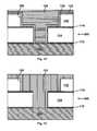
Referring now to FIG. 2, therein is shown a cross-section, taken along a line2—2 in FIG. 1, of asemiconductor device 100 in accordance with a first embodiment of the present invention. The firstdamascene channel 102 may be disposed over active circuit elements such as, e.g., a polysilicon gate and a dielectric of a semiconductor device on an integrated circuit chip (not shown). The first and seconddamascene channels stop nitride layer 112, a viadielectric layer 114, and a thin vianitride layer 116. One or more of these layers may be referred to as an interlevel dielectric. The cross-sectional area of the round via106 of FIG. 1 forms a cylindrical via when it is filled with the second conductive material.
Also shown in thesemiconductor device 100 of the embodiment of FIG. 2, disposed around the seconddamascene channel 104 and the via106, is abarrier layer 120. Thebarrier layer 120 separates thesecond channel 104 and the via106 from the secondchannel dielectric layer 110 and the viadielectric layer 114, respectively, and thus from the remainder of thesemiconductor device 100. Thebarrier layer 120 provides insulation between the material of thesecond channel 104 and the via106 and the secondchannel dielectric layer 110 and the viadielectric layer 114, respectively. Thebarrier layer 120 may act to prevent diffusion, migration or electromigration of metals such as copper from thechannel 104 and the via106 into the adjacent dielectric layers.
Thebarrier layer 120 may be formed from one or more of Ta, TaN, TaSiN, TiSiN, TiW, or WN or similar materials known in the art. The barrier materials may also include cobalt (Co), nickel (Ni), and palladium (Pd), molybdenum (Mo) and tungsten (W). The barrier may be formed of an alloy, for example, alloys such as NiW, NiTa, NiMo, CoW, CoTa, CoMo, PdW, PdTa, and PdMo.
Thebarrier layer 120 should be electrically conductive, so as to provide electrical connection between thesecond channel 104 and the underlyingfirst channel 102. Thebarrier layer 120 may also promote adhesion of the Y—Ba—Cu—O superconductor material to the material of the adjacent dielectric materials.
Referring now to FIG. 3, therein is shown a cross-section, taken along a line2—2 in FIG. 1, of asemiconductor device 200 in accordance with a second embodiment of the present invention. This embodiment is similar to the embodiment of FIG. 2 except that it does not include a barrier layer. As in the first embodiment, in the second embodiment, the firstdamascene channel 102 may be disposed over active circuit elements such as, e.g., a polysilicon gate and a dielectric of a semiconductor device on an integrated circuit chip (not shown). The first and seconddamascene channels stop nitride layer 112, a viadielectric layer 114, and a thin vianitride layer 116. The cross-sectional area of the round via106 of FIG. 1 forms a cylindrical via when it is filled with the second conductive material.
In the second embodiment, shown in FIG. 3, thesemiconductor device 200 does not require a barrier layer. In one embodiment, the Y—Ba—Cu—O superconducting material does not include species which may migrate, move or diffuse into the adjacent ILD. In one embodiment, the adjacent ILD is formed of a material, such as a low-k dielectric material, which is not susceptible to migration, movement or diffusion of conductive atoms from the adjacent damascene interconnect or channel.
In the embodiments shown in FIGS. 2 and 3, each of the firstdamascene channel 102 and the seconddamascene channel 104 and the cylindrical via106 may comprise a superconductor material, as described more fully below. The embodiments shown in FIGS. 2 and 3 may include a Y—Ba—Cu—O superconductor formed in either or both of thedamascene channels via 106. In one embodiment, both of thedamascene channels
In one embodiment,damascene channels
In one embodiment, the viadielectric layer 114 and the secondchannel dielectric layer 110 are formed of a conventional dielectric material, such as silicon dioxide, silicon nitride, or silicon oxynitride. In another embodiment, the viadielectric layer 114 and the secondchannel dielectric layer 110 are formed of a low-k dielectric. A low-k dielectric is a dielectric material which exhibits a dielectric constant substantially less than conventional dielectric materials. Silicon dioxide has a dielectric constant, k, of about 3.9-4.0. Air has a dielectric constant of 1. A low-k dielectric material has a dielectric constant, k, in the range from about 1.1 to about 3.8. In one embodiment, the low-k dielectric material is a plastic-type polymer, which has a k value in the range of about 2.0 to about 3.5. In one embodiment, the low-k dielectric material is benzocyclobutane (“BCB”). BCB has a dielectric constant of about 2.7. In another embodiment, the low-k dielectric material is a deposition type and/or spin-on type material having a fluorine component.
With respect to the low-k dielectric materials having a fluorine component, fluorine may be introduced into a standard dielectric deposition process or a standard spin-on process. Examples of low-k fluorine incorporated dielectric materials include for example, fluorosilicate glass (FSG), silicon oxyfluoride (FxSiOy), hydrogen silsesquioxane, fluorinated polysilicon, poly-phenylquinoxaline, polyquinoline, methysilsesquixane polymer, and fluoropolymide. The low-k dielectric material may be made by replacing silane (SiH4) with SiF4in a standard film deposition, which results in the production of a low-k F type film in a deposition plasma reaction. The low-k material may also be formed by any deposition from a fluorine containing ambient (i.e., F-containing ambient) such that a fluorine concentration in the range of 3-20 atom percent is achieved. With F-based films, a k value in the range of 3.0-3.8 is achievable, either from a deposition type formation or a spin-on type formation.
The low-k material may also be organic. Exemplary organic low-k materials include hydrogen silsesquioxane, fluorinated polyimide, poly-phenylquinoxaline, polyquinoline, and methysilsesquixanepolymer.
Air-gap technology may also be used to lower the dielectric constant, k, between superconducting interconnect structures. This technology may include removal of dielectric material between interconnect lines to form air gaps having a k value of 1.
In one embodiment, the present invention relates to a method of forming a superconducting damascene interconnect structure, including the steps of forming a cavity in an interlevel dielectric; forming a barrier layer in the cavity; forming a seed layer in the cavity over the barrier layer; filling the cavity by electrodepositing a Y—Ba—Cu alloy; and annealing in oxygen flow to form a Y—Ba—Cu—O superconductor on the barrier layer. Pertinent details of this method to fabricate the device shown in FIG. 2 are set forth in the following, with reference to FIGS. 4-9 and14. FIG. 14 is a process flow diagram of the steps of the method of this embodiment as outlined here.
As the first step of the method, asemiconductor device 100 is provided, as shown in Step S1401 in FIG.14. Included in this step, thefirst channel 102 in a first channel oxide layer (not shown) above portions of a semiconductor device (not shown) is put down using a first damascene process over aproduction semiconductor wafer 100. The damascene process is a photolithographic process which uses a mask to define a first channel opening (not shown) in the first channel oxide layer. The first channel opening is then filled with the optional adhesion, barrier, and conductive material. Thestop nitride layer 112, the viadielectric layer 114, and the vianitride layer 116 would be successively deposited on top of the conductive material in thefirst channel 102 and the first channel oxide layer using deposition techniques such as those described hereinbelow in more detail with respect to thesecond channel 104.
Referring to FIG. 4, by using the via photoresist and the via photolithographic process followed by nitride etching of a round viaopening 106 in the vianitride layer 116, the basis for the cylindrical via106 was formed. The subsequent deposition of the secondchannel dielectric layer 110 prepared the way for thesecond channel 104 to be perpendicular to thefirst channel 102.
As shown in FIG.4 and as Step S1402 in FIG. 14, a cavity forming thechannel 104 and the via106 is formed next. The second damascene process is a photolithographic process which uses a mask to define the second channel opening108 in the secondchannel dielectric layer 110. Since the second damascene process uses an anisotropic etch of the dielectric material, the etch also forms the cylindrical via opening106 down to thestop nitride layer 112. The anisotropic oxide etch etches faster in the vertical direction of FIGS. 2 and 3 than in the horizontal direction. The nitride etch of thestop nitride layer 112 exposes a portion of the first channelconductive material 102 and completes the etching steps, as shown in FIG.4.
The step of forming a cavity, such as thesecond channel 104 and the via106 in an interlevel dielectric such as the secondchannel dielectric layer 110 and the viadielectric layer 114 may be carried out by any method known in the art for forming such a cavity in a dielectric material. The present invention is not limited to any particular method of cavity formation. The cavity may be formed using photolithographic patterning processes and anisotropic dry etching processes. There are several variations of patterning/etching sequences which may be used to form the cavity. For example, thesecond channel 104 may be patterned and etched first, followed by patterning and etching of thevia 106. Alternatively, with appropriate patterning, both upper and lower parts of the trench may be etched in one step.
Thereafter, as shown in FIG.5 and as Step S1403 in FIG. 14, thethin barrier layer 120 is deposited on the secondchannel dielectric layer 110 and the viadielectric layer 114 in thesecond channel opening 108 and the cylindrical viaopening 106. The materials from which thebarrier layer 120 may be formed include those disclosed above, and any other equivalent material known in the art. In one embodiment, thebarrier layer 120 is deposited directly onto the secondchannel dielectric layer 110 and the viadielectric layer 114 in thesecond channel opening 108 and the cylindrical viaopening 106, with no intervening materials.
Various metal deposition techniques can be used for the deposition of the barrier layer materials, such techniques include but are not limited to physical vapor deposition, chemical vapor deposition, electroless deposition, electroplating, ion-metal plasma (IMP), hollow cathode magnetron (HCM), sputtering, atomic layer deposition (ALD) or a combination thereof.
In one embodiment, the thickness of the barrier layer is from about 5 mn to about 50 nm. In another embodiment, the thickness of the barrier layer is from about 10 nm to about 30 nm.
Next, as shown in FIG.6 and as Step S1404 in FIG. 14, aseed layer 122 is a formed over thebarrier layer 120. Theseed layer 122 may be a metal such as copper, copper-silver alloy, silver, or another highly conductive metal. In one embodiment, theseed layer 122 is copper. In one embodiment, a copper-silver alloy, and in another embodiment, silver. In other embodiments, the seed layer may be a metal such as gold, palladium, platinum, or alloys of any of the above metals. In one embodiment, the seed layer becomes an integral, chemically-reacted part of the superconductor material during subsequent annealing steps, as described more fully below. In another embodiment, a first portion of the seed layer becomes an integral, chemically reacted part of the superconductor material during subsequent annealing steps, while a remaining portion does not so react and thereby retains its character substantially as deposited, as described more fully below.
Theseed layer 122 may be deposited by any of the techniques noted above for deposition of thebarrier layer 120. In one embodiment, theseed layer 122 is deposited by electrodeposition. In one embodiment, theseed layer 122 is deposited by electroless deposition. Theseed layer 122 may be quite thin. In one embodiment, theseed layer 122 is deposited to a thickness of about 1 nm to about 50 nm. In one embodiment, theseed layer 122 is deposited to a thickness of about 5 nm to about 20 nm. In another embodiment, theseed layer 122 is deposited to a thickness of about 1 nm to about 5 mn. In one embodiment, theseed layer 122 is deposited directly onto thebarrier layer 120, with no intervening materials.
Next, as shown in FIG.7 and as Step S1405 in FIG. 14, amaterial 124 which will eventually form the superconductor material is deposited into thesecond channel opening 104 and viaopening 106. In one embodiment, thematerial 124 is a Y—Ba—Cu alloy. In one embodiment, the Y—Ba—Cu alloy layer 124 is formed by laser ablation, CVD or sputtering. In another embodiment, the Y—Ba—Cu alloy 124 is deposited by electrodeposition. In other embodiments, the Y—Ba—Cu alloy 124 is deposited using other conventional metal deposition techniques, such as those identified above for deposition of thebarrier layer 120.
In depositing the Y—Ba—Cu alloy 124 onto theseed layer 122, which is in turn formed on thebarrier layer 120, the Y—Ba—Cu alloy 124 forms a layer over the surface of thesemiconductor device 100, as shown in FIG.7. In one embodiment, the Y—Ba—Cu alloy 124 is deposited directly onto theseed layer 122, with no intervening materials.
As shown in FIGS. 8 and 9, with the Y—Ba—Cu layer 124 in place in thesecond channel 104 and the via106, the semiconductor device is subjected to annealing in an oxygen flow, to form a Y—Ba—Cu—O superconductor material 126 from the Y—Ba—Cu layer 124 and at least a portion of theseed layer 122.
The annealing step is carried out in an oxygen flow, in which the oxygen may be provided as ozone, O3, or as oxygen, O2. The ozone may be generated in situ, or provided from an external source. In an embodiment in which ozone, O3, is provided as the source of oxygen flow, the annealing temperature may be reduced as compared to when oxygen, O2, is used. In one embodiment, the oxygen provided includes at least a portion of the oxygen in the form of singlet oxygen,1O•. The singlet oxygen may be generated from any known source, such as application of high energy, short wavelength UV radiation to a stream of oxygen.
The annealing conditions include exposure to the oxygen flow at temperatures in the range from about 400° C. to about 900° C. for periods of time ranging from about 10 minutes to about 1000 minutes. In one embodiment, the annealing temperature is in the range from about 500° C. to about 800° C., and in another from 600° C. to about 700° C. In one embodiment, the annealing time is in the range from about 90 minutes to about 600 minutes. In one embodiment, the annealing time is in the range from about 150 to about 450 minutes. In another embodiment, the annealing time is in the range from about 180 to about 420 minutes. In another embodiment, the annealing time is in the range from about 240 to about 360 minutes, and in one embodiment, from about 240 to about 300 minutes. With respect to all rates, ratios and ranges disclosed herein, the limits of the rates, ratios and ranges may be combined or interchanged.
The step of annealing in an oxygen flow converts the Y—Ba—Cu alloy 124 and a portion of theseed layer 122 into a Y—Ba—Cu—O superconductor material 126. In the annealing step, the oxygen provided by the oxygen flow reacts with the Y—Ba—Cu alloy 124 and theseed layer 122, to form the Y—Ba—Cu—O superconductor material 126, as shown in FIG.8. In one embodiment, the Y—Ba—Cu—O superconductor material has a formula YBa2Cu3O7-x, wherein x≦0.5.
In one embodiment, the step of annealing in an oxygen flow converts the Y—Ba—Cu alloy 124 and substantially all of theseed layer 122 into a Y—Ba—Cu—O superconductor material 126, as shown in FIG.8. In another embodiment, annealing in an oxygen flow converts the Y—Ba—Cu alloy 124 and only a portion of theseed layer 122 into a Y—Ba—Cu—O superconductor material 126, thus leaving athin seed layer 122 between thesuperconductor material 126 and thebarrier layer 120, as shown in FIG.9.
Thereafter, a chemical mechanical polishing process is used to complete the process by removingexcess superconductor material 126 from the upper surface of thesemiconductor wafer 100, to obtain the semiconductor device shown in FIG. 2, in which the Y—Ba—Cu—O superconductor material 126 forms thesecond channel 104.
As noted above, although not separately described, the same process may be used to form thefirst channel 102 of a Y—Ba—Cu—O superconductor material by essentially the same steps as described herein, except that it may be unnecessary to form a via.
A method of forming a superconducting damascene interconnect structure, including the steps of forming a cavity in an interlevel dielectric; forming a Y—Ba—Cu alloy layer in the cavity; forming a seed layer in the cavity over the Y—Ba—Cu alloy layer; filling the cavity by electrodepositing a Y—Ba—Cu alloy fill; and annealing in oxygen flow to form a Y—Ba—Cu—O superconductor on the dielectric. Pertinent details of this method to fabricate the device shown in FIG. 3 are set forth in the following, with reference to FIGS. 4,10-13 and15. FIG. 15 is a process flow diagram of the steps of the method of this embodiment as outlined here.
In this embodiment, the initial steps, shown as Steps S1501 and S1502 in FIG. 15, are essentially the same as in the previously described embodiment. Thesemiconductor device 100 is provided in Step S1501. Thefirst channel 102 in a first channel oxide layer (not shown) above portions of a semiconductor device (not shown) is put down using a first damascene process over aproduction semiconductor wafer 100. The damascene process is a photolithographic process which uses a mask to define a first channel opening (not shown) in the first channel oxide layer. The first channel opening is then filled with the optional adhesion, barrier, and conductive material. Thestop nitride layer 112, the viadielectric layer 114, and the vianitride layer 116 would be successively deposited on top of the conductive material in thefirst channel 102 and the first channel oxide layer using deposition techniques such as those described hereinabove and below in more detail with respect to thesecond channel 104.
Referring to FIG. 4, by using the via photoresist and the via photolithographic process followed by nitride etching of a round viaopening 106 in the vianitride layer 116, the basis for the cylindrical via106 was formed. The subsequent deposition of the secondchannel dielectric layer 110 prepared the way for thesecond channel 104 to be perpendicular to thefirst channel 102.
As shown in FIG.4 and in Step S1502 of FIG. 15, the cavity forming thechannel 104 and the via106 is formed next. The second damascene process is a photolithographic process which uses a mask to define the second channel opening108 in the secondchannel dielectric layer 110. Since the second damascene process uses an anisotropic etch of the dielectric material, the etch also forms the cylindrical via opening106 down to thestop nitride layer 112. The anisotropic oxide etch etches faster in the vertical direction of FIGS. 2 and 3 than in the horizontal direction. The nitride etch of thestop nitride layer 112 exposes a portion of the first channelconductive material 102 and completes the etching steps, as shown in FIG.4.
As noted above, the step of forming a cavity, such as thesecond channel 104 and the via106 in an interlevel dielectric such as the secondchannel dielectric layer 110 and the viadielectric layer 114 may be carried out by any method known in the art for forming such a cavity in a dielectric material. The present invention is not limited to any particular method of cavity formation.
Up to this point, the steps of the second embodiment of the method of the present invention have been the same as in the first embodiment of the method, and thesemiconductor device 100 has been the same. Hereafter, the methods diverge, and the semiconductor device is referred to as thesemiconductor device 200, since the structure is hereafter different from thesemiconductor device 100.
Next, as shown in FIG.10 and in Step S1503 of FIG. 15, a base Y—Ba—Cu alloy layer 128 is deposited on the secondchannel dielectric layer 110 and the viadielectric layer 114 in thesecond channel opening 108 and the cylindrical via opening106 in thesemiconductor device 200. The base Y—Ba—Cu alloy layer 128 may be formed by a deposition method such as laser ablation, CVD or sputtering. In one embodiment, the base Y—Ba—Cu alloy layer 128 is deposited directly onto the secondchannel dielectric layer 110 and the viadielectric layer 114 in thesecond channel opening 108 and the cylindrical viaopening 106, with no intervening materials.
Various metal deposition techniques can be used for the deposition of the base Y—Ba—Cu alloy layer 128, such techniques include but are not limited to physical vapor deposition, chemical vapor deposition, electroless deposition, electroplating, ion-metal plasma (IMP), hollow cathode magnetron (HCM), sputtering, atomic layer deposition (ALD) or a combination thereof.
In one embodiment, the thickness of the base Y—Ba—Cu alloy layer 128 is from about 5 nm to about 50 nm. In another embodiment, the thickness of the barrier layer is from about 10 nm to about 30 mn.
Next, as shown in FIG.11 and in Step S1504 of FIG. 15, aseed layer 122 is formed over the base Y—Ba—Cu alloy layer 128 of thesemiconductor device 200. Theseed layer 122 may be a metal such as copper, copper-silver alloy, silver, or other highly conductive metals. In one embodiment, theseed layer 122 is copper. In one embodiment, theseed layer 122 comprises copper, e.g., copper included in an alloy or a mixture. In one embodiment, theseed layer 122 is a copper-silver alloy, and in another embodiment, theseed layer 122 comprises silver. In other embodiments, theseed layer 122 may be or comprise a metal such as gold, palladium, platinum, or alloys of any of the above metals. In one embodiment, theseed layer 122 becomes an integral, chemically reacted part of the superconductor material during subsequent annealing steps, as described more fully below. In another embodiment, a portion of theseed layer 122 becomes an integral, chemically reacted part of the superconductor material during subsequent annealing steps, while a remaining portion of theseed layer 122 does not so react and thereby retains its character substantially as deposited, as described more fully below. Theseed layer 122 in this embodiment may be the same as or different from theseed layer 122 described above for the first embodiment.
Theseed layer 122 may be deposited by any of the techniques noted above for deposition of the base Y—Ba—Cu alloy layer 128. In one embodiment, theseed layer 122 is deposited by electrodeposition. Theseed layer 122 may be quite thin. In one embodiment, theseed layer 122 is deposited to a thickness of about 1 nm to about 50 nm. In one embodiment, theseed layer 122 is deposited to a thickness of about 5 nm to about 20 nm. In another embodiment, theseed layer 122 is deposited to a thickness of about 1 nm to about 5 nm. In one embodiment, theseed layer 122 is deposited directly onto thebarrier layer 120, with no intervening materials.
Next, as shown in FIG.12 and as Step S1505 in FIG. 15, amaterial 124 which will eventually form the superconductor material is deposited into and fills thesecond channel opening 104 and viaopening 106. In one embodiment, thematerial 124 is a Y—Ba—Cu alloy fill. In one embodiment, the Y—Ba—Cu alloy fill124 is formed by laser ablation, CVD or sputtering. In another embodiment, the Y—Ba—Cu alloy fill124 is deposited by electrodeposition. In other embodiments, the Y—Ba—Cu alloy fill124 is deposited using other conventional metal deposition techniques, such as those identified above for deposition of thebarrier layer 120.
In depositing the Y—Ba—Cu alloy fill124 onto theseed layer 122 and filling thechannel 104, the Y—Ba—Cu alloy fill124 forms a layer over the surface of thesemiconductor device 100, as shown in FIG.12. In one embodiment, the Y—Ba—Cu alloy fill124 is deposited directly onto theseed layer 122, with no intervening materials.
As shown in FIG. 13, with the Y—Ba—Cu alloy fill124 in place in thesecond channel 104 and the via106, thesemiconductor device 200 is subjected to annealing in an oxygen flow, to form a second Y—Ba—Cu—superconductor material 130 from the Y—Ba—Cu alloy fill124, the base Y—Ba—Cu alloy layer 128 and theseed layer 122. The annealing step is carried out in an oxygen flow, in which the oxygen is provided as ozone, O3, or as oxygen, O2. The ozone may be generated in situ, or provided from an external source. In one embodiment, the oxygen provided includes at least a portion of the oxygen in the form of singlet oxygen,1O•. The singlet oxygen may be generated from any known source, such as application of high energy, short wavelength UV radiation to a stream of oxygen.
The annealing conditions include exposure to the oxygen at temperatures in the range from about 400° C. to about 900° C. for periods of time ranging from about 10 minutes to about 1000 minutes. In one embodiment, the annealing temperature is in the range from about 500° C. to about 800° C., and in another from 600° C. to about 700° C. In one embodiment, the annealing time is in the range from about 30 minutes to about 150 minutes.
The step of annealing in an oxygen flow converts the Y—Ba—Cu alloy fill124, the base Y—Ba—Cu alloy layer 128 and theseed layer 122 into a second Y—Ba—Cu—O superconductor material 130. In the annealing step, the oxygen provided by the oxygen flow reacts with the Y—Ba—Cu alloy fill124, the base Y—Ba—Cu alloy layer 128 and theseed layer 122, to form the Y—Ba—Cu—O superconductor material 130, as shown in FIG.13. In one embodiment, the Y—Ba—Cu—O superconductor material has a formula YBa2Cu3O7-x, wherein x≦0.5.
In this embodiment, the step of annealing in an oxygen flow converts the Y—Ba—Cu alloy fill124, the base Y—Ba—Cu alloy layer 128 and substantially all of theseed layer 122 into a Y—Ba—Cu—O superconductor material 130, as shown in FIG.13.
Thereafter, a chemical mechanical polishing process is used to complete the process by removing excesssecond superconductor material 130 from the upper surface of thesemiconductor wafer 100, to obtain the semiconductor device shown in FIG. 3, in which the Y—Ba—Cu—O superconductor material 130 forms thesecond channel 104, and in which no barrier layer remains between the Y—Ba—Cu—O superconductor material 130 and the adjacent dielectric materials.
As noted above, although not separately described, the same process could be used to form thefirst channel 102 of a Y—Ba—Cu—O superconductor material by essentially the same steps as described herein.
What has been described above are certain embodiments of the present invention. It is, of course, not possible to describe every conceivable combination of components or methodologies for purposes of describing the present invention, but one of ordinary skill in the art will recognize that many further combinations and permutations of the present invention are possible. Accordingly, the present invention is intended to embrace all such alterations, modifications and variations that fall within the spirit and scope of the appended claims.
Claims (20)
1. A method of forming a superconducting damascene interconnect structure, comprising:
forming a cavity in an interlevel dielectric;
forming a barrier layer in the cavity;
forming a seed layer in the cavity over the barrier layer;
filling the cavity by electrodepositing a Y—Ba—Cu alloy; and
annealing in oxygen flow to form a Y—Ba—Cu—O superconductor on the barrier layer.
2. The method ofclaim 1 , wherein the barrier layer comprises one or more of Ta, TaN, TaSiN, TiSiN, WN, Co, Ni, Pd, Mo, W, NiW, NiTa, NiMo, CoW, CoTa, CoMo, PdW, PdTa, and PdMo.
3. The method ofclaim 2 , wherein the barrier layer is formed by CVD, PVD, HCM, electroless, electroplating, IMP, sputtering, or ALD.
4. The method ofclaim 1 , wherein the seed layer is formed from Cu, a Cu—Ag alloy or Ag.
5. The method ofclaim 4 , wherein the seed layer is formed by electrodeposition or electroless deposition.
6. The method ofclaim 1 , wherein the Y—Ba—Cu layer is formed by laser ablation, CVD or sputtering.
7. The method ofclaim 1 , wherein the step of annealing forms the Y—Ba—Cu—O superconductor from the seed layer and the Y—Ba—Cu layer.
8. The method ofclaim 1 , wherein the Y—Ba—Cu—O superconductor has a formula YBa2Cu3d7-x, wherein x≦0.5.
9. A method of forming a superconducting damascene interconnect structure, comprising:
forming a cavity in an interlevel dielectric;
forming a Y—Ba—Cu alloy layer in the cavity;
forming a seed layer in the cavity over the Y—Ba—Cu alloy layer;
filling the cavity by electrodepositing a Y—Ba—Cu alloy fill; and
annealing in oxygen flow to form a Y—Ba—Cu—O superconductor on the dielectric.
10. The method ofclaim 9 , wherein the Y—Ba—Cu alloy layer is formed by laser ablation, CVD or sputtering.
11. The method ofclaim 10 , wherein the seed layer is formed from Cu, a Cu—Ag alloy or Ag.
12. The method ofclaim 11 , wherein the seed layer is formed by electrodeposition or electroless deposition.
13. The method ofclaim 10 , wherein the step of annealing forms the Y—Ba—Cu—O superconductor from the Y—Ba—Cu alloy layer, the seed layer, and the Y—Ba—Cu alloy fill.
14. The method ofclaim 1 , wherein the Y—Ba—Cu—O superconductor has a formula YBa2Cu3O7-x, wherein x≦0.5.
15. A damascene interconnect in a semiconductor device, comprising a Y—Ba—Cu—O superconductor formed in a cavity in a dielectric material.
16. The superconductor damascene interconnect ofclaim 15 , wherein the damascene interconnect is in electrical contact with a second interconnect.
17. The superconductor damascene interconnect ofclaim 15 , wherein the cavity further comprises a barrier layer between the interconnect and the cavity.
18. The superconductor damascene interconnect ofclaim 17 , wherein the barrier layer comprises one or more of Ta, TaN, TaSiN, TiSiN, WN, Co, Ni, Pd, Mo, W, NiW, NiTa, NiMo, CoW, CoTa, CoMo, PdW, PdTa, and PdMo.
19. The superconductor damascene interconnect ofclaim 17 , wherein the cavity further comprises a seed layer between the interconnect and the barrier layer.
20. The superconductor damascene interconnect ofclaim 15 , wherein the Y—Ba—Cu—O superconductor has a formula YBa2Cu3O7-x, wherein x≦0.5.
Priority Applications (1)
| Application Number | Priority Date | Filing Date | Title |
|---|---|---|---|
| US09/844,845US6420189B1 (en) | 2001-04-27 | 2001-04-27 | Superconducting damascene interconnected for integrated circuit |
Applications Claiming Priority (1)
| Application Number | Priority Date | Filing Date | Title |
|---|---|---|---|
| US09/844,845US6420189B1 (en) | 2001-04-27 | 2001-04-27 | Superconducting damascene interconnected for integrated circuit |
Publications (1)
| Publication Number | Publication Date |
|---|---|
| US6420189B1true US6420189B1 (en) | 2002-07-16 |
Family
ID=25293778
Family Applications (1)
| Application Number | Title | Priority Date | Filing Date |
|---|---|---|---|
| US09/844,845Expired - Fee RelatedUS6420189B1 (en) | 2001-04-27 | 2001-04-27 | Superconducting damascene interconnected for integrated circuit |
Country Status (1)
| Country | Link |
|---|---|
| US (1) | US6420189B1 (en) |
Cited By (86)
| Publication number | Priority date | Publication date | Assignee | Title |
|---|---|---|---|---|
| US20020197863A1 (en)* | 2001-06-20 | 2002-12-26 | Mak Alfred W. | System and method to form a composite film stack utilizing sequential deposition techniques |
| US20030104126A1 (en)* | 2001-10-10 | 2003-06-05 | Hongbin Fang | Method for depositing refractory metal layers employing sequential deposition techniques |
| US20030186524A1 (en)* | 2002-04-01 | 2003-10-02 | Hynix Semiconductor Inc. | Method of forming metal interconnection layer in semiconductor device |
| US20030190497A1 (en)* | 2002-04-08 | 2003-10-09 | Applied Materials, Inc. | Cyclical deposition of a variable content titanium silicon nitride layer |
| US20030232497A1 (en)* | 2002-04-16 | 2003-12-18 | Ming Xi | System and method for forming an integrated barrier layer |
| US20040014315A1 (en)* | 2001-07-16 | 2004-01-22 | Applied Materials, Inc. | Formation of composite tungsten films |
| US6809026B2 (en) | 2001-12-21 | 2004-10-26 | Applied Materials, Inc. | Selective deposition of a barrier layer on a metal film |
| US20040227243A1 (en)* | 2003-05-15 | 2004-11-18 | Dung-Ching Perng | Methods of pore sealing and metal encapsulation in porous low k interconnect |
| US6821563B2 (en) | 2002-10-02 | 2004-11-23 | Applied Materials, Inc. | Gas distribution system for cyclical layer deposition |
| US6827978B2 (en) | 2002-02-11 | 2004-12-07 | Applied Materials, Inc. | Deposition of tungsten films |
| US6831004B2 (en) | 2000-06-27 | 2004-12-14 | Applied Materials, Inc. | Formation of boride barrier layers using chemisorption techniques |
| US6833161B2 (en) | 2002-02-26 | 2004-12-21 | Applied Materials, Inc. | Cyclical deposition of tungsten nitride for metal oxide gate electrode |
| US6838125B2 (en) | 2002-07-10 | 2005-01-04 | Applied Materials, Inc. | Method of film deposition using activated precursor gases |
| US6846516B2 (en) | 2002-04-08 | 2005-01-25 | Applied Materials, Inc. | Multiple precursor cyclical deposition system |
| US20050020060A1 (en)* | 2002-01-29 | 2005-01-27 | Titta Aaltonen | Process for producing metal thin films by ALD |
| US6855368B1 (en) | 2000-06-28 | 2005-02-15 | Applied Materials, Inc. | Method and system for controlling the presence of fluorine in refractory metal layers |
| US20050077627A1 (en)* | 2003-10-10 | 2005-04-14 | Chen-Hua Yu | Copper wiring with high temperature superconductor (HTS) layer |
| US6916398B2 (en) | 2001-10-26 | 2005-07-12 | Applied Materials, Inc. | Gas delivery apparatus and method for atomic layer deposition |
| US6936538B2 (en) | 2001-07-16 | 2005-08-30 | Applied Materials, Inc. | Method and apparatus for depositing tungsten after surface treatment to improve film characteristics |
| US20050255706A1 (en)* | 2004-05-12 | 2005-11-17 | Sanyo Electric Co., Ltd. | Method for manufacturing semiconductor device |
| US20060006538A1 (en)* | 2004-07-02 | 2006-01-12 | Lsi Logic Corporation | Extreme low-K interconnect structure and method |
| US6998014B2 (en) | 2002-01-26 | 2006-02-14 | Applied Materials, Inc. | Apparatus and method for plasma assisted deposition |
| US7049226B2 (en) | 2001-09-26 | 2006-05-23 | Applied Materials, Inc. | Integration of ALD tantalum nitride for copper metallization |
| US7077860B2 (en) | 1997-04-24 | 2006-07-18 | Advanced Cardiovascular Systems, Inc. | Method of reducing or eliminating thrombus formation |
| US7094685B2 (en) | 2002-01-26 | 2006-08-22 | Applied Materials, Inc. | Integration of titanium and titanium nitride layers |
| US20060264031A1 (en)* | 2000-06-28 | 2006-11-23 | Ming Xi | Method for depositing tungsten-containing layers by vapor deposition techniques |
| US20070026654A1 (en)* | 2005-03-15 | 2007-02-01 | Hannu Huotari | Systems and methods for avoiding base address collisions |
| US7198675B2 (en) | 2003-09-30 | 2007-04-03 | Advanced Cardiovascular Systems | Stent mandrel fixture and method for selectively coating surfaces of a stent |
| US7211144B2 (en) | 2001-07-13 | 2007-05-01 | Applied Materials, Inc. | Pulsed nucleation deposition of tungsten layers |
| US7211508B2 (en) | 2003-06-18 | 2007-05-01 | Applied Materials, Inc. | Atomic layer deposition of tantalum based barrier materials |
| US7258891B2 (en) | 2001-06-28 | 2007-08-21 | Advanced Cardiovascular Systems, Inc. | Stent mounting assembly and a method of using the same to coat a stent |
| US7262133B2 (en) | 2003-01-07 | 2007-08-28 | Applied Materials, Inc. | Enhancement of copper line reliability using thin ALD tan film to cap the copper line |
| CN100336219C (en)* | 2002-12-04 | 2007-09-05 | 国际商业机器公司 | Structure comprising a barrier layer of a tungsten alloy and manufacturing method thereof |
| US20070257369A1 (en)* | 2006-05-08 | 2007-11-08 | Taiwan Semiconductor Manufacturing Company, Ltd. | Reducing resistivity in interconnect structures of integrated circuits |
| US7297159B2 (en) | 2000-10-26 | 2007-11-20 | Advanced Cardiovascular Systems, Inc. | Selective coating of medical devices |
| US20070298608A1 (en)* | 2002-10-31 | 2007-12-27 | Johnston Steven W | Forming a copper diffusion barrier |
| US20080012133A1 (en)* | 2006-07-13 | 2008-01-17 | Taiwan Semiconductor Manufacturing Company, Ltd. | Reducing resistivity in interconnect structures by forming an inter-layer |
| US7405158B2 (en) | 2000-06-28 | 2008-07-29 | Applied Materials, Inc. | Methods for depositing tungsten layers employing atomic layer deposition techniques |
| US7416979B2 (en) | 2001-07-25 | 2008-08-26 | Applied Materials, Inc. | Deposition methods for barrier and tungsten materials |
| US7429402B2 (en) | 2004-12-10 | 2008-09-30 | Applied Materials, Inc. | Ruthenium as an underlayer for tungsten film deposition |
| US20080286965A1 (en)* | 2007-05-14 | 2008-11-20 | Hsien-Ming Lee | Novel approach for reducing copper line resistivity |
| KR100873017B1 (en)* | 2002-07-19 | 2008-12-09 | 주식회사 하이닉스반도체 | Formation method of multilayer metal wiring |
| US7470611B2 (en) | 1998-10-01 | 2008-12-30 | Applied Materials, Inc. | In situ deposition of a low K dielectric layer, barrier layer, etch stop, and anti-reflective coating for damascene application |
| US7494908B2 (en) | 2001-09-26 | 2009-02-24 | Applied Materials, Inc. | Apparatus for integration of barrier layer and seed layer |
| US20090155997A1 (en)* | 2007-12-12 | 2009-06-18 | Asm Japan K.K. | METHOD FOR FORMING Ta-Ru LINER LAYER FOR Cu WIRING |
| US7553377B1 (en) | 2004-04-27 | 2009-06-30 | Advanced Cardiovascular Systems, Inc. | Apparatus and method for electrostatic coating of an abluminal stent surface |
| US7563324B1 (en) | 2003-12-29 | 2009-07-21 | Advanced Cardiovascular Systems Inc. | System and method for coating an implantable medical device |
| US7611990B2 (en) | 2001-07-25 | 2009-11-03 | Applied Materials, Inc. | Deposition methods for barrier and tungsten materials |
| US7632307B2 (en) | 2004-12-16 | 2009-12-15 | Advanced Cardiovascular Systems, Inc. | Abluminal, multilayer coating constructs for drug-delivery stents |
| US7682946B2 (en) | 2005-11-04 | 2010-03-23 | Applied Materials, Inc. | Apparatus and process for plasma-enhanced atomic layer deposition |
| US7732327B2 (en) | 2000-06-28 | 2010-06-08 | Applied Materials, Inc. | Vapor deposition of tungsten materials |
| US20100171220A1 (en)* | 2006-05-08 | 2010-07-08 | Taiwan Semiconductor Manufacturing Company, Ltd. | Reducing Resistivity in Interconnect Structures of Integrated Circuits |
| US7780785B2 (en) | 2001-10-26 | 2010-08-24 | Applied Materials, Inc. | Gas delivery apparatus for atomic layer deposition |
| US7799674B2 (en) | 2008-02-19 | 2010-09-21 | Asm Japan K.K. | Ruthenium alloy film for copper interconnects |
| US7867547B2 (en) | 2005-12-19 | 2011-01-11 | Advanced Cardiovascular Systems, Inc. | Selectively coating luminal surfaces of stents |
| US7955979B2 (en) | 2000-05-15 | 2011-06-07 | Asm International N.V. | Method of growing electrical conductors |
| US7964505B2 (en) | 2005-01-19 | 2011-06-21 | Applied Materials, Inc. | Atomic layer deposition of tungsten materials |
| CN102117796A (en)* | 2011-01-28 | 2011-07-06 | 复旦大学 | Copper interconnection structure of integrated circuit and preparation method thereof |
| US8003156B2 (en) | 2006-05-04 | 2011-08-23 | Advanced Cardiovascular Systems, Inc. | Rotatable support elements for stents |
| US8017237B2 (en) | 2006-06-23 | 2011-09-13 | Abbott Cardiovascular Systems, Inc. | Nanoshells on polymers |
| US8025922B2 (en) | 2005-03-15 | 2011-09-27 | Asm International N.V. | Enhanced deposition of noble metals |
| US8048441B2 (en) | 2007-06-25 | 2011-11-01 | Abbott Cardiovascular Systems, Inc. | Nanobead releasing medical devices |
| US8048448B2 (en) | 2006-06-15 | 2011-11-01 | Abbott Cardiovascular Systems Inc. | Nanoshells for drug delivery |
| US8084104B2 (en) | 2008-08-29 | 2011-12-27 | Asm Japan K.K. | Atomic composition controlled ruthenium alloy film formed by plasma-enhanced atomic layer deposition |
| US8110489B2 (en) | 2001-07-25 | 2012-02-07 | Applied Materials, Inc. | Process for forming cobalt-containing materials |
| US8133555B2 (en) | 2008-10-14 | 2012-03-13 | Asm Japan K.K. | Method for forming metal film by ALD using beta-diketone metal complex |
| US8187970B2 (en) | 2001-07-25 | 2012-05-29 | Applied Materials, Inc. | Process for forming cobalt and cobalt silicide materials in tungsten contact applications |
| US8273408B2 (en) | 2007-10-17 | 2012-09-25 | Asm Genitech Korea Ltd. | Methods of depositing a ruthenium film |
| US8329569B2 (en) | 2009-07-31 | 2012-12-11 | Asm America, Inc. | Deposition of ruthenium or ruthenium dioxide |
| US8603530B2 (en) | 2006-06-14 | 2013-12-10 | Abbott Cardiovascular Systems Inc. | Nanoshell therapy |
| US20140159145A1 (en)* | 2012-12-06 | 2014-06-12 | Samsung Electronics Co., Ltd. | Semiconductor device |
| US9051641B2 (en) | 2001-07-25 | 2015-06-09 | Applied Materials, Inc. | Cobalt deposition on barrier surfaces |
| US20150235953A1 (en)* | 2014-02-14 | 2015-08-20 | Taiwan Semiconductor Manufacturing Company Limited | Semiconductor device and formation thereof |
| US9129897B2 (en) | 2008-12-19 | 2015-09-08 | Asm International N.V. | Metal silicide, metal germanide, methods for making the same |
| US9379011B2 (en) | 2008-12-19 | 2016-06-28 | Asm International N.V. | Methods for depositing nickel films and for making nickel silicide and nickel germanide |
| US20160276156A1 (en)* | 2015-03-16 | 2016-09-22 | Taiwan Semiconductor Manufacturing Company Ltd. | Semiconductor device and manufacturing process thereof |
| US9607842B1 (en) | 2015-10-02 | 2017-03-28 | Asm Ip Holding B.V. | Methods of forming metal silicides |
| US9754943B1 (en) | 2016-09-21 | 2017-09-05 | United Microelectronics Corp. | Dynamic random access memory device |
| US11856871B2 (en) | 2018-11-13 | 2023-12-26 | D-Wave Systems Inc. | Quantum processors |
| US11930721B2 (en) | 2012-03-08 | 2024-03-12 | 1372934 B.C. Ltd. | Systems and methods for fabrication of superconducting integrated circuits |
| US11957065B2 (en) | 2017-02-01 | 2024-04-09 | 1372934 B.C. Ltd. | Systems and methods for fabrication of superconducting integrated circuits |
| US12102017B2 (en) | 2019-02-15 | 2024-09-24 | D-Wave Systems Inc. | Kinetic inductance for couplers and compact qubits |
| US12354877B2 (en) | 2020-06-24 | 2025-07-08 | Asm Ip Holding B.V. | Vapor deposition of films comprising molybdenum |
| US12367412B2 (en) | 2019-12-05 | 2025-07-22 | 1372934 B.C. Ltd. | Systems and methods for fabricating flux trap mitigating superconducting integrated circuits |
| US12376501B2 (en) | 2020-05-11 | 2025-07-29 | 1372934 B.C. Ltd. | Kinetic inductance devices, methods for fabricating kinetic inductance devices, and articles employing the same |
| US12392823B2 (en) | 2021-11-05 | 2025-08-19 | D-Wave Systems Inc. | Systems and methods for on-chip noise measurements |
Citations (19)
| Publication number | Priority date | Publication date | Assignee | Title |
|---|---|---|---|---|
| US5183800A (en)* | 1987-07-15 | 1993-02-02 | Sharp Kabushiki Kaisha | Interconnection method for semiconductor device comprising a high-temperature superconductive material |
| US5439780A (en) | 1992-04-29 | 1995-08-08 | At&T Corp. | Energy sensitive materials and methods for their use |
| US5593918A (en)* | 1994-04-22 | 1997-01-14 | Lsi Logic Corporation | Techniques for forming superconductive lines |
| US5659201A (en) | 1995-06-05 | 1997-08-19 | Advanced Micro Devices, Inc. | High conductivity interconnection line |
| US5811375A (en) | 1991-12-02 | 1998-09-22 | Sumitomo Electric Industries Ltd. | Superconducting multilayer interconnection formed of oxide superconductor material and method for manufacturing the same |
| US5900668A (en) | 1995-11-30 | 1999-05-04 | Advanced Micro Devices, Inc. | Low capacitance interconnection |
| US6016000A (en)* | 1998-04-22 | 2000-01-18 | Cvc, Inc. | Ultra high-speed chip semiconductor integrated circuit interconnect structure and fabrication method using free-space dielectrics |
| US6042998A (en) | 1993-09-30 | 2000-03-28 | The University Of New Mexico | Method and apparatus for extending spatial frequencies in photolithography images |
| US6071809A (en) | 1998-09-25 | 2000-06-06 | Rockwell Semiconductor Systems, Inc. | Methods for forming high-performing dual-damascene interconnect structures |
| US6083842A (en) | 1999-02-19 | 2000-07-04 | Advanced Micro Devices Inc. | Fabrication of a via plug having high aspect ratio with a diffusion barrier layer effectively surrounding the via plug |
| US6096641A (en) | 1999-01-19 | 2000-08-01 | Mitsubishi Denki Kabushiki Kaisha | Method of manufacturing semiconductor device |
| US6103624A (en) | 1999-04-15 | 2000-08-15 | Advanced Micro Devices, Inc. | Method of improving Cu damascene interconnect reliability by laser anneal before barrier polish |
| US6124198A (en)* | 1998-04-22 | 2000-09-26 | Cvc, Inc. | Ultra high-speed chip interconnect using free-space dielectrics |
| US6127263A (en) | 1998-07-10 | 2000-10-03 | Applied Materials, Inc. | Misalignment tolerant techniques for dual damascene fabrication |
| US6133051A (en) | 1998-06-30 | 2000-10-17 | Advanced Technology Materials, Inc. | Amorphously deposited metal oxide ceramic films |
| US6144099A (en) | 1999-03-30 | 2000-11-07 | Advanced Micro Devices, Inc. | Semiconductor metalization barrier |
| US6144096A (en) | 1998-10-05 | 2000-11-07 | Advanced Micro Devices, Inc. | Low resistivity semiconductor barrier layers and manufacturing method therefor |
| US6157081A (en) | 1999-03-10 | 2000-12-05 | Advanced Micro Devices, Inc. | High-reliability damascene interconnect formation for semiconductor fabrication |
| US6174799B1 (en) | 1999-01-05 | 2001-01-16 | Advanced Micro Devices, Inc. | Graded compound seed layers for semiconductors |
- 2001
- 2001-04-27USUS09/844,845patent/US6420189B1/ennot_activeExpired - Fee Related
Patent Citations (19)
| Publication number | Priority date | Publication date | Assignee | Title |
|---|---|---|---|---|
| US5183800A (en)* | 1987-07-15 | 1993-02-02 | Sharp Kabushiki Kaisha | Interconnection method for semiconductor device comprising a high-temperature superconductive material |
| US5811375A (en) | 1991-12-02 | 1998-09-22 | Sumitomo Electric Industries Ltd. | Superconducting multilayer interconnection formed of oxide superconductor material and method for manufacturing the same |
| US5439780A (en) | 1992-04-29 | 1995-08-08 | At&T Corp. | Energy sensitive materials and methods for their use |
| US6042998A (en) | 1993-09-30 | 2000-03-28 | The University Of New Mexico | Method and apparatus for extending spatial frequencies in photolithography images |
| US5593918A (en)* | 1994-04-22 | 1997-01-14 | Lsi Logic Corporation | Techniques for forming superconductive lines |
| US5659201A (en) | 1995-06-05 | 1997-08-19 | Advanced Micro Devices, Inc. | High conductivity interconnection line |
| US5900668A (en) | 1995-11-30 | 1999-05-04 | Advanced Micro Devices, Inc. | Low capacitance interconnection |
| US6124198A (en)* | 1998-04-22 | 2000-09-26 | Cvc, Inc. | Ultra high-speed chip interconnect using free-space dielectrics |
| US6016000A (en)* | 1998-04-22 | 2000-01-18 | Cvc, Inc. | Ultra high-speed chip semiconductor integrated circuit interconnect structure and fabrication method using free-space dielectrics |
| US6133051A (en) | 1998-06-30 | 2000-10-17 | Advanced Technology Materials, Inc. | Amorphously deposited metal oxide ceramic films |
| US6127263A (en) | 1998-07-10 | 2000-10-03 | Applied Materials, Inc. | Misalignment tolerant techniques for dual damascene fabrication |
| US6071809A (en) | 1998-09-25 | 2000-06-06 | Rockwell Semiconductor Systems, Inc. | Methods for forming high-performing dual-damascene interconnect structures |
| US6144096A (en) | 1998-10-05 | 2000-11-07 | Advanced Micro Devices, Inc. | Low resistivity semiconductor barrier layers and manufacturing method therefor |
| US6174799B1 (en) | 1999-01-05 | 2001-01-16 | Advanced Micro Devices, Inc. | Graded compound seed layers for semiconductors |
| US6096641A (en) | 1999-01-19 | 2000-08-01 | Mitsubishi Denki Kabushiki Kaisha | Method of manufacturing semiconductor device |
| US6083842A (en) | 1999-02-19 | 2000-07-04 | Advanced Micro Devices Inc. | Fabrication of a via plug having high aspect ratio with a diffusion barrier layer effectively surrounding the via plug |
| US6157081A (en) | 1999-03-10 | 2000-12-05 | Advanced Micro Devices, Inc. | High-reliability damascene interconnect formation for semiconductor fabrication |
| US6144099A (en) | 1999-03-30 | 2000-11-07 | Advanced Micro Devices, Inc. | Semiconductor metalization barrier |
| US6103624A (en) | 1999-04-15 | 2000-08-15 | Advanced Micro Devices, Inc. | Method of improving Cu damascene interconnect reliability by laser anneal before barrier polish |
Cited By (166)
| Publication number | Priority date | Publication date | Assignee | Title |
|---|---|---|---|---|
| US7077860B2 (en) | 1997-04-24 | 2006-07-18 | Advanced Cardiovascular Systems, Inc. | Method of reducing or eliminating thrombus formation |
| US7470611B2 (en) | 1998-10-01 | 2008-12-30 | Applied Materials, Inc. | In situ deposition of a low K dielectric layer, barrier layer, etch stop, and anti-reflective coating for damascene application |
| US7670945B2 (en) | 1998-10-01 | 2010-03-02 | Applied Materials, Inc. | In situ deposition of a low κ dielectric layer, barrier layer, etch stop, and anti-reflective coating for damascene application |
| US7955979B2 (en) | 2000-05-15 | 2011-06-07 | Asm International N.V. | Method of growing electrical conductors |
| US8536058B2 (en) | 2000-05-15 | 2013-09-17 | Asm International N.V. | Method of growing electrical conductors |
| US7501344B2 (en) | 2000-06-27 | 2009-03-10 | Applied Materials, Inc. | Formation of boride barrier layers using chemisorption techniques |
| US7501343B2 (en) | 2000-06-27 | 2009-03-10 | Applied Materials, Inc. | Formation of boride barrier layers using chemisorption techniques |
| US7208413B2 (en) | 2000-06-27 | 2007-04-24 | Applied Materials, Inc. | Formation of boride barrier layers using chemisorption techniques |
| US6831004B2 (en) | 2000-06-27 | 2004-12-14 | Applied Materials, Inc. | Formation of boride barrier layers using chemisorption techniques |
| US7674715B2 (en) | 2000-06-28 | 2010-03-09 | Applied Materials, Inc. | Method for forming tungsten materials during vapor deposition processes |
| US7115494B2 (en) | 2000-06-28 | 2006-10-03 | Applied Materials, Inc. | Method and system for controlling the presence of fluorine in refractory metal layers |
| US7465666B2 (en) | 2000-06-28 | 2008-12-16 | Applied Materials, Inc. | Method for forming tungsten materials during vapor deposition processes |
| US7465665B2 (en) | 2000-06-28 | 2008-12-16 | Applied Materials, Inc. | Method for depositing tungsten-containing layers by vapor deposition techniques |
| US7405158B2 (en) | 2000-06-28 | 2008-07-29 | Applied Materials, Inc. | Methods for depositing tungsten layers employing atomic layer deposition techniques |
| US7745333B2 (en) | 2000-06-28 | 2010-06-29 | Applied Materials, Inc. | Methods for depositing tungsten layers employing atomic layer deposition techniques |
| US7846840B2 (en) | 2000-06-28 | 2010-12-07 | Applied Materials, Inc. | Method for forming tungsten materials during vapor deposition processes |
| US7732327B2 (en) | 2000-06-28 | 2010-06-08 | Applied Materials, Inc. | Vapor deposition of tungsten materials |
| US7709385B2 (en) | 2000-06-28 | 2010-05-04 | Applied Materials, Inc. | Method for depositing tungsten-containing layers by vapor deposition techniques |
| US7033922B2 (en) | 2000-06-28 | 2006-04-25 | Applied Materials. Inc. | Method and system for controlling the presence of fluorine in refractory metal layers |
| US20060264031A1 (en)* | 2000-06-28 | 2006-11-23 | Ming Xi | Method for depositing tungsten-containing layers by vapor deposition techniques |
| US6855368B1 (en) | 2000-06-28 | 2005-02-15 | Applied Materials, Inc. | Method and system for controlling the presence of fluorine in refractory metal layers |
| US7235486B2 (en) | 2000-06-28 | 2007-06-26 | Applied Materials, Inc. | Method for forming tungsten materials during vapor deposition processes |
| US7220673B2 (en) | 2000-06-28 | 2007-05-22 | Applied Materials, Inc. | Method for depositing tungsten-containing layers by vapor deposition techniques |
| US7297159B2 (en) | 2000-10-26 | 2007-11-20 | Advanced Cardiovascular Systems, Inc. | Selective coating of medical devices |
| US20020197863A1 (en)* | 2001-06-20 | 2002-12-26 | Mak Alfred W. | System and method to form a composite film stack utilizing sequential deposition techniques |
| US6849545B2 (en) | 2001-06-20 | 2005-02-01 | Applied Materials, Inc. | System and method to form a composite film stack utilizing sequential deposition techniques |
| US7258891B2 (en) | 2001-06-28 | 2007-08-21 | Advanced Cardiovascular Systems, Inc. | Stent mounting assembly and a method of using the same to coat a stent |
| US7211144B2 (en) | 2001-07-13 | 2007-05-01 | Applied Materials, Inc. | Pulsed nucleation deposition of tungsten layers |
| US7695563B2 (en) | 2001-07-13 | 2010-04-13 | Applied Materials, Inc. | Pulsed deposition process for tungsten nucleation |
| US6939804B2 (en) | 2001-07-16 | 2005-09-06 | Applied Materials, Inc. | Formation of composite tungsten films |
| US7605083B2 (en) | 2001-07-16 | 2009-10-20 | Applied Materials, Inc. | Formation of composite tungsten films |
| US20050287807A1 (en)* | 2001-07-16 | 2005-12-29 | Applied Materials, Inc. | Formation of composite tungsten films |
| US7384867B2 (en) | 2001-07-16 | 2008-06-10 | Applied Materials, Inc. | Formation of composite tungsten films |
| US20040014315A1 (en)* | 2001-07-16 | 2004-01-22 | Applied Materials, Inc. | Formation of composite tungsten films |
| US7238552B2 (en) | 2001-07-16 | 2007-07-03 | Applied Materials, Inc. | Method and apparatus for depositing tungsten after surface treatment to improve film characteristics |
| US6936538B2 (en) | 2001-07-16 | 2005-08-30 | Applied Materials, Inc. | Method and apparatus for depositing tungsten after surface treatment to improve film characteristics |
| US7749815B2 (en) | 2001-07-16 | 2010-07-06 | Applied Materials, Inc. | Methods for depositing tungsten after surface treatment |
| US8110489B2 (en) | 2001-07-25 | 2012-02-07 | Applied Materials, Inc. | Process for forming cobalt-containing materials |
| US7611990B2 (en) | 2001-07-25 | 2009-11-03 | Applied Materials, Inc. | Deposition methods for barrier and tungsten materials |
| US9209074B2 (en) | 2001-07-25 | 2015-12-08 | Applied Materials, Inc. | Cobalt deposition on barrier surfaces |
| US9051641B2 (en) | 2001-07-25 | 2015-06-09 | Applied Materials, Inc. | Cobalt deposition on barrier surfaces |
| US8563424B2 (en) | 2001-07-25 | 2013-10-22 | Applied Materials, Inc. | Process for forming cobalt and cobalt silicide materials in tungsten contact applications |
| US7416979B2 (en) | 2001-07-25 | 2008-08-26 | Applied Materials, Inc. | Deposition methods for barrier and tungsten materials |
| US8187970B2 (en) | 2001-07-25 | 2012-05-29 | Applied Materials, Inc. | Process for forming cobalt and cobalt silicide materials in tungsten contact applications |
| US7494908B2 (en) | 2001-09-26 | 2009-02-24 | Applied Materials, Inc. | Apparatus for integration of barrier layer and seed layer |
| US7049226B2 (en) | 2001-09-26 | 2006-05-23 | Applied Materials, Inc. | Integration of ALD tantalum nitride for copper metallization |
| US20060040052A1 (en)* | 2001-10-10 | 2006-02-23 | Hongbin Fang | Methods for depositing tungsten layers employing atomic layer deposition techniques |
| US20040247788A1 (en)* | 2001-10-10 | 2004-12-09 | Hongbin Fang | Method for depositing refractory metal layers employing sequential deposition techniques |
| US6797340B2 (en) | 2001-10-10 | 2004-09-28 | Applied Materials, Inc. | Method for depositing refractory metal layers employing sequential deposition techniques |
| US20030104126A1 (en)* | 2001-10-10 | 2003-06-05 | Hongbin Fang | Method for depositing refractory metal layers employing sequential deposition techniques |
| US6916398B2 (en) | 2001-10-26 | 2005-07-12 | Applied Materials, Inc. | Gas delivery apparatus and method for atomic layer deposition |
| US7780788B2 (en) | 2001-10-26 | 2010-08-24 | Applied Materials, Inc. | Gas delivery apparatus for atomic layer deposition |
| US7780785B2 (en) | 2001-10-26 | 2010-08-24 | Applied Materials, Inc. | Gas delivery apparatus for atomic layer deposition |
| US8668776B2 (en) | 2001-10-26 | 2014-03-11 | Applied Materials, Inc. | Gas delivery apparatus and method for atomic layer deposition |
| US6809026B2 (en) | 2001-12-21 | 2004-10-26 | Applied Materials, Inc. | Selective deposition of a barrier layer on a metal film |
| US6998014B2 (en) | 2002-01-26 | 2006-02-14 | Applied Materials, Inc. | Apparatus and method for plasma assisted deposition |
| US7779784B2 (en) | 2002-01-26 | 2010-08-24 | Applied Materials, Inc. | Apparatus and method for plasma assisted deposition |
| US7094685B2 (en) | 2002-01-26 | 2006-08-22 | Applied Materials, Inc. | Integration of titanium and titanium nitride layers |
| US7473638B2 (en) | 2002-01-26 | 2009-01-06 | Applied Materials, Inc. | Plasma-enhanced cyclic layer deposition process for barrier layers |
| US7732325B2 (en) | 2002-01-26 | 2010-06-08 | Applied Materials, Inc. | Plasma-enhanced cyclic layer deposition process for barrier layers |
| US20050020060A1 (en)* | 2002-01-29 | 2005-01-27 | Titta Aaltonen | Process for producing metal thin films by ALD |
| US7220451B2 (en)* | 2002-01-29 | 2007-05-22 | Asm International N.V. | Process for producing metal thin films by ALD |
| US6827978B2 (en) | 2002-02-11 | 2004-12-07 | Applied Materials, Inc. | Deposition of tungsten films |
| US6833161B2 (en) | 2002-02-26 | 2004-12-21 | Applied Materials, Inc. | Cyclical deposition of tungsten nitride for metal oxide gate electrode |
| US7429516B2 (en) | 2002-02-26 | 2008-09-30 | Applied Materials, Inc. | Tungsten nitride atomic layer deposition processes |
| US7745329B2 (en) | 2002-02-26 | 2010-06-29 | Applied Materials, Inc. | Tungsten nitride atomic layer deposition processes |
| US7115499B2 (en) | 2002-02-26 | 2006-10-03 | Applied Materials, Inc. | Cyclical deposition of tungsten nitride for metal oxide gate electrode |
| US20030186524A1 (en)* | 2002-04-01 | 2003-10-02 | Hynix Semiconductor Inc. | Method of forming metal interconnection layer in semiconductor device |
| US6720248B2 (en)* | 2002-04-01 | 2004-04-13 | Hynix Semiconductor Inc. | Method of forming metal interconnection layer in semiconductor device |
| US20030190497A1 (en)* | 2002-04-08 | 2003-10-09 | Applied Materials, Inc. | Cyclical deposition of a variable content titanium silicon nitride layer |
| US6720027B2 (en) | 2002-04-08 | 2004-04-13 | Applied Materials, Inc. | Cyclical deposition of a variable content titanium silicon nitride layer |
| US6846516B2 (en) | 2002-04-08 | 2005-01-25 | Applied Materials, Inc. | Multiple precursor cyclical deposition system |
| US7279432B2 (en) | 2002-04-16 | 2007-10-09 | Applied Materials, Inc. | System and method for forming an integrated barrier layer |
| US20030232497A1 (en)* | 2002-04-16 | 2003-12-18 | Ming Xi | System and method for forming an integrated barrier layer |
| US7867914B2 (en) | 2002-04-16 | 2011-01-11 | Applied Materials, Inc. | System and method for forming an integrated barrier layer |
| US20080014352A1 (en)* | 2002-04-16 | 2008-01-17 | Ming Xi | System and method for forming an integrated barrier layer |
| US6838125B2 (en) | 2002-07-10 | 2005-01-04 | Applied Materials, Inc. | Method of film deposition using activated precursor gases |
| KR100873017B1 (en)* | 2002-07-19 | 2008-12-09 | 주식회사 하이닉스반도체 | Formation method of multilayer metal wiring |
| US6821563B2 (en) | 2002-10-02 | 2004-11-23 | Applied Materials, Inc. | Gas distribution system for cyclical layer deposition |
| US8227335B2 (en)* | 2002-10-31 | 2012-07-24 | Intel Corporation | Forming a copper diffusion barrier |
| US20070298608A1 (en)* | 2002-10-31 | 2007-12-27 | Johnston Steven W | Forming a copper diffusion barrier |
| CN100336219C (en)* | 2002-12-04 | 2007-09-05 | 国际商业机器公司 | Structure comprising a barrier layer of a tungsten alloy and manufacturing method thereof |
| US7262133B2 (en) | 2003-01-07 | 2007-08-28 | Applied Materials, Inc. | Enhancement of copper line reliability using thin ALD tan film to cap the copper line |
| US20040227243A1 (en)* | 2003-05-15 | 2004-11-18 | Dung-Ching Perng | Methods of pore sealing and metal encapsulation in porous low k interconnect |
| US7211508B2 (en) | 2003-06-18 | 2007-05-01 | Applied Materials, Inc. | Atomic layer deposition of tantalum based barrier materials |
| US7595263B2 (en) | 2003-06-18 | 2009-09-29 | Applied Materials, Inc. | Atomic layer deposition of barrier materials |
| US7604700B2 (en) | 2003-09-30 | 2009-10-20 | Advanced Cardiovascular Systems, Inc. | Stent mandrel fixture and method for selectively coating surfaces of a stent |
| US8197879B2 (en) | 2003-09-30 | 2012-06-12 | Advanced Cardiovascular Systems, Inc. | Method for selectively coating surfaces of a stent |
| US7198675B2 (en) | 2003-09-30 | 2007-04-03 | Advanced Cardiovascular Systems | Stent mandrel fixture and method for selectively coating surfaces of a stent |
| US7105928B2 (en)* | 2003-10-10 | 2006-09-12 | Taiwan Semiconductor Manufacturing Company, Ltd. | Copper wiring with high temperature superconductor (HTS) layer |
| CN100353543C (en)* | 2003-10-10 | 2007-12-05 | 台湾积体电路制造股份有限公司 | Semiconductor component and manufacturing method thereof |
| US20050077627A1 (en)* | 2003-10-10 | 2005-04-14 | Chen-Hua Yu | Copper wiring with high temperature superconductor (HTS) layer |
| US7563324B1 (en) | 2003-12-29 | 2009-07-21 | Advanced Cardiovascular Systems Inc. | System and method for coating an implantable medical device |
| US7553377B1 (en) | 2004-04-27 | 2009-06-30 | Advanced Cardiovascular Systems, Inc. | Apparatus and method for electrostatic coating of an abluminal stent surface |
| US20050255706A1 (en)* | 2004-05-12 | 2005-11-17 | Sanyo Electric Co., Ltd. | Method for manufacturing semiconductor device |
| US7439137B2 (en) | 2004-05-12 | 2008-10-21 | Sanyo Electric Co., Ltd. | Method for manufacturing semiconductor device |
| US20060006538A1 (en)* | 2004-07-02 | 2006-01-12 | Lsi Logic Corporation | Extreme low-K interconnect structure and method |
| US7429402B2 (en) | 2004-12-10 | 2008-09-30 | Applied Materials, Inc. | Ruthenium as an underlayer for tungsten film deposition |
| US7632307B2 (en) | 2004-12-16 | 2009-12-15 | Advanced Cardiovascular Systems, Inc. | Abluminal, multilayer coating constructs for drug-delivery stents |
| US7964505B2 (en) | 2005-01-19 | 2011-06-21 | Applied Materials, Inc. | Atomic layer deposition of tungsten materials |
| US7666773B2 (en) | 2005-03-15 | 2010-02-23 | Asm International N.V. | Selective deposition of noble metal thin films |
| US7985669B2 (en) | 2005-03-15 | 2011-07-26 | Asm International N.V. | Selective deposition of noble metal thin films |
| US8501275B2 (en) | 2005-03-15 | 2013-08-06 | Asm International N.V. | Enhanced deposition of noble metals |
| US20080200019A9 (en)* | 2005-03-15 | 2008-08-21 | Hannu Huotari | Selective Deposition of Noble Metal Thin Films |
| US8927403B2 (en) | 2005-03-15 | 2015-01-06 | Asm International N.V. | Selective deposition of noble metal thin films |
| US9587307B2 (en) | 2005-03-15 | 2017-03-07 | Asm International N.V. | Enhanced deposition of noble metals |
| US8025922B2 (en) | 2005-03-15 | 2011-09-27 | Asm International N.V. | Enhanced deposition of noble metals |
| US9469899B2 (en) | 2005-03-15 | 2016-10-18 | Asm International N.V. | Selective deposition of noble metal thin films |
| US20070026654A1 (en)* | 2005-03-15 | 2007-02-01 | Hannu Huotari | Systems and methods for avoiding base address collisions |
| US7682946B2 (en) | 2005-11-04 | 2010-03-23 | Applied Materials, Inc. | Apparatus and process for plasma-enhanced atomic layer deposition |
| US7850779B2 (en) | 2005-11-04 | 2010-12-14 | Applied Materisals, Inc. | Apparatus and process for plasma-enhanced atomic layer deposition |
| US9032906B2 (en) | 2005-11-04 | 2015-05-19 | Applied Materials, Inc. | Apparatus and process for plasma-enhanced atomic layer deposition |
| US7867547B2 (en) | 2005-12-19 | 2011-01-11 | Advanced Cardiovascular Systems, Inc. | Selectively coating luminal surfaces of stents |
| US8637110B2 (en) | 2006-05-04 | 2014-01-28 | Advanced Cardiovascular Systems, Inc. | Rotatable support elements for stents |
| US8465789B2 (en) | 2006-05-04 | 2013-06-18 | Advanced Cardiovascular Systems, Inc. | Rotatable support elements for stents |
| US8003156B2 (en) | 2006-05-04 | 2011-08-23 | Advanced Cardiovascular Systems, Inc. | Rotatable support elements for stents |
| US8596215B2 (en) | 2006-05-04 | 2013-12-03 | Advanced Cardiovascular Systems, Inc. | Rotatable support elements for stents |
| US8741379B2 (en) | 2006-05-04 | 2014-06-03 | Advanced Cardiovascular Systems, Inc. | Rotatable support elements for stents |
| US20070257369A1 (en)* | 2006-05-08 | 2007-11-08 | Taiwan Semiconductor Manufacturing Company, Ltd. | Reducing resistivity in interconnect structures of integrated circuits |
| US8426307B2 (en) | 2006-05-08 | 2013-04-23 | Taiwan Semiconductor Manufacturing Company, Ltd. | Reducing resistivity in interconnect structures of integrated circuits |
| US7956465B2 (en) | 2006-05-08 | 2011-06-07 | Taiwan Semiconductor Manufacturing Company, Ltd. | Reducing resistivity in interconnect structures of integrated circuits |
| US7919862B2 (en) | 2006-05-08 | 2011-04-05 | Taiwan Semiconductor Manufacturing Company, Ltd. | Reducing resistivity in interconnect structures of integrated circuits |
| US20100171220A1 (en)* | 2006-05-08 | 2010-07-08 | Taiwan Semiconductor Manufacturing Company, Ltd. | Reducing Resistivity in Interconnect Structures of Integrated Circuits |
| US20110171826A1 (en)* | 2006-05-08 | 2011-07-14 | Taiwan Semiconductor Manufacturing Company, Ltd. | Reducing Resistivity in Interconnect Structures of Integrated Circuits |
| US8603530B2 (en) | 2006-06-14 | 2013-12-10 | Abbott Cardiovascular Systems Inc. | Nanoshell therapy |
| US8808342B2 (en) | 2006-06-14 | 2014-08-19 | Abbott Cardiovascular Systems Inc. | Nanoshell therapy |
| US8048448B2 (en) | 2006-06-15 | 2011-11-01 | Abbott Cardiovascular Systems Inc. | Nanoshells for drug delivery |
| US8293367B2 (en) | 2006-06-23 | 2012-10-23 | Advanced Cardiovascular Systems, Inc. | Nanoshells on polymers |
| US8017237B2 (en) | 2006-06-23 | 2011-09-13 | Abbott Cardiovascular Systems, Inc. | Nanoshells on polymers |
| US8592036B2 (en) | 2006-06-23 | 2013-11-26 | Abbott Cardiovascular Systems Inc. | Nanoshells on polymers |
| US7612451B2 (en) | 2006-07-13 | 2009-11-03 | Taiwan Semiconductor Manufacturing Company, Ltd. | Reducing resistivity in interconnect structures by forming an inter-layer |
| US20080012133A1 (en)* | 2006-07-13 | 2008-01-17 | Taiwan Semiconductor Manufacturing Company, Ltd. | Reducing resistivity in interconnect structures by forming an inter-layer |
| US8242016B2 (en) | 2007-05-14 | 2012-08-14 | Taiwan Semiconductor Manufacturing Company, Ltd. | Approach for reducing copper line resistivity |
| US8759975B2 (en) | 2007-05-14 | 2014-06-24 | Taiwan Semiconductor Manufacturing Company, Ltd. | Approach for reducing copper line resistivity |
| US20080286965A1 (en)* | 2007-05-14 | 2008-11-20 | Hsien-Ming Lee | Novel approach for reducing copper line resistivity |
| US8048441B2 (en) | 2007-06-25 | 2011-11-01 | Abbott Cardiovascular Systems, Inc. | Nanobead releasing medical devices |
| US8273408B2 (en) | 2007-10-17 | 2012-09-25 | Asm Genitech Korea Ltd. | Methods of depositing a ruthenium film |
| US7655564B2 (en) | 2007-12-12 | 2010-02-02 | Asm Japan, K.K. | Method for forming Ta-Ru liner layer for Cu wiring |
| US20090155997A1 (en)* | 2007-12-12 | 2009-06-18 | Asm Japan K.K. | METHOD FOR FORMING Ta-Ru LINER LAYER FOR Cu WIRING |
| US7799674B2 (en) | 2008-02-19 | 2010-09-21 | Asm Japan K.K. | Ruthenium alloy film for copper interconnects |
| US8084104B2 (en) | 2008-08-29 | 2011-12-27 | Asm Japan K.K. | Atomic composition controlled ruthenium alloy film formed by plasma-enhanced atomic layer deposition |
| US8133555B2 (en) | 2008-10-14 | 2012-03-13 | Asm Japan K.K. | Method for forming metal film by ALD using beta-diketone metal complex |
| US10553440B2 (en) | 2008-12-19 | 2020-02-04 | Asm International N.V. | Methods for depositing nickel films and for making nickel silicide and nickel germanide |
| US9634106B2 (en) | 2008-12-19 | 2017-04-25 | Asm International N.V. | Doped metal germanide and methods for making the same |
| US9129897B2 (en) | 2008-12-19 | 2015-09-08 | Asm International N.V. | Metal silicide, metal germanide, methods for making the same |
| US9379011B2 (en) | 2008-12-19 | 2016-06-28 | Asm International N.V. | Methods for depositing nickel films and for making nickel silicide and nickel germanide |
| US8329569B2 (en) | 2009-07-31 | 2012-12-11 | Asm America, Inc. | Deposition of ruthenium or ruthenium dioxide |
| CN102117796A (en)* | 2011-01-28 | 2011-07-06 | 复旦大学 | Copper interconnection structure of integrated circuit and preparation method thereof |
| US10043880B2 (en) | 2011-04-22 | 2018-08-07 | Asm International N.V. | Metal silicide, metal germanide, methods for making the same |
| US11930721B2 (en) | 2012-03-08 | 2024-03-12 | 1372934 B.C. Ltd. | Systems and methods for fabrication of superconducting integrated circuits |
| US12369501B2 (en) | 2012-03-08 | 2025-07-22 | 1372934 B.C. Ltd. | Systems and methods for fabrication of superconducting integrated circuits |
| US9178039B2 (en)* | 2012-12-06 | 2015-11-03 | Samsung Electronics Co., Ltd. | Semiconductor device |
| US20140159145A1 (en)* | 2012-12-06 | 2014-06-12 | Samsung Electronics Co., Ltd. | Semiconductor device |
| KR20140073705A (en)* | 2012-12-06 | 2014-06-17 | 삼성전자주식회사 | Semiconductor device |
| US20150235953A1 (en)* | 2014-02-14 | 2015-08-20 | Taiwan Semiconductor Manufacturing Company Limited | Semiconductor device and formation thereof |
| US20160276156A1 (en)* | 2015-03-16 | 2016-09-22 | Taiwan Semiconductor Manufacturing Company Ltd. | Semiconductor device and manufacturing process thereof |
| US10199234B2 (en) | 2015-10-02 | 2019-02-05 | Asm Ip Holding B.V. | Methods of forming metal silicides |
| US9607842B1 (en) | 2015-10-02 | 2017-03-28 | Asm Ip Holding B.V. | Methods of forming metal silicides |
| US9754943B1 (en) | 2016-09-21 | 2017-09-05 | United Microelectronics Corp. | Dynamic random access memory device |
| US11957065B2 (en) | 2017-02-01 | 2024-04-09 | 1372934 B.C. Ltd. | Systems and methods for fabrication of superconducting integrated circuits |
| US11856871B2 (en) | 2018-11-13 | 2023-12-26 | D-Wave Systems Inc. | Quantum processors |
| US12102017B2 (en) | 2019-02-15 | 2024-09-24 | D-Wave Systems Inc. | Kinetic inductance for couplers and compact qubits |
| US12367412B2 (en) | 2019-12-05 | 2025-07-22 | 1372934 B.C. Ltd. | Systems and methods for fabricating flux trap mitigating superconducting integrated circuits |
| US12376501B2 (en) | 2020-05-11 | 2025-07-29 | 1372934 B.C. Ltd. | Kinetic inductance devices, methods for fabricating kinetic inductance devices, and articles employing the same |
| US12354877B2 (en) | 2020-06-24 | 2025-07-08 | Asm Ip Holding B.V. | Vapor deposition of films comprising molybdenum |
| US12392823B2 (en) | 2021-11-05 | 2025-08-19 | D-Wave Systems Inc. | Systems and methods for on-chip noise measurements |
Similar Documents
| Publication | Publication Date | Title |
|---|---|---|
| US6420189B1 (en) | Superconducting damascene interconnected for integrated circuit | |
| US6482656B1 (en) | Method of electrochemical formation of high Tc superconducting damascene interconnect for integrated circuit | |
| US6297154B1 (en) | Process for semiconductor device fabrication having copper interconnects | |
| US6096648A (en) | Copper/low dielectric interconnect formation with reduced electromigration | |
| US20040219783A1 (en) | Copper dual damascene interconnect technology | |
| US7319071B2 (en) | Methods for forming a metallic damascene structure | |
| US6359328B1 (en) | Methods for making interconnects and diffusion barriers in integrated circuits | |
| US6297146B1 (en) | Low resistivity semiconductor barrier layer manufacturing method | |
| US5614437A (en) | Method for fabricating reliable metallization with Ta-Si-N barrier for semiconductors | |
| US20020089063A1 (en) | Copper dual damascene interconnect technology | |
| US20020167089A1 (en) | Copper dual damascene interconnect technology | |
| US6913997B2 (en) | Method of using tantalum-aluminum-nitrogen material as diffusion barrier and adhesion layer in semiconductor devices | |
| US20020132476A1 (en) | Barrier layer associated with a conductor layer in damascene structures | |
| US10475742B2 (en) | Method for forming semiconductor device structure having conductive structure with twin boundaries | |
| US20040043598A1 (en) | Method for creating a damascene interconnect using a two-step electroplating process | |
| US20020102809A1 (en) | Method of making a mim capacitor with self-passivating plates | |
| US6362526B1 (en) | Alloy barrier layers for semiconductors | |
| US6465867B1 (en) | Amorphous and gradated barrier layer for integrated circuit interconnects | |
| US6638849B2 (en) | Method for manufacturing semiconductor devices having copper interconnect and low-K dielectric layer | |
| US6541863B1 (en) | Semiconductor device having a reduced signal processing time and a method of fabricating the same | |
| US6346472B1 (en) | Manufacturing method for semiconductor metalization barrier | |
| US6417566B1 (en) | Void eliminating seed layer and conductor core integrated circuit interconnects | |
| US9812391B2 (en) | Advanced metallization for damage repair | |
| US7309651B2 (en) | Method for improving reliability of copper interconnects | |
| US20020127849A1 (en) | Method of manufacturing dual damascene structure |
Legal Events
| Date | Code | Title | Description |
|---|---|---|---|
| AS | Assignment | Owner name:ADVANCED MICRO DEVICES, INC., CALIFORNIA Free format text:ASSIGNMENT OF ASSIGNORS INTEREST;ASSIGNOR:LOPATIN, SERGEY;REEL/FRAME:011758/0045 Effective date:20010423 | |
| CC | Certificate of correction | ||
| FPAY | Fee payment | Year of fee payment:4 | |
| AS | Assignment | Owner name:GLOBALFOUNDRIES INC., CAYMAN ISLANDS Free format text:AFFIRMATION OF PATENT ASSIGNMENT;ASSIGNOR:ADVANCED MICRO DEVICES, INC.;REEL/FRAME:023119/0083 Effective date:20090630 | |
| FPAY | Fee payment | Year of fee payment:8 | |
| REMI | Maintenance fee reminder mailed | ||
| LAPS | Lapse for failure to pay maintenance fees | ||
| STCH | Information on status: patent discontinuation | Free format text:PATENT EXPIRED DUE TO NONPAYMENT OF MAINTENANCE FEES UNDER 37 CFR 1.362 | |
| FP | Lapsed due to failure to pay maintenance fee | Effective date:20140716 | |
| AS | Assignment | Owner name:GLOBALFOUNDRIES U.S. INC., NEW YORK Free format text:RELEASE BY SECURED PARTY;ASSIGNOR:WILMINGTON TRUST, NATIONAL ASSOCIATION;REEL/FRAME:056987/0001 Effective date:20201117 |