US6419517B1 - Apparatus and method for packaging circuits - Google Patents
Apparatus and method for packaging circuitsDownload PDFInfo
- Publication number
- US6419517B1 US6419517B1US09/261,608US26160899AUS6419517B1US 6419517 B1US6419517 B1US 6419517B1US 26160899 AUS26160899 AUS 26160899AUS 6419517 B1US6419517 B1US 6419517B1
- Authority
- US
- United States
- Prior art keywords
- socket
- alignment feature
- substrate
- module
- feature
- Prior art date
- Legal status (The legal status is an assumption and is not a legal conclusion. Google has not performed a legal analysis and makes no representation as to the accuracy of the status listed.)
- Expired - Lifetime
Links
- 238000000034methodMethods0.000titledescription13
- 238000004806packaging method and processMethods0.000titledescription7
- 230000008878couplingEffects0.000claimsabstractdescription48
- 238000010168coupling processMethods0.000claimsabstractdescription48
- 238000005859coupling reactionMethods0.000claimsabstractdescription48
- 238000003780insertionMethods0.000claimsabstractdescription24
- 230000037431insertionEffects0.000claimsabstractdescription24
- 239000000758substrateSubstances0.000claimsdescription73
- 239000004020conductorSubstances0.000claimsdescription14
- 239000004033plasticSubstances0.000claimsdescription11
- 239000000853adhesiveSubstances0.000claimsdescription5
- 230000001070adhesive effectEffects0.000claimsdescription5
- RYGMFSIKBFXOCR-UHFFFAOYSA-NCopperChemical group[Cu]RYGMFSIKBFXOCR-UHFFFAOYSA-N0.000claimsdescription4
- 229910052802copperInorganic materials0.000claimsdescription4
- 239000010949copperSubstances0.000claimsdescription4
- 239000004065semiconductorSubstances0.000claims6
- XEEYBQQBJWHFJM-UHFFFAOYSA-NIronChemical compound[Fe]XEEYBQQBJWHFJM-UHFFFAOYSA-N0.000description4
- 239000000463materialSubstances0.000description4
- 238000010586diagramMethods0.000description2
- 229910052742ironInorganic materials0.000description2
- 238000005476solderingMethods0.000description2
- 239000004593EpoxySubstances0.000description1
- 239000004677NylonSubstances0.000description1
- 230000006978adaptationEffects0.000description1
- 239000000956alloySubstances0.000description1
- 229910045601alloyInorganic materials0.000description1
- XAGFODPZIPBFFR-UHFFFAOYSA-NaluminiumChemical compound[Al]XAGFODPZIPBFFR-UHFFFAOYSA-N0.000description1
- 229910052782aluminiumInorganic materials0.000description1
- 238000004891communicationMethods0.000description1
- 238000005516engineering processMethods0.000description1
- 230000006870functionEffects0.000description1
- PCHJSUWPFVWCPO-UHFFFAOYSA-NgoldChemical compound[Au]PCHJSUWPFVWCPO-UHFFFAOYSA-N0.000description1
- 229910052737goldInorganic materials0.000description1
- 239000010931goldSubstances0.000description1
- 238000007373indentationMethods0.000description1
- 238000002347injectionMethods0.000description1
- 239000007924injectionSubstances0.000description1
- 238000002955isolationMethods0.000description1
- 230000014759maintenance of locationEffects0.000description1
- 238000004519manufacturing processMethods0.000description1
- 229920001778nylonPolymers0.000description1
Images


Classifications
- H—ELECTRICITY
- H01—ELECTRIC ELEMENTS
- H01R—ELECTRICALLY-CONDUCTIVE CONNECTIONS; STRUCTURAL ASSOCIATIONS OF A PLURALITY OF MUTUALLY-INSULATED ELECTRICAL CONNECTING ELEMENTS; COUPLING DEVICES; CURRENT COLLECTORS
- H01R12/00—Structural associations of a plurality of mutually-insulated electrical connecting elements, specially adapted for printed circuits, e.g. printed circuit boards [PCB], flat or ribbon cables, or like generally planar structures, e.g. terminal strips, terminal blocks; Coupling devices specially adapted for printed circuits, flat or ribbon cables, or like generally planar structures; Terminals specially adapted for contact with, or insertion into, printed circuits, flat or ribbon cables, or like generally planar structures
- H01R12/70—Coupling devices
- H01R12/7005—Guiding, mounting, polarizing or locking means; Extractors
- H—ELECTRICITY
- H01—ELECTRIC ELEMENTS
- H01R—ELECTRICALLY-CONDUCTIVE CONNECTIONS; STRUCTURAL ASSOCIATIONS OF A PLURALITY OF MUTUALLY-INSULATED ELECTRICAL CONNECTING ELEMENTS; COUPLING DEVICES; CURRENT COLLECTORS
- H01R12/00—Structural associations of a plurality of mutually-insulated electrical connecting elements, specially adapted for printed circuits, e.g. printed circuit boards [PCB], flat or ribbon cables, or like generally planar structures, e.g. terminal strips, terminal blocks; Coupling devices specially adapted for printed circuits, flat or ribbon cables, or like generally planar structures; Terminals specially adapted for contact with, or insertion into, printed circuits, flat or ribbon cables, or like generally planar structures
- H01R12/70—Coupling devices
- H01R12/71—Coupling devices for rigid printing circuits or like structures
- H01R12/712—Coupling devices for rigid printing circuits or like structures co-operating with the surface of the printed circuit or with a coupling device exclusively provided on the surface of the printed circuit
- H01R12/714—Coupling devices for rigid printing circuits or like structures co-operating with the surface of the printed circuit or with a coupling device exclusively provided on the surface of the printed circuit with contacts abutting directly the printed circuit; Button contacts therefore provided on the printed circuit
Definitions
- This inventionrelates to electronic systems, and more particularly, it relates to circuit packaging in electronic systems.
- a personal computeris one example of an electronic system that is constantly being upgraded. Upgrading a personal computer often requires following a complex procedure and using specialized tools. For example, in some personal computers, the process for adding memory modules requires the use of a soldering iron and performing a sequence of operations to secure each memory module to the memory board. Processes that require following a complex procedure and using a soldering iron tend to intimidate many computer users. So, adding memory modules to a personal computer during the upgrade of a personal computer is often performed by a skilled technician. Unfortunately, using a skilled technician to upgrade a personal computer makes the process very expensive.
- Memory upgrade kitsexist for some types of personal computers. These kits include memory modules mounted on a printed circuit board. One edge of the printed circuit board has conducting pins for insertion into a matching connector mounted on the memory board. At first glance, for personal computers that support these memory upgrade kits, it appears that adding memory modules to a personal computer using an upgrade kit is a process that is easily performed. Unfortunately, many personal computer users are unable to successfully add memory to their computers using these kits. Users often use an excessive amount of force while attempting to insert the printed circuit board into the matching connector or fail to accurately align memory module pins with the matching connector on the memory board. Using excessive force or failing to accurately align memory module pins with the matching connector often results in broken printed circuit boards and broken memory module pins.
- an apparatusin one embodiment, includes a module and a socket.
- the modulehas an edge, a coupling site, and an alignment feature located along the edge.
- the sockethas an edge, an alignment feature, a guide, and a coupling site.
- the guideis located along the socket edge and is capable of guiding the module alignment feature into contact with the socket alignment feature as the module is inserted into the socket. During this insertion process, the module edge is in contact with the guide, and the module coupling site is capable of contacting the socket coupling site when the module alignment feature interlocks with the socket alignment feature.
- an apparatusin another embodiment, includes a substrate, a chip, and a socket.
- the substratehas an alignment feature
- the chipis mounted on the substrate.
- the sockethas an alignment feature, a guide, and a retaining feature.
- the socketis capable of receiving the substrate and aligning the substrate to the socket using the guide, capable of restricting the lateral motion of the substrate using the retaining feature, and capable of interlocking with the substrate by interlocking the socket alignment feature with the substrate alignment feature while using only a small insertion force.
- a method of adding integrated circuits to a systemincludes aligning and sliding operations.
- aligning operationan edge of a module having an alignment feature is aligned with a guide feature of a socket having an alignment feature.
- sliding operationthe edge of the module slides along the guide feature until the module alignment feature interlocks with the socket alignment feature.
- a method of adding integrated circuits to a systemincludes grasping, aligning, sliding and releasing operations.
- a moduleis grasped.
- an edge of the moduleis aligned with a guide feature of a socket.
- the edge of the moduleslides along the guide feature until a module alignment feature interlocks with a socket alignment feature.
- the releasing operationthe module is released.
- FIG. 1is an exploded perspective view of some embodiments of a chip carrier system of the present invention.
- FIG. 2is a side view of some embodiments of an assembled chip carrier system of the present invention.
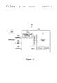
- FIG. 3is a block diagram of a system in which some embodiments of present invention can be practiced.
- FIG. 1shows an exploded perspective view of some embodiments of chip carrier system 100 which comprises two basic components, module 103 and socket 106 .
- FIG. 1also shows printed circuit board 109 on which chip carrier system 100 can be mounted.
- chip carrier system 100is capable of packaging and interconnecting a variety of integrated circuits, such as analog circuits, mixed signal application specific circuits, and digital circuits, it is particularly suited through its modular embodiment to applications involving the packaging of memory circuits.
- Module 103in one embodiment, comprises substrate 112 , edges 114 , 115 , 116 , and 117 , chip 118 , and alignment feature 124 .
- Chip 118is mounted on substrate 112 .
- Substrate 112in one embodiment, is made of a conducting material, such as copper, aluminum or gold, or an alloy of such a conducting material.
- One function of substrate 112is to transfer heat away from chip 118 . Fabricating substrate 112 from a material that is not a good conductor can lead to the catastrophic failure of chip 118 , if the material selected for substrate 112 fails to efficiently transfer heat away from chip 118 .
- Chip 118in one embodiment, is mounted face down on substrate 112 , and is secured to substrate 112 using a heat conducting adhesive.
- the heat conducting adhesiveprovides a path for the heat generated by chip 118 to flow into substrate 112 .
- the rate at which heat is removed from chip 118can be increased by directing air flow across the surface of substrate 112 .
- Chip 118includes coupling site 127 , which in one embodiment comprises contact pads 130 .
- Contact pads 130provide a direct connection to the circuits and devices on chip 118 .
- coupling site 127comprises pins or other similar connectors, and these pins or other similar connectors are in turn coupled to contact pads 130 .
- Edges 114 , 115 , 116 and 117are preferably planar surfaces.
- a planar surfacemakes substrate 112 simple to manufacture, easy to grasp, and permits quick insertion of module 103 into socket 106 .
- Alignment feature 124is used to register module 103 with socket 106 .
- module coupling site 127is aligned with socket coupling site 133 .
- Alignment of module coupling site 127 with socket coupling site 133permits communication between chip 118 and the circuits, chips or devices located on circuit board 109 or coupled to circuit board 109 . Failure to align module coupling site 127 to socket coupling site 133 may result in the isolation of chip 118 from the circuits, chips or devices located on circuit board 109 .
- Alignment feature 124in one embodiment, is a curved indentation or notch capable of interlocking with a half-cylinder, which is the corresponding alignment feature located on socket 106 .
- This configuration of alignment featurespermits the insertion of module 103 into socket 106 using a low or zero insertion force, yet restricts the motion of module 103 with respect to socket 106 in the non-lateral direction. Restricting the motion of module 103 in the non-lateral direction ensures the continued alignment of coupling site 127 with socket coupling site 133 .
- Socket 106in one embodiment, comprises edge 134 , surface 136 , alignment feature 139 , guide 142 , socket coupling site 133 , and retaining feature 147 .
- Socket 106is preferably an injection molded component made of nylon or any other suitable plastic material. Alternatively, socket 106 can be machined from a single piece of plastic or other appropriate material.
- Guide 142is located along edge 134 of socket 106 .
- Guide 142in one embodiment, has the shape of an el, as shown in FIG. 1, and can be fabricated as an integrated component of socket 106 .
- El shaped guide 142provides for quick, easy and accurate insertion of module 103 into guide 142 . Once inserted into guide 142 , module 103 slides along the inside edge of guide 142 until it is seated in socket 106 .
- An advantage of this embodimentis that an untrained person can successfully insert module 103 into socket 106 without damaging components of either module 103 or socket 106 .
- Alignment feature 139interlocks with module alignment feature 124 .
- alignment feature 139has a smooth shape, such as the shape of a half cylinder as shown in FIG. 1 .
- a half cylinder shapewhich lacks sharp corners, for alignment feature 139 makes the final alignment and interlocking of module 103 with socket 106 an easy operation to perform.
- Module 103slides easily into place once module alignment feature 124 engages socket alignment feature 139 , since there are no sharp corners to interfere with the interlocking of module alignment feature 124 with socket alignment feature 139 .
- the present inventionis not limited to alignment feature 139 having a half cylinder shape. Other shapes will also permit easy insertion of module 103 into socket 106 .
- Socket alignment feature 139is approximately centered along the longest dimension of surface 136 of socket 106 , and is preferably fabricated as an integrated component of socket 106 . Centering socket alignment feature 139 makes the operation of inserting module 103 into socket 106 and interlocking module 103 with module 106 easier than if the socket alignment feature 139 is located off center. Socket alignment feature 139 also serves to restrict the non-lateral motion of module 103 , which keeps module coupling site 127 aligned with socket coupling site 133 .
- Retaining feature 147restricts the lateral motion of module 103 .
- retaining feature 147is a lip located along an edge of surface 136 . Restricting the lateral motion of module 103 forces module coupling site 127 to stay coupled to socket coupling site 133 .
- the location of retaining feature 147 and the amount to which the lateral motion of module 103 is restrictedis determined by the characteristics of module coupling site 127 and socket coupling site 133 . If module coupling site 127 comprises pads on an integrated circuit chip, and coupling site 133 comprises contacts for those pads, then the proper amount of restriction is achieved by having retaining feature 147 located such that module 103 couples to socket 106 with an amount of force equivalent to a press fit.
- retaining feature 139is preferably fabricated as an integrated component of socket 106 .
- Printed circuit board 109provides a platform for mounting socket 106 , and a platform on which other circuit modules, such as circuit module 150 , can be mounted and coupled to socket 106 .
- the present inventionis not limited to a particular type of printed circuit board technology.
- Socket 106can be mounted on a single or multilayer board, and can be secured to the board using an adhesive. Alternatively, socket 106 can be secured to the board using an epoxy.
- FIG. 2is a side view of some embodiments of an assembled chip carrier system 100 of the present invention.
- Module 103is assembled with socket 106 using a press fit, and the assembled chip carrier system 100 is mounted on printed circuit board 109 .
- module 103is interlocked with socket 106 at module alignment feature 124 and socket alignment feature 139 .
- socket alignment feature 139The seating and retention of module 103 in socket 106 is best understood by describing the functioning of socket alignment feature 139 , module alignment feature 124 , retaining feature 147 , and guide 142 in the assembled chip carrier system 100 .
- Socket alignment feature 139 and module alignment feature 124restrict the non-lateral motion of module 103 once socket alignment feature 139 is interlocked with module alignment feature 124 .
- Retaining feature 147abuts module 103 , and ensures that socket coupling site 133 is in contact with module coupling site 127 by restricting the lateral motion of module 103 after module 103 is seated in socket 106 .
- Guide 142assists retaining feature 147 in keeping module coupling site 127 in contact with socket coupling site 133 by restricting the lateral motion of the top of module 103 .
- Signalscan flow from chip 118 mounted on substrate 103 to circuit module 150 mounted on printed circuit board 109 .
- the flow of signals between chip 118 and module 150is best understood by following the conducting pattern from socket coupling site 133 to circuit module 150 .
- Module coupling site 127is in contact with socket coupling site 133 .
- Conductor 152couples socket coupling site 133 to socket board contact site 155 .
- a second conductor 158couples circuit board contact site 155 to circuit module 150 .
- System 300comprises processor 305 and memory device 310 , which includes memory cells of one or more of the types described above in conjunction with FIGS. 1-2.
- Memory device 310comprises memory array 315 , address circuitry 320 , and read circuitry 330 , and is coupled to processor 305 by address bus 335 , data bus 340 , and control bus 345 .
- Processor 305through address bus 335 , data bus 340 , and control bus 345 communicates with memory device 310 .
- address information, data information, and control informationare provided to memory device 310 through busses 335 , 340 , and 345 .
- This informationis decoded by addressing circuitry 320 , including a row decoder and a column decoder, and read circuitry 330 . Successful completion of the read operation results in information from memory array 315 being communicated to processor 305 over data bus 340 .
- Memory circuits or cellswhen mounted in the chip carrier system of the present invention, become addressable as elements of memory array 315 in the system shown in FIG. 3 .
- Embodiments of an apparatus and method for packaging circuitshas been described.
- a module and socket capable of being easily aligned, assembled and interlockedhas been described.
- a substrate, a chip, and a socketalso capable of being easily aligned, assembled and interlocked has been described.
- a method of aligning a module with the guide feature of a socket, sliding the module along the edge of the guide, and interlocking the module with the sockethas been described.
Landscapes
- Coupling Device And Connection With Printed Circuit (AREA)
- Combinations Of Printed Boards (AREA)
Abstract
Description
Claims (83)
Priority Applications (2)
| Application Number | Priority Date | Filing Date | Title |
|---|---|---|---|
| US09/261,608US6419517B1 (en) | 1999-02-26 | 1999-02-26 | Apparatus and method for packaging circuits |
| US10/196,103US6537100B2 (en) | 1999-02-26 | 2002-07-15 | Apparatus and method for packaging circuits |
Applications Claiming Priority (1)
| Application Number | Priority Date | Filing Date | Title |
|---|---|---|---|
| US09/261,608US6419517B1 (en) | 1999-02-26 | 1999-02-26 | Apparatus and method for packaging circuits |
Related Child Applications (1)
| Application Number | Title | Priority Date | Filing Date |
|---|---|---|---|
| US10/196,103ContinuationUS6537100B2 (en) | 1999-02-26 | 2002-07-15 | Apparatus and method for packaging circuits |
Publications (2)
| Publication Number | Publication Date |
|---|---|
| US20020037665A1 US20020037665A1 (en) | 2002-03-28 |
| US6419517B1true US6419517B1 (en) | 2002-07-16 |
Family
ID=22994072
Family Applications (2)
| Application Number | Title | Priority Date | Filing Date |
|---|---|---|---|
| US09/261,608Expired - LifetimeUS6419517B1 (en) | 1999-02-26 | 1999-02-26 | Apparatus and method for packaging circuits |
| US10/196,103Expired - LifetimeUS6537100B2 (en) | 1999-02-26 | 2002-07-15 | Apparatus and method for packaging circuits |
Family Applications After (1)
| Application Number | Title | Priority Date | Filing Date |
|---|---|---|---|
| US10/196,103Expired - LifetimeUS6537100B2 (en) | 1999-02-26 | 2002-07-15 | Apparatus and method for packaging circuits |
Country Status (1)
| Country | Link |
|---|---|
| US (2) | US6419517B1 (en) |
Cited By (3)
| Publication number | Priority date | Publication date | Assignee | Title |
|---|---|---|---|---|
| US6816390B1 (en)* | 2003-11-05 | 2004-11-09 | International Business Machines Corporation | Apparatus for blind swap cassette guidance |
| US20120295469A1 (en)* | 2011-04-26 | 2012-11-22 | Honda Elesys Co., Ltd. | Electronic device having connector |
| US20140313646A1 (en)* | 2013-04-22 | 2014-10-23 | Hon Hai Precision Industry Co., Ltd. | Attachment mechanism for fastening expansion card |
Families Citing this family (1)
| Publication number | Priority date | Publication date | Assignee | Title |
|---|---|---|---|---|
| CN100552932C (en)* | 2007-11-13 | 2009-10-21 | 日月光半导体制造股份有限公司 | Packaging structure capable of connecting output/input module |
Citations (23)
| Publication number | Priority date | Publication date | Assignee | Title |
|---|---|---|---|---|
| US3364458A (en)* | 1966-06-01 | 1968-01-16 | Kernforschungsanlage Juelich | Unviersal extension connector for use with indexed printed circuit boards and connector plugs |
| US4781612A (en) | 1983-12-14 | 1988-11-01 | Amp Incorporated | Socket for single in-line memory module |
| US4892487A (en)* | 1989-06-15 | 1990-01-09 | Ibm Corporation | Connector assembly with movable carriage |
| US4995825A (en) | 1990-03-19 | 1991-02-26 | Amp Incorporated | Electronic module socket with resilient latch |
| US5040997A (en)* | 1990-06-08 | 1991-08-20 | The Foxboro Company | Flex circuit connector assembly and method for manufacturing the same |
| US5209675A (en) | 1991-07-02 | 1993-05-11 | The Whitaker Corporation | Electronic module socket with resilient latch |
| US5244403A (en) | 1991-04-10 | 1993-09-14 | Augat Inc. | Electronic component socket with external latch |
| US5256078A (en) | 1991-10-04 | 1993-10-26 | E. I. Du Pont De Nemours And Company | Electrical socket |
| US5266833A (en) | 1992-03-30 | 1993-11-30 | Capps David F | Integrated circuit bus structure |
| US5360992A (en) | 1991-12-20 | 1994-11-01 | Micron Technology, Inc. | Two piece assembly for the selection of pinouts and bond options on a semiconductor device |
| USRE34794E (en) | 1989-11-06 | 1994-11-22 | Micron Technology, Inc. | Gull-wing zig-zag inline lead package having end-of-package anchoring pins |
| US5403202A (en)* | 1993-10-07 | 1995-04-04 | Hewlett-Packard Company | Low insertion force/low profile flex connector |
| US5444304A (en) | 1992-08-24 | 1995-08-22 | Hitachi, Ltd. | Semiconductor device having a radiating part |
| US5450289A (en) | 1993-03-05 | 1995-09-12 | Samsung Electronics Co., Ltd. | Semiconductor package and a printed circuit board applicable to its mounting |
| US5451815A (en) | 1993-06-25 | 1995-09-19 | Fujitsu Limited | Semiconductor device with surface mount package adapted for vertical mounting |
| US5592019A (en) | 1994-04-19 | 1997-01-07 | Mitsubishi Denki Kabushiki Kaisha | Semiconductor device and module |
| US5593927A (en) | 1993-10-14 | 1997-01-14 | Micron Technology, Inc. | Method for packaging semiconductor dice |
| US5635760A (en) | 1993-07-01 | 1997-06-03 | Nec Corporation | Surface mount semiconductor device |
| US5642261A (en)* | 1993-12-20 | 1997-06-24 | Sgs-Thomson Microelectronics, Inc. | Ball-grid-array integrated circuit package with solder-connected thermal conductor |
| US5668409A (en) | 1995-06-05 | 1997-09-16 | Harris Corporation | Integrated circuit with edge connections and method |
| US5872701A (en)* | 1997-02-27 | 1999-02-16 | Tandem Computers, Incorporated | Blind alignment method and apparatus for circuit boards |
| US6030251A (en)* | 1998-02-17 | 2000-02-29 | Intel Corporation | Keyed interlock and mechanical alignment integrated mechanical retention features for PC system |
| US6115254A (en)* | 1998-04-15 | 2000-09-05 | Micron Technology, Inc. | Vertical surface mount apparatus with thermal carrier |
Family Cites Families (6)
| Publication number | Priority date | Publication date | Assignee | Title |
|---|---|---|---|---|
| US4744764A (en)* | 1986-05-27 | 1988-05-17 | Rogers Corporation | Connector arrangement |
| US5186632A (en)* | 1991-09-20 | 1993-02-16 | International Business Machines Corporation | Electronic device elastomeric mounting and interconnection technology |
| US5335146A (en)* | 1992-01-29 | 1994-08-02 | International Business Machines Corporation | High density packaging for device requiring large numbers of unique signals utilizing orthogonal plugging and zero insertion force connetors |
| US5748426A (en)* | 1996-04-29 | 1998-05-05 | Paradyne Corporation | Method for interfacing to a powered bus |
| US6191474B1 (en)* | 1997-12-31 | 2001-02-20 | Micron Technology, Inc. | Vertically mountable interposer assembly and method |
| US6087723A (en)* | 1998-03-30 | 2000-07-11 | Micron Technology, Inc. | Vertical surface mount assembly and methods |
- 1999
- 1999-02-26USUS09/261,608patent/US6419517B1/ennot_activeExpired - Lifetime
- 2002
- 2002-07-15USUS10/196,103patent/US6537100B2/ennot_activeExpired - Lifetime
Patent Citations (24)
| Publication number | Priority date | Publication date | Assignee | Title |
|---|---|---|---|---|
| US3364458A (en)* | 1966-06-01 | 1968-01-16 | Kernforschungsanlage Juelich | Unviersal extension connector for use with indexed printed circuit boards and connector plugs |
| US4781612A (en) | 1983-12-14 | 1988-11-01 | Amp Incorporated | Socket for single in-line memory module |
| US4892487A (en)* | 1989-06-15 | 1990-01-09 | Ibm Corporation | Connector assembly with movable carriage |
| USRE34794E (en) | 1989-11-06 | 1994-11-22 | Micron Technology, Inc. | Gull-wing zig-zag inline lead package having end-of-package anchoring pins |
| US4995825A (en) | 1990-03-19 | 1991-02-26 | Amp Incorporated | Electronic module socket with resilient latch |
| US5040997A (en)* | 1990-06-08 | 1991-08-20 | The Foxboro Company | Flex circuit connector assembly and method for manufacturing the same |
| US5244403A (en) | 1991-04-10 | 1993-09-14 | Augat Inc. | Electronic component socket with external latch |
| US5209675A (en) | 1991-07-02 | 1993-05-11 | The Whitaker Corporation | Electronic module socket with resilient latch |
| US5256078A (en) | 1991-10-04 | 1993-10-26 | E. I. Du Pont De Nemours And Company | Electrical socket |
| US5360992A (en) | 1991-12-20 | 1994-11-01 | Micron Technology, Inc. | Two piece assembly for the selection of pinouts and bond options on a semiconductor device |
| US5266833A (en) | 1992-03-30 | 1993-11-30 | Capps David F | Integrated circuit bus structure |
| US5444304A (en) | 1992-08-24 | 1995-08-22 | Hitachi, Ltd. | Semiconductor device having a radiating part |
| US5450289A (en) | 1993-03-05 | 1995-09-12 | Samsung Electronics Co., Ltd. | Semiconductor package and a printed circuit board applicable to its mounting |
| US5451815A (en) | 1993-06-25 | 1995-09-19 | Fujitsu Limited | Semiconductor device with surface mount package adapted for vertical mounting |
| US5635760A (en) | 1993-07-01 | 1997-06-03 | Nec Corporation | Surface mount semiconductor device |
| US5403202A (en)* | 1993-10-07 | 1995-04-04 | Hewlett-Packard Company | Low insertion force/low profile flex connector |
| US5593927A (en) | 1993-10-14 | 1997-01-14 | Micron Technology, Inc. | Method for packaging semiconductor dice |
| US5642261A (en)* | 1993-12-20 | 1997-06-24 | Sgs-Thomson Microelectronics, Inc. | Ball-grid-array integrated circuit package with solder-connected thermal conductor |
| US5592019A (en) | 1994-04-19 | 1997-01-07 | Mitsubishi Denki Kabushiki Kaisha | Semiconductor device and module |
| US5668409A (en) | 1995-06-05 | 1997-09-16 | Harris Corporation | Integrated circuit with edge connections and method |
| US5872701A (en)* | 1997-02-27 | 1999-02-16 | Tandem Computers, Incorporated | Blind alignment method and apparatus for circuit boards |
| US6030251A (en)* | 1998-02-17 | 2000-02-29 | Intel Corporation | Keyed interlock and mechanical alignment integrated mechanical retention features for PC system |
| US6115254A (en)* | 1998-04-15 | 2000-09-05 | Micron Technology, Inc. | Vertical surface mount apparatus with thermal carrier |
| US6134111A (en)* | 1998-04-15 | 2000-10-17 | Micron Technology, Inc. | Vertical surface mount apparatus with thermal carrier |
Cited By (5)
| Publication number | Priority date | Publication date | Assignee | Title |
|---|---|---|---|---|
| US6816390B1 (en)* | 2003-11-05 | 2004-11-09 | International Business Machines Corporation | Apparatus for blind swap cassette guidance |
| US20120295469A1 (en)* | 2011-04-26 | 2012-11-22 | Honda Elesys Co., Ltd. | Electronic device having connector |
| US8545238B2 (en)* | 2011-04-26 | 2013-10-01 | Honda Elesys Co., Ltd. | Electronic device having connector |
| US20140313646A1 (en)* | 2013-04-22 | 2014-10-23 | Hon Hai Precision Industry Co., Ltd. | Attachment mechanism for fastening expansion card |
| US9152188B2 (en)* | 2013-04-22 | 2015-10-06 | Hon Hai Precision Industry Co., Ltd. | Attachment mechanism for fastening expansion card |
Also Published As
| Publication number | Publication date |
|---|---|
| US20020037665A1 (en) | 2002-03-28 |
| US20020182926A1 (en) | 2002-12-05 |
| US6537100B2 (en) | 2003-03-25 |
Similar Documents
| Publication | Publication Date | Title |
|---|---|---|
| US6721189B1 (en) | Memory module | |
| US4766371A (en) | Test board for semiconductor packages | |
| US7639027B2 (en) | Method of testing circuit elements on a semiconductor wafer | |
| US5186632A (en) | Electronic device elastomeric mounting and interconnection technology | |
| US6435882B1 (en) | Socketable flexible circuit based electronic device module and a socket for the same | |
| US6200144B1 (en) | Interposer/converter to allow single-sided contact to circuit modules | |
| US7129730B2 (en) | Probe card assembly | |
| US20020025726A1 (en) | Card connector | |
| US6704204B1 (en) | IC package with edge connect contacts | |
| US6454572B1 (en) | Surface mount connector | |
| JP2001313107A (en) | Card connector | |
| US20100032820A1 (en) | Stacked Memory Module | |
| WO1997014195A1 (en) | Low-profile zero-insertion-force socket | |
| EP1538710B1 (en) | Memory card connector | |
| US6419517B1 (en) | Apparatus and method for packaging circuits | |
| JPH0855659A (en) | Manufacturing process of receptacle connector for ic card | |
| US6109930A (en) | Enhanced hardware arrangement for mounting a plurality of circuit boards together | |
| US6234829B1 (en) | Method and device for identifying card slots that are required to be populated concurrently in a computer system | |
| US6774483B2 (en) | Semiconductor assembly with a semiconductor module | |
| JPH08512168A (en) | High-density electronic device connector | |
| US6729896B2 (en) | Electrical connector with distortion-resistant cover | |
| JP3316095B2 (en) | Integrated circuit die test system | |
| US7094068B2 (en) | Load board | |
| EP0905521A2 (en) | Burn-in testing device | |
| US6549420B2 (en) | Method and apparatus for increasing memory capacity |
Legal Events
| Date | Code | Title | Description |
|---|---|---|---|
| AS | Assignment | Owner name:MICRON TECHNOLOGY, INC., IDAHO Free format text:ASSIGNMENT OF ASSIGNORS INTEREST;ASSIGNOR:MODEN, WALTER L.;REEL/FRAME:009986/0543 Effective date:19990423 | |
| STCF | Information on status: patent grant | Free format text:PATENTED CASE | |
| CC | Certificate of correction | ||
| FPAY | Fee payment | Year of fee payment:4 | |
| FPAY | Fee payment | Year of fee payment:8 | |
| FPAY | Fee payment | Year of fee payment:12 | |
| AS | Assignment | Owner name:U.S. BANK NATIONAL ASSOCIATION, AS COLLATERAL AGENT, CALIFORNIA Free format text:SECURITY INTEREST;ASSIGNOR:MICRON TECHNOLOGY, INC.;REEL/FRAME:038669/0001 Effective date:20160426 Owner name:U.S. BANK NATIONAL ASSOCIATION, AS COLLATERAL AGEN Free format text:SECURITY INTEREST;ASSIGNOR:MICRON TECHNOLOGY, INC.;REEL/FRAME:038669/0001 Effective date:20160426 | |
| AS | Assignment | Owner name:MORGAN STANLEY SENIOR FUNDING, INC., AS COLLATERAL AGENT, MARYLAND Free format text:PATENT SECURITY AGREEMENT;ASSIGNOR:MICRON TECHNOLOGY, INC.;REEL/FRAME:038954/0001 Effective date:20160426 Owner name:MORGAN STANLEY SENIOR FUNDING, INC., AS COLLATERAL Free format text:PATENT SECURITY AGREEMENT;ASSIGNOR:MICRON TECHNOLOGY, INC.;REEL/FRAME:038954/0001 Effective date:20160426 | |
| AS | Assignment | Owner name:U.S. BANK NATIONAL ASSOCIATION, AS COLLATERAL AGENT, CALIFORNIA Free format text:CORRECTIVE ASSIGNMENT TO CORRECT THE REPLACE ERRONEOUSLY FILED PATENT #7358718 WITH THE CORRECT PATENT #7358178 PREVIOUSLY RECORDED ON REEL 038669 FRAME 0001. ASSIGNOR(S) HEREBY CONFIRMS THE SECURITY INTEREST;ASSIGNOR:MICRON TECHNOLOGY, INC.;REEL/FRAME:043079/0001 Effective date:20160426 Owner name:U.S. BANK NATIONAL ASSOCIATION, AS COLLATERAL AGEN Free format text:CORRECTIVE ASSIGNMENT TO CORRECT THE REPLACE ERRONEOUSLY FILED PATENT #7358718 WITH THE CORRECT PATENT #7358178 PREVIOUSLY RECORDED ON REEL 038669 FRAME 0001. ASSIGNOR(S) HEREBY CONFIRMS THE SECURITY INTEREST;ASSIGNOR:MICRON TECHNOLOGY, INC.;REEL/FRAME:043079/0001 Effective date:20160426 | |
| AS | Assignment | Owner name:JPMORGAN CHASE BANK, N.A., AS COLLATERAL AGENT, ILLINOIS Free format text:SECURITY INTEREST;ASSIGNORS:MICRON TECHNOLOGY, INC.;MICRON SEMICONDUCTOR PRODUCTS, INC.;REEL/FRAME:047540/0001 Effective date:20180703 Owner name:JPMORGAN CHASE BANK, N.A., AS COLLATERAL AGENT, IL Free format text:SECURITY INTEREST;ASSIGNORS:MICRON TECHNOLOGY, INC.;MICRON SEMICONDUCTOR PRODUCTS, INC.;REEL/FRAME:047540/0001 Effective date:20180703 | |
| AS | Assignment | Owner name:MICRON TECHNOLOGY, INC., IDAHO Free format text:RELEASE BY SECURED PARTY;ASSIGNOR:U.S. BANK NATIONAL ASSOCIATION, AS COLLATERAL AGENT;REEL/FRAME:047243/0001 Effective date:20180629 | |
| AS | Assignment | Owner name:MICRON TECHNOLOGY, INC., IDAHO Free format text:RELEASE BY SECURED PARTY;ASSIGNOR:MORGAN STANLEY SENIOR FUNDING, INC., AS COLLATERAL AGENT;REEL/FRAME:050937/0001 Effective date:20190731 | |
| AS | Assignment | Owner name:MICRON TECHNOLOGY, INC., IDAHO Free format text:RELEASE BY SECURED PARTY;ASSIGNOR:JPMORGAN CHASE BANK, N.A., AS COLLATERAL AGENT;REEL/FRAME:051028/0001 Effective date:20190731 Owner name:MICRON SEMICONDUCTOR PRODUCTS, INC., IDAHO Free format text:RELEASE BY SECURED PARTY;ASSIGNOR:JPMORGAN CHASE BANK, N.A., AS COLLATERAL AGENT;REEL/FRAME:051028/0001 Effective date:20190731 |