US6418537B1 - Accurate timing calibration for each of multiple high-speed clocked receivers using a single DLL - Google Patents
Accurate timing calibration for each of multiple high-speed clocked receivers using a single DLLDownload PDFInfo
- Publication number
- US6418537B1 US6418537B1US09/350,414US35041499AUS6418537B1US 6418537 B1US6418537 B1US 6418537B1US 35041499 AUS35041499 AUS 35041499AUS 6418537 B1US6418537 B1US 6418537B1
- Authority
- US
- United States
- Prior art keywords
- phases
- data
- local
- bit
- clock
- Prior art date
- Legal status (The legal status is an assumption and is not a legal conclusion. Google has not performed a legal analysis and makes no representation as to the accuracy of the status listed.)
- Expired - Lifetime
Links
Images


Classifications
- G—PHYSICS
- G06—COMPUTING OR CALCULATING; COUNTING
- G06F—ELECTRIC DIGITAL DATA PROCESSING
- G06F12/00—Accessing, addressing or allocating within memory systems or architectures
- G06F12/02—Addressing or allocation; Relocation
- G06F12/08—Addressing or allocation; Relocation in hierarchically structured memory systems, e.g. virtual memory systems
- G06F12/0802—Addressing of a memory level in which the access to the desired data or data block requires associative addressing means, e.g. caches
- G06F12/0806—Multiuser, multiprocessor or multiprocessing cache systems
- G06F12/0813—Multiuser, multiprocessor or multiprocessing cache systems with a network or matrix configuration
- G—PHYSICS
- G06—COMPUTING OR CALCULATING; COUNTING
- G06F—ELECTRIC DIGITAL DATA PROCESSING
- G06F1/00—Details not covered by groups G06F3/00 - G06F13/00 and G06F21/00
- G06F1/04—Generating or distributing clock signals or signals derived directly therefrom
- G—PHYSICS
- G06—COMPUTING OR CALCULATING; COUNTING
- G06F—ELECTRIC DIGITAL DATA PROCESSING
- G06F12/00—Accessing, addressing or allocating within memory systems or architectures
- G06F12/02—Addressing or allocation; Relocation
- G06F12/08—Addressing or allocation; Relocation in hierarchically structured memory systems, e.g. virtual memory systems
- G06F12/0802—Addressing of a memory level in which the access to the desired data or data block requires associative addressing means, e.g. caches
- G06F12/0806—Multiuser, multiprocessor or multiprocessing cache systems
- G06F12/0815—Cache consistency protocols
- G06F12/0817—Cache consistency protocols using directory methods
- G06F12/0822—Copy directories
- G—PHYSICS
- G06—COMPUTING OR CALCULATING; COUNTING
- G06F—ELECTRIC DIGITAL DATA PROCESSING
- G06F15/00—Digital computers in general; Data processing equipment in general
- G06F15/16—Combinations of two or more digital computers each having at least an arithmetic unit, a program unit and a register, e.g. for a simultaneous processing of several programs
- G06F15/163—Interprocessor communication
- G06F15/173—Interprocessor communication using an interconnection network, e.g. matrix, shuffle, pyramid, star, snowflake
- G06F15/17356—Indirect interconnection networks
- G06F15/17368—Indirect interconnection networks non hierarchical topologies
- G06F15/17375—One dimensional, e.g. linear array, ring
- G—PHYSICS
- G06—COMPUTING OR CALCULATING; COUNTING
- G06F—ELECTRIC DIGITAL DATA PROCESSING
- G06F3/00—Input arrangements for transferring data to be processed into a form capable of being handled by the computer; Output arrangements for transferring data from processing unit to output unit, e.g. interface arrangements
- H—ELECTRICITY
- H03—ELECTRONIC CIRCUITRY
- H03L—AUTOMATIC CONTROL, STARTING, SYNCHRONISATION OR STABILISATION OF GENERATORS OF ELECTRONIC OSCILLATIONS OR PULSES
- H03L7/00—Automatic control of frequency or phase; Synchronisation
- H—ELECTRICITY
- H04—ELECTRIC COMMUNICATION TECHNIQUE
- H04L—TRANSMISSION OF DIGITAL INFORMATION, e.g. TELEGRAPHIC COMMUNICATION
- H04L25/00—Baseband systems
- H04L25/02—Details ; arrangements for supplying electrical power along data transmission lines
- H04L25/0264—Arrangements for coupling to transmission lines
- H04L25/0272—Arrangements for coupling to multiple lines, e.g. for differential transmission
- H—ELECTRICITY
- H04—ELECTRIC COMMUNICATION TECHNIQUE
- H04L—TRANSMISSION OF DIGITAL INFORMATION, e.g. TELEGRAPHIC COMMUNICATION
- H04L7/00—Arrangements for synchronising receiver with transmitter
- H04L7/02—Speed or phase control by the received code signals, the signals containing no special synchronisation information
- H04L7/033—Speed or phase control by the received code signals, the signals containing no special synchronisation information using the transitions of the received signal to control the phase of the synchronising-signal-generating means, e.g. using a phase-locked loop
- H04L7/0337—Selecting between two or more discretely delayed clocks or selecting between two or more discretely delayed received code signals
- H—ELECTRICITY
- H04—ELECTRIC COMMUNICATION TECHNIQUE
- H04L—TRANSMISSION OF DIGITAL INFORMATION, e.g. TELEGRAPHIC COMMUNICATION
- H04L7/00—Arrangements for synchronising receiver with transmitter
- H04L7/0008—Synchronisation information channels, e.g. clock distribution lines
- H04L7/0012—Synchronisation information channels, e.g. clock distribution lines by comparing receiver clock with transmitter clock
- H—ELECTRICITY
- H04—ELECTRIC COMMUNICATION TECHNIQUE
- H04L—TRANSMISSION OF DIGITAL INFORMATION, e.g. TELEGRAPHIC COMMUNICATION
- H04L7/00—Arrangements for synchronising receiver with transmitter
- H04L7/04—Speed or phase control by synchronisation signals
- H04L7/041—Speed or phase control by synchronisation signals using special codes as synchronising signal
- H—ELECTRICITY
- H04—ELECTRIC COMMUNICATION TECHNIQUE
- H04L—TRANSMISSION OF DIGITAL INFORMATION, e.g. TELEGRAPHIC COMMUNICATION
- H04L7/00—Arrangements for synchronising receiver with transmitter
- H04L7/04—Speed or phase control by synchronisation signals
- H04L7/10—Arrangements for initial synchronisation
Definitions
- the present inventionoptimizes clock timing for each received channel bit while only using a single DLL for all received bits. It thus provides the benefits of a dedicated DLL per received channel bit, without the associated cost.
- each group of transmitter bitsalso employs an additional associated PLL.
- the present inventionpermits data rates as high as 1.6 Gbit/s on each pair of differential wires of a multiple-bit parallel channel. This rate is achieved even with data skew between data bits as large as 2-bit-times.
- the inventionuses an 8-to-1 data serialization circuit in the transmitter to convert 80-bit parallel 200 MHz data to 10-bit parallel 1.6 Mb/s data.
- the datais signaled over a multiple-bit parallel channel that uses 10-bits transmit, 10-bits receive, and a forwarded clock in each of two directions.
- the serialized dataare captured using a forwarded clock and de-serialized.
- a DLLgenerates 16 master phases without reference to the word boundaries of data being transmitted. These 16 unreferenced phases are input to a phase rotator that, via a series of calibration steps, maps the unreferenced phases into named phases, and in doing so references the phases to the word boundary of the data being transmitted over the slowest data line of the parallel channel.
- the named phasesare then input to a data interpolator in each receiver, which generates 16 local phases.
- the 16 local phasescorrespond to the data-bit centers and data-bit edges for each of the 8 bits transferred per miajor channel clock period.
- a bit-centering calibration stepa training pattern is evaluated by each receiver and each data interpolator dynamically adjusts a delay applied to the 16 local phases to establish the local center-data phases in the center of the bits received by the corresponding receiver.
- 8 contiguous bitsare selected as the data outputs from a 10-bit window.
- the local center-data phasesare used to serialize and de-serialize the channel data for the receiver.
- the present inventionfinds particular application in the design of the channel interface circuitry for contemporary high-speed multiprocessor systems, such as those disclosed in the applications previously incorporated by reference above.
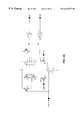
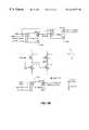
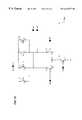
- FIG. 1 ais an abstract drawing showing one system environment in which the invention functions.
- FIG. 1 bis a block diagram of the major components of the invention.
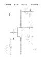
- FIG. 1 cis a block diagram of the calibration control logic 700 of FIG. 1 a.
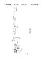
- FIG. 2illustrates how the receiver and transmitter logic of FIGS. 1 a and 1 b is extended for use in multiple bit parallel data channels.
- FIGS. 3 a - dshow the circuitry and function blocks that make up the per-bit receive logic of block 500 of FIG. 1 b.
- FIG. 4is a circuit diagram of the phase detector 350 of FIG. 1 b and FIG. 3 c.
- FIG. 5shows the circuitry and function blocks that make up the delay interpolator block 250 of FIG. 1 b and FIG. 3 d.
- FIG. 6is the circuit diagram of the bias block 2510 of the delay interpolitor of FIG. 5 .
- FIG. 7is the circuit diagram of the delay stages 2520 of the delay interpolator of FIG. 5 .
- FIG. 8is the circuit diagram of the diff 2 cmos block 2530 of the delay interpolator of FIG. 5 .
- FIGS. 9 a - bis the circuitry and function blocks of the phase rotator 75 of FIG. 1 b.
- FIG. 10is the circuit diagram of the 8-to-1 multiplexer blocks 7510 of the phase rotator of FIG. 9 a.
- FIG. 11is the circuit diagram of the d 11 _delay_x 2 block 7520 of the phase rotator of FIG. 9 b.
- FIG. 12is the circuit diagram of the d 11 _delay_x 4 block 7540 of the phase rotator of FIG. 9 b.
- FIG. 13is the circuit diagram of the d 11 _delay_x 6 block 7560 of the phase rotator of FIG. 9 b.
- FIG. 14shows timing diagrams showing the possible bit-centering calibration cases.
- FIG. 15is a diagram of the window selection logic 600 of FIG. 1 b.
- FIG. 1 ais an abstract drawing showing the system environment of an illustrative embodiment.
- the inventionis incorporated into the channel transceiver logic of each of two chips in communication with each other over a point-to-point communications channel.
- FIG. 2illustrates how the receiver and transmitter logic of FIGS. 1 a and 1 b is extended for use in multiple-bit parallel data channels in a preferred embodiment.
- the datais signaled over a multiple-bit parallel channel that uses 10-bits transmit, 10-bits receive, and a forwarded clock in each of two directions.
- An 8-to-1 data serialization circuit in the transmitterto convert 80-bit parallel 200 MHz data to 10-bit parallel 1.6 Mb/s data.
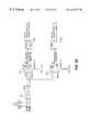
- FIG. 1 bis a block diagram of the major components of the invention.
- Block 100includes ESD Network 25 , a Multi-tap DLL, and a phase rotator (also referred to as a clock switch) 75 . As illustrated in FIG. 2, only one block 100 is implemented for a plurality of channel bit lines.
- FIGS. 3A-Dshow the circuitry and function blocks that make up the per-bit receive logic of block 500 of FIG. 1 b . Block 500 is replicated for each channel data-bit.
- the receiverconverts the incoming 200 MHz clock 15 into 16 phases (8 center data phases and 8 edge data phases) 55 with a Delay Locked Loop (DLL) 50 having multiple taps (one tap per phase output) . The beginning of each phase is separated by 312 ps. These clocks (phases) are then fed into a clock phase rotator 75 controlled by 3-bit digital control signals 60 . The 16 clock phases out 80 of the clock phase rotator are distributed to each per-wire data receiver 1000 . Each data receiver has its own delay interpolator 250 , which is controlled by 4 bit digital signals 225 , and capable of delaying the clock Lip to one dlata bit (625 ps). Each data receiver has 16 differential data capture latches 300 that are timed by the 16 clock phases 275 generated from its local delay interpolator. The purpose of this delay interpolation is to optimize the clock position relative to data bits.
- DLLDelay Locked Loop
- a preferred training pattern of 10100111is used. This patter has enough transition edges to permit bit-timing adjustment. Under control of calibration control logic 700 , the pattern is 2 ⁇ over-sampled every 64 core clock cycles and compared in a charge pump circuit 350 to provide an up/down signal 355 to indicate the required direction of local clock edge movement. The bit timing adjustments will converge within a few microseconds.
- the charge pumpeffectively performs statistical averaging of the bit-centering status over all the bit lines. More specifically, the charge pump implements an exclusive-or compare of the pattern data sampled by the center and edge clock phases for each bit line. The pump ties the output circuitry of each exclusive-or to a single capacitor that is charged in accordance with the cumulative effect of the switching currents from all the individual exclusive-or compares. A logic gate then evaluates the capacitor voltage in accordance with the logic switching thresholds of the evaluation gate.
- Calibrationcan be triggered through either re-calibration signal from core logic or a poweron reset.
- the training pattern we chooseis “10100111”.
- the patternhas following advantages:
- the patternprovides different transmitting data pulse width
- the training sequenceis as follows,
- digital control logicWhen digital control logic receives a PLL lock signal during power-on or a re-calibration request from core logic, it generates a reset signal that resets all registers inside the transceiver control logic block.
- Phase 1 of the 200 MHz Tx PLL clockis forwarded to Rx of the receiving chip.
- the Tx PLLis locked after about 200 us, and then generates and internal txp 11 _lock signal.
- Reset 1 and Reset 2are asserted for Rx DLL to lock. Reset 1 is de-asserted after 200 ns and Reset 2 is de-asserted after 1 us.
- control logicreads the 5 MSB 325 from the received data pattern on the reference data line (an arbitrary pre-determined one from all ten lines) to decide how many bits of master phase rotation is needed to align the byte boundary of the reference wire. For example, if the pattern 11010 is received, the phase is rotated forward by 1 bit, i.e. phase1 to phase2, phase2 to phase3, etcetera. This is accomplished by an 8 bit control signal 60 and the phase rotator (clock switch) block 75 .
- the reference data linewill output the training pattern. Due to different wire delays and other factors however, other data lines may be skewed by 1 or 2 bits relative to the reference data line. To correct for this potential problem, the most recent 2 test pattern bits (the 2 LSB) from the previous byte are retained (captured). Thus, a 10-bit timing window 315 is defined that includes 8 bits from the current byte transfer and 2 bits from the previous byte transfer. Control logic 700 then exams all data lines to determine the slowest data line of the bundle, and rotates the master phase again to align the byte boundary of the slowest wire.
- the 3 MSB of each wireare used to select (truncate) on a per-wire basis 8 contiguous bits 330 out of the 10-bit timing window. This is performed in window select logic 600 using control signal 605 .
- the transceiver control logicwaits for an additional 1 us to switch from training pattern to normal data path.
- a calibration_done signalis output to the core logic indicating that transceiver is ready for normal data transmission.
- the inventionbroadly permits accurate timing calibration for each of multiple high-speed clocked transceivers using a single DLL.
- the present inventionis not limited to differential signaling, a particular fabrication technology, particular clock rates or data widths, or a particular training pattern.
Landscapes
- Engineering & Computer Science (AREA)
- Theoretical Computer Science (AREA)
- Physics & Mathematics (AREA)
- General Engineering & Computer Science (AREA)
- General Physics & Mathematics (AREA)
- Computer Hardware Design (AREA)
- Mathematical Physics (AREA)
- Signal Processing (AREA)
- Computer Networks & Wireless Communication (AREA)
- Software Systems (AREA)
- Power Engineering (AREA)
- Human Computer Interaction (AREA)
- Synchronisation In Digital Transmission Systems (AREA)
Abstract
Description
Claims (15)
Priority Applications (1)
| Application Number | Priority Date | Filing Date | Title |
|---|---|---|---|
| US09/350,414US6418537B1 (en) | 1997-12-07 | 1999-07-08 | Accurate timing calibration for each of multiple high-speed clocked receivers using a single DLL |
Applications Claiming Priority (4)
| Application Number | Priority Date | Filing Date | Title |
|---|---|---|---|
| US08/986,430US6065077A (en) | 1997-12-07 | 1997-12-07 | Apparatus and method for a cache coherent shared memory multiprocessing system |
| US09/163,294US6292705B1 (en) | 1998-09-29 | 1998-09-29 | Method and apparatus for address transfers, system serialization, and centralized cache and transaction control, in a symetric multiprocessor system |
| US09/281,749US6516442B1 (en) | 1997-12-07 | 1999-03-30 | Channel interface and protocols for cache coherency in a scalable symmetric multiprocessor system |
| US09/350,414US6418537B1 (en) | 1997-12-07 | 1999-07-08 | Accurate timing calibration for each of multiple high-speed clocked receivers using a single DLL |
Related Parent Applications (1)
| Application Number | Title | Priority Date | Filing Date |
|---|---|---|---|
| US08/986,430Continuation-In-PartUS6065077A (en) | 1997-12-07 | 1997-12-07 | Apparatus and method for a cache coherent shared memory multiprocessing system |
Publications (1)
| Publication Number | Publication Date |
|---|---|
| US6418537B1true US6418537B1 (en) | 2002-07-09 |
Family
ID=46276430
Family Applications (1)
| Application Number | Title | Priority Date | Filing Date |
|---|---|---|---|
| US09/350,414Expired - LifetimeUS6418537B1 (en) | 1997-12-07 | 1999-07-08 | Accurate timing calibration for each of multiple high-speed clocked receivers using a single DLL |
Country Status (1)
| Country | Link |
|---|---|
| US (1) | US6418537B1 (en) |
Cited By (14)
| Publication number | Priority date | Publication date | Assignee | Title |
|---|---|---|---|---|
| US20020018537A1 (en)* | 2000-08-01 | 2002-02-14 | Jurgen Zielbauer | Configuration and method for calibrating an interface for multichannel synchronized data transmission |
| US20030061527A1 (en)* | 2001-09-26 | 2003-03-27 | Intel Corporation | Method and apparatus for realigning bits on a parallel bus |
| US6553505B1 (en)* | 2000-02-29 | 2003-04-22 | Maxtor Corporation | Method and apparatus for performing clock timing de-skew |
| US6735709B1 (en)* | 2000-11-09 | 2004-05-11 | Micron Technology, Inc. | Method of timing calibration using slower data rate pattern |
| US20040110519A1 (en)* | 2001-04-20 | 2004-06-10 | Mastek International | Source synchronous CDMA bus interface |
| WO2005004378A1 (en)* | 2003-06-22 | 2005-01-13 | Qq Technology, Inc. | An intelligent universal calibration logic in embedded high speed transceiver (serdes) applications |
| US20050265117A1 (en)* | 2000-08-18 | 2005-12-01 | Rambus Inc. | Apparatus and method for generating clock signals |
| US7170907B1 (en)* | 2002-02-15 | 2007-01-30 | Marvell Semiconductor Israel Ltd. | Dynamic alignment for data on a parallel bus |
| US20070064510A1 (en)* | 2001-02-02 | 2007-03-22 | Rambus Inc. | Method And Apparatus For Evaluating And Optimizing A Signaling System |
| US20100008460A1 (en)* | 2008-07-11 | 2010-01-14 | Integrated Device Technology, Inc. | Synchronous de-skew with programmable latency for multi-lane high speed serial interface |
| US20100102877A1 (en)* | 2000-10-11 | 2010-04-29 | Silicon Laboratories Inc. | Method and apparatus for reducing interference |
| US20110066740A1 (en)* | 2009-09-14 | 2011-03-17 | Honeywell International Inc. | Interferometric precise timing distribution with a precision phase detector |
| US8817855B2 (en) | 2012-10-04 | 2014-08-26 | Avago Technologies General Ip (Singapore) Pte. Ltd. | Method and apparatus for aligning and integrating serial data streams |
| US20150067383A1 (en)* | 2013-08-30 | 2015-03-05 | Cavium, Inc. | Distributed Delay Locked Loop |
Citations (48)
| Publication number | Priority date | Publication date | Assignee | Title |
|---|---|---|---|---|
| US4315308A (en) | 1978-12-21 | 1982-02-09 | Intel Corporation | Interface between a microprocessor chip and peripheral subsystems |
| US4438494A (en) | 1981-08-25 | 1984-03-20 | Intel Corporation | Apparatus of fault-handling in a multiprocessing system |
| US4480307A (en) | 1982-01-04 | 1984-10-30 | Intel Corporation | Interface for use between a memory and components of a module switching apparatus |
| US5161156A (en) | 1990-02-02 | 1992-11-03 | International Business Machines Corporation | Multiprocessing packet switching connection system having provision for error correction and recovery |
| US5271000A (en) | 1991-03-22 | 1993-12-14 | International Business Machines Corporation | Method and apparatus for testing and evaluation of distributed networks |
| US5313609A (en) | 1991-05-23 | 1994-05-17 | International Business Machines Corporation | Optimum write-back strategy for directory-based cache coherence protocols |
| US5335335A (en) | 1991-08-30 | 1994-08-02 | Compaq Computer Corporation | Multiprocessor cache snoop access protocol wherein snoop means performs snooping operations after host bus cycle completion and delays subsequent host bus cycles until snooping operations are completed |
| US5440698A (en) | 1990-11-30 | 1995-08-08 | Xerox Corporation | Arbitration of packet switched busses, including busses for shared memory multiprocessors |
| US5505686A (en) | 1994-05-05 | 1996-04-09 | Imagyn Medical, Inc. | Endoscope with protruding member and method of utilizing the same |
| US5511226A (en) | 1992-08-25 | 1996-04-23 | Intel Corporation | System for generating snoop addresses and conditionally generating source addresses whenever there is no snoop hit, the source addresses lagging behind the corresponding snoop addresses |
| US5513335A (en) | 1992-11-02 | 1996-04-30 | Sgs-Thomson Microelectronics, Inc. | Cache tag memory having first and second single-port arrays and a dual-port array |
| US5524234A (en) | 1992-11-13 | 1996-06-04 | Cyrix Corporation | Coherency for write-back cache in a system designed for write-through cache including write-back latency control |
| US5526380A (en)* | 1994-06-07 | 1996-06-11 | Texas Instruments Incorporated | First-order loop control configuration for a phase-rotator based clock synchronization circuit |
| US5535363A (en) | 1994-07-12 | 1996-07-09 | Intel Corporation | Method and apparatus for skipping a snoop phase in sequential accesses by a processor in a shared multiprocessor memory system |
| US5537575A (en) | 1994-06-30 | 1996-07-16 | Foley; Denis | System for handling cache memory victim data which transfers data from cache to the interface while CPU performs a cache lookup using cache status information |
| US5537569A (en) | 1993-03-02 | 1996-07-16 | Kabushiki Kaisha Toshiba | Multiprocessor system utilizing a directory memory and including grouped processing elements each having cache |
| US5553310A (en) | 1992-10-02 | 1996-09-03 | Compaq Computer Corporation | Split transactions and pipelined arbitration of microprocessors in multiprocessing computer systems |
| US5561779A (en) | 1994-05-04 | 1996-10-01 | Compaq Computer Corporation | Processor board having a second level writeback cache system and a third level writethrough cache system which stores exclusive state information for use in a multiprocessor computer system |
| US5568620A (en) | 1993-06-30 | 1996-10-22 | Intel Corporation | Method and apparatus for performing bus transactions in a computer system |
| US5574868A (en) | 1993-05-14 | 1996-11-12 | Intel Corporation | Bus grant prediction technique for a split transaction bus in a multiprocessor computer system |
| US5577204A (en) | 1993-12-15 | 1996-11-19 | Convex Computer Corporation | Parallel processing computer system interconnections utilizing unidirectional communication links with separate request and response lines for direct communication or using a crossbar switching device |
| US5581729A (en) | 1995-03-31 | 1996-12-03 | Sun Microsystems, Inc. | Parallelized coherent read and writeback transaction processing system for use in a packet switched cache coherent multiprocessor system |
| US5588131A (en) | 1994-03-09 | 1996-12-24 | Sun Microsystems, Inc. | System and method for a snooping and snarfing cache in a multiprocessor computer system |
| US5594886A (en) | 1994-10-23 | 1997-01-14 | Lsi Logic Corporation | Pseudo-LRU cache memory replacement method and apparatus utilizing nodes |
| US5602814A (en) | 1994-10-06 | 1997-02-11 | International Business Machines Corporation | Calibration of write-once disks using a single disk sector |
| US5606686A (en) | 1993-10-22 | 1997-02-25 | Hitachi, Ltd. | Access control method for a shared main memory in a multiprocessor based upon a directory held at a storage location of data in the memory after reading data to a processor |
| US5634043A (en) | 1994-08-25 | 1997-05-27 | Intel Corporation | Microprocessor point-to-point communication |
| US5634068A (en) | 1995-03-31 | 1997-05-27 | Sun Microsystems, Inc. | Packet switched cache coherent multiprocessor system |
| US5644754A (en) | 1993-11-22 | 1997-07-01 | Siemens Aktiengesellschaft | Bus controller and electronic device in a system in which several electronic devices are networked |
| US5655100A (en) | 1995-03-31 | 1997-08-05 | Sun Microsystems, Inc. | Transaction activation processor for controlling memory transaction execution in a packet switched cache coherent multiprocessor system |
| US5657472A (en) | 1995-03-31 | 1997-08-12 | Sun Microsystems, Inc. | Memory transaction execution system and method for multiprocessor system having independent parallel transaction queues associated with each processor |
| US5682516A (en) | 1994-03-01 | 1997-10-28 | Intel Corporation | Computer system that maintains system wide cache coherency during deferred communication transactions |
| US5684977A (en) | 1995-03-31 | 1997-11-04 | Sun Microsystems, Inc. | Writeback cancellation processing system for use in a packet switched cache coherent multiprocessor system |
| US5696910A (en) | 1995-09-26 | 1997-12-09 | Intel Corporation | Method and apparatus for tracking transactions in a pipelined bus |
| US5796605A (en) | 1996-07-02 | 1998-08-18 | Sun Microsystems, Inc. | Extended symmetrical multiprocessor address mapping |
| US5829034A (en) | 1996-07-01 | 1998-10-27 | Sun Microsystems, Inc. | Method and apparatus for a coherence transformer with limited memory for connecting computer system coherence domains |
| US5895495A (en) | 1997-03-13 | 1999-04-20 | International Business Machines Corporation | Demand-based larx-reserve protocol for SMP system buses |
| US5897656A (en) | 1996-09-16 | 1999-04-27 | Corollary, Inc. | System and method for maintaining memory coherency in a computer system having multiple system buses |
| US5940856A (en) | 1997-04-14 | 1999-08-17 | International Business Machines Corporation | Cache intervention from only one of many cache lines sharing an unmodified value |
| US5946709A (en) | 1997-04-14 | 1999-08-31 | International Business Machines Corporation | Shared intervention protocol for SMP bus using caches, snooping, tags and prioritizing |
| US5978411A (en)* | 1996-03-22 | 1999-11-02 | Matsushita Electric Industrial Co., Ltd. | Synchronizer for receiver of spread spectrum communication apparatus |
| US6044122A (en)* | 1997-01-23 | 2000-03-28 | Ericsson, Inc. | Digital phase acquisition with delay locked loop |
| US6065077A (en) | 1997-12-07 | 2000-05-16 | Hotrail, Inc. | Apparatus and method for a cache coherent shared memory multiprocessing system |
| US6125429A (en) | 1998-03-12 | 2000-09-26 | Compaq Computer Corporation | Cache memory exchange optimized memory organization for a computer system |
| US6145007A (en) | 1997-11-14 | 2000-11-07 | Cirrus Logic, Inc. | Interprocessor communication circuitry and methods |
| US6279084B1 (en) | 1997-10-24 | 2001-08-21 | Compaq Computer Corporation | Shadow commands to optimize sequencing of requests in a switch-based multi-processor system |
| US6289420B1 (en) | 1999-05-06 | 2001-09-11 | Sun Microsystems, Inc. | System and method for increasing the snoop bandwidth to cache tags in a multiport cache memory subsystem |
| US6292705B1 (en) | 1998-09-29 | 2001-09-18 | Conexant Systems, Inc. | Method and apparatus for address transfers, system serialization, and centralized cache and transaction control, in a symetric multiprocessor system |
- 1999
- 1999-07-08USUS09/350,414patent/US6418537B1/ennot_activeExpired - Lifetime
Patent Citations (48)
| Publication number | Priority date | Publication date | Assignee | Title |
|---|---|---|---|---|
| US4315308A (en) | 1978-12-21 | 1982-02-09 | Intel Corporation | Interface between a microprocessor chip and peripheral subsystems |
| US4438494A (en) | 1981-08-25 | 1984-03-20 | Intel Corporation | Apparatus of fault-handling in a multiprocessing system |
| US4480307A (en) | 1982-01-04 | 1984-10-30 | Intel Corporation | Interface for use between a memory and components of a module switching apparatus |
| US5161156A (en) | 1990-02-02 | 1992-11-03 | International Business Machines Corporation | Multiprocessing packet switching connection system having provision for error correction and recovery |
| US5440698A (en) | 1990-11-30 | 1995-08-08 | Xerox Corporation | Arbitration of packet switched busses, including busses for shared memory multiprocessors |
| US5271000A (en) | 1991-03-22 | 1993-12-14 | International Business Machines Corporation | Method and apparatus for testing and evaluation of distributed networks |
| US5313609A (en) | 1991-05-23 | 1994-05-17 | International Business Machines Corporation | Optimum write-back strategy for directory-based cache coherence protocols |
| US5335335A (en) | 1991-08-30 | 1994-08-02 | Compaq Computer Corporation | Multiprocessor cache snoop access protocol wherein snoop means performs snooping operations after host bus cycle completion and delays subsequent host bus cycles until snooping operations are completed |
| US5511226A (en) | 1992-08-25 | 1996-04-23 | Intel Corporation | System for generating snoop addresses and conditionally generating source addresses whenever there is no snoop hit, the source addresses lagging behind the corresponding snoop addresses |
| US5553310A (en) | 1992-10-02 | 1996-09-03 | Compaq Computer Corporation | Split transactions and pipelined arbitration of microprocessors in multiprocessing computer systems |
| US5513335A (en) | 1992-11-02 | 1996-04-30 | Sgs-Thomson Microelectronics, Inc. | Cache tag memory having first and second single-port arrays and a dual-port array |
| US5524234A (en) | 1992-11-13 | 1996-06-04 | Cyrix Corporation | Coherency for write-back cache in a system designed for write-through cache including write-back latency control |
| US5537569A (en) | 1993-03-02 | 1996-07-16 | Kabushiki Kaisha Toshiba | Multiprocessor system utilizing a directory memory and including grouped processing elements each having cache |
| US5574868A (en) | 1993-05-14 | 1996-11-12 | Intel Corporation | Bus grant prediction technique for a split transaction bus in a multiprocessor computer system |
| US5568620A (en) | 1993-06-30 | 1996-10-22 | Intel Corporation | Method and apparatus for performing bus transactions in a computer system |
| US5606686A (en) | 1993-10-22 | 1997-02-25 | Hitachi, Ltd. | Access control method for a shared main memory in a multiprocessor based upon a directory held at a storage location of data in the memory after reading data to a processor |
| US5644754A (en) | 1993-11-22 | 1997-07-01 | Siemens Aktiengesellschaft | Bus controller and electronic device in a system in which several electronic devices are networked |
| US5577204A (en) | 1993-12-15 | 1996-11-19 | Convex Computer Corporation | Parallel processing computer system interconnections utilizing unidirectional communication links with separate request and response lines for direct communication or using a crossbar switching device |
| US5682516A (en) | 1994-03-01 | 1997-10-28 | Intel Corporation | Computer system that maintains system wide cache coherency during deferred communication transactions |
| US5588131A (en) | 1994-03-09 | 1996-12-24 | Sun Microsystems, Inc. | System and method for a snooping and snarfing cache in a multiprocessor computer system |
| US5561779A (en) | 1994-05-04 | 1996-10-01 | Compaq Computer Corporation | Processor board having a second level writeback cache system and a third level writethrough cache system which stores exclusive state information for use in a multiprocessor computer system |
| US5505686A (en) | 1994-05-05 | 1996-04-09 | Imagyn Medical, Inc. | Endoscope with protruding member and method of utilizing the same |
| US5526380A (en)* | 1994-06-07 | 1996-06-11 | Texas Instruments Incorporated | First-order loop control configuration for a phase-rotator based clock synchronization circuit |
| US5537575A (en) | 1994-06-30 | 1996-07-16 | Foley; Denis | System for handling cache memory victim data which transfers data from cache to the interface while CPU performs a cache lookup using cache status information |
| US5535363A (en) | 1994-07-12 | 1996-07-09 | Intel Corporation | Method and apparatus for skipping a snoop phase in sequential accesses by a processor in a shared multiprocessor memory system |
| US5634043A (en) | 1994-08-25 | 1997-05-27 | Intel Corporation | Microprocessor point-to-point communication |
| US5602814A (en) | 1994-10-06 | 1997-02-11 | International Business Machines Corporation | Calibration of write-once disks using a single disk sector |
| US5594886A (en) | 1994-10-23 | 1997-01-14 | Lsi Logic Corporation | Pseudo-LRU cache memory replacement method and apparatus utilizing nodes |
| US5634068A (en) | 1995-03-31 | 1997-05-27 | Sun Microsystems, Inc. | Packet switched cache coherent multiprocessor system |
| US5655100A (en) | 1995-03-31 | 1997-08-05 | Sun Microsystems, Inc. | Transaction activation processor for controlling memory transaction execution in a packet switched cache coherent multiprocessor system |
| US5657472A (en) | 1995-03-31 | 1997-08-12 | Sun Microsystems, Inc. | Memory transaction execution system and method for multiprocessor system having independent parallel transaction queues associated with each processor |
| US5581729A (en) | 1995-03-31 | 1996-12-03 | Sun Microsystems, Inc. | Parallelized coherent read and writeback transaction processing system for use in a packet switched cache coherent multiprocessor system |
| US5684977A (en) | 1995-03-31 | 1997-11-04 | Sun Microsystems, Inc. | Writeback cancellation processing system for use in a packet switched cache coherent multiprocessor system |
| US5696910A (en) | 1995-09-26 | 1997-12-09 | Intel Corporation | Method and apparatus for tracking transactions in a pipelined bus |
| US5978411A (en)* | 1996-03-22 | 1999-11-02 | Matsushita Electric Industrial Co., Ltd. | Synchronizer for receiver of spread spectrum communication apparatus |
| US5829034A (en) | 1996-07-01 | 1998-10-27 | Sun Microsystems, Inc. | Method and apparatus for a coherence transformer with limited memory for connecting computer system coherence domains |
| US5796605A (en) | 1996-07-02 | 1998-08-18 | Sun Microsystems, Inc. | Extended symmetrical multiprocessor address mapping |
| US5897656A (en) | 1996-09-16 | 1999-04-27 | Corollary, Inc. | System and method for maintaining memory coherency in a computer system having multiple system buses |
| US6044122A (en)* | 1997-01-23 | 2000-03-28 | Ericsson, Inc. | Digital phase acquisition with delay locked loop |
| US5895495A (en) | 1997-03-13 | 1999-04-20 | International Business Machines Corporation | Demand-based larx-reserve protocol for SMP system buses |
| US5940856A (en) | 1997-04-14 | 1999-08-17 | International Business Machines Corporation | Cache intervention from only one of many cache lines sharing an unmodified value |
| US5946709A (en) | 1997-04-14 | 1999-08-31 | International Business Machines Corporation | Shared intervention protocol for SMP bus using caches, snooping, tags and prioritizing |
| US6279084B1 (en) | 1997-10-24 | 2001-08-21 | Compaq Computer Corporation | Shadow commands to optimize sequencing of requests in a switch-based multi-processor system |
| US6145007A (en) | 1997-11-14 | 2000-11-07 | Cirrus Logic, Inc. | Interprocessor communication circuitry and methods |
| US6065077A (en) | 1997-12-07 | 2000-05-16 | Hotrail, Inc. | Apparatus and method for a cache coherent shared memory multiprocessing system |
| US6125429A (en) | 1998-03-12 | 2000-09-26 | Compaq Computer Corporation | Cache memory exchange optimized memory organization for a computer system |
| US6292705B1 (en) | 1998-09-29 | 2001-09-18 | Conexant Systems, Inc. | Method and apparatus for address transfers, system serialization, and centralized cache and transaction control, in a symetric multiprocessor system |
| US6289420B1 (en) | 1999-05-06 | 2001-09-11 | Sun Microsystems, Inc. | System and method for increasing the snoop bandwidth to cache tags in a multiport cache memory subsystem |
Non-Patent Citations (18)
| Title |
|---|
| Alan Charlesworth, et al., Gigaplane-XB: Extending the Ultra Enterprise Family, presented at Hot Interconnects Symposium V, Aug. 1997. |
| Alan Charlesworth, et al., Gigaplane—XB: Extending the Ultra Enterprise Family, presented at Hot Interconnects Symposium V, Aug. 1997. |
| Alan Charlesworth, Starfire: Extending the SMP Envelope, IEEE Micro, Jan./Feb. 1998, pp. 39-49. |
| Angel L. Decegama, Parallel Processing Architectures and VLSI Hardware, vol. 1, Prentice-Hall, 1989, pp. 341-344. |
| Daniel E. Lenoski & Wolf-Dietrich Weber, Scalable Shared-Memory Multiprocessing, Morgan Kaufmann Publishers, 1995, pp. 143-159. |
| David B. Gustavson, The Scalable coherent Interface and Related Standards Projects, (as reprinted in Advanced Multimicroprocessor Bus Architectures, Janusz Zalewski, IEEE computer Society Press, 1955, pp. 195-207.). |
| George White & Pete Vogt, Profusion, a Buffered, Cache-Coherent Crossbar Switch, presented at Hot Interconnects Symposium V, Aug. 1997. |
| James Loudon & Daniel Lenoski, The SGI Origin: A ccNUMA Highly Scalable Server, Silcon Graphics, Inc., presented at the Proc. Of the 24th Int'l Symp. Computer Architecture, Jun. 1997. |
| Jim Handy, The Cache Memory Book, Academic Press, 1993, pp. 161-169. |
| Joseph Heinrich, Origin TM and Onyz2 TM Theory of Operations Manual, Document No. 007-3439-002, Silicon Graphics, Inc., 1997. |
| Kai Hwang, Advanced Computer Architecture: Parallelism, Scalability, Programmability, McGraw-Hill, 1993, pp. 355-357. |
| Kevin Normoyle, et al., UltraSPARC TM Port Architecture, Sun Microsystems, Inc., presented at Hot Interconnects III, Aug. 1995, UltraSparc Interfaces. |
| Kevin Normoyle, et al., UltraSPARC TM Port Architecture, Sun Microsystems, Inc., presented at Hot Interconnects III, Aug. 1995. |
| Mike Galles, Spider: A High-Speed Network Interconnect, IEEE Micro, Jan./Feb. 1997, pp. 34-39. |
| T.D. Lovett, R. M. Clapp and R. J. Safranek, NUMA-Q: an SCI-based Enterprise Server, Sequent, 1996. |
| Technical White Paper, Sun TM Enterprise TM 10000 Server, Sun Microsystems, Sep. 1998. |
| White Paper, Eight-way Multiprocessing, Hewlett-Packard, Nov. 1997. |
| White Paper, Sequent's NUMA-Q SMP Architecture, Sequent, 1997. |
Cited By (37)
| Publication number | Priority date | Publication date | Assignee | Title |
|---|---|---|---|---|
| US6553505B1 (en)* | 2000-02-29 | 2003-04-22 | Maxtor Corporation | Method and apparatus for performing clock timing de-skew |
| US20020018537A1 (en)* | 2000-08-01 | 2002-02-14 | Jurgen Zielbauer | Configuration and method for calibrating an interface for multichannel synchronized data transmission |
| US20050265117A1 (en)* | 2000-08-18 | 2005-12-01 | Rambus Inc. | Apparatus and method for generating clock signals |
| US20100102876A1 (en)* | 2000-10-11 | 2010-04-29 | Silicon Laboratories Inc. | Method and apparatus for reducing interference |
| US20100102877A1 (en)* | 2000-10-11 | 2010-04-29 | Silicon Laboratories Inc. | Method and apparatus for reducing interference |
| US20080098253A1 (en)* | 2000-11-09 | 2008-04-24 | Lee Terry R | Method of timing calibration using slower data rate pattern |
| US6735709B1 (en)* | 2000-11-09 | 2004-05-11 | Micron Technology, Inc. | Method of timing calibration using slower data rate pattern |
| US7721135B2 (en) | 2000-11-09 | 2010-05-18 | Round Rock Research, Llc | Method of timing calibration using slower data rate pattern |
| US20040187046A1 (en)* | 2000-11-09 | 2004-09-23 | Lee Terry R | Method of timing calibration using slower data rate pattern |
| US6845460B2 (en)* | 2000-11-09 | 2005-01-18 | Micron Technology, Inc. | Device and system for adjusting delay in a data path based on comparison of data from a latch and data from a register |
| US20050204245A1 (en)* | 2000-11-09 | 2005-09-15 | Lee Terry R. | Method of timing calibration using slower data rate pattern |
| US7376857B2 (en)* | 2000-11-09 | 2008-05-20 | Micron Technology, Inc. | Method of timing calibration using slower data rate pattern |
| US8812918B2 (en) | 2001-02-02 | 2014-08-19 | Rambus Inc. | Method and apparatus for evaluating and optimizing a signaling system |
| US20100251040A1 (en)* | 2001-02-02 | 2010-09-30 | Rambus Inc. | Method and apparatus for evaluating and optimizing a signaling system |
| US20070165472A1 (en)* | 2001-02-02 | 2007-07-19 | Rambus Inc. | Method and apparatus for evaluating and optimizing a signaling system |
| US20070064510A1 (en)* | 2001-02-02 | 2007-03-22 | Rambus Inc. | Method And Apparatus For Evaluating And Optimizing A Signaling System |
| US7490275B2 (en)* | 2001-02-02 | 2009-02-10 | Rambus Inc. | Method and apparatus for evaluating and optimizing a signaling system |
| US10855413B2 (en) | 2001-02-02 | 2020-12-01 | Rambus Inc. | Method and apparatus for evaluating and optimizing a signaling system |
| US8756469B2 (en) | 2001-02-02 | 2014-06-17 | Rambus Inc. | Method and apparatus for evaluating and optimizing a signaling system |
| US8069378B2 (en) | 2001-02-02 | 2011-11-29 | Rambus Inc. | Method and apparatus for evaluating and optimizing a signaling system |
| US9356743B2 (en) | 2001-02-02 | 2016-05-31 | Rambus Inc. | Method and apparatus for evaluating and optimizing a signaling system |
| US8812919B2 (en) | 2001-02-02 | 2014-08-19 | Rambus Inc. | Method and apparatus for evaluating and optimizing a signaling system |
| US20040110519A1 (en)* | 2001-04-20 | 2004-06-10 | Mastek International | Source synchronous CDMA bus interface |
| US7263148B2 (en)* | 2001-04-20 | 2007-08-28 | Mastek International | Source synchronous CDMA bus interface |
| US20030061527A1 (en)* | 2001-09-26 | 2003-03-27 | Intel Corporation | Method and apparatus for realigning bits on a parallel bus |
| US7170907B1 (en)* | 2002-02-15 | 2007-01-30 | Marvell Semiconductor Israel Ltd. | Dynamic alignment for data on a parallel bus |
| US7664146B1 (en) | 2002-02-15 | 2010-02-16 | Marvell Israel (M.I.S.L.) Ltd. | Dynamic alignment for data on a parallel bus |
| WO2005004378A1 (en)* | 2003-06-22 | 2005-01-13 | Qq Technology, Inc. | An intelligent universal calibration logic in embedded high speed transceiver (serdes) applications |
| US8073090B2 (en)* | 2008-07-11 | 2011-12-06 | Integrated Device Technology, Inc. | Synchronous de-skew with programmable latency for multi-lane high speed serial interface |
| US20100008460A1 (en)* | 2008-07-11 | 2010-01-14 | Integrated Device Technology, Inc. | Synchronous de-skew with programmable latency for multi-lane high speed serial interface |
| US8909804B2 (en)* | 2009-09-14 | 2014-12-09 | Honeywell International Inc. | Interferometric precise timing distribution with a precision phase detector |
| US20150023460A1 (en)* | 2009-09-14 | 2015-01-22 | Honeywell International Inc. | Interferometric precise timing distribution with a precision phase detector |
| US20110066740A1 (en)* | 2009-09-14 | 2011-03-17 | Honeywell International Inc. | Interferometric precise timing distribution with a precision phase detector |
| US9621335B2 (en)* | 2009-09-14 | 2017-04-11 | Honeywell International Inc. | Interferometric precise timing distribution with a precision phase detector |
| US8817855B2 (en) | 2012-10-04 | 2014-08-26 | Avago Technologies General Ip (Singapore) Pte. Ltd. | Method and apparatus for aligning and integrating serial data streams |
| US20150067383A1 (en)* | 2013-08-30 | 2015-03-05 | Cavium, Inc. | Distributed Delay Locked Loop |
| US9335784B2 (en)* | 2013-08-30 | 2016-05-10 | Cavium, Inc. | Clock distribution circuit with distributed delay locked loop |
Similar Documents
| Publication | Publication Date | Title |
|---|---|---|
| US6700886B2 (en) | High speed cross point switch routing circuit with word-synchronous serial back plane | |
| US6418537B1 (en) | Accurate timing calibration for each of multiple high-speed clocked receivers using a single DLL | |
| US9741423B2 (en) | Methods and apparatus for synchronizing communication with a memory controller | |
| EP2264614B1 (en) | Bus system optimization | |
| US8681839B2 (en) | Calibration of multiple parallel data communications lines for high skew conditions | |
| EP2334003B1 (en) | Asymmetrical i/o devices and system | |
| US7913104B1 (en) | Method and apparatus for receive channel data alignment with minimized latency variation | |
| US20120106539A1 (en) | Coordinating Communications Interface Activities in Data Communicating Devices Using Redundant Lines | |
| EP0813153A2 (en) | Serial-to-parallel converter in a data communication system | |
| US20100257293A1 (en) | Route Lookup System, Ternary Content Addressable Memory, and Network Processor | |
| US5502817A (en) | Ultra high speed data collection, processing and distribution ring with parallel data paths between nodes | |
| US6845461B1 (en) | High-speed bus with embedded clock signals | |
| Chang et al. | A 2 Gb/s asymmetric serial link for high-bandwidth packet switches | |
| EP1481309A1 (en) | Low jitter clock for a multi-gigabit transceiver on a field programmable gate array | |
| US20030043822A1 (en) | Method and system of bidirectional data transmission and reception | |
| US20050152407A1 (en) | Output clock adjustment for a digital I/O between physical layer device and media access controller | |
| Stojčev et al. | On-and Off-chip Signaling and Synchronization Methods in Electrical Interconnects |
Legal Events
| Date | Code | Title | Description |
|---|---|---|---|
| AS | Assignment | Owner name:HOTRAIL, INC., CALIFORNIA Free format text:ASSIGNMENT OF ASSIGNORS INTEREST;ASSIGNORS:YANG, KEWEI;LIN, FENG CHENG;REEL/FRAME:010916/0346 Effective date:19990112 | |
| AS | Assignment | Owner name:CONEXANT SYSTEMS, INC., CALIFORNIA Free format text:ASSIGNMENT OF ASSIGNORS INTEREST;ASSIGNOR:HOTRAIL INCORPORATED;REEL/FRAME:011691/0845 Effective date:20010314 | |
| STCF | Information on status: patent grant | Free format text:PATENTED CASE | |
| FEPP | Fee payment procedure | Free format text:PAYOR NUMBER ASSIGNED (ORIGINAL EVENT CODE: ASPN); ENTITY STATUS OF PATENT OWNER: LARGE ENTITY | |
| AS | Assignment | Owner name:MINDSPEED TECHNOLOGIES, CALIFORNIA Free format text:ASSIGNMENT OF ASSIGNORS INTEREST;ASSIGNOR:CONEXANT SYSTEMS, INC.;REEL/FRAME:014468/0137 Effective date:20030627 | |
| AS | Assignment | Owner name:CONEXANT SYSTEMS, INC., CALIFORNIA Free format text:SECURITY AGREEMENT;ASSIGNOR:MINDSPEED TECHNOLOGIES, INC.;REEL/FRAME:014546/0305 Effective date:20030930 | |
| FPAY | Fee payment | Year of fee payment:4 | |
| FEPP | Fee payment procedure | Free format text:PAT HOLDER NO LONGER CLAIMS SMALL ENTITY STATUS, ENTITY STATUS SET TO UNDISCOUNTED (ORIGINAL EVENT CODE: STOL); ENTITY STATUS OF PATENT OWNER: LARGE ENTITY | |
| FPAY | Fee payment | Year of fee payment:8 | |
| SULP | Surcharge for late payment | ||
| AS | Assignment | Owner name:MINDSPEED TECHNOLOGIES, INC, CALIFORNIA Free format text:RELEASE OF SECURITY INTEREST;ASSIGNOR:CONEXANT SYSTEMS, INC;REEL/FRAME:031494/0937 Effective date:20041208 | |
| FPAY | Fee payment | Year of fee payment:12 | |
| AS | Assignment | Owner name:JPMORGAN CHASE BANK, N.A., AS ADMINISTRATIVE AGENT Free format text:SECURITY INTEREST;ASSIGNOR:MINDSPEED TECHNOLOGIES, INC.;REEL/FRAME:032495/0177 Effective date:20140318 | |
| AS | Assignment | Owner name:MINDSPEED TECHNOLOGIES, INC., CALIFORNIA Free format text:RELEASE BY SECURED PARTY;ASSIGNOR:JPMORGAN CHASE BANK, N.A.;REEL/FRAME:032861/0617 Effective date:20140508 Owner name:GOLDMAN SACHS BANK USA, NEW YORK Free format text:SECURITY INTEREST;ASSIGNORS:M/A-COM TECHNOLOGY SOLUTIONS HOLDINGS, INC.;MINDSPEED TECHNOLOGIES, INC.;BROOKTREE CORPORATION;REEL/FRAME:032859/0374 Effective date:20140508 | |
| AS | Assignment | Owner name:M/A-COM TECHNOLOGY SOLUTIONS HOLDINGS, INC., MASSA Free format text:ASSIGNMENT OF ASSIGNORS INTEREST;ASSIGNOR:MINDSPEED TECHNOLOGIES, INC.;REEL/FRAME:037274/0238 Effective date:20151210 | |
| AS | Assignment | Owner name:MACOM TECHNOLOGY SOLUTIONS HOLDINGS, INC., MASSACH Free format text:CHANGE OF NAME;ASSIGNOR:M/A-COM TECHNOLOGY SOLUTIONS HOLDINGS, INC.;REEL/FRAME:039634/0365 Effective date:20160601 | |
| AS | Assignment | Owner name:MACOM TECHNOLOGY SOLUTIONS HOLDINGS, INC., MASSACH Free format text:CHANGE OF NAME;ASSIGNOR:M/A-COM TECHNOLOGY SOLUTIONS HOLDINGS, INC.;REEL/FRAME:039809/0534 Effective date:20160601 |