US6417627B1 - Matrix-addressable display with minimum column-row overlap and maximum metal line-width - Google Patents
Matrix-addressable display with minimum column-row overlap and maximum metal line-widthDownload PDFInfo
- Publication number
- US6417627B1 US6417627B1US09/243,929US24392999AUS6417627B1US 6417627 B1US6417627 B1US 6417627B1US 24392999 AUS24392999 AUS 24392999AUS 6417627 B1US6417627 B1US 6417627B1
- Authority
- US
- United States
- Prior art keywords
- row
- column
- line
- lines
- windows
- Prior art date
- Legal status (The legal status is an assumption and is not a legal conclusion. Google has not performed a legal analysis and makes no representation as to the accuracy of the status listed.)
- Expired - Lifetime
Links
- 229910052751metalInorganic materials0.000titleclaimsabstractdescription28
- 239000002184metalSubstances0.000titleclaimsabstractdescription28
- 239000004065semiconductorSubstances0.000claimsabstractdescription35
- 238000000605extractionMethods0.000claimsabstractdescription34
- 239000003989dielectric materialSubstances0.000claimsabstractdescription5
- 238000000034methodMethods0.000claimsdescription28
- 239000000758substrateSubstances0.000claimsdescription16
- 238000000059patterningMethods0.000claimsdescription11
- 238000000151depositionMethods0.000claimsdescription9
- 239000004020conductorSubstances0.000claimsdescription8
- XUIMIQQOPSSXEZ-UHFFFAOYSA-NSiliconChemical compound[Si]XUIMIQQOPSSXEZ-UHFFFAOYSA-N0.000claimsdescription7
- 229910052710siliconInorganic materials0.000claimsdescription7
- 239000010703siliconSubstances0.000claimsdescription7
- 239000011159matrix materialSubstances0.000claims7
- 238000005530etchingMethods0.000claims4
- 230000008878couplingEffects0.000claims3
- 238000010168coupling processMethods0.000claims3
- 238000005859coupling reactionMethods0.000claims3
- 239000011248coating agentSubstances0.000claims1
- 238000000576coating methodMethods0.000claims1
- 229910021420polycrystalline siliconInorganic materials0.000description11
- 229920005591polysiliconPolymers0.000description11
- 238000004519manufacturing processMethods0.000description5
- 239000011521glassSubstances0.000description3
- 230000008569processEffects0.000description3
- 230000015572biosynthetic processEffects0.000description2
- 238000001312dry etchingMethods0.000description2
- 230000000873masking effectEffects0.000description2
- 230000004044responseEffects0.000description2
- ZOXJGFHDIHLPTG-UHFFFAOYSA-NBoronChemical compound[B]ZOXJGFHDIHLPTG-UHFFFAOYSA-N0.000description1
- RYGMFSIKBFXOCR-UHFFFAOYSA-NCopperChemical compound[Cu]RYGMFSIKBFXOCR-UHFFFAOYSA-N0.000description1
- 230000004913activationEffects0.000description1
- 229910052782aluminiumInorganic materials0.000description1
- XAGFODPZIPBFFR-UHFFFAOYSA-NaluminiumChemical compound[Al]XAGFODPZIPBFFR-UHFFFAOYSA-N0.000description1
- 238000003491arrayMethods0.000description1
- 229910052785arsenicInorganic materials0.000description1
- RQNWIZPPADIBDY-UHFFFAOYSA-Narsenic atomChemical compound[As]RQNWIZPPADIBDY-UHFFFAOYSA-N0.000description1
- 229910052796boronInorganic materials0.000description1
- 229910052802copperInorganic materials0.000description1
- 239000010949copperSubstances0.000description1
- 230000008021depositionEffects0.000description1
- 230000000694effectsEffects0.000description1
- 230000005684electric fieldEffects0.000description1
- 238000010292electrical insulationMethods0.000description1
- 239000000284extractSubstances0.000description1
- BHEPBYXIRTUNPN-UHFFFAOYSA-Nhydridophosphorus(.) (triplet)Chemical compound[PH]BHEPBYXIRTUNPN-UHFFFAOYSA-N0.000description1
- 238000002955isolationMethods0.000description1
- 238000004377microelectronicMethods0.000description1
- 238000012986modificationMethods0.000description1
- 230000004048modificationEffects0.000description1
- WFKWXMTUELFFGS-UHFFFAOYSA-NtungstenChemical compound[W]WFKWXMTUELFFGS-UHFFFAOYSA-N0.000description1
- 229910052721tungstenInorganic materials0.000description1
- 239000010937tungstenSubstances0.000description1
- 238000001039wet etchingMethods0.000description1
Images


Classifications
- H—ELECTRICITY
- H01—ELECTRIC ELEMENTS
- H01J—ELECTRIC DISCHARGE TUBES OR DISCHARGE LAMPS
- H01J31/00—Cathode ray tubes; Electron beam tubes
- H01J31/08—Cathode ray tubes; Electron beam tubes having a screen on or from which an image or pattern is formed, picked up, converted, or stored
- H01J31/10—Image or pattern display tubes, i.e. having electrical input and optical output; Flying-spot tubes for scanning purposes
- H01J31/12—Image or pattern display tubes, i.e. having electrical input and optical output; Flying-spot tubes for scanning purposes with luminescent screen
- H01J31/123—Flat display tubes
- H01J31/125—Flat display tubes provided with control means permitting the electron beam to reach selected parts of the screen, e.g. digital selection
- H01J31/127—Flat display tubes provided with control means permitting the electron beam to reach selected parts of the screen, e.g. digital selection using large area or array sources, i.e. essentially a source for each pixel group
Definitions
- the present inventionrelates to matrix-addressable displays, and more particularly, to column and row line formation of control circuits in matrix-addressable displays.
- Matrix-addressable displayare widely used in a variety of applications, including computer displays.
- One type of display well suited for such applicationsis the field emission display.
- Field emission displaystypically include a generally planar baseplate positioned beneath a faceplate.
- the baseplateincludes a substrate having an array of emitters.
- the emittersare conical projections integral to the substrate and grouped into commonly connected emitter sets.
- the baseplatealso includes a conductive extraction grid positioned above the emitters and driven with a voltage of about 30-120 volts.
- the emittersare selectively activated by providing electrons to the emitters, for example by grounding the emitters. If the voltage differential between the emitters and the extraction grid is sufficiently high, the resulting electric field extracts electrons from the emitters.
- the faceplateis mounted adjacent the extraction grid and includes a transparent display screen coated with a transparent conductive material to form an anode that is generally biased to about 1-2 kV.
- a cathodoluminescent layercovers the exposed surface of the anode. Electrons emitted by the emitters are attracted by the anode and strike the cathodoluminescent layer, causing the cathodoluminescent layer to emit light at the impact site. The emitted light then passes through the anode and the glass plate where it is visible to a viewer.
- the brightness of the pixel produced in response to the emitted electronsdepends, in part, upon the number of electrons striking the cathodoluminescent layer in an activation interval, which in turn depends upon the current flow from the emitters.
- the brightness of each pixelcan thus be controlled by controlling the current flow from the respective emitter or emitter set.
- the light from each area of the displaycan thus be controlled to produce an image.
- the light emitted from each of the areasthus becomes all or part of a picture element or “pixel.”
- the emittersare usually arranged in columns, while individual extraction grids are arranged in rows.
- An individual emittercan then be selected for electron emission by driving a column of emitters to a relatively low voltage and driving an extraction grid row to a relatively high voltage. Electrons are emitted from the emitter in the energized column of emitters that intersects with the energized extraction grid row.
- the columns of emitters and the rows of extraction gridsare typically driven by metal column lines and row lines, respectively, formed on a single substrate.
- the column lines and row linesare formed at right angles to one another.
- the column lines in a first planeare spaced from the row lines in a second plane and separated from each other by a layer of dielectric material.
- the emittersare may be formed at the points of intersection where the column lines and row lines cross.
- the column and row lines and intermediate dielectricproduces a capacitive effect leading to relatively large RC time constants in the drive circuit.
- the present inventionis directed to apparatus and methods in matrix-addressable displays for reducing the overlap between conductive portions of the column and row lines while maintaining the nominal widths of the conductive lines.
- the matrix-addressable displayincludes a number of conductive column lines, each having a number of windows or openings.
- a windowunderlies each intersection where a conductive row line overlaps or crosses the column line.
- Each of the windowshas a width that is less than the width of the column line and a length that may be greater than the nominal width of the row line crossing the column line.
- a conductive layer of a doped semiconductor, such as doped polysiliconoverlaps each of the windows and is electrically coupled to the column line.
- the doped semiconductormay carry a number of emitters and provides a current path between the emitters and the column lines.
- the matrix-addressable displayincludes a number of conductive row lines spaced from and crossing or intersecting the column lines at a number of locations.
- Each of the row linesincludes a number of windows or openings. The windows may be positioned at each location where the row and column lines overlap.
- Each of the windows or openingsmay have a length greater than a nominal width of the column line that the window overlays.
- a conductive, doped semiconductor layeroverlaps each of the windows in the row line and is electrically coupled thereto.
- a number of aperturesmay be formed in the doped semiconductor layer, each of which is aligned with ones of the respective emitters to form an extraction grid.
- a layer of dielectric materialmay separate the semiconductor supporting the emitters and the row lines to space the row lines from the doped semiconductor carrying the emitters and to electrically isolate the column lines from the row lines.
- the windows in the row and column linesmay be sized, dimensioned, and positioned to reduce the area of overlap of the metal portions of the column and row lines while maintaining the nominal widths of the lines.
- the RC time constantmay be reduced where resistance is inversely proportional to line width and capacitance is directly proportional to overlap area.
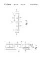
- FIG. 1is a isometric view of a field emission display according to an exemplary embodiment of the invention.
- FIG. 2is a top plan view of a column line of FIG. 1 .
- FIG. 3is a top plan view of a row line of FIG. 1 .
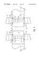
- FIG. 4is a top plan view of a row line overlying a pair of column lines.
- FIG. 5is a cross-sectional view taken along section line 5 of FIG. 4 .
- FIG. 6is a cross-sectional view taken along section line 6 of FIG. 4 .
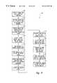
- FIG. 7is an exploded view of the component layers of the field emission display.
- FIG. 8is a flowchart of an exemplary method of forming the field emission display of FIG. 1 .
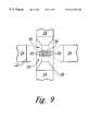
- FIG. 9is a top plan view of a row line having a necked region overlying a column line having a necked region.
- FIG. 1shows a matrix-addressable device in the form of a field mission display 10 , including a faceplate 12 and a backplate 14 .
- the faceplate 12is mounted adjacent the backplate 14 and includes a display screen formed from a glass plate 16 coated with a transparent conductive material 18 to form an anode that may be biased to approximately 1-2 kV.
- a cathodoluminescent layer 20covers the exposed surface of the anode.
- the cathodoluminescent layeremits a photon 21 in response to being struck by electrons e ⁇ .
- the emitted lightpasses through the anode and the glass plate 16 to be visible to a viewer.
- the backplate 14includes a substrate 22 on which the microelectronic structure is formed.
- the backplate 14includes a number of columns and rows selected through column lines 24 and row lines 26 .
- the column lines 24 and row lines 26are preferably formed of a conductive metal suitable for silicon fabrication processes, although they may also be fabricated from another conductive material.
- the column and row lines 24 , 26may be aluminum, tungsten, or copper.
- the column lines 24are shown as extending between the top and the bottom of the page, and the row lines 26 extending between right and left hand margins, the terms column and row are interchangeable.
- the columns lines 24may have been shown as extending across the page, while the row lines 26 may have been shown running up and down the page. Further, the column and rows lines 24 , 26 do not necessarily have to be at right angles to one another.
- Conductive emitter pads 28 of doped polysiliconmay be disposed over portions of the column lines 24 to support emitters 30 .
- the emitter pads 28electrically couple the emitters 30 to the column lines 24 .
- the polysilicon of the emitter pads 28may be appropriately doped such that the emitter pads 28 form current limiting resistors for the respective emitters 30 formed thereon.
- the polysiliconmay be doped with between approximately 10 ppm and about 100 ppm of boron.
- the polysiliconmay be doped with approximately 1 ppm and 10 ppm of phosphorous.
- the polysiliconmay be doped with approximately 1 ppm and approximately 10 ppm of arsenic.
- the emitters 30 in each sethave their bases commonly connected. While FIG. 1 shows four emitters 30 in each set, the display 10 may include any number of emitters 30 in a set. For convenience and clarity of presentation, generally only one emitter will be discussed herein. However, one skilled in the relevant art will understand that references to the emitter may refer to any number of commonly connected emitters.
- a number of conductive polysilicon extraction grid strips 32having apertures 34 formed therethrough serve as an extraction grid to excite electron emission from the emitters 30 .
- a 30-60 volt difference between the emitters 30 and the extraction grid strips 32is typically sufficient to excite electron emission.
- Openings or windows 36 formed in the row lines 26provide a free path for the flow of electrons e ⁇ from the emitters 30 to the anode 18 , as well as providing other benefits described below.
- a layer of dielectric material 27separates the column lines 24 and emitter pads 28 from the extraction grid strips 32 .
- FIG. 2shows the column line 24 as a conductive metal trace formed on the substrate 22 .
- the column line 24has a length 38 and a nominal width 40 .
- the column line 24includes a number of windows 42 spaced at intervals along the length 38 of the column line 24 .
- the windows 42are shown as rectangular, although the windows 42 may have any suitable shape and size that reduces the area of metal-metal overlap. As shown, each of the windows 42 have a length 48 and a width 50 .
- FIG. 3shows the row line 26 formed as a conductive metal trace formed on the conductive strip 32 .
- the row line 26has a length 44 and a nominal width 46 .
- the row line 26includes a number of windows 36 spaced at intervals along the length 44 of the row line 26 .
- the windows 36are shown as rectangular, although the windows 36 may also have any suitable shape and size that reduces the area of metal-metal overlap.
- each of the windows 36have a length 52 and a width 54 .
- FIG. 4shows a row line 26 overlying a pair of column lines 24 .
- the length 48 of the window 42 in the column line 24is greater than the nominal width 46 of the row line 26 .
- the length 52 of the window 36 in the row line 26is greater than the nominal width 40 of the column line 24 .
- the area of metal-metal overlap of the row line 26 and column lines 24is minimized, as indicated by the cross-hatched areas 56 .
- FIG. 5shows a cross section of the row line 26 and column lines 24 taken through section line 5 — 5 of FIG. 4 .
- FIG. 5shows the window 42 defined between legs of the column line 24 .
- FIG. 5further shows the apertures 34 in the extraction grid strip 32 aligned with the emitters 30 .
- the dielectric layer 27has been etched away around the base of the emitters 30 to further expose the emitters 30 .
- FIG. 6is a cross-sectional view of the row line 26 and column lines 24 taken through section line 6 — 6 of FIG. 4 . It may be noted that the window 36 does not appear in FIG. 6, the section being taken through one of the legs of the row line 26 .
- FIG. 7shows an exploded view of a column line 24 and row line 26 of the display 10 of FIG. 1 .
- the dielectric layer 27conforms to the column line 24 and emitter pad 28 .
- the dielectric layer 27provides support and electrical isolation to the extraction grid strip 32 .
- the window 42 in the column line 24is clearly visible in this partial, exploded view.
- FIG. 9shows a row line 26 overlying a column line 24 .
- the row line 26has a necked region 53 in the area where the row line 26 crosses the column line 24 .
- the column linehas a necked region 55 in the area where the lines cross.
- the area of overlap of the row line 26 and column lines 24is minimized, as indicated by the cross-hatched area 56 .
- FIG. 8describes an exemplary method 100 of forming the display 10 of FIG. 1 .
- a column line metal layeris deposited on the surface of the substrate 22 .
- the column line layermay be any metal or other conductor suitable for the silicon fabrication process.
- the column line metal layeris patterned to form the column lines 24 and the windows 42 . Patterning may be accomplished through conventional patterning steps, such as masking followed by a dry etch.
- an emitter pad layeris deposited on the substrate over the patterned column line layer.
- the emitter pad layeris composed of a conductive material, preferably a doped polysilicon.
- the polysiliconmay be doped to achieve a desired resistance such that the emitter pads 28 will serve as current limiting resistors for the respective emitters 30 .
- an emitter layeris deposited over the emitter pad layer.
- the emitter layercomprises a conductive material such as polysilicon and is preferably doped to have a lower resistance than the emitter pad layer.
- emitters 30are formed in the emitter layer. Emitters 30 may be formed through standard dry etching processes, although wet etching techniques and other techniques for forming emitters may be employed.
- the emitter pads 28are formed in the emitter pad layer. Again, conventional patterning steps may be suitable for emitter pad formation, such as masking and dry etching.
- a dielectric 27is deposited on the resulting substrate over the emitter pads 28 , emitters 30 , and exposed portions of the row lines 24 .
- the dielectric 27serves as a support for further deposition and as electrical insulation between the column lines 24 and the row lines 26 .
- a grid layeris deposited over the dielectric layer 27 .
- the grid layeris preferably a doped polysilicon.
- the grid layeris planarized to form apertures 34 that are self aligned to the emitters 30 .
- Chemical-mechanical planarizationmay be employed as taught in U.S. Pat. No. 5,186,670 issued Feb. 16, 1993 to Doan et al.
- a row line layeris deposited over the planarized grid layer.
- the row line layeris preferably formed from a metal that is compatible with the other silicon fabrication processing steps.
- the row line layeris patterned to form the row lines 26 and windows 36 .
- the grid layeris etched to extend the row lines 26 into the grid layer to the dielectric layer 27 . This electrically isolates each of the row lines 26 from one another.
- the dielectric 27 around the emitters 30may be etched to further expose the emitters 30 .
Landscapes
- Cathode-Ray Tubes And Fluorescent Screens For Display (AREA)
- Electrodes For Cathode-Ray Tubes (AREA)
Abstract
Description
Claims (52)
Priority Applications (1)
| Application Number | Priority Date | Filing Date | Title |
|---|---|---|---|
| US09/243,929US6417627B1 (en) | 1999-02-03 | 1999-02-03 | Matrix-addressable display with minimum column-row overlap and maximum metal line-width |
Applications Claiming Priority (1)
| Application Number | Priority Date | Filing Date | Title |
|---|---|---|---|
| US09/243,929US6417627B1 (en) | 1999-02-03 | 1999-02-03 | Matrix-addressable display with minimum column-row overlap and maximum metal line-width |
Publications (1)
| Publication Number | Publication Date |
|---|---|
| US6417627B1true US6417627B1 (en) | 2002-07-09 |
Family
ID=22920689
Family Applications (1)
| Application Number | Title | Priority Date | Filing Date |
|---|---|---|---|
| US09/243,929Expired - LifetimeUS6417627B1 (en) | 1999-02-03 | 1999-02-03 | Matrix-addressable display with minimum column-row overlap and maximum metal line-width |
Country Status (1)
| Country | Link |
|---|---|
| US (1) | US6417627B1 (en) |
Cited By (6)
| Publication number | Priority date | Publication date | Assignee | Title |
|---|---|---|---|---|
| WO2004055854A1 (en)* | 2002-12-17 | 2004-07-01 | Koninklijke Philips Electronics N.V. | Display device |
| US20110181549A1 (en)* | 2007-01-03 | 2011-07-28 | Steve Porter Hotelling | Double-sided touch-sensitive panel with shield and drive combined layer |
| US8928618B2 (en) | 2004-05-06 | 2015-01-06 | Apple Inc. | Multipoint touchscreen |
| USRE45559E1 (en) | 1997-10-28 | 2015-06-09 | Apple Inc. | Portable computers |
| US10175832B2 (en) | 2011-12-22 | 2019-01-08 | Quickstep Technologies Llc | Switched-electrode capacitive-measurement device for touch-sensitive and contactless interfaces |
| US10503328B2 (en) | 2011-06-16 | 2019-12-10 | Quickstep Technologies Llc | Device and method for generating an electrical power supply in an electronic system with a variable reference potential |
Citations (15)
| Publication number | Priority date | Publication date | Assignee | Title |
|---|---|---|---|---|
| US5194780A (en)* | 1990-06-13 | 1993-03-16 | Commissariat A L'energie Atomique | Electron source with microtip emissive cathodes |
| US5541466A (en)* | 1994-11-18 | 1996-07-30 | Texas Instruments Incorporated | Cluster arrangement of field emission microtips on ballast layer |
| US5550435A (en) | 1993-10-28 | 1996-08-27 | Nec Corporation | Field emission cathode apparatus |
| US5577944A (en) | 1994-04-29 | 1996-11-26 | Texas Instruments Incorporated | Interconnect for use in flat panel display |
| US5598057A (en) | 1995-03-13 | 1997-01-28 | Texas Instruments Incorporated | Reduction of the probability of interlevel oxide failures by minimization of lead overlap area through bus width reduction |
| US5655940A (en) | 1994-09-28 | 1997-08-12 | Texas Instruments Incorporated | Creation of a large field emission device display through the use of multiple cathodes and a seamless anode |
| US5663608A (en) | 1993-03-11 | 1997-09-02 | Fed Corporation | Field emission display devices, and field emisssion electron beam source and isolation structure components therefor |
| US5689278A (en) | 1995-04-03 | 1997-11-18 | Motorola | Display control method |
| US5727977A (en) | 1996-03-04 | 1998-03-17 | Motorola, Inc. | Process for manufacturing a field-emission device |
| US5754149A (en) | 1992-04-07 | 1998-05-19 | Micron Display Technology, Inc. | Architecture for isolating display grids in a field emission display |
| US5759078A (en)* | 1995-05-30 | 1998-06-02 | Texas Instruments Incorporated | Field emission device with close-packed microtip array |
| US5760535A (en) | 1996-10-31 | 1998-06-02 | Motorola, Inc. | Field emission device |
| US5763997A (en) | 1992-03-16 | 1998-06-09 | Si Diamond Technology, Inc. | Field emission display device |
| US5767619A (en) | 1995-12-15 | 1998-06-16 | Industrial Technology Research Institute | Cold cathode field emission display and method for forming it |
| US5814925A (en)* | 1994-09-26 | 1998-09-29 | Nec Corporation | Electron source with microtip emissive cathodes |
- 1999
- 1999-02-03USUS09/243,929patent/US6417627B1/ennot_activeExpired - Lifetime
Patent Citations (15)
| Publication number | Priority date | Publication date | Assignee | Title |
|---|---|---|---|---|
| US5194780A (en)* | 1990-06-13 | 1993-03-16 | Commissariat A L'energie Atomique | Electron source with microtip emissive cathodes |
| US5763997A (en) | 1992-03-16 | 1998-06-09 | Si Diamond Technology, Inc. | Field emission display device |
| US5754149A (en) | 1992-04-07 | 1998-05-19 | Micron Display Technology, Inc. | Architecture for isolating display grids in a field emission display |
| US5663608A (en) | 1993-03-11 | 1997-09-02 | Fed Corporation | Field emission display devices, and field emisssion electron beam source and isolation structure components therefor |
| US5550435A (en) | 1993-10-28 | 1996-08-27 | Nec Corporation | Field emission cathode apparatus |
| US5577944A (en) | 1994-04-29 | 1996-11-26 | Texas Instruments Incorporated | Interconnect for use in flat panel display |
| US5814925A (en)* | 1994-09-26 | 1998-09-29 | Nec Corporation | Electron source with microtip emissive cathodes |
| US5655940A (en) | 1994-09-28 | 1997-08-12 | Texas Instruments Incorporated | Creation of a large field emission device display through the use of multiple cathodes and a seamless anode |
| US5541466A (en)* | 1994-11-18 | 1996-07-30 | Texas Instruments Incorporated | Cluster arrangement of field emission microtips on ballast layer |
| US5598057A (en) | 1995-03-13 | 1997-01-28 | Texas Instruments Incorporated | Reduction of the probability of interlevel oxide failures by minimization of lead overlap area through bus width reduction |
| US5689278A (en) | 1995-04-03 | 1997-11-18 | Motorola | Display control method |
| US5759078A (en)* | 1995-05-30 | 1998-06-02 | Texas Instruments Incorporated | Field emission device with close-packed microtip array |
| US5767619A (en) | 1995-12-15 | 1998-06-16 | Industrial Technology Research Institute | Cold cathode field emission display and method for forming it |
| US5727977A (en) | 1996-03-04 | 1998-03-17 | Motorola, Inc. | Process for manufacturing a field-emission device |
| US5760535A (en) | 1996-10-31 | 1998-06-02 | Motorola, Inc. | Field emission device |
Cited By (14)
| Publication number | Priority date | Publication date | Assignee | Title |
|---|---|---|---|---|
| USRE45559E1 (en) | 1997-10-28 | 2015-06-09 | Apple Inc. | Portable computers |
| USRE46548E1 (en) | 1997-10-28 | 2017-09-12 | Apple Inc. | Portable computers |
| US20070052337A1 (en)* | 2002-12-17 | 2007-03-08 | Van Der Poel Willibrordus A J | Display device |
| WO2004055854A1 (en)* | 2002-12-17 | 2004-07-01 | Koninklijke Philips Electronics N.V. | Display device |
| US8928618B2 (en) | 2004-05-06 | 2015-01-06 | Apple Inc. | Multipoint touchscreen |
| US9075491B2 (en) | 2007-01-03 | 2015-07-07 | Apple Inc. | Double-sided touch-sensitive panel with shield and drive combined layer |
| US8884890B2 (en) | 2007-01-03 | 2014-11-11 | Apple Inc. | Double-sided touch-sensitive panel with shield and drive combined layer |
| US9465502B2 (en) | 2007-01-03 | 2016-10-11 | Apple Inc. | Double-sided touch-sensitive panel with shield and drive combined layer |
| US20110181549A1 (en)* | 2007-01-03 | 2011-07-28 | Steve Porter Hotelling | Double-sided touch-sensitive panel with shield and drive combined layer |
| US9836160B2 (en) | 2007-01-03 | 2017-12-05 | Apple Inc. | Double-sided touch-sensitive panel with shield and drive combined layer |
| US10474287B2 (en) | 2007-01-03 | 2019-11-12 | Apple Inc. | Double-sided touch-sensitive panel with shield and drive combined layer |
| US11112904B2 (en) | 2007-01-03 | 2021-09-07 | Apple Inc. | Double-sided touch-sensitive panel with shield and drive combined layer |
| US10503328B2 (en) | 2011-06-16 | 2019-12-10 | Quickstep Technologies Llc | Device and method for generating an electrical power supply in an electronic system with a variable reference potential |
| US10175832B2 (en) | 2011-12-22 | 2019-01-08 | Quickstep Technologies Llc | Switched-electrode capacitive-measurement device for touch-sensitive and contactless interfaces |
Similar Documents
| Publication | Publication Date | Title |
|---|---|---|
| EP0985220B1 (en) | Fabrication of electron-emitting device having ladder-like emitter electrode | |
| US5621272A (en) | Field emission device with over-etched gate dielectric | |
| US5780318A (en) | Cold electron emitting device and method of manufacturing same | |
| US5920148A (en) | Field emission display cell structure | |
| US5710483A (en) | Field emission device with micromesh collimator | |
| US5711694A (en) | Field emission device with lattice vacancy, post-supported gate | |
| US5897414A (en) | Technique for increasing manufacturing yield of matrix-addressable device | |
| US5759078A (en) | Field emission device with close-packed microtip array | |
| US5920151A (en) | Structure and fabrication of electron-emitting device having focus coating contacted through underlying access conductor | |
| US6417627B1 (en) | Matrix-addressable display with minimum column-row overlap and maximum metal line-width | |
| US6045426A (en) | Method to manufacture field emission array with self-aligned focus structure | |
| US5932962A (en) | Electron emitter elements, their use and fabrication processes therefor | |
| US5502347A (en) | Electron source | |
| EP0706198B1 (en) | Redundant conductor electron source | |
| US6210246B1 (en) | Method for making an electron source with microtips, with self-aligned focusing grid | |
| US5630741A (en) | Fabrication process for a field emission display cell structure | |
| US6387718B2 (en) | Field emission arrays and method of fabricating emitter tips and corresponding resistors thereof with a single mask | |
| JPH0831347A (en) | Microchip radiation cathode electron source | |
| US5994834A (en) | Conductive address structure for field emission displays | |
| US20070024178A1 (en) | Field emission device having insulated column lines and method of manufacture | |
| US6172455B1 (en) | Flat display screen including a cathode having electron emission microtips associated with a grid for extracting electrons from the microtips | |
| US5633120A (en) | Method for achieving anode stripe delineation from an interlevel dielectric etch in a field emission device | |
| US6144351A (en) | Field emitter display baseplate and method of fabricating same | |
| US5920296A (en) | Flat screen having individually dipole-protected microdots | |
| US6010917A (en) | Electrically isolated interconnects and conductive layers in semiconductor device manufacturing |
Legal Events
| Date | Code | Title | Description |
|---|---|---|---|
| AS | Assignment | Owner name:MICRON TECHNOLOGY, INC., IDAHO Free format text:ASSIGNMENT OF ASSIGNORS INTEREST;ASSIGNOR:DERRAA, AMMAR;REEL/FRAME:009770/0405 Effective date:19990127 | |
| STCF | Information on status: patent grant | Free format text:PATENTED CASE | |
| FPAY | Fee payment | Year of fee payment:4 | |
| FPAY | Fee payment | Year of fee payment:8 | |
| FPAY | Fee payment | Year of fee payment:12 | |
| AS | Assignment | Owner name:U.S. BANK NATIONAL ASSOCIATION, AS COLLATERAL AGENT, CALIFORNIA Free format text:SECURITY INTEREST;ASSIGNOR:MICRON TECHNOLOGY, INC.;REEL/FRAME:038669/0001 Effective date:20160426 Owner name:U.S. BANK NATIONAL ASSOCIATION, AS COLLATERAL AGEN Free format text:SECURITY INTEREST;ASSIGNOR:MICRON TECHNOLOGY, INC.;REEL/FRAME:038669/0001 Effective date:20160426 | |
| AS | Assignment | Owner name:MORGAN STANLEY SENIOR FUNDING, INC., AS COLLATERAL AGENT, MARYLAND Free format text:PATENT SECURITY AGREEMENT;ASSIGNOR:MICRON TECHNOLOGY, INC.;REEL/FRAME:038954/0001 Effective date:20160426 Owner name:MORGAN STANLEY SENIOR FUNDING, INC., AS COLLATERAL Free format text:PATENT SECURITY AGREEMENT;ASSIGNOR:MICRON TECHNOLOGY, INC.;REEL/FRAME:038954/0001 Effective date:20160426 | |
| AS | Assignment | Owner name:U.S. BANK NATIONAL ASSOCIATION, AS COLLATERAL AGENT, CALIFORNIA Free format text:CORRECTIVE ASSIGNMENT TO CORRECT THE REPLACE ERRONEOUSLY FILED PATENT #7358718 WITH THE CORRECT PATENT #7358178 PREVIOUSLY RECORDED ON REEL 038669 FRAME 0001. ASSIGNOR(S) HEREBY CONFIRMS THE SECURITY INTEREST;ASSIGNOR:MICRON TECHNOLOGY, INC.;REEL/FRAME:043079/0001 Effective date:20160426 Owner name:U.S. BANK NATIONAL ASSOCIATION, AS COLLATERAL AGEN Free format text:CORRECTIVE ASSIGNMENT TO CORRECT THE REPLACE ERRONEOUSLY FILED PATENT #7358718 WITH THE CORRECT PATENT #7358178 PREVIOUSLY RECORDED ON REEL 038669 FRAME 0001. ASSIGNOR(S) HEREBY CONFIRMS THE SECURITY INTEREST;ASSIGNOR:MICRON TECHNOLOGY, INC.;REEL/FRAME:043079/0001 Effective date:20160426 | |
| AS | Assignment | Owner name:JPMORGAN CHASE BANK, N.A., AS COLLATERAL AGENT, ILLINOIS Free format text:SECURITY INTEREST;ASSIGNORS:MICRON TECHNOLOGY, INC.;MICRON SEMICONDUCTOR PRODUCTS, INC.;REEL/FRAME:047540/0001 Effective date:20180703 Owner name:JPMORGAN CHASE BANK, N.A., AS COLLATERAL AGENT, IL Free format text:SECURITY INTEREST;ASSIGNORS:MICRON TECHNOLOGY, INC.;MICRON SEMICONDUCTOR PRODUCTS, INC.;REEL/FRAME:047540/0001 Effective date:20180703 | |
| AS | Assignment | Owner name:MICRON TECHNOLOGY, INC., IDAHO Free format text:RELEASE BY SECURED PARTY;ASSIGNOR:U.S. BANK NATIONAL ASSOCIATION, AS COLLATERAL AGENT;REEL/FRAME:047243/0001 Effective date:20180629 | |
| AS | Assignment | Owner name:MICRON TECHNOLOGY, INC., IDAHO Free format text:RELEASE BY SECURED PARTY;ASSIGNOR:MORGAN STANLEY SENIOR FUNDING, INC., AS COLLATERAL AGENT;REEL/FRAME:050937/0001 Effective date:20190731 | |
| AS | Assignment | Owner name:MICRON SEMICONDUCTOR PRODUCTS, INC., IDAHO Free format text:RELEASE BY SECURED PARTY;ASSIGNOR:JPMORGAN CHASE BANK, N.A., AS COLLATERAL AGENT;REEL/FRAME:051028/0001 Effective date:20190731 Owner name:MICRON TECHNOLOGY, INC., IDAHO Free format text:RELEASE BY SECURED PARTY;ASSIGNOR:JPMORGAN CHASE BANK, N.A., AS COLLATERAL AGENT;REEL/FRAME:051028/0001 Effective date:20190731 |