US6417094B1 - Dual-damascene interconnect structures and methods of fabricating same - Google Patents
Dual-damascene interconnect structures and methods of fabricating sameDownload PDFInfo
- Publication number
- US6417094B1 US6417094B1US09/224,339US22433998AUS6417094B1US 6417094 B1US6417094 B1US 6417094B1US 22433998 AUS22433998 AUS 22433998AUS 6417094 B1US6417094 B1US 6417094B1
- Authority
- US
- United States
- Prior art keywords
- dielectric
- barrier layer
- metal
- layer
- trench
- Prior art date
- Legal status (The legal status is an assumption and is not a legal conclusion. Google has not performed a legal analysis and makes no representation as to the accuracy of the status listed.)
- Expired - Lifetime
Links
Images


Classifications
- H—ELECTRICITY
- H01—ELECTRIC ELEMENTS
- H01L—SEMICONDUCTOR DEVICES NOT COVERED BY CLASS H10
- H01L21/00—Processes or apparatus adapted for the manufacture or treatment of semiconductor or solid state devices or of parts thereof
- H01L21/70—Manufacture or treatment of devices consisting of a plurality of solid state components formed in or on a common substrate or of parts thereof; Manufacture of integrated circuit devices or of parts thereof
- H01L21/71—Manufacture of specific parts of devices defined in group H01L21/70
- H01L21/768—Applying interconnections to be used for carrying current between separate components within a device comprising conductors and dielectrics
- H01L21/76801—Applying interconnections to be used for carrying current between separate components within a device comprising conductors and dielectrics characterised by the formation and the after-treatment of the dielectrics, e.g. smoothing
- H01L21/76829—Applying interconnections to be used for carrying current between separate components within a device comprising conductors and dielectrics characterised by the formation and the after-treatment of the dielectrics, e.g. smoothing characterised by the formation of thin functional dielectric layers, e.g. dielectric etch-stop, barrier, capping or liner layers
- H01L21/76831—Applying interconnections to be used for carrying current between separate components within a device comprising conductors and dielectrics characterised by the formation and the after-treatment of the dielectrics, e.g. smoothing characterised by the formation of thin functional dielectric layers, e.g. dielectric etch-stop, barrier, capping or liner layers in via holes or trenches, e.g. non-conductive sidewall liners
- H—ELECTRICITY
- H01—ELECTRIC ELEMENTS
- H01L—SEMICONDUCTOR DEVICES NOT COVERED BY CLASS H10
- H01L21/00—Processes or apparatus adapted for the manufacture or treatment of semiconductor or solid state devices or of parts thereof
- H01L21/70—Manufacture or treatment of devices consisting of a plurality of solid state components formed in or on a common substrate or of parts thereof; Manufacture of integrated circuit devices or of parts thereof
- H01L21/71—Manufacture of specific parts of devices defined in group H01L21/70
- H01L21/768—Applying interconnections to be used for carrying current between separate components within a device comprising conductors and dielectrics
- H01L21/76801—Applying interconnections to be used for carrying current between separate components within a device comprising conductors and dielectrics characterised by the formation and the after-treatment of the dielectrics, e.g. smoothing
- H01L21/76802—Applying interconnections to be used for carrying current between separate components within a device comprising conductors and dielectrics characterised by the formation and the after-treatment of the dielectrics, e.g. smoothing by forming openings in dielectrics
- H01L21/76807—Applying interconnections to be used for carrying current between separate components within a device comprising conductors and dielectrics characterised by the formation and the after-treatment of the dielectrics, e.g. smoothing by forming openings in dielectrics for dual damascene structures
- H01L21/76808—Applying interconnections to be used for carrying current between separate components within a device comprising conductors and dielectrics characterised by the formation and the after-treatment of the dielectrics, e.g. smoothing by forming openings in dielectrics for dual damascene structures involving intermediate temporary filling with material
- H—ELECTRICITY
- H01—ELECTRIC ELEMENTS
- H01L—SEMICONDUCTOR DEVICES NOT COVERED BY CLASS H10
- H01L2221/00—Processes or apparatus adapted for the manufacture or treatment of semiconductor or solid state devices or of parts thereof covered by H01L21/00
- H01L2221/10—Applying interconnections to be used for carrying current between separate components within a device
- H01L2221/1005—Formation and after-treatment of dielectrics
- H01L2221/101—Forming openings in dielectrics
- H01L2221/1015—Forming openings in dielectrics for dual damascene structures
- H01L2221/1031—Dual damascene by forming vias in the via-level dielectric prior to deposition of the trench-level dielectric
Definitions
- the present inventionrelates, generally, to methods and structures for improving the reliability and manufacturability of multilevel interconnects in integrated circuits and, more particularly, to a dual damascene process with barrier enhancement at the via sidewalls and improved capability for fabricating high aspect ratio interconnect structures.
- a low-k dielectricis a dielectric material which exhibits a dielectric constant substantially less than conventional dielectric materials such as silicon dioxide, silicon nitride, and silicon oxynitride.
- Silicon dioxidefor example, has a dielectric constant of about 4.0.
- Copperis desirable in that its conductivity is relatively high and it is less susceptible to electromigration failure than many metals (for example, aluminum).
- CMPChemical-Mechanical Polishing
- a resinous polishing pade.g., a polyurethane pad
- a mechanically and chemically active slurryWhen pressure is applied between the polishing pad and the wafer being polished, mechanical stresses are concentrated on the exposed edges of the adjoining cells in the cellular pad.
- a fabrication method which employs CMP techniques and which addresses many of the above concernsis the so-called “damascene” process.
- Damasceningacquired its name from an ornamental technique, generally attributed to metal-workers in ancient Damascus, which involved scribing or incising patterns into steel (most often swords) then filling the resulting grooves with gold or silver prior to final polish.
- the modern semiconductor analog of this processinvolves, in the broadest sense, forming patterns in a dielectric layer, filling the resulting pattern with interconnect metal, then polishing away the excess metal on the wafer surface and leaving inlaid interconnect metal features.
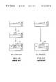
- a single damascene processinvolves making contact to a lower level conductor 102 (formed, for example, on substrate 107 ) by patterning dielectric layer 106 and forming a conductive plug 104 in dielectric layer 106 , then patterning a second dielectric layer 110 and forming the actual interconnect wiring metallization 108 in patterned dielectric layer 110 .
- the interconnect wiring 108 and plug 104are formed by patterning both the via and the trench patterns into dielectric 106 , then filling them simultaneously with metal.
- the dual damascene processoffers the advantages of process simplification and lower manufacturing cost.
- Cuinterconnect metal in dual damascene IC devices gives rise to many difficulties and challenges.
- coppertends to migrate or diffuse into the silicon dioxide, where it acts to increase leakage currents or actually short-out adjacent conductors.
- the devicewill generally malfunction in some manner. This has motivated the semiconductor industry to form diffusion barriers around any copper conductors present in the structure.
- the inner surfacesi.e., the bottom and sides of the via and trench
- Ti, TiN, Ta, TaN, WNanother adequate barrier metal.
- TiNwhich is popular as a barrier layer in Al/W interconnect structures, is generally unsatisfactory for use with advanced copper interconnect structures.
- Ta and/or TaNas a barrier metal has become quite popular.
- Ta and TaNmay be deposited by physical vapor deposition (PVD) or chemical vapor deposition (CVD).
- PVDphysical vapor deposition
- CVD TaN/Tasuffers from low deposition rate and high deposition temperature (i.e., temperatures greater than 500° C.). These high temperatures and low deposition rates are incompatible with current interconnect processes as well as future processes incorporating low-k dielectrics.
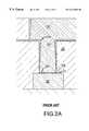
- high aspect ratio interconnectsare prone to poor step coverage of the barrier layer at the sidewall of the vias. More particularly, referring now to FIG.
- barrier 224typically comprises Ta or TaN.
- barrier layer 224is significantly less near the lower portion of the via sidewall ( 226 ). As a result, these regions are particularly susceptible to Cu migration ( 228 ).
- a layer of copper 230may be deposited along the sidewalls near the bottom of the via prior to formation of metal barrier 224 . That is, copper (from copper conductor 102 ) tends to be sputtered along the sidewalls (1) during the silicon nitride etch used to open the via connection to conductor 102 ; and (2) during the sputter-clean of conductor 102 just prior to deposition of metal barrier 224 . As mentioned above, this copper may then diffuse into surrounding structures, leading to significant reliability problems.
- etching of high aspect ratio (AR) dual-damascene featuresis itself very challenging.
- etching dielectricsis generally easier than etching metals (thus the desirability of damascene processes)
- etching the dual damascene structures of very high AR featuresleads to fabrication difficulties.
- An interconnect fabrication process and structure in accordance with the present inventionovercomes limitations of the prior art by providing barrier enhancement at the via sidewalls and easing the fabrication of high aspect ratio dual-damascene interconnect structures.
- a via structureis patterned into the via dielectric first.
- a dielectric barrierfor example, anisotropically etched silicon nitride
- a metal barrierfor example, Ta/TaN.
- the effective barrier thickness along the bottom of the via sidewallsis increased, eliminating the structure's susceptibility to metal migration.
- the absence of dielectric barrier along the interconnect trench sidewallsleads to low interconnect resistance and low interconnect capacitance.
- the present inventionalso provides an improved fabrication method for obtaining high aspect ratio dual damascene interconnect structures.
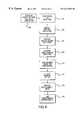
- FIG. 1Ais a diagrammatic illustration of a conventional single damascene interconnect process
- FIG. 1Bis a diagrammatic illustration of a conventional dual-damascene interconnect process
- FIGS. 2A-2Bshow a cross-sectional illustration of a prior art via, depicting its susceptibility to copper migration
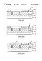
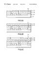
- FIGS. 3A-3Hshows cross-sectional illustrations of a method of forming dual-damascene structures by first patterning vias in the via dielectric in accordance with various aspects of the present invention
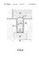
- FIG. 4shows a cross-sectional illustration of an improved barrier along via sidewalls in accordance with the present invention
- FIG. 5is a flowchart depicting an exemplary processing method in accordance with the present invention.
- FIGS. 6A-6Fshows cross-sectional illustrations of an alternative method of forming dual-damascene interconnects by first forming vias into the via dielectric in accordance with the present invention
- FIGS. 7A-7Fshows cross-sectional illustrations of an alternative method of forming dual-damascene interconnects by first forming vias in via dielectric in accordance with the present invention, wherein the lower conductor metal is covered by a barrier dielectric;
- FIG. 8shows a cross-sectional illustration of an improved barrier along via sidewalls in accordance with the present invention.
- An interconnect fabrication process in accordance with various aspects of the present inventionprovides barrier enhancement at the via sidewall and improved capability to fabricate high aspect ratio dual damascene structures. While the manner in which the present invention addresses limitations of the prior art are discussed in detail below, in general, referring momentarily to FIG. 4, a via structure 400 formed within a dielectric 309 (linking metal pattern 326 and conductor 304 ), is lined with a barrier dielectric layer 314 (for example, silicon nitride) prior to deposition of metal barrier 328 onto the dual damascene structure. As a result, the effective barrier thickness along the bottom of the via ( 410 ) as well as the top of the via ( 412 ) is sufficient to eliminate the structure's susceptibility to Cu migration.
- a barrier dielectric layer 314for example, silicon nitride
- FIG. 5an exemplary method of practicing the present invention will now be described in conjunction with the cross-sectional diagrams shown in FIG. 3 . It should be understood that the exemplary process illustrated may include more or less steps or may be performed in the context of a larger processing scheme. Furthermore, the various flowcharts presented in the drawing figures are not to be construed as limiting the order in which the individual process steps may be performed.
- the first level conductor, contact diffusion area, or the likeis obtained.
- a first metal wiring pattern 304 and a substantially planar via dielectric 309are formed on substrate 302 (see FIG. 3 A).
- This stepmay be performed through a variety of conventional techniques (e.g., CMP of deposited dielectric or a damascene process).
- Conductor 304suitably consists of a layer or layers of various conductive materials, including, for example, titanium, titanium nitride, tantalum, tantalum nitride, tungsten nitride, aluminum, aluminum-copper alloys, gold, copper, silver, tungsten, or any other suitable conductive material.
- conductor 304may consist of a previous diffused contact region in a semiconductor, a silicon contact, a previous interconnect structure, or any other layer or region to which an interconnect may be formed.
- Dielectric 309suitably comprises silicon dioxide, silicon oxynitride, silicon nitride, or any of the various low-k dielectric materials.
- via dielectric layer 309comprises a plasma-enhanced CVD (PECVD) layer of silicon dioxide approximately 0.4 ⁇ m-1.0 ⁇ m thick above conductor 304 , although other materials and thicknesses may be used.
- PECVDplasma-enhanced CVD
- a thin dielectric cap layer(not shown in FIG. 3A) is deposited on top of layer 309 .
- This thin cap layere.g., silicon dioxide or silicon nitride
- Substrate 302includes any suitable substrate material upon which or within which semiconductor devices may be formed. Suitable materials for substrate 302 include, for example, group IV semiconductors (i.e., Si, Ge, and SiGe), group III-V semiconductors (i.e., GaAs, InAs, and AlGaAs), and other less-conventional materials, such as SiC, diamond, and sapphire. Substrate 302 may comprise single crystal material, or may comprise one or more polycrystalline or amorphous epitaxial layer formed on a suitable base material. It will be appreciated that substrate 302 may also comprise various devices incorporated into a semiconductor material as well as interconnect structures consisting of conductive paths and various dielectrics for isolating these conductive paths.
- group IV semiconductorsi.e., Si, Ge, and SiGe
- group III-V semiconductorsi.e., GaAs, InAs, and AlGaAs
- SiCsilicon carbide
- substrate 302may comprise single crystal material, or may comprise
- vias 312are formed in via dielectric 309 (FIGS. 3 B- 3 C).
- Thismay be accomplished using a variety of known lithographic techniques, for example, conventional optical lithography (including, for example, I-line and deep-UV), X-ray, E-beam lithography, and plasma etch techniques.
- a layer of photoresist 310is deposited and patterned using a suitable lithographic method.
- dielectric 309is suitably etched (e.g., using a dry plasma etch) to form the via hole pattern, and the photoresist layer 310 is removed using, for example, an oxygen-based or hydrogen-based plasma.
- barrier dielectric 314is deposited within vias 312 and along the topside of via dielectric 309 .
- this layerwill ultimately act as an additional barrier along the inner walls of the vias (i.e., barrier dielectric 314 in FIG. 4 ).
- barrier dielectric 314comprises a silicon nitride layer having a thickness of about 100-1000 ⁇ . This layer is suitably formed using a conventional CVD process.
- barrier dielectric layer 314may be formed by exposure of the structure to an environment wherein all or part of the via dielectric 309 exposed is substantially transformed to a barrier dielectric.
- dielectric layer 309comprises silicon dioxide
- a conventional nitrogen plasma processmay be used to transform the exposed via dielectric 309 surface into a thin layer of silicon nitride.
- a dielectric layer 316is then deposited over barrier dielectric 314 .
- layer 316comprises a CVD layer of silicon dioxide approximately 0.2-1.0 microns thick. As shown schematically in FIG. 3D, dielectric 316 will typically fill a portion of vias 312 (and might also be deposited along the sidewalls and bottom of via 312 ).
- wiring dielectric layer (or “trench dielectric”) 316is patterned in accordance with the desired interconnect wiring pattern (FIGS. 3 E- 3 F). As described above in connection with layer 309 , this may be accomplished using a variety of known lithographic techniques, for example, conventional optical lithography (including, for example, I-line and deep-UV), X-ray, E-beam lithography, and plasma etch techniques. In a preferred embodiment, a layer of photoresist 318 is deposited and patterned (pattern 320 ) using a suitable lithographic method.
- dielectric 316(including the dielectric material which partially fills vias 312 ) is suitably etched (e.g., using a dry plasma etch), and photoresist layer 318 is removed using, for example, an oxygen-based or hydrogen-based plasma.
- layer 314effectively acts as an etch stop. That is, the etch process is chosen such that the materials used for layers 316 and 314 exhibit a differential etch rate.
- etching of silicon dioxide, silicon nitride, and the likesee, for example, Givens et al., Selective dry etching in a high density plasma for 0.5 ⁇ m complementary metal - oxide - semiconductor technology , J. V ac. S ci. T echnol. B, p. 427 (January/February 1994), hereby incorporated by reference.
- FIG. 3Fsubstantially all dielectric material 316 inside the via holes is removed.
- dielectric barrier 314is etched such that the dielectric barrier is substantially removed at the bottom of the vias and remains along the sidewalls ( 324 ) of the vias, yet is substantially removed from the top of dielectric 309 (Step 510 ).
- Thisis preferably accomplished using an anisotropic etching process.
- this etchis selective to dielectric 309 —i.e., the etch will stop or slow when it exposes dielectric 309 .
- a conventional anisotropic etching process used to form the spacer during the fabrication of CMOS transistorsmay be used. This provides the desired anisotropic etch of silicon nitride and etch selectivity to silicon dioxide. In one embodiment, approximately 30% to 50% of the silicon nitride remains along sidewalls 324 of the vias.
- a barrier metal 328is suitably deposited within vias 312 and wiring pattern 322 , followed by deposition of bulk metal 326 (FIG. 3 H).
- Barrier layer 328may consist of a variety of materials, for example, titanium, titanium nitride, tantalum, tantalum nitride, tungsten nitride, TiSiN, TaSiN, CoWP, tungsten, and/or molybdenum.
- the adhesion/barrier layersuitably comprises a Ta/TaN film approximately 50 ⁇ -300 ⁇ deposited using ionized metal plasma (IMP) or hollow cathode magnetron (HCM) sputtering.
- IMPionized metal plasma
- HCMhollow cathode magnetron
- metal barrier 328 and dielectric barrier 314provides a particularly advantageous barrier to prevent copper migration.
- barrier dielectric 314tends to taper near the top of the via (due to the anisotropic etching step)
- barrier metal 328tends to taper near the bottom of the via ( 410 ).
- the resulting structureis significantly more robust than prior art structures.
- a suitable adhesion/wetting/barrier metal layermay be deposited within trenches 322 and vias 312 (i.e., in addition to or as part of layer 328 ).
- adhesion layersgenerally assist in strengthening the bond between metal and dielectric layers, and barrier layers provide a barrier to prevent the migration or alloying of one material into another (for example, copper diffusion into silicon).
- Wetting layerspromote metal fill in high aspect-ratio features.
- a single materialmay exhibit one or more of these properties in a particular context.
- the terms “adhesion layer”, “wetting layer”, and “barrier layer” as used hereinare not meant to be limiting.
- metal 326suitably consists of a layer or layers of various conductive materials, including, for example, titanium, titanium nitride, tantalum, tantalum nitride, tungsten nitride, aluminum, aluminum-copper alloys, gold, copper, silver, tungsten, or any other suitable conductive material.
- metal 326comprises copper deposited using electrochemical deposition (or “electroplating”). Alternatively, other deposition techniques such as CVD may be used. Many commercial tools are suitable for the copper-electroplating step, including, for example, the EQUINOX tool manufactured by Semitool and the SABRE tool manufactured by Novellus. Such a system suitably employs a CuSO 4 -based bath at room temperature using a DC or pulse current waveform control.
- a copper seed layeris deposited prior to forming bulk copper layer 326 .
- the seed layerhelps in delivering electron current uniformly on the wafer for initiation of uniform electroplating.
- the copper seed layeris suitably formed using ion-metal plasma (IMP) or hollow-cathode-magnetron (HCM) sputtering deposition for better bottom and sidewall coverage.
- IMPion-metal plasma
- HCMhollow-cathode-magnetron
- the copper seed layercan be deposited by other PVD techniques or CVD techniques.
- the copper seed layeris approximately 500 ⁇ -2000 ⁇ thick.
- Step 516the excess metal 330 (not shown) and corresponding adhesion/wetting/barrier layers on the field are removed, forming the desired interconnect wiring (FIG. 3 H).
- this stepis performed using a conventional CMP process.
- a suitable CMP slurryconsists, for example, of any one of the following combinations: hydrogen peroxide and alumina; ammonium hydroxide and alumina; or nitric acid and alumina.
- This processcan be performed using a conventional polyurethane pad, for example, the IC1000 and IC1400 pads manufactured by Rodel.
- dielectric barrier layeris formed along the via sidewalls but not along the wiring trench sidewalls. This is achieved by etching via holes into via dielectric first and then depositing barrier dielectric before the trench dielectric is deposited.
- barrier dielectricalong the wiring trench sidewalls leads to low interconnect wiring resistance (as more physical trench space is filled with conductive metal) and low interconnect wiring capacitance (because the typical barrier dielectric has a relatively high dielectric constant).
- This approachprovides yet another advantage, i.e., improved capability to etch dual damascene structures with very high aspect ratios as compared to well known “trench-first”, “via-first”, and “middle-first” dual damascene approaches.
- the via holesare partially filled with dielectric material after the trench dielectric is deposited, removal of the dielectric material in the via holes during the trench etch step is much easier than with the trench-first and middle-first approaches because there is substantially less dielectric material deposited in the via holes in the present approach.
- the present inventioncan be practiced even in cases where barrier enhancement along the via sidewall is not required, for example, in aluminum dual damascene processes or where a more conformal metal barrier layer can be deposited along the via sidewalls.
- etching of the barrier dielectric layer(Step 510 , FIGS. 3F-3G) may be performed either isotropically or anisotropically.
- FIG. 6,illustrates an alternative method of forming vias in dual damascene structures in accordance the present invention.
- FIGS. 6A-6Fdepict a modification of the process shown in FIG. 5, minus steps 504 and 510 .
- the resulting processinvolves formation of via dielectric 309 and an etch stop layer 315 (i.e., silicon nitride) over conductor 304 (Step 500 ); formation of vias 312 into etch stop 315 and via dielectric 309 (Step 502 , FIG. 6 A); deposition of trench dielectric layer 316 (Step 506 , FIG. 6 B); patterning of dielectric layer 316 to form trenches 322 (Step 508 , FIGS.
- etch stop layer 315i.e., silicon nitride
- etch-stop 315acts to protect dielectric layer 309 when the dielectric material in the via holes is etched away; etching away etch-stop dielectric 315 at the bottom of the trenches (selective to layer 309 ) to reduce interlayer capacitance (FIG. 6 E); and deposition of barrier metal 328 and bulk metal 326 followed by CMP (Steps 512 - 516 , FIG. 6 F).
- FIGS. 7A-7Fshow an alternate embodiment of the present invention which further includes use of cap barrier layer 305 (e.g., silicon nitride) over copper conductor 304 (or other suitable metals).
- This structuremay be formed in accordance with the method described above in conjunction with FIG. 3 .
- layer 305remains after via etch to prevent Cu oxidation in subsequent processing steps.
- the portion at the bottom of the viasis removed later with the dielectric barrier at the via bottom by the end anisotropic and selective etch (see FIGS. 7 D- 7 E), such that the resulting dielectric barrier remains on the via sidewalls, and the vias are opened.
- the current approach with barrier enhancementalso prevents migration of extraneous sputtered copper on the via sidewall. That is, as described above in conjunction with FIG. 2B, copper from, for example, a copper conductor 102 , tends to be sputtered along the sidewalls during the silicon nitride etch used to open the via connection to the conductor (FIGS. 7 D- 7 E), and during sputter-clean of the conductor just prior to deposition of the metal barrier. As shown in FIGS. 7D-7E, the present invention provides a dielectric barrier along the sidewall before the bottom of the vias are opened to expose the conductor. Referring to FIG. 8, methods in accordance with the present invention result in a dielectric barrier 314 between copper 230 and dielectric 309 . Thus, copper 230 is effectively trapped between metal barrier 328 and dielectric barrier 314 and cannot therefore migrate into dielectric 309 .
- interconnect levelsmay be fabricated using methods in accordance with the present invention. More particularly, it is possible to repeat the methods presented above in order to build one or more subsequent dual damascene interconnect structures upon the existing structure.
Landscapes
- Engineering & Computer Science (AREA)
- Physics & Mathematics (AREA)
- Condensed Matter Physics & Semiconductors (AREA)
- General Physics & Mathematics (AREA)
- Manufacturing & Machinery (AREA)
- Computer Hardware Design (AREA)
- Microelectronics & Electronic Packaging (AREA)
- Power Engineering (AREA)
- Internal Circuitry In Semiconductor Integrated Circuit Devices (AREA)
Abstract
Description
Claims (15)
Priority Applications (3)
| Application Number | Priority Date | Filing Date | Title |
|---|---|---|---|
| US09/224,339US6417094B1 (en) | 1998-12-31 | 1998-12-31 | Dual-damascene interconnect structures and methods of fabricating same |
| PCT/US1999/031052WO2000039849A1 (en) | 1998-12-31 | 1999-12-28 | Dual-damascene interconnect structures and methods of fabricating same |
| TW088123379ATW441015B (en) | 1998-12-31 | 2000-01-10 | Dual-damascene interconnect structures and methods for fabricating same |
Applications Claiming Priority (1)
| Application Number | Priority Date | Filing Date | Title |
|---|---|---|---|
| US09/224,339US6417094B1 (en) | 1998-12-31 | 1998-12-31 | Dual-damascene interconnect structures and methods of fabricating same |
Publications (1)
| Publication Number | Publication Date |
|---|---|
| US6417094B1true US6417094B1 (en) | 2002-07-09 |
Family
ID=22840233
Family Applications (1)
| Application Number | Title | Priority Date | Filing Date |
|---|---|---|---|
| US09/224,339Expired - LifetimeUS6417094B1 (en) | 1998-12-31 | 1998-12-31 | Dual-damascene interconnect structures and methods of fabricating same |
Country Status (3)
| Country | Link |
|---|---|
| US (1) | US6417094B1 (en) |
| TW (1) | TW441015B (en) |
| WO (1) | WO2000039849A1 (en) |
Cited By (52)
| Publication number | Priority date | Publication date | Assignee | Title |
|---|---|---|---|---|
| US20020109233A1 (en)* | 2000-01-18 | 2002-08-15 | Micron Technology, Inc. | Process for providing seed layers for integrated circuit metallurgy |
| US20020177302A1 (en)* | 2000-01-18 | 2002-11-28 | Micron Technology, Inc. | Structures and methods to enhance copper metallization |
| US6509267B1 (en)* | 2001-06-20 | 2003-01-21 | Advanced Micro Devices, Inc. | Method of forming low resistance barrier on low k interconnect with electrolessly plated copper seed layer |
| US20030075752A1 (en)* | 2001-10-19 | 2003-04-24 | Nec Corporation | Semiconductor device and method for manufacturing the same |
| US6579786B2 (en)* | 1999-05-17 | 2003-06-17 | Infineon Technologies Ag | Method for depositing a two-layer diffusion barrier |
| US6607978B2 (en)* | 1999-09-21 | 2003-08-19 | Nec Electronics Corporation | Method of making a semiconductor device with alloy film between barrier metal and interconnect |
| US6646345B2 (en)* | 1999-05-26 | 2003-11-11 | International Business Machines Corporation | Method for forming Co-W-P-Au films |
| US20040048459A1 (en)* | 2002-04-11 | 2004-03-11 | Robert Patti | Interlocking conductor method for bonding wafers to produce stacked integrated circuits |
| US20040053491A1 (en)* | 2002-09-18 | 2004-03-18 | Park Hong-Mi | Method of forming a contact in a semiconductor device |
| US6734560B2 (en)* | 2001-10-02 | 2004-05-11 | Lsi Logic Corporation | Diamond barrier layer |
| WO2004057664A1 (en)* | 2002-12-20 | 2004-07-08 | Koninklijke Philips Electronics N.V. | Method of manufacturing a semiconductor device and semiconductor device obtained by means of such a method |
| US20050023697A1 (en)* | 2000-01-18 | 2005-02-03 | Micron Technology, Inc. | Methods for making integrated-circuit wiring from copper, silver, gold, and other metals |
| US20050095848A1 (en)* | 2000-11-09 | 2005-05-05 | Trivedi Jigish D. | Method of fabricating a stacked local interconnect structure |
| US7067421B2 (en) | 2000-05-31 | 2006-06-27 | Micron Technology, Inc. | Multilevel copper interconnect with double passivation |
| US20070032069A1 (en)* | 2005-08-05 | 2007-02-08 | Paul Morgan | Selective metal deposition over dielectric layers |
| US20070029283A1 (en)* | 2005-08-02 | 2007-02-08 | Micron Technology, Inc. | Etching processes and methods of forming semiconductor constructions |
| US7186648B1 (en)* | 2001-03-13 | 2007-03-06 | Novellus Systems, Inc. | Barrier first method for single damascene trench applications |
| US20070059925A1 (en)* | 2005-09-13 | 2007-03-15 | Kyung-In Choi | Method of forming metal wiring layer of semiconductor device |
| US7262505B2 (en) | 2000-01-18 | 2007-08-28 | Micron Technology, Inc. | Selective electroless-plated copper metallization |
| US20070200241A1 (en)* | 2005-12-05 | 2007-08-30 | Taiwan Semiconductor Manufacturing Company, Ltd. | Dual damascene process without an etch stop layer |
| US7285196B2 (en) | 2000-01-18 | 2007-10-23 | Micron Technology, Inc. | Methods and apparatus for making integrated-circuit wiring from copper, silver, gold, and other metals |
| WO2007125224A1 (en)* | 2006-05-02 | 2007-11-08 | Kemesys Societe Anonyme | Method for continuous mechano-chemical polishing (mcp) of a multilayer material |
| CN100392809C (en)* | 2004-12-21 | 2008-06-04 | 联华电子股份有限公司 | Method for manufacturing wafer insulating layer interconnect and structure thereof |
| US20080152866A1 (en)* | 2005-01-21 | 2008-06-26 | Samsung Electronics Co, Ltd. | Dual Damascene Structure |
| US20080157404A1 (en)* | 2007-01-02 | 2008-07-03 | David Michael Fried | Trench structure and method for co-alignment of mixed optical and electron beam lithographic fabrication levels |
| US20080280446A1 (en)* | 2007-05-08 | 2008-11-13 | Qimonda Ag | Method of producing a microscopic hole in a layer and integrated device with a microscopic hole in a layer |
| US7510634B1 (en) | 2006-11-10 | 2009-03-31 | Novellus Systems, Inc. | Apparatus and methods for deposition and/or etch selectivity |
| US7645696B1 (en) | 2006-06-22 | 2010-01-12 | Novellus Systems, Inc. | Deposition of thin continuous PVD seed layers having improved adhesion to the barrier layer |
| US20100022084A1 (en)* | 2008-07-25 | 2010-01-28 | Neng-Kuo Chen | Method for Forming Interconnect Structures |
| US7659197B1 (en) | 2007-09-21 | 2010-02-09 | Novellus Systems, Inc. | Selective resputtering of metal seed layers |
| US20100068881A1 (en)* | 2008-09-18 | 2010-03-18 | Kang Joo-Ho | Method of forming metallization in a semiconductor device using selective plasma treatment |
| US7682966B1 (en) | 2007-02-01 | 2010-03-23 | Novellus Systems, Inc. | Multistep method of depositing metal seed layers |
| US7781327B1 (en)* | 2001-03-13 | 2010-08-24 | Novellus Systems, Inc. | Resputtering process for eliminating dielectric damage |
| US7842605B1 (en) | 2003-04-11 | 2010-11-30 | Novellus Systems, Inc. | Atomic layer profiling of diffusion barrier and metal seed layers |
| US7855147B1 (en) | 2006-06-22 | 2010-12-21 | Novellus Systems, Inc. | Methods and apparatus for engineering an interface between a diffusion barrier layer and a seed layer |
| US7897516B1 (en) | 2007-05-24 | 2011-03-01 | Novellus Systems, Inc. | Use of ultra-high magnetic fields in resputter and plasma etching |
| US7922880B1 (en) | 2007-05-24 | 2011-04-12 | Novellus Systems, Inc. | Method and apparatus for increasing local plasma density in magnetically confined plasma |
| US20110101534A1 (en)* | 2009-11-04 | 2011-05-05 | International Business Machines Corporation | Automated short length wire shape strapping and methods of fabricting the same |
| US8017523B1 (en) | 2008-05-16 | 2011-09-13 | Novellus Systems, Inc. | Deposition of doped copper seed layers having improved reliability |
| US8043484B1 (en) | 2001-03-13 | 2011-10-25 | Novellus Systems, Inc. | Methods and apparatus for resputtering process that improves barrier coverage |
| USRE43674E1 (en)* | 2000-10-18 | 2012-09-18 | Megica Corporation | Post passivation metal scheme for high-performance integrated circuit devices |
| US8298933B2 (en) | 2003-04-11 | 2012-10-30 | Novellus Systems, Inc. | Conformal films on semiconductor substrates |
| US8586483B2 (en)* | 2010-08-31 | 2013-11-19 | Micron Technology, Inc. | Semiconductor device structures and compositions for forming same |
| US8679972B1 (en) | 2001-03-13 | 2014-03-25 | Novellus Systems, Inc. | Method of depositing a diffusion barrier for copper interconnect applications |
| US20140284813A1 (en)* | 2013-03-25 | 2014-09-25 | International Business Machines Corporation | Interconnect level structures for confining stitch-induced via structures |
| US20160071791A1 (en)* | 2014-09-09 | 2016-03-10 | Globalfoundries Inc. | Multimetal interlayer interconnects |
| US10049983B2 (en) | 2013-04-08 | 2018-08-14 | Taiwan Semiconductor Manufacturing Company, Ltd. | Semiconductor device and method |
| US10923397B2 (en)* | 2018-11-29 | 2021-02-16 | Globalfoundries Inc. | Through-substrate via structures in semiconductor devices |
| US11056426B2 (en) | 2019-05-29 | 2021-07-06 | International Business Machines Corporation | Metallization interconnect structure formation |
| US11183424B2 (en)* | 2018-05-31 | 2021-11-23 | Taiwan Semiconductor Manufacturing Company, Ltd. | Barrier layer formation for conductive feature |
| US11398409B2 (en) | 2020-09-22 | 2022-07-26 | International Business Machines Corporation | Method of forming a BEOL interconnect structure using a subtractive metal via first process |
| US11600519B2 (en) | 2019-09-16 | 2023-03-07 | International Business Machines Corporation | Skip-via proximity interconnect |
Families Citing this family (3)
| Publication number | Priority date | Publication date | Assignee | Title |
|---|---|---|---|---|
| US7132363B2 (en) | 2001-03-27 | 2006-11-07 | Advanced Micro Devices, Inc. | Stabilizing fluorine etching of low-k materials |
| US6686662B2 (en) | 2002-05-21 | 2004-02-03 | Agere Systems Inc. | Semiconductor device barrier layer |
| DE102008016424B4 (en)* | 2008-03-31 | 2011-06-01 | Amd Fab 36 Limited Liability Company & Co. Kg | A method of forming a contactless opening and a trench in a low-k dielectric layer |
Citations (14)
| Publication number | Priority date | Publication date | Assignee | Title |
|---|---|---|---|---|
| JPS63190357A (en)* | 1987-02-02 | 1988-08-05 | Matsushita Electronics Corp | Manufacture of semiconductor device |
| JPH03151638A (en)* | 1989-11-08 | 1991-06-27 | Nissan Motor Co Ltd | Manufacture of semiconductor integrated circuit |
| JPH04162719A (en)* | 1990-10-26 | 1992-06-08 | Yamaha Corp | Semiconductor device |
| US5595937A (en) | 1995-04-13 | 1997-01-21 | Nec Corporation | Method for fabricating semiconductor device with interconnections buried in trenches |
| US5612254A (en) | 1992-06-29 | 1997-03-18 | Intel Corporation | Methods of forming an interconnect on a semiconductor substrate |
| US5705430A (en) | 1995-06-07 | 1998-01-06 | Advanced Micro Devices, Inc. | Dual damascene with a sacrificial via fill |
| US5753967A (en) | 1995-09-14 | 1998-05-19 | Advanced Micro Devices, Inc. | Damascene process for reduced feature size |
| US5821168A (en)* | 1997-07-16 | 1998-10-13 | Motorola, Inc. | Process for forming a semiconductor device |
| US5843842A (en)* | 1991-07-08 | 1998-12-01 | Samsung Electronics Co., Ltd. | Method for manufacturing a semiconductor device having a wiring layer without producing silicon precipitates |
| US5985762A (en)* | 1997-05-19 | 1999-11-16 | International Business Machines Corporation | Method of forming a self-aligned copper diffusion barrier in vias |
| US6023102A (en)* | 1997-07-17 | 2000-02-08 | Sharp Laboratories Of America, Inc. | Low resistance contact between circuit metal levels |
| US6165880A (en)* | 1998-06-15 | 2000-12-26 | Taiwan Semiconductor Manufacturing Company | Double spacer technology for making self-aligned contacts (SAC) on semiconductor integrated circuits |
| US6174806B1 (en)* | 1997-01-28 | 2001-01-16 | Micron Technology, Inc. | High pressure anneals of integrated circuit structures |
| JP3151638B2 (en) | 1992-09-09 | 2001-04-03 | サンケイ化学株式会社 | Stabilized water-suspended pesticide composition |
- 1998
- 1998-12-31USUS09/224,339patent/US6417094B1/ennot_activeExpired - Lifetime
- 1999
- 1999-12-28WOPCT/US1999/031052patent/WO2000039849A1/enactiveApplication Filing
- 2000
- 2000-01-10TWTW088123379Apatent/TW441015B/enactive
Patent Citations (14)
| Publication number | Priority date | Publication date | Assignee | Title |
|---|---|---|---|---|
| JPS63190357A (en)* | 1987-02-02 | 1988-08-05 | Matsushita Electronics Corp | Manufacture of semiconductor device |
| JPH03151638A (en)* | 1989-11-08 | 1991-06-27 | Nissan Motor Co Ltd | Manufacture of semiconductor integrated circuit |
| JPH04162719A (en)* | 1990-10-26 | 1992-06-08 | Yamaha Corp | Semiconductor device |
| US5843842A (en)* | 1991-07-08 | 1998-12-01 | Samsung Electronics Co., Ltd. | Method for manufacturing a semiconductor device having a wiring layer without producing silicon precipitates |
| US5612254A (en) | 1992-06-29 | 1997-03-18 | Intel Corporation | Methods of forming an interconnect on a semiconductor substrate |
| JP3151638B2 (en) | 1992-09-09 | 2001-04-03 | サンケイ化学株式会社 | Stabilized water-suspended pesticide composition |
| US5595937A (en) | 1995-04-13 | 1997-01-21 | Nec Corporation | Method for fabricating semiconductor device with interconnections buried in trenches |
| US5705430A (en) | 1995-06-07 | 1998-01-06 | Advanced Micro Devices, Inc. | Dual damascene with a sacrificial via fill |
| US5753967A (en) | 1995-09-14 | 1998-05-19 | Advanced Micro Devices, Inc. | Damascene process for reduced feature size |
| US6174806B1 (en)* | 1997-01-28 | 2001-01-16 | Micron Technology, Inc. | High pressure anneals of integrated circuit structures |
| US5985762A (en)* | 1997-05-19 | 1999-11-16 | International Business Machines Corporation | Method of forming a self-aligned copper diffusion barrier in vias |
| US5821168A (en)* | 1997-07-16 | 1998-10-13 | Motorola, Inc. | Process for forming a semiconductor device |
| US6023102A (en)* | 1997-07-17 | 2000-02-08 | Sharp Laboratories Of America, Inc. | Low resistance contact between circuit metal levels |
| US6165880A (en)* | 1998-06-15 | 2000-12-26 | Taiwan Semiconductor Manufacturing Company | Double spacer technology for making self-aligned contacts (SAC) on semiconductor integrated circuits |
Non-Patent Citations (3)
| Title |
|---|
| B. Zhao et al, Aluminum Dual Damascene Interconnects With Low-k Intra/Inter-Level Dielectric for Reduced Capacitance and Low Cost. |
| J. Givens et al, Selective Dry Etching in a High Density Plasma for 0.5 um Complementary Metal-Oxide-Semiconductor Technology, 1994 American Vacuum Society, J. Vac. Sci. Technol. B 12(1), Jan./Feb. 1994, p. 427-430. |
| Peter Singer, Making the Move to Dual Damascene Processing, Aug. 1997, Semiconductor International/97. |
Cited By (92)
| Publication number | Priority date | Publication date | Assignee | Title |
|---|---|---|---|---|
| US6579786B2 (en)* | 1999-05-17 | 2003-06-17 | Infineon Technologies Ag | Method for depositing a two-layer diffusion barrier |
| US6646345B2 (en)* | 1999-05-26 | 2003-11-11 | International Business Machines Corporation | Method for forming Co-W-P-Au films |
| US6607978B2 (en)* | 1999-09-21 | 2003-08-19 | Nec Electronics Corporation | Method of making a semiconductor device with alloy film between barrier metal and interconnect |
| US7368378B2 (en) | 2000-01-18 | 2008-05-06 | Micron Technology, Inc. | Methods for making integrated-circuit wiring from copper, silver, gold, and other metals |
| US7670469B2 (en) | 2000-01-18 | 2010-03-02 | Micron Technology, Inc. | Methods and apparatus for making integrated-circuit wiring from copper, silver, gold, and other metals |
| US7402516B2 (en) | 2000-01-18 | 2008-07-22 | Micron Technology, Inc. | Method for making integrated circuits |
| US20020182859A1 (en)* | 2000-01-18 | 2002-12-05 | Micron Technology, Inc. | Structures and methods to enhance copper metallization |
| US20020177302A1 (en)* | 2000-01-18 | 2002-11-28 | Micron Technology, Inc. | Structures and methods to enhance copper metallization |
| US7378737B2 (en) | 2000-01-18 | 2008-05-27 | Micron Technology, Inc. | Structures and methods to enhance copper metallization |
| US7745934B2 (en) | 2000-01-18 | 2010-06-29 | Micron Technology, Inc. | Integrated circuit and seed layers |
| US7535103B2 (en) | 2000-01-18 | 2009-05-19 | Micron Technology, Inc. | Structures and methods to enhance copper metallization |
| US7301190B2 (en) | 2000-01-18 | 2007-11-27 | Micron Technology, Inc. | Structures and methods to enhance copper metallization |
| US20020109233A1 (en)* | 2000-01-18 | 2002-08-15 | Micron Technology, Inc. | Process for providing seed layers for integrated circuit metallurgy |
| US20050023697A1 (en)* | 2000-01-18 | 2005-02-03 | Micron Technology, Inc. | Methods for making integrated-circuit wiring from copper, silver, gold, and other metals |
| US8779596B2 (en) | 2000-01-18 | 2014-07-15 | Micron Technology, Inc. | Structures and methods to enhance copper metallization |
| US7285196B2 (en) | 2000-01-18 | 2007-10-23 | Micron Technology, Inc. | Methods and apparatus for making integrated-circuit wiring from copper, silver, gold, and other metals |
| US7262130B1 (en) | 2000-01-18 | 2007-08-28 | Micron Technology, Inc. | Methods for making integrated-circuit wiring from copper, silver, gold, and other metals |
| US7262505B2 (en) | 2000-01-18 | 2007-08-28 | Micron Technology, Inc. | Selective electroless-plated copper metallization |
| US7394157B2 (en) | 2000-01-18 | 2008-07-01 | Micron Technology, Inc. | Integrated circuit and seed layers |
| US7105914B2 (en) | 2000-01-18 | 2006-09-12 | Micron Technology, Inc. | Integrated circuit and seed layers |
| US7253521B2 (en)* | 2000-01-18 | 2007-08-07 | Micron Technology, Inc. | Methods for making integrated-circuit wiring from copper, silver, gold, and other metals |
| US7067421B2 (en) | 2000-05-31 | 2006-06-27 | Micron Technology, Inc. | Multilevel copper interconnect with double passivation |
| USRE43674E1 (en)* | 2000-10-18 | 2012-09-18 | Megica Corporation | Post passivation metal scheme for high-performance integrated circuit devices |
| US7314822B2 (en)* | 2000-11-09 | 2008-01-01 | Micron Technology, Inc. | Method of fabricating stacked local interconnect structure |
| US20050095848A1 (en)* | 2000-11-09 | 2005-05-05 | Trivedi Jigish D. | Method of fabricating a stacked local interconnect structure |
| US20050130403A1 (en)* | 2000-11-09 | 2005-06-16 | Trivedi Jigish D. | Stacked local interconnect structure and method of fabricating same |
| US7781327B1 (en)* | 2001-03-13 | 2010-08-24 | Novellus Systems, Inc. | Resputtering process for eliminating dielectric damage |
| US9099535B1 (en) | 2001-03-13 | 2015-08-04 | Novellus Systems, Inc. | Method of depositing a diffusion barrier for copper interconnect applications |
| US8043484B1 (en) | 2001-03-13 | 2011-10-25 | Novellus Systems, Inc. | Methods and apparatus for resputtering process that improves barrier coverage |
| US9508593B1 (en) | 2001-03-13 | 2016-11-29 | Novellus Systems, Inc. | Method of depositing a diffusion barrier for copper interconnect applications |
| US7186648B1 (en)* | 2001-03-13 | 2007-03-06 | Novellus Systems, Inc. | Barrier first method for single damascene trench applications |
| US7732314B1 (en) | 2001-03-13 | 2010-06-08 | Novellus Systems, Inc. | Method for depositing a diffusion barrier for copper interconnect applications |
| US8679972B1 (en) | 2001-03-13 | 2014-03-25 | Novellus Systems, Inc. | Method of depositing a diffusion barrier for copper interconnect applications |
| US6509267B1 (en)* | 2001-06-20 | 2003-01-21 | Advanced Micro Devices, Inc. | Method of forming low resistance barrier on low k interconnect with electrolessly plated copper seed layer |
| US6734560B2 (en)* | 2001-10-02 | 2004-05-11 | Lsi Logic Corporation | Diamond barrier layer |
| US6900539B2 (en)* | 2001-10-19 | 2005-05-31 | Nec Electronics Corporation | Semiconductor device and method for manufacturing the same |
| US20030075752A1 (en)* | 2001-10-19 | 2003-04-24 | Nec Corporation | Semiconductor device and method for manufacturing the same |
| US6838774B2 (en)* | 2002-04-11 | 2005-01-04 | Robert Patti | Interlocking conductor method for bonding wafers to produce stacked integrated circuits |
| US20040048459A1 (en)* | 2002-04-11 | 2004-03-11 | Robert Patti | Interlocking conductor method for bonding wafers to produce stacked integrated circuits |
| US6905960B2 (en)* | 2002-09-18 | 2005-06-14 | Samsung Electronics Co., Ltd | Method of forming a contact in a semiconductor device |
| US20040053491A1 (en)* | 2002-09-18 | 2004-03-18 | Park Hong-Mi | Method of forming a contact in a semiconductor device |
| WO2004057664A1 (en)* | 2002-12-20 | 2004-07-08 | Koninklijke Philips Electronics N.V. | Method of manufacturing a semiconductor device and semiconductor device obtained by means of such a method |
| US7842605B1 (en) | 2003-04-11 | 2010-11-30 | Novellus Systems, Inc. | Atomic layer profiling of diffusion barrier and metal seed layers |
| US8298933B2 (en) | 2003-04-11 | 2012-10-30 | Novellus Systems, Inc. | Conformal films on semiconductor substrates |
| US9117884B1 (en) | 2003-04-11 | 2015-08-25 | Novellus Systems, Inc. | Conformal films on semiconductor substrates |
| US8765596B1 (en) | 2003-04-11 | 2014-07-01 | Novellus Systems, Inc. | Atomic layer profiling of diffusion barrier and metal seed layers |
| CN100392809C (en)* | 2004-12-21 | 2008-06-04 | 联华电子股份有限公司 | Method for manufacturing wafer insulating layer interconnect and structure thereof |
| US8372198B2 (en) | 2005-01-21 | 2013-02-12 | Samsung Electronics Co., Ltd. | Methods of forming dual damascene structures |
| US20080152866A1 (en)* | 2005-01-21 | 2008-06-26 | Samsung Electronics Co, Ltd. | Dual Damascene Structure |
| US20080149021A1 (en)* | 2005-01-21 | 2008-06-26 | Samsung Electronics Co., Ltd | Methods of Forming Dual Damascene Structures |
| US20070029283A1 (en)* | 2005-08-02 | 2007-02-08 | Micron Technology, Inc. | Etching processes and methods of forming semiconductor constructions |
| US8338297B2 (en) | 2005-08-05 | 2012-12-25 | Micron Technology, Inc. | Selective metal deposition over dielectric layers |
| US7915735B2 (en)* | 2005-08-05 | 2011-03-29 | Micron Technology, Inc. | Selective metal deposition over dielectric layers |
| US20070032069A1 (en)* | 2005-08-05 | 2007-02-08 | Paul Morgan | Selective metal deposition over dielectric layers |
| US9269586B2 (en) | 2005-08-05 | 2016-02-23 | Micron Technology, Inc. | Selective metal deposition over dielectric layers |
| US20110159688A1 (en)* | 2005-08-05 | 2011-06-30 | Micron Technology, Inc. | Selective Metal Deposition Over Dielectric Layers |
| US8183154B2 (en) | 2005-08-05 | 2012-05-22 | Micron Technology, Inc. | Selective metal deposition over dielectric layers |
| US7470612B2 (en)* | 2005-09-13 | 2008-12-30 | Samsung Electronics Co, Ltd. | Method of forming metal wiring layer of semiconductor device |
| US20090081863A1 (en)* | 2005-09-13 | 2009-03-26 | Samsung Electronics Co., Ltd. | Method of forming metal wiring layer of semiconductor device |
| US20070059925A1 (en)* | 2005-09-13 | 2007-03-15 | Kyung-In Choi | Method of forming metal wiring layer of semiconductor device |
| US20070200241A1 (en)* | 2005-12-05 | 2007-08-30 | Taiwan Semiconductor Manufacturing Company, Ltd. | Dual damascene process without an etch stop layer |
| CN100452389C (en)* | 2005-12-05 | 2009-01-14 | 台湾积体电路制造股份有限公司 | Semiconductor structure and manufacturing method thereof |
| US7629690B2 (en)* | 2005-12-05 | 2009-12-08 | Taiwan Semiconductor Manufacturing Company, Ltd. | Dual damascene process without an etch stop layer |
| WO2007125224A1 (en)* | 2006-05-02 | 2007-11-08 | Kemesys Societe Anonyme | Method for continuous mechano-chemical polishing (mcp) of a multilayer material |
| US7855147B1 (en) | 2006-06-22 | 2010-12-21 | Novellus Systems, Inc. | Methods and apparatus for engineering an interface between a diffusion barrier layer and a seed layer |
| US7645696B1 (en) | 2006-06-22 | 2010-01-12 | Novellus Systems, Inc. | Deposition of thin continuous PVD seed layers having improved adhesion to the barrier layer |
| US8858763B1 (en) | 2006-11-10 | 2014-10-14 | Novellus Systems, Inc. | Apparatus and methods for deposition and/or etch selectivity |
| US7510634B1 (en) | 2006-11-10 | 2009-03-31 | Novellus Systems, Inc. | Apparatus and methods for deposition and/or etch selectivity |
| US7550361B2 (en)* | 2007-01-02 | 2009-06-23 | International Business Machines Corporation | Trench structure and method for co-alignment of mixed optical and electron beam lithographic fabrication levels |
| US20080157404A1 (en)* | 2007-01-02 | 2008-07-03 | David Michael Fried | Trench structure and method for co-alignment of mixed optical and electron beam lithographic fabrication levels |
| US8298936B1 (en) | 2007-02-01 | 2012-10-30 | Novellus Systems, Inc. | Multistep method of depositing metal seed layers |
| US7682966B1 (en) | 2007-02-01 | 2010-03-23 | Novellus Systems, Inc. | Multistep method of depositing metal seed layers |
| US20080280446A1 (en)* | 2007-05-08 | 2008-11-13 | Qimonda Ag | Method of producing a microscopic hole in a layer and integrated device with a microscopic hole in a layer |
| US8449731B1 (en) | 2007-05-24 | 2013-05-28 | Novellus Systems, Inc. | Method and apparatus for increasing local plasma density in magnetically confined plasma |
| US7922880B1 (en) | 2007-05-24 | 2011-04-12 | Novellus Systems, Inc. | Method and apparatus for increasing local plasma density in magnetically confined plasma |
| US7897516B1 (en) | 2007-05-24 | 2011-03-01 | Novellus Systems, Inc. | Use of ultra-high magnetic fields in resputter and plasma etching |
| US7659197B1 (en) | 2007-09-21 | 2010-02-09 | Novellus Systems, Inc. | Selective resputtering of metal seed layers |
| US8017523B1 (en) | 2008-05-16 | 2011-09-13 | Novellus Systems, Inc. | Deposition of doped copper seed layers having improved reliability |
| US9245792B2 (en)* | 2008-07-25 | 2016-01-26 | Taiwan Semiconductor Manufacturing Company, Ltd. | Method for forming interconnect structures |
| US20100022084A1 (en)* | 2008-07-25 | 2010-01-28 | Neng-Kuo Chen | Method for Forming Interconnect Structures |
| US20100068881A1 (en)* | 2008-09-18 | 2010-03-18 | Kang Joo-Ho | Method of forming metallization in a semiconductor device using selective plasma treatment |
| US20110101534A1 (en)* | 2009-11-04 | 2011-05-05 | International Business Machines Corporation | Automated short length wire shape strapping and methods of fabricting the same |
| US8586483B2 (en)* | 2010-08-31 | 2013-11-19 | Micron Technology, Inc. | Semiconductor device structures and compositions for forming same |
| US20140284813A1 (en)* | 2013-03-25 | 2014-09-25 | International Business Machines Corporation | Interconnect level structures for confining stitch-induced via structures |
| US9601367B2 (en)* | 2013-03-25 | 2017-03-21 | International Business Machines Corporation | Interconnect level structures for confining stitch-induced via structures |
| US10049983B2 (en) | 2013-04-08 | 2018-08-14 | Taiwan Semiconductor Manufacturing Company, Ltd. | Semiconductor device and method |
| US20160071791A1 (en)* | 2014-09-09 | 2016-03-10 | Globalfoundries Inc. | Multimetal interlayer interconnects |
| US11183424B2 (en)* | 2018-05-31 | 2021-11-23 | Taiwan Semiconductor Manufacturing Company, Ltd. | Barrier layer formation for conductive feature |
| US10923397B2 (en)* | 2018-11-29 | 2021-02-16 | Globalfoundries Inc. | Through-substrate via structures in semiconductor devices |
| US11056426B2 (en) | 2019-05-29 | 2021-07-06 | International Business Machines Corporation | Metallization interconnect structure formation |
| US11600519B2 (en) | 2019-09-16 | 2023-03-07 | International Business Machines Corporation | Skip-via proximity interconnect |
| US11398409B2 (en) | 2020-09-22 | 2022-07-26 | International Business Machines Corporation | Method of forming a BEOL interconnect structure using a subtractive metal via first process |
Also Published As
| Publication number | Publication date |
|---|---|
| TW441015B (en) | 2001-06-16 |
| WO2000039849A1 (en) | 2000-07-06 |
Similar Documents
| Publication | Publication Date | Title |
|---|---|---|
| US6417094B1 (en) | Dual-damascene interconnect structures and methods of fabricating same | |
| US6245663B1 (en) | IC interconnect structures and methods for making same | |
| US6071809A (en) | Methods for forming high-performing dual-damascene interconnect structures | |
| US6627539B1 (en) | Method of forming dual-damascene interconnect structures employing low-k dielectric materials | |
| US6989604B1 (en) | Conformal barrier liner in an integrated circuit interconnect | |
| US6586334B2 (en) | Reducing copper line resistivity by smoothing trench and via sidewalls | |
| US6972254B1 (en) | Manufacturing a conformal atomic liner layer in an integrated circuit interconnect | |
| US7051934B2 (en) | Methods of forming metal layers in integrated circuit devices using selective deposition on edges of recesses | |
| CN100442474C (en) | Method of manufacturing semiconductor device | |
| US4954214A (en) | Method for making interconnect structures for VLSI devices | |
| JP2009510771A (en) | Techniques for forming copper-based metallization layers including conductive capping layers | |
| US6555909B1 (en) | Seedless barrier layers in integrated circuits and a method of manufacture therefor | |
| US20070173061A1 (en) | Copper metal interconnection with a local barrier metal layer | |
| US6465867B1 (en) | Amorphous and gradated barrier layer for integrated circuit interconnects | |
| US6156642A (en) | Method of fabricating a dual damascene structure in an integrated circuit | |
| US6403466B1 (en) | Post-CMP-Cu deposition and CMP to eliminate surface voids | |
| US6642145B1 (en) | Method of manufacturing an integrated circuit with a dielectric diffusion barrier layer formed between interconnects and interlayer dielectric layers | |
| US8404577B2 (en) | Semiconductor device having a grain orientation layer | |
| US6348732B1 (en) | Amorphized barrier layer for integrated circuit interconnects | |
| US6518648B1 (en) | Superconductor barrier layer for integrated circuit interconnects | |
| US20020127849A1 (en) | Method of manufacturing dual damascene structure | |
| US6660629B2 (en) | Chemical mechanical polishing method for fabricating copper damascene structure | |
| US6479898B1 (en) | Dielectric treatment in integrated circuit interconnects | |
| US6498397B1 (en) | Seed layer with annealed region for integrated circuit interconnects | |
| US6590288B1 (en) | Selective deposition in integrated circuit interconnects |
Legal Events
| Date | Code | Title | Description |
|---|---|---|---|
| AS | Assignment | Owner name:CONEXANT SYSTEMS, INC., CALIFORNIA Free format text:ASSIGNMENT OF ASSIGNORS INTEREST;ASSIGNOR:ZHAO, BIN;REEL/FRAME:009851/0130 Effective date:19990315 | |
| AS | Assignment | Owner name:CREDIT SUISSE FIRST BOSTON, NEW YORK Free format text:SECURITY INTEREST;ASSIGNOR:CONEXANT SYSTEMS, INC.;REEL/FRAME:010450/0899 Effective date:19981221 | |
| AS | Assignment | Owner name:CONEXANT SYSTEMS, INC., CALIFORNIA Free format text:RELEASE OF SECURITY INTEREST;ASSIGNOR:CREDIT SUISSE FIRST BOSTON;REEL/FRAME:012252/0865 Effective date:20011018 Owner name:BROOKTREE CORPORATION, CALIFORNIA Free format text:RELEASE OF SECURITY INTEREST;ASSIGNOR:CREDIT SUISSE FIRST BOSTON;REEL/FRAME:012252/0865 Effective date:20011018 Owner name:BROOKTREE WORLDWIDE SALES CORPORATION, CALIFORNIA Free format text:RELEASE OF SECURITY INTEREST;ASSIGNOR:CREDIT SUISSE FIRST BOSTON;REEL/FRAME:012252/0865 Effective date:20011018 Owner name:CONEXANT SYSTEMS WORLDWIDE, INC., CALIFORNIA Free format text:RELEASE OF SECURITY INTEREST;ASSIGNOR:CREDIT SUISSE FIRST BOSTON;REEL/FRAME:012252/0865 Effective date:20011018 | |
| AS | Assignment | Owner name:NEWPORT FAB, LLC, CALIFORNIA Free format text:ASSIGNMENT OF ASSIGNORS INTEREST;ASSIGNOR:CONEXANT SYSTEMS, INC.;REEL/FRAME:012754/0852 Effective date:20020312 | |
| STCF | Information on status: patent grant | Free format text:PATENTED CASE | |
| AS | Assignment | Owner name:NEWPORT FAB, LLC, CALIFORNIA Free format text:ASSIGNMENT OF ASSIGNORS INTEREST;ASSIGNOR:CONEXANT SYSTEMS, INC.;REEL/FRAME:013280/0690 Effective date:20020312 | |
| FPAY | Fee payment | Year of fee payment:4 | |
| AS | Assignment | Owner name:WACHOVIA CAPITAL FINANCE CORPORATION (WESTERN), CA Free format text:SECURITY AGREEMENT;ASSIGNOR:NEWPORT FAB, LLC;REEL/FRAME:017223/0083 Effective date:20060106 | |
| AS | Assignment | Owner name:WACHOVIA CAPITAL FINANCE CORPORATION (WESTERN), CA Free format text:SECURITY AGREEMENT;ASSIGNOR:NEWPORT FAB, LLC;REEL/FRAME:017586/0081 Effective date:20060106 | |
| FPAY | Fee payment | Year of fee payment:8 | |
| FPAY | Fee payment | Year of fee payment:12 | |
| FEPP | Fee payment procedure | Free format text:PAYOR NUMBER ASSIGNED (ORIGINAL EVENT CODE: ASPN); ENTITY STATUS OF PATENT OWNER: LARGE ENTITY Free format text:PAYER NUMBER DE-ASSIGNED (ORIGINAL EVENT CODE: RMPN); ENTITY STATUS OF PATENT OWNER: LARGE ENTITY | |
| AS | Assignment | Owner name:NEWPORT FAB, LLC DBA JAZZ SEMICONDUCTOR OPERATING COMPANY, CALIFORNIA Free format text:RELEASE BY SECURED PARTY;ASSIGNOR:WELLS FARGO CAPITAL FINANCE, LLC, AS SUCCESSOR BY MERGER TO WACHOVIA CAPITAL FINANCE CORPORATION (WESTERN);REEL/FRAME:065284/0123 Effective date:20230929 |