US6417025B1 - Integrated circuit packages assembled utilizing fluidic self-assembly - Google Patents
Integrated circuit packages assembled utilizing fluidic self-assemblyDownload PDFInfo
- Publication number
- US6417025B1 US6417025B1US09/825,381US82538101AUS6417025B1US 6417025 B1US6417025 B1US 6417025B1US 82538101 AUS82538101 AUS 82538101AUS 6417025 B1US6417025 B1US 6417025B1
- Authority
- US
- United States
- Prior art keywords
- conductive
- functional components
- integrated circuit
- layer
- dielectric layer
- Prior art date
- Legal status (The legal status is an assumption and is not a legal conclusion. Google has not performed a legal analysis and makes no representation as to the accuracy of the status listed.)
- Expired - Lifetime
Links
- 238000001338self-assemblyMethods0.000titleclaimsabstractdescription13
- 239000000758substrateSubstances0.000claimsabstractdescription47
- 229910000679solderInorganic materials0.000claimsabstractdescription13
- 239000012530fluidSubstances0.000claimsabstractdescription5
- 238000000034methodMethods0.000claimsdescription39
- 238000000151depositionMethods0.000claimsdescription4
- 238000009713electroplatingMethods0.000claimsdescription4
- 239000010410layerSubstances0.000description78
- 229920002120photoresistant polymerPolymers0.000description11
- 229910052751metalInorganic materials0.000description10
- 239000002184metalSubstances0.000description10
- 230000015572biosynthetic processEffects0.000description8
- 229920000642polymerPolymers0.000description8
- 239000004065semiconductorSubstances0.000description7
- VYPSYNLAJGMNEJ-UHFFFAOYSA-NSilicium dioxideChemical compoundO=[Si]=OVYPSYNLAJGMNEJ-UHFFFAOYSA-N0.000description6
- 229910052782aluminiumInorganic materials0.000description5
- XAGFODPZIPBFFR-UHFFFAOYSA-NaluminiumChemical compound[Al]XAGFODPZIPBFFR-UHFFFAOYSA-N0.000description5
- RYGMFSIKBFXOCR-UHFFFAOYSA-NCopperChemical compound[Cu]RYGMFSIKBFXOCR-UHFFFAOYSA-N0.000description4
- 229910052802copperInorganic materials0.000description4
- 239000010949copperSubstances0.000description4
- 230000017525heat dissipationEffects0.000description4
- 239000000463materialSubstances0.000description4
- 238000004806packaging method and processMethods0.000description4
- 238000007740vapor depositionMethods0.000description4
- 239000004020conductorSubstances0.000description3
- 238000001723curingMethods0.000description3
- 229920002492poly(sulfone)Polymers0.000description3
- 239000000377silicon dioxideSubstances0.000description3
- VYZAMTAEIAYCRO-UHFFFAOYSA-NChromiumChemical compound[Cr]VYZAMTAEIAYCRO-UHFFFAOYSA-N0.000description2
- PXHVJJICTQNCMI-UHFFFAOYSA-NNickelChemical compound[Ni]PXHVJJICTQNCMI-UHFFFAOYSA-N0.000description2
- 239000000919ceramicSubstances0.000description2
- 229910052804chromiumInorganic materials0.000description2
- 239000011651chromiumSubstances0.000description2
- 229910052681coesiteInorganic materials0.000description2
- 230000000295complement effectEffects0.000description2
- 229910052906cristobaliteInorganic materials0.000description2
- 238000010586diagramMethods0.000description2
- PCHJSUWPFVWCPO-UHFFFAOYSA-NgoldChemical compound[Au]PCHJSUWPFVWCPO-UHFFFAOYSA-N0.000description2
- 229910052737goldInorganic materials0.000description2
- 239000010931goldSubstances0.000description2
- -1i.e.Polymers0.000description2
- 238000004519manufacturing processMethods0.000description2
- 229910001092metal group alloyInorganic materials0.000description2
- 150000002739metalsChemical class0.000description2
- 238000002360preparation methodMethods0.000description2
- 239000011241protective layerSubstances0.000description2
- 239000002356single layerSubstances0.000description2
- 239000002002slurrySubstances0.000description2
- 229910052682stishoviteInorganic materials0.000description2
- 229910052905tridymiteInorganic materials0.000description2
- 229910000952Be alloyInorganic materials0.000description1
- 239000004593EpoxySubstances0.000description1
- 229910001374InvarInorganic materials0.000description1
- ZOKXTWBITQBERF-UHFFFAOYSA-NMolybdenumChemical compound[Mo]ZOKXTWBITQBERF-UHFFFAOYSA-N0.000description1
- 229920012266Poly(ether sulfone) PESPolymers0.000description1
- 239000004695Polyether sulfoneSubstances0.000description1
- BQCADISMDOOEFD-UHFFFAOYSA-NSilverChemical compound[Ag]BQCADISMDOOEFD-UHFFFAOYSA-N0.000description1
- 238000003491arrayMethods0.000description1
- 238000003486chemical etchingMethods0.000description1
- 239000011248coating agentSubstances0.000description1
- 238000000576coating methodMethods0.000description1
- 229920001940conductive polymerPolymers0.000description1
- 238000010276constructionMethods0.000description1
- 230000008021depositionEffects0.000description1
- 238000001312dry etchingMethods0.000description1
- 239000002355dual-layerSubstances0.000description1
- 230000000694effectsEffects0.000description1
- 238000001125extrusionMethods0.000description1
- 229910001026inconelInorganic materials0.000description1
- 238000010329laser etchingMethods0.000description1
- 239000002923metal particleSubstances0.000description1
- 238000012986modificationMethods0.000description1
- 230000004048modificationEffects0.000description1
- 229910052750molybdenumInorganic materials0.000description1
- 239000011733molybdenumSubstances0.000description1
- 229910052759nickelInorganic materials0.000description1
- 229910052755nonmetalInorganic materials0.000description1
- 150000002894organic compoundsChemical class0.000description1
- 230000002093peripheral effectEffects0.000description1
- 238000001020plasma etchingMethods0.000description1
- 229920006393polyether sulfonePolymers0.000description1
- 229910052710siliconInorganic materials0.000description1
- 239000010703siliconSubstances0.000description1
- 235000012239silicon dioxideNutrition0.000description1
- 229910052709silverInorganic materials0.000description1
- 239000004332silverSubstances0.000description1
- 238000004544sputter depositionMethods0.000description1
- 238000003860storageMethods0.000description1
- 239000000126substanceSubstances0.000description1
- 238000001039wet etchingMethods0.000description1
Images


Classifications
- H—ELECTRICITY
- H01—ELECTRIC ELEMENTS
- H01L—SEMICONDUCTOR DEVICES NOT COVERED BY CLASS H10
- H01L24/00—Arrangements for connecting or disconnecting semiconductor or solid-state bodies; Methods or apparatus related thereto
- H01L24/01—Means for bonding being attached to, or being formed on, the surface to be connected, e.g. chip-to-package, die-attach, "first-level" interconnects; Manufacturing methods related thereto
- H01L24/18—High density interconnect [HDI] connectors; Manufacturing methods related thereto
- H01L24/19—Manufacturing methods of high density interconnect preforms
- H—ELECTRICITY
- H01—ELECTRIC ELEMENTS
- H01L—SEMICONDUCTOR DEVICES NOT COVERED BY CLASS H10
- H01L23/00—Details of semiconductor or other solid state devices
- H01L23/12—Mountings, e.g. non-detachable insulating substrates
- H01L23/13—Mountings, e.g. non-detachable insulating substrates characterised by the shape
- H—ELECTRICITY
- H01—ELECTRIC ELEMENTS
- H01L—SEMICONDUCTOR DEVICES NOT COVERED BY CLASS H10
- H01L23/00—Details of semiconductor or other solid state devices
- H01L23/34—Arrangements for cooling, heating, ventilating or temperature compensation ; Temperature sensing arrangements
- H01L23/36—Selection of materials, or shaping, to facilitate cooling or heating, e.g. heatsinks
- H—ELECTRICITY
- H01—ELECTRIC ELEMENTS
- H01L—SEMICONDUCTOR DEVICES NOT COVERED BY CLASS H10
- H01L23/00—Details of semiconductor or other solid state devices
- H01L23/34—Arrangements for cooling, heating, ventilating or temperature compensation ; Temperature sensing arrangements
- H01L23/42—Fillings or auxiliary members in containers or encapsulations selected or arranged to facilitate heating or cooling
- H01L23/433—Auxiliary members in containers characterised by their shape, e.g. pistons
- H01L23/4334—Auxiliary members in encapsulations
- H—ELECTRICITY
- H01—ELECTRIC ELEMENTS
- H01L—SEMICONDUCTOR DEVICES NOT COVERED BY CLASS H10
- H01L23/00—Details of semiconductor or other solid state devices
- H01L23/48—Arrangements for conducting electric current to or from the solid state body in operation, e.g. leads, terminal arrangements ; Selection of materials therefor
- H01L23/488—Arrangements for conducting electric current to or from the solid state body in operation, e.g. leads, terminal arrangements ; Selection of materials therefor consisting of soldered or bonded constructions
- H01L23/498—Leads, i.e. metallisations or lead-frames on insulating substrates, e.g. chip carriers
- H01L23/49811—Additional leads joined to the metallisation on the insulating substrate, e.g. pins, bumps, wires, flat leads
- H01L23/49816—Spherical bumps on the substrate for external connection, e.g. ball grid arrays [BGA]
- H—ELECTRICITY
- H01—ELECTRIC ELEMENTS
- H01L—SEMICONDUCTOR DEVICES NOT COVERED BY CLASS H10
- H01L23/00—Details of semiconductor or other solid state devices
- H01L23/52—Arrangements for conducting electric current within the device in operation from one component to another, i.e. interconnections, e.g. wires, lead frames
- H01L23/538—Arrangements for conducting electric current within the device in operation from one component to another, i.e. interconnections, e.g. wires, lead frames the interconnection structure between a plurality of semiconductor chips being formed on, or in, insulating substrates
- H01L23/5389—Arrangements for conducting electric current within the device in operation from one component to another, i.e. interconnections, e.g. wires, lead frames the interconnection structure between a plurality of semiconductor chips being formed on, or in, insulating substrates the chips being integrally enclosed by the interconnect and support structures
- H—ELECTRICITY
- H01—ELECTRIC ELEMENTS
- H01L—SEMICONDUCTOR DEVICES NOT COVERED BY CLASS H10
- H01L24/00—Arrangements for connecting or disconnecting semiconductor or solid-state bodies; Methods or apparatus related thereto
- H01L24/93—Batch processes
- H01L24/95—Batch processes at chip-level, i.e. with connecting carried out on a plurality of singulated devices, i.e. on diced chips
- H01L24/97—Batch processes at chip-level, i.e. with connecting carried out on a plurality of singulated devices, i.e. on diced chips the devices being connected to a common substrate, e.g. interposer, said common substrate being separable into individual assemblies after connecting
- H—ELECTRICITY
- H01—ELECTRIC ELEMENTS
- H01L—SEMICONDUCTOR DEVICES NOT COVERED BY CLASS H10
- H01L2224/00—Indexing scheme for arrangements for connecting or disconnecting semiconductor or solid-state bodies and methods related thereto as covered by H01L24/00
- H01L2224/01—Means for bonding being attached to, or being formed on, the surface to be connected, e.g. chip-to-package, die-attach, "first-level" interconnects; Manufacturing methods related thereto
- H01L2224/02—Bonding areas; Manufacturing methods related thereto
- H01L2224/04—Structure, shape, material or disposition of the bonding areas prior to the connecting process
- H01L2224/04105—Bonding areas formed on an encapsulation of the semiconductor or solid-state body, e.g. bonding areas on chip-scale packages
- H—ELECTRICITY
- H01—ELECTRIC ELEMENTS
- H01L—SEMICONDUCTOR DEVICES NOT COVERED BY CLASS H10
- H01L2224/00—Indexing scheme for arrangements for connecting or disconnecting semiconductor or solid-state bodies and methods related thereto as covered by H01L24/00
- H01L2224/01—Means for bonding being attached to, or being formed on, the surface to be connected, e.g. chip-to-package, die-attach, "first-level" interconnects; Manufacturing methods related thereto
- H01L2224/18—High density interconnect [HDI] connectors; Manufacturing methods related thereto
- H01L2224/20—Structure, shape, material or disposition of high density interconnect preforms
- H—ELECTRICITY
- H01—ELECTRIC ELEMENTS
- H01L—SEMICONDUCTOR DEVICES NOT COVERED BY CLASS H10
- H01L2224/00—Indexing scheme for arrangements for connecting or disconnecting semiconductor or solid-state bodies and methods related thereto as covered by H01L24/00
- H01L2224/93—Batch processes
- H01L2224/95—Batch processes at chip-level, i.e. with connecting carried out on a plurality of singulated devices, i.e. on diced chips
- H01L2224/95053—Bonding environment
- H01L2224/95085—Bonding environment being a liquid, e.g. for fluidic self-assembly
- H—ELECTRICITY
- H01—ELECTRIC ELEMENTS
- H01L—SEMICONDUCTOR DEVICES NOT COVERED BY CLASS H10
- H01L2224/00—Indexing scheme for arrangements for connecting or disconnecting semiconductor or solid-state bodies and methods related thereto as covered by H01L24/00
- H01L2224/93—Batch processes
- H01L2224/95—Batch processes at chip-level, i.e. with connecting carried out on a plurality of singulated devices, i.e. on diced chips
- H01L2224/97—Batch processes at chip-level, i.e. with connecting carried out on a plurality of singulated devices, i.e. on diced chips the devices being connected to a common substrate, e.g. interposer, said common substrate being separable into individual assemblies after connecting
- H—ELECTRICITY
- H01—ELECTRIC ELEMENTS
- H01L—SEMICONDUCTOR DEVICES NOT COVERED BY CLASS H10
- H01L2924/00—Indexing scheme for arrangements or methods for connecting or disconnecting semiconductor or solid-state bodies as covered by H01L24/00
- H01L2924/01—Chemical elements
- H01L2924/01004—Beryllium [Be]
- H—ELECTRICITY
- H01—ELECTRIC ELEMENTS
- H01L—SEMICONDUCTOR DEVICES NOT COVERED BY CLASS H10
- H01L2924/00—Indexing scheme for arrangements or methods for connecting or disconnecting semiconductor or solid-state bodies as covered by H01L24/00
- H01L2924/01—Chemical elements
- H01L2924/01006—Carbon [C]
- H—ELECTRICITY
- H01—ELECTRIC ELEMENTS
- H01L—SEMICONDUCTOR DEVICES NOT COVERED BY CLASS H10
- H01L2924/00—Indexing scheme for arrangements or methods for connecting or disconnecting semiconductor or solid-state bodies as covered by H01L24/00
- H01L2924/01—Chemical elements
- H01L2924/01013—Aluminum [Al]
- H—ELECTRICITY
- H01—ELECTRIC ELEMENTS
- H01L—SEMICONDUCTOR DEVICES NOT COVERED BY CLASS H10
- H01L2924/00—Indexing scheme for arrangements or methods for connecting or disconnecting semiconductor or solid-state bodies as covered by H01L24/00
- H01L2924/01—Chemical elements
- H01L2924/01024—Chromium [Cr]
- H—ELECTRICITY
- H01—ELECTRIC ELEMENTS
- H01L—SEMICONDUCTOR DEVICES NOT COVERED BY CLASS H10
- H01L2924/00—Indexing scheme for arrangements or methods for connecting or disconnecting semiconductor or solid-state bodies as covered by H01L24/00
- H01L2924/01—Chemical elements
- H01L2924/01029—Copper [Cu]
- H—ELECTRICITY
- H01—ELECTRIC ELEMENTS
- H01L—SEMICONDUCTOR DEVICES NOT COVERED BY CLASS H10
- H01L2924/00—Indexing scheme for arrangements or methods for connecting or disconnecting semiconductor or solid-state bodies as covered by H01L24/00
- H01L2924/01—Chemical elements
- H01L2924/01033—Arsenic [As]
- H—ELECTRICITY
- H01—ELECTRIC ELEMENTS
- H01L—SEMICONDUCTOR DEVICES NOT COVERED BY CLASS H10
- H01L2924/00—Indexing scheme for arrangements or methods for connecting or disconnecting semiconductor or solid-state bodies as covered by H01L24/00
- H01L2924/01—Chemical elements
- H01L2924/01042—Molybdenum [Mo]
- H—ELECTRICITY
- H01—ELECTRIC ELEMENTS
- H01L—SEMICONDUCTOR DEVICES NOT COVERED BY CLASS H10
- H01L2924/00—Indexing scheme for arrangements or methods for connecting or disconnecting semiconductor or solid-state bodies as covered by H01L24/00
- H01L2924/01—Chemical elements
- H01L2924/01047—Silver [Ag]
- H—ELECTRICITY
- H01—ELECTRIC ELEMENTS
- H01L—SEMICONDUCTOR DEVICES NOT COVERED BY CLASS H10
- H01L2924/00—Indexing scheme for arrangements or methods for connecting or disconnecting semiconductor or solid-state bodies as covered by H01L24/00
- H01L2924/01—Chemical elements
- H01L2924/01079—Gold [Au]
- H—ELECTRICITY
- H01—ELECTRIC ELEMENTS
- H01L—SEMICONDUCTOR DEVICES NOT COVERED BY CLASS H10
- H01L2924/00—Indexing scheme for arrangements or methods for connecting or disconnecting semiconductor or solid-state bodies as covered by H01L24/00
- H01L2924/01—Chemical elements
- H01L2924/01082—Lead [Pb]
- H—ELECTRICITY
- H01—ELECTRIC ELEMENTS
- H01L—SEMICONDUCTOR DEVICES NOT COVERED BY CLASS H10
- H01L2924/00—Indexing scheme for arrangements or methods for connecting or disconnecting semiconductor or solid-state bodies as covered by H01L24/00
- H01L2924/095—Indexing scheme for arrangements or methods for connecting or disconnecting semiconductor or solid-state bodies as covered by H01L24/00 with a principal constituent of the material being a combination of two or more materials provided in the groups H01L2924/013 - H01L2924/0715
- H01L2924/097—Glass-ceramics, e.g. devitrified glass
- H01L2924/09701—Low temperature co-fired ceramic [LTCC]
- H—ELECTRICITY
- H01—ELECTRIC ELEMENTS
- H01L—SEMICONDUCTOR DEVICES NOT COVERED BY CLASS H10
- H01L2924/00—Indexing scheme for arrangements or methods for connecting or disconnecting semiconductor or solid-state bodies as covered by H01L24/00
- H01L2924/10—Details of semiconductor or other solid state devices to be connected
- H01L2924/1015—Shape
- H01L2924/10155—Shape being other than a cuboid
- H01L2924/10158—Shape being other than a cuboid at the passive surface
- H—ELECTRICITY
- H01—ELECTRIC ELEMENTS
- H01L—SEMICONDUCTOR DEVICES NOT COVERED BY CLASS H10
- H01L2924/00—Indexing scheme for arrangements or methods for connecting or disconnecting semiconductor or solid-state bodies as covered by H01L24/00
- H01L2924/10—Details of semiconductor or other solid state devices to be connected
- H01L2924/11—Device type
- H01L2924/12—Passive devices, e.g. 2 terminal devices
- H01L2924/1204—Optical Diode
- H01L2924/12042—LASER
- H—ELECTRICITY
- H01—ELECTRIC ELEMENTS
- H01L—SEMICONDUCTOR DEVICES NOT COVERED BY CLASS H10
- H01L2924/00—Indexing scheme for arrangements or methods for connecting or disconnecting semiconductor or solid-state bodies as covered by H01L24/00
- H01L2924/10—Details of semiconductor or other solid state devices to be connected
- H01L2924/11—Device type
- H01L2924/14—Integrated circuits
- H—ELECTRICITY
- H01—ELECTRIC ELEMENTS
- H01L—SEMICONDUCTOR DEVICES NOT COVERED BY CLASS H10
- H01L2924/00—Indexing scheme for arrangements or methods for connecting or disconnecting semiconductor or solid-state bodies as covered by H01L24/00
- H01L2924/15—Details of package parts other than the semiconductor or other solid state devices to be connected
- H01L2924/151—Die mounting substrate
- H01L2924/1515—Shape
- H01L2924/15153—Shape the die mounting substrate comprising a recess for hosting the device
- H01L2924/15155—Shape the die mounting substrate comprising a recess for hosting the device the shape of the recess being other than a cuboid
- H—ELECTRICITY
- H01—ELECTRIC ELEMENTS
- H01L—SEMICONDUCTOR DEVICES NOT COVERED BY CLASS H10
- H01L2924/00—Indexing scheme for arrangements or methods for connecting or disconnecting semiconductor or solid-state bodies as covered by H01L24/00
- H01L2924/15—Details of package parts other than the semiconductor or other solid state devices to be connected
- H01L2924/151—Die mounting substrate
- H01L2924/1517—Multilayer substrate
- H01L2924/15172—Fan-out arrangement of the internal vias
- H01L2924/15173—Fan-out arrangement of the internal vias in a single layer of the multilayer substrate
- H—ELECTRICITY
- H01—ELECTRIC ELEMENTS
- H01L—SEMICONDUCTOR DEVICES NOT COVERED BY CLASS H10
- H01L2924/00—Indexing scheme for arrangements or methods for connecting or disconnecting semiconductor or solid-state bodies as covered by H01L24/00
- H01L2924/15—Details of package parts other than the semiconductor or other solid state devices to be connected
- H01L2924/151—Die mounting substrate
- H01L2924/153—Connection portion
- H01L2924/1531—Connection portion the connection portion being formed only on the surface of the substrate opposite to the die mounting surface
- H01L2924/15311—Connection portion the connection portion being formed only on the surface of the substrate opposite to the die mounting surface being a ball array, e.g. BGA
- H—ELECTRICITY
- H10—SEMICONDUCTOR DEVICES; ELECTRIC SOLID-STATE DEVICES NOT OTHERWISE PROVIDED FOR
- H10D—INORGANIC ELECTRIC SEMICONDUCTOR DEVICES
- H10D62/00—Semiconductor bodies, or regions thereof, of devices having potential barriers
- H10D62/10—Shapes, relative sizes or dispositions of the regions of the semiconductor bodies; Shapes of the semiconductor bodies
- H10D62/117—Shapes of semiconductor bodies
- Y—GENERAL TAGGING OF NEW TECHNOLOGICAL DEVELOPMENTS; GENERAL TAGGING OF CROSS-SECTIONAL TECHNOLOGIES SPANNING OVER SEVERAL SECTIONS OF THE IPC; TECHNICAL SUBJECTS COVERED BY FORMER USPC CROSS-REFERENCE ART COLLECTIONS [XRACs] AND DIGESTS
- Y10—TECHNICAL SUBJECTS COVERED BY FORMER USPC
- Y10T—TECHNICAL SUBJECTS COVERED BY FORMER US CLASSIFICATION
- Y10T29/00—Metal working
- Y10T29/49—Method of mechanical manufacture
- Y10T29/49002—Electrical device making
- Y10T29/49117—Conductor or circuit manufacturing
- Y10T29/49124—On flat or curved insulated base, e.g., printed circuit, etc.
- Y10T29/49128—Assembling formed circuit to base
- Y—GENERAL TAGGING OF NEW TECHNOLOGICAL DEVELOPMENTS; GENERAL TAGGING OF CROSS-SECTIONAL TECHNOLOGIES SPANNING OVER SEVERAL SECTIONS OF THE IPC; TECHNICAL SUBJECTS COVERED BY FORMER USPC CROSS-REFERENCE ART COLLECTIONS [XRACs] AND DIGESTS
- Y10—TECHNICAL SUBJECTS COVERED BY FORMER USPC
- Y10T—TECHNICAL SUBJECTS COVERED BY FORMER US CLASSIFICATION
- Y10T29/00—Metal working
- Y10T29/49—Method of mechanical manufacture
- Y10T29/49002—Electrical device making
- Y10T29/49117—Conductor or circuit manufacturing
- Y10T29/49124—On flat or curved insulated base, e.g., printed circuit, etc.
- Y10T29/4913—Assembling to base an electrical component, e.g., capacitor, etc.
- Y10T29/49133—Assembling to base an electrical component, e.g., capacitor, etc. with component orienting
Definitions
- the present inventionrelates generally to integrated circuits.
- the present inventionrelates to methods for forming integrated circuit packages.
- Integrated circuit (IC) devices used in the semiconductor industryare frequently packaged prior to use in larger electronic systems, such as computers.
- the packagingis used to protect the small integrated circuit devices and to provide electrical connections to the contacts of the integrated circuits.
- Ball grid array (BGA) packaging of integrated circuit devicesis one method currently used to package integrated circuit devices in the semiconductor industry.
- BGA packaginghas allowed integrated circuit packages to fit into smaller footprint regions to allow for a higher density of connections than earlier packaging methods, such as pin grid arrays.
- a ball grid array packageis designed in a “fan-in” pattern in which solder ball connections are located directly above an integrated circuit and allow for electrical interconnection to the packaged integrated circuit device.
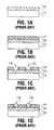
- FIGS. 1A through 1Dillustrate cross-sectional views of one example of a method for forming a BGA integrated circuit package in the prior art.
- a conductive wiring layer 110is applied to an entire integrated circuit wafer 112 .
- the integrated circuit wafer 112typically includes a plurality of individual integrated circuit devices, and the wiring layer 110 forms interconnections to the individual integrated circuit devices on the wafer 112 .
- a dielectric layer 114such as a layer of SiO 2 , is then formed over the wiring layer 110 .
- openings 116are then formed in the dielectric layer 114 for receiving solder balls. Typically, the openings 116 are formed over the integrated circuit devices.
- the integrated circuit wafer 112is then cut into individual packaged integrated circuit dies and solder balls 118 are deposited into the openings and reflowed to form the solder ball connections to the wiring layer 110 .
- the resulting integrated circuit packageshave a fan-in arrangement of the solder ball connections over the integrated circuit device.
- the integrated circuit packagesare then attached to other components, such as a printed circuit board having a heat sink that provides heat dissipation for the packaged integrated circuit device.
- FIG. 2illustrates a top view of one example of a fan-in pattern of a BGA packaged integrated circuit device in the prior art.
- the integrated circuit package 210has solder connections 212 located above the integrated circuit device 214 .
- the present inventionincludes methods for forming integrated circuit packages, such as BGA packaged integrated circuit packages, using fluidic self-assembly, and apparatuses formed thereby.
- functional componentssuch as electronic integrated circuit components, having a wired side are suspended in a fluid and flowed over a substrate.
- the substratehas a top layer of a first dielectric and has recessed receptor regions for receiving the functional components.
- the functional componentsare deposited in the receptor regions using fluidic self-assembly such that the wired side is facing outward from the receptor region.
- a conductive layer, such as a wiring layer,is then formed on the first dielectric forming conductive interconnects to the wired side of the functional component.
- a second dielectric layeris then fabricated on top of the conductive layer.
- the second dielectric layerhas openings for receiving conductive elements.
- Conductive elementssuch as solder balls, are deposited into the openings in the second dielectric layer and contact the conductive layer.
- the substratemay then be separated into individual integrated circuit packages.
- FIGS. 1A through 1Dillustrate cross-sectional views of one example of a method for forming a BGA integrated circuit package in the prior art.
- FIG. 2illustrates a top view of one example of a fan-in pattern of a BGA packaged integrated circuit device in the prior art.
- FIG. 3illustrates a general flow diagram of one embodiment of a method of forming an integrated circuit package using FSA according to one embodiment of the present invention.
- FIGS. 4A-4Oillustrate cross-sectional views of one embodiment of a method for forming integrated circuit device packages using fluidic self-assembly according to the present invention.
- FIG. 5shows a generalized top view of one embodiment of a 16 input/output integrated circuit package formed according to the present invention that illustrates the fan-out pattern of the conductive elements from the integrated circuit.
- FIG. 6illustrates alternate embodiments of planarization that may be used in forming integrated circuit packages according to the present invention.
- FIG. 7is a perspective view of an integrated circuit package according to the invention, including a package substrate and a semiconductor die.
- FIG. 8is a cross-sectional side view illustrating the components of FIG. 7 .
- FIG. 9is a view similar to FIG. 8 after the die is dropped in the opening in the substrate.
- the present inventionincludes methods for forming integrated circuit packages, such as BGA packaged devices, using fluidic self-assembly, and apparatuses formed thereby.
- ⁇ унк ⁇ ионал ⁇ н ⁇ е ⁇ оло ⁇ оловкиhaving a wired side are suspended in a fluid and flowed over a substrate.
- the substratehas a top first dielectric layer and has recessed receptor regions for receiving the functional components, such as integrated circuits.
- the functional componentsare deposited in the receptor regions using fluidic self-assembly such that the wired side of the functional component is facing outward from the receptor region.
- a conductive layersuch as a wiring layer, is then formed on the first dielectric layer.
- the conductive layeris formed such that conductive interconnects are formed to the functional components.
- a second dielectric layeris then fabricated on top of the conductive layer.
- the second dielectric layerhas openings for receiving conductive elements. Conductive elements, for example, solder balls, are deposited into the openings in the second dielectric layer and contact the conductive layer, e.g., the wiring layer.
- the substratemay then be separated into individual integrated circuit packages.
- FIG. 3illustrates a general flow diagram of one embodiment of a method of forming an integrated circuit package using FSA according to one embodiment of the present invention.
- a substrate material having a top first dielectric layeris obtained and receptor regions are formed in the substrate. This process is further described herein with reference to FIGS. 4A and 4B.
- the functional componentsare formed or obtained for assembly into the receptor regions of the substrate.
- the functional componentsmay be low-lead count integrated circuit devices such as op amps, 74XX series logic devices, etc., fabricated on self-assembling microstructures, such as shaped nanoblocks. The functional components are further described herein with reference to FIG. 4 C.
- the functional componentsare self-assembled into the receptor regions using fluidic self-assembly. This process is further described herein with reference to FIG. 4 C.
- the functional componentsare planarized into the substrate. This process is further described herein with reference to FIG. 4 D.
- interconnect viasare formed in the planarization layer. This process is further described herein with reference to FIGS. 4E and 4F.
- a conductive layersuch as a wiring layer, is formed. This process is further described herein with reference to FIG. 4 G.
- the conductive layeris patterned to form conductive interconnects, i.e., wiring, to the functional components. This process is further described herein with reference to FIGS. 4H through 4J.
- the conductive layeris electroplated to build up the connection. This process is further described herein with reference to FIG. 4 J.
- a second dielectric layeris formed. This process is further described herein with reference to FIG. 4 K.
- openingsare formed in the second dielectric layer outside the footprint of the functional component. This process is further described herein with reference to FIGS. 4L and 4M.
- conductive elementssuch as solder balls, are deposited in the openings, and reflowed to form electrical interconnections to the functional components. This process is further described herein with reference to FIGS. 4N and 4O.
- the integrated circuit packagesmay be removed from the substrate for use in other components or packaged for storage.
- the integrated circuit packagesmay be die cut, cut with a laser, or cut with a roll die.
- FIGS. 4A-4Oillustrate cross-sectional views of one embodiment of a method for forming integrated circuit device packages using fluidic self-assembly according to the present invention.
- the substrate 402may be a dual layer substrate formed of a top first dielectric layer 404 on a thermally conductive layer 406 .
- the top first dielectric layer 404may be silicon dioxide and the thermally conductive layer 406 may be aluminum.
- the first dielectric layer 404is about 50 microns thick and the thermally conductive layer 406 is about 50 microns thick. In other embodiments, the thickness of the first dielectric layer 404 and the thermally conductive layer 406 may be within a range between and including 25 to 100 microns each.
- top first dielectric layer 404may also be formed from other materials, such as polymers, i.e., polyethersulfone (PES), polysulfone (PS), etc.
- the thermally conductive layer 406may be formed of other metals or metal alloys, such as copper, copper-beryllium alloys, molybdenum, nickel, INVAR, INCONEL, etc.
- the substrate 402may also be formed of a single layer material, such as PES, PS, green ceramic tape, etc., or may be multi-layered to accommodate different technical parameters of the integrated circuit package, such as voltage, flexibility, temperature, etc.
- the substrate 402is recessed to form receptor regions 408 into which functional components will assemble through fluidic self-assembly (FSA).
- FSAfluidic self-assembly
- the receptor regions 408may be spaced and arranged in a variety of patterns to accommodate a desired integrated circuit package design.
- the receptor regions 408may be formed through the first dielectric layer 404 using a hot stamp process so that the thermally conductive layer 406 is exposed at the bottom of the receptor region 408 .
- the receptor regions 408may be formed using a template punch, or laser, chemical or plasma etching, a cast, or impact extrusion.
- U.S. Pat. No. 5,545,291describes formation of recessed regions in a substrate for use in FSA and is incorporated herein by reference.
- the receptor regions 408are formed so that the functional components assemble into the receptor regions 408 in a top up/bottom down orientation, i.e., the receptor regions 408 may be keyed.
- the receptor regions 408may be formed as trapezoidal shaped recesses.
- a slurry containing a plurality of functional devicesis flowed over the recessed substrate.
- the functional devicesfall into the recesses in the substrate.
- the excess slurryis collected and recycled.
- the substrateis checked for empty recessed regions. For example, an electronic eye may view the substrate for empty regions. Functional devices may then be robotically placed into the empty regions.
- the functional components 410may be low lead count devices, such as op-amps or 74XX series logic devices, however, it will be appreciated that other devices may also be utilized.
- the functional components 410may be fabricated as trapezoidal-shaped nanoblocks that are narrower at the base end than at the top, where the wired side, e.g., the side having circuit leads, of the functional component resides at the top of the nanoblock.
- the blocksmay for example be frustum-conical or frustum-pyramydal.
- the receptor regions 408may also be trapezoidally shaped to receive the nanoblock in a top/bottom orientation so that the top wired side of the functional component 410 faces outward from the receptor region 408 .
- Formation of the functional component 410 such that the circuitry, e.g., the wired side, is at the top of the nanoblockallows for interconnections to be formed to the circuit leads. Also, this top/bottom orientation allows the bottom of the nanoblock to contact the exposed thermally conductive layer 406 . This contact provides for heat dissipation from the functional component 410 to the thermally conductive layer 406 . In this way, a separate heat sink for the integrated circuit package is not necessary as it is an intrinsic part of the substrate 402 . This provides greater flexibility in designing pad limited components as heat dissipation is accomplished by the integrated circuit package, e.g., circuit board space previously needed for heat sinks may be utilized for other purposes. It will be appreciated that even in a single layer substrate 402 , the choice of substrate material, may also provide heat dissipation, for example, ceramic substrates.
- the functional components 410 and/or receptor regions 408may be designed differently, for example, keyed, so that the functional components 410 orient in the receptor regions 408 in one or more predetermined orientations.
- the trapezoidal shaped nanoblock and receptor regionmay be further shaped with one set of parallel sides longer than the other set of parallel sides to limit left/right orientations.
- the shaped nanoblockmay be further shaped so that it may only orient in one way in the receptor region, e.g., all sides are different. It will be appreciated that the functional components 410 and/or receptor regions 408 may be differently keyed to achieve the same or different effects.
- the functional components 410are planarized into the substrate.
- the planarizationmay be accomplished by coating the surface of the substrate 402 including the assembled functional components 410 with a planarization layer 412 , such as a photo polymer or a photoresist that is spun to flatten or lapped to flatten.
- the planarization layer 412is patterned for the formation of interconnect vias and exposed to establish a circuit pattern.
- the photo polymermay be a negative photoresist, such as epoxy methyacrelate.
- the photoresistis then exposed.
- the exposure of the negative photoresistmay be performed centered on the I-line.
- the exposed photoresistis developed, and the remaining photoresist is cured.
- the photoresistmay be cured in a batch oven at 150° C. for approximately one hour.
- the patternis developed to form the interconnect vias 414 . It will be appreciated that other methods for the planarization and formation of the interconnect vias may also be utilized.
- other embodiments of the present inventionmay utilize planarization methods described further herein with reference to FIG. 6 .
- a conductive layer 416is formed.
- the conductive layer 416may be a wiring layer, such as an aluminum layer formed by vapor deposition, for example, by sputtering aluminum. It will be appreciated that other conductive materials may also be used, for example, conductive polymers, metals (e.g., copper, silver, gold, chromium, etc.), metal alloys, metal particles, conductive organic compounds, or conductive oxides.
- the conductive layer 416may be formed by vapor deposition of more than one metal, for example, a deposition of 100 angstroms chromium and 1500 ⁇ copper in a single pass machine. In other embodiments, the vapor deposition may be accomplished in a multi-pass machine.
- the conductive layer 416is coated with a photoresist layer, patterned, exposed and developed for the formation of protective layers over the interconnect vias 414 .
- the exposed conductive layer 416is etched forming conductive interconnects 417 , e.g., wiring, to the functional component 410 .
- the protective layeris removed leaving the conductive interconnects 417 . It should be noted that the conductive interconnects 417 extend outside the footprint of the functional component 410 .
- the interconnects 417may be further built up by electroplating another layer of conductive material onto the interconnects 417 .
- the interconnects 417may be further built up by electroplating on a copper layer have a thickness in the range between and including 10-15 microns. It will be appreciated that other conductive materials may be used in electroplating up the interconnects 417 .
- a second dielectric layer 420 such as SiO 2is formed 417 , i.e., above the interconnects 417 and exposed top of the substrate 402 .
- the second dielectric layer 420is then patterned and exposed for the formation of openings.
- the patternis developed to form openings 422 for receiving conductive elements.
- conductive elements 424are deposited into the openings 422 .
- the conductive elements 424may be solder balls deposited by a pick and place method. It will be appreciated that other conductive elements may also be utilized, such as gold puffs, springs, etc.
- the conductive elements 424may be reflowed establishing a conductive interconnection through the conductive interconnects 417 to the functional components 410 .
- the integrated circuit packagesmay then be singulated, i.e., for example, cut and excised from the main body of the substrate.
- FIG. 5shows a generalized top view of one embodiment of a 16 input/output integrated circuit package formed according to the present invention that illustrates the fan-out pattern of the conductive elements from the integrated circuit.
- the resultant integrated circuit packagehas a fan-out pattern rather than a fan-in pattern as seen in the prior art example illustrated at FIG. 2 .
- the conductive elements 524for example, the solder balls, are peripheral to the functional component 510 .
- This fan-out designallows for some design independence from the ever-decreasing size of the integrated circuit component.
- the integrated circuitmay decrease in size and have finer interconnection patterns independent of the size of the conductive elements as the conductive elements reside outside the integrated circuit.
- FIG. 6illustrates alternate embodiments of planarization that may be used in forming integrated circuit packages according to the present invention.
- the substrate with assembled functional componentsmay be coated with a non-photo polymer.
- the polymeris cured.
- the polymermay be coated with a photoresist.
- the photoresistis exposed.
- the photo resistis developed, etched and stripped forming the interconnect vias in preparation for formation of the conductive interconnects.
- the polymermay be laser ablated.
- the surfacemay be wet cleaned.
- the surfacemay then be plasma cleaned stripped forming the interconnect vias in preparation for formation of the conductive interconnects.
- FIGS. 7, 8 and 9now illustrate an integrated circuit package 710 which is manufactured according to the method hereinbefore described.
- the semifconductor package 710includes a package substrate 712 and an integrated circuit die 714 .
- the substrate 712includes two layers, the first being an alumidnum metal layer 716 and the second being a dielectric layer 718 which is formed on the alumidnum layer 716 .
- the aluminum layer 716forms a lower surface 720 of the substrate 712 .
- the dielectric layer 718is formed directly on the aluminum layer 716 .
- An upper surface 726 of the dielectric layer 718forms an upper surface of the substrate 712 .
- An opening 728is formed in the dielectric layer 726 .
- the opening 728has a periphery 730 in the upper surface 726 .
- the periphery 730has four straight edges 732 .
- the shape of the periphery 730may be different.
- the periphery 730has a width 734 and a length 736 .
- a lower surface 738 of the opening 728is formed by the metal layer 716 .
- the metal layer 716is continuous from the lower surface 738 of the opening 728 to the lower surface 720 of the substrate 712 .
- a metal layermay be deposited in the opening 728 .
- the opening 728has four sides 742 .
- Each side 742extends from a respective edge 732 to a respective edge 744 of a periphery of the lower surface 738 .
- the respective side 742extends from the respective edge 732 towards the respective edge 744 downwardly and away from the edge 732 .
- opposing sides 742extend downwardly and towards one another. Extensions of opposing sides 742 will meet at a point below the lower surface 738 .
- the opening 728has an inverted frustum-pyramydal shape having a square base. In another embodiment the shape of the opening 728 may be different.
- the die 714includes a semiconductor substrate 750 , typically made of silicon, and an integrated circuit 752 formed on an upper surface of the substrate 750 .
- a lower surface 754 of the substrate 750forms a lower surface of the die 714 .
- the integrated circuit 752is formed at or near an upper surface 757 of the die 714 .
- a plurality of bond pads 757are formed on the upper surface 756 . Each bond pad 757 is connected to the integrated circuit 752 . Electronic signals can be transferred through the bond pad 757 to and from the integrated circuit 752 .
- the surface 756is substantially flat and has a periphery 758 .
- the periphery 758had a width 760 and a length 762 .
- the width 760is substantially the same as the width 734 and substantially more than the width 722 .
- the length 762is substantially the same as the length 736 and substantially more than the length 724 .
- the periphery 758is substantially square and has a shape which is complementary to the shape of the periphery 730 .
- the die 714has four sides 764 .
- Each side 764extends from a respective edge 766 to respective edge 768 of a periphery of the lower surface 754 .
- a respective side 764extends at an angle with respect to vertical so that the side 764 extends from the periphery 766 downwardly and under the surface 756 towards the edge 768 .
- Opposing ones of the sides 768thus extend downwardly and towards one another. Extensions of the sides 764 will meet at a point below the surface 754 .
- the die 714has an inverted frustum-pyramydal shape with a square base.
- the shape of the opening 728is in all respects substantially complementary to the shape of the die 714 .
- the lower surface 754is located against the lower surface 738 and the sides 764 contact the sides 742 .
- the upper surface 756is then substantially flush with the upper surface 726 .
- the semiconductor packageis thereafter finally manufactured as shown in FIG. 4 N.
Landscapes
- Engineering & Computer Science (AREA)
- Computer Hardware Design (AREA)
- Microelectronics & Electronic Packaging (AREA)
- Power Engineering (AREA)
- Physics & Mathematics (AREA)
- Condensed Matter Physics & Semiconductors (AREA)
- General Physics & Mathematics (AREA)
- Manufacturing & Machinery (AREA)
- Chemical & Material Sciences (AREA)
- Materials Engineering (AREA)
- Cooling Or The Like Of Semiconductors Or Solid State Devices (AREA)
Abstract
Description
Claims (12)
Priority Applications (2)
| Application Number | Priority Date | Filing Date | Title |
|---|---|---|---|
| US09/825,381US6417025B1 (en) | 2001-04-02 | 2001-04-02 | Integrated circuit packages assembled utilizing fluidic self-assembly |
| US10/177,045US6566744B2 (en) | 2001-04-02 | 2002-06-21 | Integrated circuit packages assembled utilizing fluidic self-assembly |
Applications Claiming Priority (1)
| Application Number | Priority Date | Filing Date | Title |
|---|---|---|---|
| US09/825,381US6417025B1 (en) | 2001-04-02 | 2001-04-02 | Integrated circuit packages assembled utilizing fluidic self-assembly |
Related Child Applications (1)
| Application Number | Title | Priority Date | Filing Date |
|---|---|---|---|
| US10/177,045DivisionUS6566744B2 (en) | 2001-04-02 | 2002-06-21 | Integrated circuit packages assembled utilizing fluidic self-assembly |
Publications (1)
| Publication Number | Publication Date |
|---|---|
| US6417025B1true US6417025B1 (en) | 2002-07-09 |
Family
ID=25243874
Family Applications (2)
| Application Number | Title | Priority Date | Filing Date |
|---|---|---|---|
| US09/825,381Expired - LifetimeUS6417025B1 (en) | 2001-04-02 | 2001-04-02 | Integrated circuit packages assembled utilizing fluidic self-assembly |
| US10/177,045Expired - LifetimeUS6566744B2 (en) | 2001-04-02 | 2002-06-21 | Integrated circuit packages assembled utilizing fluidic self-assembly |
Family Applications After (1)
| Application Number | Title | Priority Date | Filing Date |
|---|---|---|---|
| US10/177,045Expired - LifetimeUS6566744B2 (en) | 2001-04-02 | 2002-06-21 | Integrated circuit packages assembled utilizing fluidic self-assembly |
Country Status (1)
| Country | Link |
|---|---|
| US (2) | US6417025B1 (en) |
Cited By (122)
| Publication number | Priority date | Publication date | Assignee | Title |
|---|---|---|---|---|
| US20020088267A1 (en)* | 2000-10-27 | 2002-07-11 | Harald Beck | Method and device for controlling a setting element in a vehicle |
| US20020158577A1 (en)* | 2000-07-07 | 2002-10-31 | Tatsuya Shimoda | Organic electroluminescent display and manufacturing method thereof, electro-optic device and manufacturing method thereof, and electronic device |
| US20030062123A1 (en)* | 2001-09-28 | 2003-04-03 | Hrl Laboratories, Llc | Method of self-latching for adhesion during self-assembly of electronic or optical components |
| US20030068519A1 (en)* | 2001-09-28 | 2003-04-10 | Hrl Laboratories, Llc | Method for assembly of complementary-shaped receptacle site and device microstructures |
| US20030112576A1 (en)* | 2001-09-28 | 2003-06-19 | Brewer Peter D. | Process for producing high performance interconnects |
| US20040026754A1 (en)* | 2002-08-07 | 2004-02-12 | Peikang Liu | Radio frequency identification device and method |
| US6693384B1 (en)* | 2002-02-01 | 2004-02-17 | Alien Technology Corporation | Interconnect structure for electronic devices |
| US20040142575A1 (en)* | 2002-07-25 | 2004-07-22 | Brewer Peter D. | Large area printing method for integrating device and circuit components |
| US20040160233A1 (en)* | 2003-02-13 | 2004-08-19 | Forster Ian J. | RFID device tester and method |
| US20040183182A1 (en)* | 2002-01-23 | 2004-09-23 | Susan Swindlehurst | Apparatus incorporating small-feature-size and large-feature-size components and method for making same |
| US20040195319A1 (en)* | 2003-04-03 | 2004-10-07 | Forster Ian J. | RFID device detection system and method |
| US20040200061A1 (en)* | 2003-04-11 | 2004-10-14 | Coleman James P. | Conductive pattern and method of making |
| US6863219B1 (en)* | 2001-08-17 | 2005-03-08 | Alien Technology Corporation | Apparatuses and methods for forming electronic assemblies |
| US20050124093A1 (en)* | 2003-12-03 | 2005-06-09 | Wen-Kun Yang | Fan out type wafer level package structure and method of the same |
| US20050238967A1 (en)* | 2004-04-27 | 2005-10-27 | The Board Of Trustees Of The University Of Illinois | Composite patterning devices for soft lithography |
| US20050253273A1 (en)* | 2003-11-05 | 2005-11-17 | California Institute Of Technology | Method for integrating pre-fabricated chip structures into functional electronic systems |
| US20060000907A1 (en)* | 2004-07-01 | 2006-01-05 | Forster Ian J | RFID device preparation system and method |
| US20060051517A1 (en)* | 2004-09-03 | 2006-03-09 | Eastman Kodak Company | Thermally controlled fluidic self-assembly method and support |
| US20060055542A1 (en)* | 2004-09-13 | 2006-03-16 | Forster Ian J | RFID device with content insensitivity and position insensitivity |
| US20060054710A1 (en)* | 2003-04-10 | 2006-03-16 | Forster Ian J | RFID devices having self-compensating antennas and conductive shields |
| US20060057293A1 (en)* | 2004-09-03 | 2006-03-16 | Eastman Kodak Company | Thermally controlled fluidic self-assembly |
| US20060091225A1 (en)* | 2003-11-04 | 2006-05-04 | Forster Ian J | RFID tag using a surface insensitive antenna structure |
| US20060148166A1 (en)* | 2004-11-08 | 2006-07-06 | Craig Gordon S | Assembly comprising functional devices and method of making same |
| US20060231958A1 (en)* | 2003-12-03 | 2006-10-19 | Advanced Chip Engineering Technology, Inc. | Fan out type wafer level package structure and method of the same |
| US20060246619A1 (en)* | 2002-05-29 | 2006-11-02 | Seiko Epson Corporation | Electro-optical device and method of manufacturing the same, element driving device and method of manufacturing the same, element substrate, and electronic apparatus |
| US20060286785A1 (en)* | 2004-06-04 | 2006-12-21 | The Board Of Trustees Of The University Of Illinois | A Stretchable Form of Single Crystal Silicon for High Performance Electronics on Rubber Substrates |
| US7154283B1 (en) | 2006-02-22 | 2006-12-26 | Avery Dennison Corporation | Method of determining performance of RFID devices |
| US20070032089A1 (en)* | 2004-06-04 | 2007-02-08 | The Board Of Trustees Of The University Of Illinois | Printable Semiconductor Structures and Related Methods of Making and Assembling |
| US20070031992A1 (en)* | 2005-08-05 | 2007-02-08 | Schatz Kenneth D | Apparatuses and methods facilitating functional block deposition |
| US20070031759A1 (en)* | 2005-04-21 | 2007-02-08 | Webster Dean C | Radiation curable polymer films having improved laser ablation properties and radiation curable sensitizers therefor |
| US20070039687A1 (en)* | 2005-08-22 | 2007-02-22 | Hamilton Kevin S | Method of making RFID devices |
| US7218527B1 (en)* | 2001-08-17 | 2007-05-15 | Alien Technology Corporation | Apparatuses and methods for forming smart labels |
| US7223635B1 (en) | 2003-07-25 | 2007-05-29 | Hrl Laboratories, Llc | Oriented self-location of microstructures with alignment structures |
| US20070158804A1 (en)* | 2006-01-10 | 2007-07-12 | Semiconductor Energy Laboratory Co., Ltd. | Semiconductor device, manufacturing method of semiconductor device, and RFID tag |
| US7251882B2 (en) | 2004-09-03 | 2007-08-07 | Eastman Kodak Company | Method for assembling micro-components to binding sites |
| US7253735B2 (en) | 2003-03-24 | 2007-08-07 | Alien Technology Corporation | RFID tags and processes for producing RFID tags |
| US7260882B2 (en) | 2001-05-31 | 2007-08-28 | Alien Technology Corporation | Methods for making electronic devices with small functional elements supported on a carriers |
| US7288432B2 (en) | 1999-03-16 | 2007-10-30 | Alien Technology Corporation | Electronic devices with small functional elements supported on a carrier |
| US20080055581A1 (en)* | 2004-04-27 | 2008-03-06 | Rogers John A | Devices and methods for pattern generation by ink lithography |
| US7385284B2 (en) | 2004-11-22 | 2008-06-10 | Alien Technology Corporation | Transponder incorporated into an electronic device |
| US20080157235A1 (en)* | 2004-06-04 | 2008-07-03 | Rogers John A | Controlled buckling structures in semiconductor interconnects and nanomembranes for stretchable electronics |
| US20080170982A1 (en)* | 2004-11-09 | 2008-07-17 | Board Of Regents, The University Of Texas System | Fabrication and Application of Nanofiber Ribbons and Sheets and Twisted and Non-Twisted Nanofiber Yarns |
| US7452748B1 (en) | 2004-11-08 | 2008-11-18 | Alien Technology Corporation | Strap assembly comprising functional block deposited therein and method of making same |
| US20080293175A1 (en)* | 2006-03-10 | 2008-11-27 | Matsushita Electric Industrial Co., Ltd. | Method for mounting anisotropically-shaped members |
| US20080297453A1 (en)* | 2007-05-31 | 2008-12-04 | Applied Printed Electronics Holdings, Inc. | Method of Manufacturing Addressable and Static Electronic Displays |
| US7542301B1 (en) | 2005-06-22 | 2009-06-02 | Alien Technology Corporation | Creating recessed regions in a substrate and assemblies having such recessed regions |
| US7551141B1 (en) | 2004-11-08 | 2009-06-23 | Alien Technology Corporation | RFID strap capacitively coupled and method of making same |
| US7557367B2 (en) | 2004-06-04 | 2009-07-07 | The Board Of Trustees Of The University Of Illinois | Stretchable semiconductor elements and stretchable electrical circuits |
| US20090184417A1 (en)* | 2006-04-21 | 2009-07-23 | Webster Dean C | Polyol photosensitizers, carrier gas uv laser ablation sensitizers, and other additives and methods for making and using same |
| US20090265929A1 (en)* | 2005-09-29 | 2009-10-29 | Matsushita Electric Industrial Co., Ltd. | Method of mounting electronic circuit constituting member and relevant mounting apparatus |
| US20100052112A1 (en)* | 2008-04-03 | 2010-03-04 | Rogers John A | Printable, Flexible and Stretchable Diamond for Thermal Management |
| US20100065862A1 (en)* | 2007-05-31 | 2010-03-18 | Nthdegree Technologies Worldwide Inc. | Light Emitting, Photovoltaic Or Other Electronic Apparatus and System |
| US7688206B2 (en) | 2004-11-22 | 2010-03-30 | Alien Technology Corporation | Radio frequency identification (RFID) tag for an item having a conductive layer included or attached |
| US7687277B2 (en) | 2004-12-22 | 2010-03-30 | Eastman Kodak Company | Thermally controlled fluidic self-assembly |
| US20100167441A1 (en)* | 2007-05-31 | 2010-07-01 | Nthdegree Technologies Worldwide Inc. | Method of Manufacturing a Light Emitting, Photovoltaic or Other Electronic Apparatus and System |
| US20100187002A1 (en)* | 2009-01-29 | 2010-07-29 | Seung Seoup Lee | Method of attaching die using self-assembling monolayer and package substrate including die attached thereto using self-assembling monolayer |
| US7814648B2 (en) | 2008-11-26 | 2010-10-19 | Panasonic Corporation | Method of disposing an electronic device on an electrode formed on substrate |
| US20100266769A1 (en)* | 2008-11-18 | 2010-10-21 | Panasonic Corporation | Component mounting method |
| US20100283615A1 (en)* | 2003-04-11 | 2010-11-11 | Avery Dennison Corporation | Conductive Pattern and Method of Making |
| US20100283069A1 (en)* | 2007-01-17 | 2010-11-11 | John Rogers | Optical systems fabricated by printing-based assembly |
| US20100308719A1 (en)* | 2004-12-27 | 2010-12-09 | Nthdegree Technologies Worldwide Inc. | Static and Addressable Emissive Displays |
| US20110034912A1 (en)* | 2008-10-07 | 2011-02-10 | Mc10, Inc. | Systems,methods, and devices having stretchable integrated circuitry for sensing and delivering therapy |
| US7943491B2 (en) | 2004-06-04 | 2011-05-17 | The Board Of Trustees Of The University Of Illinois | Pattern transfer printing by kinetic control of adhesion to an elastomeric stamp |
| US20110123794A1 (en)* | 2008-07-25 | 2011-05-26 | Cornell University | Apparatus and methods for digital manufacturing |
| US20110147715A1 (en)* | 2008-06-16 | 2011-06-23 | Purdue Research Foundation | Medium Scale Carbon Nanotube Thin Film Integrated Circuits on Flexible Plastic Substrates |
| US8349653B2 (en) | 2010-06-02 | 2013-01-08 | Maxim Integrated Products, Inc. | Use of device assembly for a generalization of three-dimensional metal interconnect technologies |
| US8367035B2 (en) | 2006-03-03 | 2013-02-05 | The Board Of Trustees Of The University Of Illinois | Methods of making spatially aligned nanotubes and nanotube arrays |
| US8372726B2 (en) | 2008-10-07 | 2013-02-12 | Mc10, Inc. | Methods and applications of non-planar imaging arrays |
| US8389862B2 (en) | 2008-10-07 | 2013-03-05 | Mc10, Inc. | Extremely stretchable electronics |
| US8413359B2 (en) | 2008-05-13 | 2013-04-09 | Nthdegree Technologies Worldwide Inc | Illuminating display systems |
| US8415879B2 (en) | 2007-05-31 | 2013-04-09 | Nthdegree Technologies Worldwide Inc | Diode for a printable composition |
| JP2013106033A (en)* | 2011-11-10 | 2013-05-30 | Samsung Electro-Mechanics Co Ltd | Semiconductor package and method of manufacturing the same |
| US8552299B2 (en) | 2008-03-05 | 2013-10-08 | The Board Of Trustees Of The University Of Illinois | Stretchable and foldable electronic devices |
| US8666471B2 (en) | 2010-03-17 | 2014-03-04 | The Board Of Trustees Of The University Of Illinois | Implantable biomedical devices on bioresorbable substrates |
| US8674593B2 (en) | 2007-05-31 | 2014-03-18 | Nthdegree Technologies Worldwide Inc | Diode for a printable composition |
| US8739441B2 (en) | 2008-05-13 | 2014-06-03 | Nthdegree Technologies Worldwide Inc | Apparatuses for providing power for illumination of a display object |
| US8809126B2 (en) | 2007-05-31 | 2014-08-19 | Nthdegree Technologies Worldwide Inc | Printable composition of a liquid or gel suspension of diodes |
| US8846457B2 (en) | 2007-05-31 | 2014-09-30 | Nthdegree Technologies Worldwide Inc | Printable composition of a liquid or gel suspension of diodes |
| US8852467B2 (en) | 2007-05-31 | 2014-10-07 | Nthdegree Technologies Worldwide Inc | Method of manufacturing a printable composition of a liquid or gel suspension of diodes |
| US8865489B2 (en) | 2009-05-12 | 2014-10-21 | The Board Of Trustees Of The University Of Illinois | Printed assemblies of ultrathin, microscale inorganic light emitting diodes for deformable and semitransparent displays |
| US8877101B2 (en) | 2007-05-31 | 2014-11-04 | Nthdegree Technologies Worldwide Inc | Method of manufacturing a light emitting, power generating or other electronic apparatus |
| US8886334B2 (en) | 2008-10-07 | 2014-11-11 | Mc10, Inc. | Systems, methods, and devices using stretchable or flexible electronics for medical applications |
| US8934965B2 (en) | 2011-06-03 | 2015-01-13 | The Board Of Trustees Of The University Of Illinois | Conformable actively multiplexed high-density surface electrode array for brain interfacing |
| US9018833B2 (en) | 2007-05-31 | 2015-04-28 | Nthdegree Technologies Worldwide Inc | Apparatus with light emitting or absorbing diodes |
| US9159635B2 (en) | 2011-05-27 | 2015-10-13 | Mc10, Inc. | Flexible electronic structure |
| US9171794B2 (en) | 2012-10-09 | 2015-10-27 | Mc10, Inc. | Embedding thin chips in polymer |
| US9289132B2 (en) | 2008-10-07 | 2016-03-22 | Mc10, Inc. | Catheter balloon having stretchable integrated circuitry and sensor array |
| US9343593B2 (en) | 2007-05-31 | 2016-05-17 | Nthdegree Technologies Worldwide Inc | Printable composition of a liquid or gel suspension of diodes |
| US9419179B2 (en) | 2007-05-31 | 2016-08-16 | Nthdegree Technologies Worldwide Inc | Diode for a printable composition |
| US9425357B2 (en) | 2007-05-31 | 2016-08-23 | Nthdegree Technologies Worldwide Inc. | Diode for a printable composition |
| US9442285B2 (en) | 2011-01-14 | 2016-09-13 | The Board Of Trustees Of The University Of Illinois | Optical component array having adjustable curvature |
| US9534772B2 (en) | 2007-05-31 | 2017-01-03 | Nthdegree Technologies Worldwide Inc | Apparatus with light emitting diodes |
| US9554484B2 (en) | 2012-03-30 | 2017-01-24 | The Board Of Trustees Of The University Of Illinois | Appendage mountable electronic devices conformable to surfaces |
| US9691873B2 (en) | 2011-12-01 | 2017-06-27 | The Board Of Trustees Of The University Of Illinois | Transient devices designed to undergo programmable transformations |
| US9723122B2 (en) | 2009-10-01 | 2017-08-01 | Mc10, Inc. | Protective cases with integrated electronics |
| US9722145B2 (en) | 2015-06-24 | 2017-08-01 | Sharp Laboratories Of America, Inc. | Light emitting device and fluidic manufacture thereof |
| US9765934B2 (en) | 2011-05-16 | 2017-09-19 | The Board Of Trustees Of The University Of Illinois | Thermally managed LED arrays assembled by printing |
| US9825202B2 (en) | 2014-10-31 | 2017-11-21 | eLux, Inc. | Display with surface mount emissive elements |
| US9936574B2 (en) | 2009-12-16 | 2018-04-03 | The Board Of Trustees Of The University Of Illinois | Waterproof stretchable optoelectronics |
| US10236279B2 (en) | 2014-10-31 | 2019-03-19 | eLux, Inc. | Emissive display with light management system |
| US10242977B2 (en) | 2014-10-31 | 2019-03-26 | eLux, Inc. | Fluid-suspended microcomponent harvest, distribution, and reclamation |
| US10312731B2 (en) | 2014-04-24 | 2019-06-04 | Westrock Shared Services, Llc | Powered shelf system for inductively powering electrical components of consumer product packages |
| US10319878B2 (en) | 2014-10-31 | 2019-06-11 | eLux, Inc. | Stratified quantum dot phosphor structure |
| US10381332B2 (en) | 2014-10-31 | 2019-08-13 | eLux Inc. | Fabrication method for emissive display with light management system |
| US10381335B2 (en) | 2014-10-31 | 2019-08-13 | ehux, Inc. | Hybrid display using inorganic micro light emitting diodes (uLEDs) and organic LEDs (OLEDs) |
| US10418527B2 (en) | 2014-10-31 | 2019-09-17 | eLux, Inc. | System and method for the fluidic assembly of emissive displays |
| US10446728B2 (en) | 2014-10-31 | 2019-10-15 | eLux, Inc. | Pick-and remove system and method for emissive display repair |
| US10441185B2 (en) | 2009-12-16 | 2019-10-15 | The Board Of Trustees Of The University Of Illinois | Flexible and stretchable electronic systems for epidermal electronics |
| US10516084B2 (en) | 2014-10-31 | 2019-12-24 | eLux, Inc. | Encapsulated fluid assembly emissive elements |
| US10520769B2 (en) | 2014-10-31 | 2019-12-31 | eLux, Inc. | Emissive display with printed light modification structures |
| US10535640B2 (en) | 2014-10-31 | 2020-01-14 | eLux Inc. | System and method for the fluidic assembly of micro-LEDs utilizing negative pressure |
| US10543486B2 (en) | 2014-10-31 | 2020-01-28 | eLux Inc. | Microperturbation assembly system and method |
| US10672748B1 (en) | 2010-06-02 | 2020-06-02 | Maxim Integrated Products, Inc. | Use of device assembly for a generalization of three-dimensional heterogeneous technologies integration |
| DE102018009472A1 (en) | 2018-12-03 | 2020-06-04 | Giesecke+Devrient Currency Technology Gmbh | Application and attachment of a certain number of individual elements on a substrate web |
| DE102018009475A1 (en) | 2018-12-03 | 2020-06-04 | Giesecke+Devrient Currency Technology Gmbh | Application and fastening of individual elements on a substrate web |
| US10918298B2 (en) | 2009-12-16 | 2021-02-16 | The Board Of Trustees Of The University Of Illinois | High-speed, high-resolution electrophysiology in-vivo using conformal electronics |
| US10925543B2 (en) | 2015-11-11 | 2021-02-23 | The Board Of Trustees Of The University Of Illinois | Bioresorbable silicon electronics for transient implants |
| US11029198B2 (en) | 2015-06-01 | 2021-06-08 | The Board Of Trustees Of The University Of Illinois | Alternative approach for UV sensing |
| US11118965B2 (en) | 2015-06-01 | 2021-09-14 | The Board Of Trustees Of The University Of Illinois | Miniaturized electronic systems with wireless power and near-field communication capabilities |
| US11562984B1 (en) | 2020-10-14 | 2023-01-24 | Hrl Laboratories, Llc | Integrated mechanical aids for high accuracy alignable-electrical contacts |
| US12057429B1 (en) | 2021-06-23 | 2024-08-06 | Hrl Laboratories, Llc | Temporary bonding structures for die-to-die and wafer-to-wafer bonding |
| US12444712B1 (en) | 2022-12-06 | 2025-10-14 | Hrl Laboratories, Llc | Integrated mechanical aids for high accuracy alignable-electrical contacts |
Families Citing this family (35)
| Publication number | Priority date | Publication date | Assignee | Title |
|---|---|---|---|---|
| KR100481216B1 (en)* | 2002-06-07 | 2005-04-08 | 엘지전자 주식회사 | Ball Grid Array Package And Method Of Fabricating The Same |
| US7990349B2 (en)* | 2005-04-22 | 2011-08-02 | The Invention Science Fund I, Llc | Superimposed displays |
| US8711063B2 (en) | 2005-03-11 | 2014-04-29 | The Invention Science Fund I, Llc | Self assembly of elements for displays |
| US8334819B2 (en)* | 2005-03-11 | 2012-12-18 | The Invention Science Fund I, Llc | Superimposed displays |
| US7662008B2 (en)* | 2005-04-04 | 2010-02-16 | Searete Llc | Method of assembling displays on substrates |
| US20060202944A1 (en)* | 2005-03-11 | 2006-09-14 | Searete Llc, A Limited Liability Corporation Of The State Of Delaware | Elements for self assembling displays |
| US7977130B2 (en)* | 2006-08-03 | 2011-07-12 | The Invention Science Fund I, Llc | Method of assembling displays on substrates |
| US8390537B2 (en)* | 2005-03-11 | 2013-03-05 | The Invention Science Fund I, Llc | Method of assembling displays on substrates |
| US8300007B2 (en)* | 2005-03-11 | 2012-10-30 | The Invention Science Fund I, Llc | Self assembling display with substrate |
| US9153163B2 (en)* | 2005-03-11 | 2015-10-06 | The Invention Science Fund I, Llc | Self assembly of elements for displays |
| US8860635B2 (en)* | 2005-04-04 | 2014-10-14 | The Invention Science Fund I, Llc | Self assembling display with substrate |
| US7364983B2 (en)* | 2005-05-04 | 2008-04-29 | Avery Dennison Corporation | Method and apparatus for creating RFID devices |
| WO2006125206A2 (en)* | 2005-05-19 | 2006-11-23 | Avery Dennison Corporation | Method and apparatus for rfid device assembly |
| US20060280912A1 (en)* | 2005-06-13 | 2006-12-14 | Rong-Chang Liang | Non-random array anisotropic conductive film (ACF) and manufacturing processes |
| US8802214B2 (en) | 2005-06-13 | 2014-08-12 | Trillion Science, Inc. | Non-random array anisotropic conductive film (ACF) and manufacturing processes |
| KR100723493B1 (en)* | 2005-07-18 | 2007-06-04 | 삼성전자주식회사 | Smart card module substrate capable of wire bonding and flip chip bonding and smart card module including the same |
| US7662708B2 (en)* | 2005-07-27 | 2010-02-16 | Palo Alto Research Center Incorporated | Self-assembled interconnection particles |
| US7504331B2 (en)* | 2005-07-27 | 2009-03-17 | Palo Alto Research Center Incorporated | Method of fabricating self-assembled electrical interconnections |
| US7525194B2 (en)* | 2005-07-27 | 2009-04-28 | Palo Alto Research Center Incorporated | System including self-assembled interconnections |
| US20070146135A1 (en)* | 2005-12-27 | 2007-06-28 | David Boyadjieff | Assembling RFID components using webs |
| US20080122119A1 (en)* | 2006-08-31 | 2008-05-29 | Avery Dennison Corporation | Method and apparatus for creating rfid devices using masking techniques |
| US7923488B2 (en)* | 2006-10-16 | 2011-04-12 | Trillion Science, Inc. | Epoxy compositions |
| US7560303B2 (en)* | 2006-11-07 | 2009-07-14 | Avery Dennison Corporation | Method and apparatus for linear die transfer |
| KR100914892B1 (en)* | 2008-04-03 | 2009-08-31 | 삼성전기주식회사 | Ball grid array package and manufacturing method thereof |
| US9475963B2 (en) | 2011-09-15 | 2016-10-25 | Trillion Science, Inc. | Fixed array ACFs with multi-tier partially embedded particle morphology and their manufacturing processes |
| US9102851B2 (en) | 2011-09-15 | 2015-08-11 | Trillion Science, Inc. | Microcavity carrier belt and method of manufacture |
| US9352539B2 (en) | 2013-03-12 | 2016-05-31 | Trillion Science, Inc. | Microcavity carrier with image enhancement for laser ablation |
| US9917226B1 (en) | 2016-09-15 | 2018-03-13 | Sharp Kabushiki Kaisha | Substrate features for enhanced fluidic assembly of electronic devices |
| US10249599B2 (en) | 2016-06-29 | 2019-04-02 | eLux, Inc. | Laminated printed color conversion phosphor sheets |
| US9755110B1 (en) | 2016-07-27 | 2017-09-05 | Sharp Laboratories Of America, Inc. | Substrate with topological features for steering fluidic assembly LED disks |
| US9892944B2 (en) | 2016-06-23 | 2018-02-13 | Sharp Kabushiki Kaisha | Diodes offering asymmetric stability during fluidic assembly |
| US9985190B2 (en) | 2016-05-18 | 2018-05-29 | eLux Inc. | Formation and structure of post enhanced diodes for orientation control |
| US9627437B1 (en) | 2016-06-30 | 2017-04-18 | Sharp Laboratories Of America, Inc. | Patterned phosphors in through hole via (THV) glass |
| US10243097B2 (en) | 2016-09-09 | 2019-03-26 | eLux Inc. | Fluidic assembly using tunable suspension flow |
| US9837390B1 (en) | 2016-11-07 | 2017-12-05 | Corning Incorporated | Systems and methods for creating fluidic assembly structures on a substrate |
Citations (3)
| Publication number | Priority date | Publication date | Assignee | Title |
|---|---|---|---|---|
| US5188984A (en)* | 1987-04-21 | 1993-02-23 | Sumitomo Electric Industries, Ltd. | Semiconductor device and production method thereof |
| US5545291A (en)* | 1993-12-17 | 1996-08-13 | The Regents Of The University Of California | Method for fabricating self-assembling microstructures |
| US6309912B1 (en)* | 2000-06-20 | 2001-10-30 | Motorola, Inc. | Method of interconnecting an embedded integrated circuit |
- 2001
- 2001-04-02USUS09/825,381patent/US6417025B1/ennot_activeExpired - Lifetime
- 2002
- 2002-06-21USUS10/177,045patent/US6566744B2/ennot_activeExpired - Lifetime
Patent Citations (3)
| Publication number | Priority date | Publication date | Assignee | Title |
|---|---|---|---|---|
| US5188984A (en)* | 1987-04-21 | 1993-02-23 | Sumitomo Electric Industries, Ltd. | Semiconductor device and production method thereof |
| US5545291A (en)* | 1993-12-17 | 1996-08-13 | The Regents Of The University Of California | Method for fabricating self-assembling microstructures |
| US6309912B1 (en)* | 2000-06-20 | 2001-10-30 | Motorola, Inc. | Method of interconnecting an embedded integrated circuit |
Cited By (294)
| Publication number | Priority date | Publication date | Assignee | Title |
|---|---|---|---|---|
| US7288432B2 (en) | 1999-03-16 | 2007-10-30 | Alien Technology Corporation | Electronic devices with small functional elements supported on a carrier |
| US7425467B2 (en) | 1999-03-16 | 2008-09-16 | Alien Technology Corporation | Web process interconnect in electronic assemblies |
| US20020158577A1 (en)* | 2000-07-07 | 2002-10-31 | Tatsuya Shimoda | Organic electroluminescent display and manufacturing method thereof, electro-optic device and manufacturing method thereof, and electronic device |
| US6919680B2 (en)* | 2000-07-07 | 2005-07-19 | Seiko Epson Corporation | Organic electroluminescent display and manufacturing method thereof, electro-optic device and manufacturing method thereof, and electronic device |
| US20020088267A1 (en)* | 2000-10-27 | 2002-07-11 | Harald Beck | Method and device for controlling a setting element in a vehicle |
| US7559131B2 (en) | 2001-05-31 | 2009-07-14 | Alien Technology Corporation | Method of making a radio frequency identification (RFID) tag |
| US8516683B2 (en) | 2001-05-31 | 2013-08-27 | Alien Technology Corporation | Methods of making a radio frequency identification (RFID) tags |
| US7260882B2 (en) | 2001-05-31 | 2007-08-28 | Alien Technology Corporation | Methods for making electronic devices with small functional elements supported on a carriers |
| US7218527B1 (en)* | 2001-08-17 | 2007-05-15 | Alien Technology Corporation | Apparatuses and methods for forming smart labels |
| US20070115645A1 (en)* | 2001-08-17 | 2007-05-24 | Jacobsen Jeffrey J | Apparatuses and methods for forming wireless RF labels |
| US7417306B1 (en)* | 2001-08-17 | 2008-08-26 | Alien Technology Corporation | Apparatuses and methods for forming electronic assemblies |
| US7559486B2 (en) | 2001-08-17 | 2009-07-14 | Alien Technology Corporation | Apparatuses and methods for forming wireless RF labels |
| US6863219B1 (en)* | 2001-08-17 | 2005-03-08 | Alien Technology Corporation | Apparatuses and methods for forming electronic assemblies |
| US20080235940A1 (en)* | 2001-08-17 | 2008-10-02 | Jeffrey Jay Jacobsen | Apparatuses and methods for forming smart labels |
| US20080315384A1 (en)* | 2001-08-17 | 2008-12-25 | Jeffrey Jay Jacobsen | Apparatuses and methods for forming electronic assemblies |
| US7351660B2 (en) | 2001-09-28 | 2008-04-01 | Hrl Laboratories, Llc | Process for producing high performance interconnects |
| US7018575B2 (en)* | 2001-09-28 | 2006-03-28 | Hrl Laboratories, Llc | Method for assembly of complementary-shaped receptacle site and device microstructures |
| US20030112576A1 (en)* | 2001-09-28 | 2003-06-19 | Brewer Peter D. | Process for producing high performance interconnects |
| US20030068519A1 (en)* | 2001-09-28 | 2003-04-10 | Hrl Laboratories, Llc | Method for assembly of complementary-shaped receptacle site and device microstructures |
| US20030062123A1 (en)* | 2001-09-28 | 2003-04-03 | Hrl Laboratories, Llc | Method of self-latching for adhesion during self-assembly of electronic or optical components |
| US20040183182A1 (en)* | 2002-01-23 | 2004-09-23 | Susan Swindlehurst | Apparatus incorporating small-feature-size and large-feature-size components and method for making same |
| US7214569B2 (en)* | 2002-01-23 | 2007-05-08 | Alien Technology Corporation | Apparatus incorporating small-feature-size and large-feature-size components and method for making same |
| US6693384B1 (en)* | 2002-02-01 | 2004-02-17 | Alien Technology Corporation | Interconnect structure for electronic devices |
| US7364928B2 (en) | 2002-05-29 | 2008-04-29 | Seiko Epson Corporation | Electro-optical device and method of manufacturing the same, element driving device and method of manufacturing the same, element substrate, and electronic apparatus |
| US7183582B2 (en) | 2002-05-29 | 2007-02-27 | Seiko Epson Coporation | Electro-optical device and method of manufacturing the same, element driving device and method of manufacturing the same, element substrate, and electronic apparatus |
| US20060246619A1 (en)* | 2002-05-29 | 2006-11-02 | Seiko Epson Corporation | Electro-optical device and method of manufacturing the same, element driving device and method of manufacturing the same, element substrate, and electronic apparatus |
| US6946322B2 (en)* | 2002-07-25 | 2005-09-20 | Hrl Laboratories, Llc | Large area printing method for integrating device and circuit components |
| US20040142575A1 (en)* | 2002-07-25 | 2004-07-22 | Brewer Peter D. | Large area printing method for integrating device and circuit components |
| US6867983B2 (en) | 2002-08-07 | 2005-03-15 | Avery Dennison Corporation | Radio frequency identification device and method |
| US20040026754A1 (en)* | 2002-08-07 | 2004-02-12 | Peikang Liu | Radio frequency identification device and method |
| US7306162B2 (en) | 2003-02-13 | 2007-12-11 | Avery Dennison Corporation | RFID device tester and method |
| US20040160233A1 (en)* | 2003-02-13 | 2004-08-19 | Forster Ian J. | RFID device tester and method |
| US7225992B2 (en) | 2003-02-13 | 2007-06-05 | Avery Dennison Corporation | RFID device tester and method |
| US20050223286A1 (en)* | 2003-02-13 | 2005-10-06 | Forster Ian J | RFID device tester and method |
| US7253735B2 (en) | 2003-03-24 | 2007-08-07 | Alien Technology Corporation | RFID tags and processes for producing RFID tags |
| US7489248B2 (en) | 2003-03-24 | 2009-02-10 | Alien Technology Corporation | RFID tags and processes for producing RFID tags |
| US9418328B2 (en) | 2003-03-24 | 2016-08-16 | Ruizhang Technology Limited Company | RFID tags and processes for producing RFID tags |
| US8912907B2 (en) | 2003-03-24 | 2014-12-16 | Alien Technology, Llc | RFID tags and processes for producing RFID tags |
| US7868766B2 (en) | 2003-03-24 | 2011-01-11 | Alien Technology Corporation | RFID tags and processes for producing RFID tags |
| US8350703B2 (en) | 2003-03-24 | 2013-01-08 | Alien Technology Corporation | RFID tags and processes for producing RFID tags |
| US20040195319A1 (en)* | 2003-04-03 | 2004-10-07 | Forster Ian J. | RFID device detection system and method |
| US7273173B2 (en) | 2003-04-03 | 2007-09-25 | Avery Dennison Corporation | RFID device detection system and method |
| US7059518B2 (en) | 2003-04-03 | 2006-06-13 | Avery Dennison Corporation | RFID device detection system and method |
| US20060192002A1 (en)* | 2003-04-03 | 2006-08-31 | Forster Ian J | RFID device detection system and method |
| US7379024B2 (en) | 2003-04-10 | 2008-05-27 | Avery Dennison Corporation | RFID tag using a surface insensitive antenna structure |
| US20070080233A1 (en)* | 2003-04-10 | 2007-04-12 | Forster Ian J | RFID tag using a surface insensitive antenna structure |
| US7652636B2 (en) | 2003-04-10 | 2010-01-26 | Avery Dennison Corporation | RFID devices having self-compensating antennas and conductive shields |
| US20060054710A1 (en)* | 2003-04-10 | 2006-03-16 | Forster Ian J | RFID devices having self-compensating antennas and conductive shields |
| US20100283615A1 (en)* | 2003-04-11 | 2010-11-11 | Avery Dennison Corporation | Conductive Pattern and Method of Making |
| US8769805B2 (en) | 2003-04-11 | 2014-07-08 | Avery Dennison Corporation | Method of making conductive pattern |
| US7930815B2 (en) | 2003-04-11 | 2011-04-26 | Avery Dennison Corporation | Conductive pattern and method of making |
| US9159018B2 (en) | 2003-04-11 | 2015-10-13 | Avery Dennison Corporation | Method of making conductive patterns |
| US20060283005A1 (en)* | 2003-04-11 | 2006-12-21 | Coleman James P | Conductive pattern and method of making |
| US20040200061A1 (en)* | 2003-04-11 | 2004-10-14 | Coleman James P. | Conductive pattern and method of making |
| US20060076422A1 (en)* | 2003-04-11 | 2006-04-13 | Coleman James P | Conductive pattern and method of making |
| US7477194B2 (en) | 2003-04-11 | 2009-01-13 | Avery Dennison Corporation | Conductive pattern and method of making |
| US7622813B2 (en) | 2003-07-25 | 2009-11-24 | Hrl Laboratories, Llc | Oriented self-location of microstructures with alignment structures |
| US20070252289A1 (en)* | 2003-07-25 | 2007-11-01 | Hrl Laboratories, Llc | Oriented self-location of microstructures with alignment structures |
| US7223635B1 (en) | 2003-07-25 | 2007-05-29 | Hrl Laboratories, Llc | Oriented self-location of microstructures with alignment structures |
| US7501984B2 (en) | 2003-11-04 | 2009-03-10 | Avery Dennison Corporation | RFID tag using a surface insensitive antenna structure |
| US20060091225A1 (en)* | 2003-11-04 | 2006-05-04 | Forster Ian J | RFID tag using a surface insensitive antenna structure |
| US20050253273A1 (en)* | 2003-11-05 | 2005-11-17 | California Institute Of Technology | Method for integrating pre-fabricated chip structures into functional electronic systems |
| US7338836B2 (en)* | 2003-11-05 | 2008-03-04 | California Institute Of Technology | Method for integrating pre-fabricated chip structures into functional electronic systems |
| US7557437B2 (en) | 2003-12-03 | 2009-07-07 | Advanced Chip Engineering Technology Inc. | Fan out type wafer level package structure and method of the same |
| US7667318B2 (en) | 2003-12-03 | 2010-02-23 | Advanced Chip Engineering Technology Inc. | Fan out type wafer level package structure and method of the same |
| US20080105967A1 (en)* | 2003-12-03 | 2008-05-08 | Advanced Chip Engineering Technology Inc. | Fan out type wafer level package structure and method of the same |
| US20070059866A1 (en)* | 2003-12-03 | 2007-03-15 | Advanced Chip Engineering Technology Inc. | Fan out type wafer level package structure and method of the same |
| US20050124093A1 (en)* | 2003-12-03 | 2005-06-09 | Wen-Kun Yang | Fan out type wafer level package structure and method of the same |
| US20050236696A1 (en)* | 2003-12-03 | 2005-10-27 | Wen-Kun Yang | Fan out type wafer level package structure and method of the same |
| US7459781B2 (en)* | 2003-12-03 | 2008-12-02 | Wen-Kun Yang | Fan out type wafer level package structure and method of the same |
| US20090051025A1 (en)* | 2003-12-03 | 2009-02-26 | Advanced Chip Engineering Technology Inc. | Fan out type wafer level package structure and method of the same |
| US7262081B2 (en)* | 2003-12-03 | 2007-08-28 | Wen-Kun Yang | Fan out type wafer level package structure and method of the same |
| US20060231958A1 (en)* | 2003-12-03 | 2006-10-19 | Advanced Chip Engineering Technology, Inc. | Fan out type wafer level package structure and method of the same |
| US7514767B2 (en)* | 2003-12-03 | 2009-04-07 | Advanced Chip Engineering Technology Inc. | Fan out type wafer level package structure and method of the same |
| US7195733B2 (en) | 2004-04-27 | 2007-03-27 | The Board Of Trustees Of The University Of Illinois | Composite patterning devices for soft lithography |
| US20050238967A1 (en)* | 2004-04-27 | 2005-10-27 | The Board Of Trustees Of The University Of Illinois | Composite patterning devices for soft lithography |
| US20080055581A1 (en)* | 2004-04-27 | 2008-03-06 | Rogers John A | Devices and methods for pattern generation by ink lithography |
| US12074213B2 (en) | 2004-06-04 | 2024-08-27 | The Board Of Trustees Of The University Of Illinois | Methods and devices for fabricating and assembling printable semiconductor elements |
| US8440546B2 (en) | 2004-06-04 | 2013-05-14 | The Board Of Trustees Of The University Of Illinois | Methods and devices for fabricating and assembling printable semiconductor elements |
| US9515025B2 (en) | 2004-06-04 | 2016-12-06 | The Board Of Trustees Of The University Of Illinois | Stretchable form of single crystal silicon for high performance electronics on rubber substrates |
| US9761444B2 (en) | 2004-06-04 | 2017-09-12 | The Board Of Trustees Of The University Of Illinois | Methods and devices for fabricating and assembling printable semiconductor elements |
| US10204864B2 (en) | 2004-06-04 | 2019-02-12 | The Board Of Trustees Of The University Of Illinois | Stretchable form of single crystal silicon for high performance electronics on rubber substrates |
| US7943491B2 (en) | 2004-06-04 | 2011-05-17 | The Board Of Trustees Of The University Of Illinois | Pattern transfer printing by kinetic control of adhesion to an elastomeric stamp |
| US10374072B2 (en) | 2004-06-04 | 2019-08-06 | The Board Of Trustees Of The University Of Illinois | Methods and devices for fabricating and assembling printable semiconductor elements |
| US7982296B2 (en) | 2004-06-04 | 2011-07-19 | The Board Of Trustees Of The University Of Illinois | Methods and devices for fabricating and assembling printable semiconductor elements |
| US7521292B2 (en) | 2004-06-04 | 2009-04-21 | The Board Of Trustees Of The University Of Illinois | Stretchable form of single crystal silicon for high performance electronics on rubber substrates |
| US11088268B2 (en) | 2004-06-04 | 2021-08-10 | The Board Of Trustees Of The University Of Illinois | Methods and devices for fabricating and assembling printable semiconductor elements |
| US9450043B2 (en) | 2004-06-04 | 2016-09-20 | The Board Of Trustees Of The University Of Illinois | Methods and devices for fabricating and assembling printable semiconductor elements |
| US8039847B2 (en) | 2004-06-04 | 2011-10-18 | The Board Of Trustees Of The University Of Illinois | Printable semiconductor structures and related methods of making and assembling |
| US11456258B2 (en) | 2004-06-04 | 2022-09-27 | The Board Of Trustees Of The University Of Illinois | Stretchable form of single crystal silicon for high performance electronics on rubber substrates |
| US7557367B2 (en) | 2004-06-04 | 2009-07-07 | The Board Of Trustees Of The University Of Illinois | Stretchable semiconductor elements and stretchable electrical circuits |
| US20070032089A1 (en)* | 2004-06-04 | 2007-02-08 | The Board Of Trustees Of The University Of Illinois | Printable Semiconductor Structures and Related Methods of Making and Assembling |
| US20080157235A1 (en)* | 2004-06-04 | 2008-07-03 | Rogers John A | Controlled buckling structures in semiconductor interconnects and nanomembranes for stretchable electronics |
| US20060286785A1 (en)* | 2004-06-04 | 2006-12-21 | The Board Of Trustees Of The University Of Illinois | A Stretchable Form of Single Crystal Silicon for High Performance Electronics on Rubber Substrates |
| US9324733B2 (en) | 2004-06-04 | 2016-04-26 | The Board Of Trustees Of The University Of Illinois | Controlled buckling structures in semiconductor interconnects and nanomembranes for stretchable electronics |
| US8198621B2 (en) | 2004-06-04 | 2012-06-12 | The Board Of Trustees Of The University Of Illinois | Stretchable form of single crystal silicon for high performance electronics on rubber substrates |
| US7622367B1 (en) | 2004-06-04 | 2009-11-24 | The Board Of Trustees Of The University Of Illinois | Methods and devices for fabricating and assembling printable semiconductor elements |
| US8217381B2 (en) | 2004-06-04 | 2012-07-10 | The Board Of Trustees Of The University Of Illinois | Controlled buckling structures in semiconductor interconnects and nanomembranes for stretchable electronics |
| US20090294803A1 (en)* | 2004-06-04 | 2009-12-03 | The Board Of Trustees Of The University Of Illinois | Methods and devices for fabricating and assembling printable semiconductor elements |
| US7799699B2 (en) | 2004-06-04 | 2010-09-21 | The Board Of Trustees Of The University Of Illinois | Printable semiconductor structures and related methods of making and assembling |
| US9768086B2 (en) | 2004-06-04 | 2017-09-19 | The Board Of Trustees Of The University Of Illinois | Methods and devices for fabricating and assembling printable semiconductor elements |
| US8394706B2 (en) | 2004-06-04 | 2013-03-12 | The Board Of Trustees Of The University Of Illinois | Printable semiconductor structures and related methods of making and assembling |
| US10355113B2 (en) | 2004-06-04 | 2019-07-16 | The Board Of Trustees Of The University Of Illinois | Controlled buckling structures in semiconductor interconnects and nanomembranes for stretchable electronics |
| US20100059863A1 (en)* | 2004-06-04 | 2010-03-11 | The Board Of Trustees Of The University Of Illinois | Stretchable Form of Single Crystal Silicon for High Performance Electronics on Rubber Substrates |
| US9105555B2 (en) | 2004-06-04 | 2015-08-11 | The Board Of Trustees Of The University Of Illinois | Stretchable form of single crystal silicon for high performance electronics on rubber substrates |
| US8664699B2 (en) | 2004-06-04 | 2014-03-04 | The Board Of Trustees Of The University Of Illinois | Methods and devices for fabricating and assembling printable semiconductor elements |
| US8729524B2 (en) | 2004-06-04 | 2014-05-20 | The Board Of Trustees Of The University Of Illinois | Controlled buckling structures in semiconductor interconnects and nanomembranes for stretchable electronics |
| US8754396B2 (en) | 2004-06-04 | 2014-06-17 | The Board Of Trustees Of The University Of Illinois | Stretchable form of single crystal silicon for high performance electronics on rubber substrates |
| US20060000907A1 (en)* | 2004-07-01 | 2006-01-05 | Forster Ian J | RFID device preparation system and method |
| US7307527B2 (en) | 2004-07-01 | 2007-12-11 | Avery Dennison Corporation | RFID device preparation system and method |
| US7629026B2 (en) | 2004-09-03 | 2009-12-08 | Eastman Kodak Company | Thermally controlled fluidic self-assembly |
| US20060057293A1 (en)* | 2004-09-03 | 2006-03-16 | Eastman Kodak Company | Thermally controlled fluidic self-assembly |
| US20060051517A1 (en)* | 2004-09-03 | 2006-03-09 | Eastman Kodak Company | Thermally controlled fluidic self-assembly method and support |
| US7251882B2 (en) | 2004-09-03 | 2007-08-07 | Eastman Kodak Company | Method for assembling micro-components to binding sites |
| US20060055542A1 (en)* | 2004-09-13 | 2006-03-16 | Forster Ian J | RFID device with content insensitivity and position insensitivity |
| US7501955B2 (en) | 2004-09-13 | 2009-03-10 | Avery Dennison Corporation | RFID device with content insensitivity and position insensitivity |
| US20060148166A1 (en)* | 2004-11-08 | 2006-07-06 | Craig Gordon S | Assembly comprising functional devices and method of making same |
| US7615479B1 (en) | 2004-11-08 | 2009-11-10 | Alien Technology Corporation | Assembly comprising functional block deposited therein |
| US7353598B2 (en) | 2004-11-08 | 2008-04-08 | Alien Technology Corporation | Assembly comprising functional devices and method of making same |
| US7551141B1 (en) | 2004-11-08 | 2009-06-23 | Alien Technology Corporation | RFID strap capacitively coupled and method of making same |
| US7452748B1 (en) | 2004-11-08 | 2008-11-18 | Alien Technology Corporation | Strap assembly comprising functional block deposited therein and method of making same |
| US7967204B2 (en) | 2004-11-08 | 2011-06-28 | Alien Technology Corporation | Assembly comprising a functional device and a resonator and method of making same |
| US7500610B1 (en) | 2004-11-08 | 2009-03-10 | Alien Technology Corporation | Assembly comprising a functional device and a resonator and method of making same |
| US9512545B2 (en) | 2004-11-09 | 2016-12-06 | Board Of Regents, The University Of Texas System | Nanofiber ribbons and sheets and fabrication and application thereof |
| US10196271B2 (en) | 2004-11-09 | 2019-02-05 | The Board Of Regents, The University Of Texas System | Fabrication and application of nanofiber ribbons and sheets and twisted and non-twisted nanofiber yarns |
| US20080170982A1 (en)* | 2004-11-09 | 2008-07-17 | Board Of Regents, The University Of Texas System | Fabrication and Application of Nanofiber Ribbons and Sheets and Twisted and Non-Twisted Nanofiber Yarns |
| US9845554B2 (en) | 2004-11-09 | 2017-12-19 | Board Of Regents, The University Of Texas System | Fabrication and application of nanofiber ribbons and sheets and twisted and non-twisted nanofiber yarns |
| US8926933B2 (en) | 2004-11-09 | 2015-01-06 | The Board Of Regents Of The University Of Texas System | Fabrication of twisted and non-twisted nanofiber yarns |
| US9481949B2 (en) | 2004-11-09 | 2016-11-01 | Board Of Regents, The University Of Texas System | Fabrication and application of nanofiber ribbons and sheets and twisted and non-twisted nanofiber yarns |
| US9944529B2 (en) | 2004-11-09 | 2018-04-17 | Board Of Regents, The University Of Texas System | Fabrication and application of nanofiber ribbons and sheets and twisted and non-twisted nanofiber yarns |
| US9605363B2 (en) | 2004-11-09 | 2017-03-28 | The Board Of Regents, The University Of Texas System | Fabrication of nanofiber ribbons and sheets |
| US8471709B2 (en) | 2004-11-22 | 2013-06-25 | Alien Technology Corporation | Radio frequency identification (RFID) tag for an item having a conductive layer included or attached |
| US7688206B2 (en) | 2004-11-22 | 2010-03-30 | Alien Technology Corporation | Radio frequency identification (RFID) tag for an item having a conductive layer included or attached |
| US7385284B2 (en) | 2004-11-22 | 2008-06-10 | Alien Technology Corporation | Transponder incorporated into an electronic device |
| US9070063B2 (en) | 2004-11-22 | 2015-06-30 | Ruizhang Technology Limited Company | Radio frequency identification (RFID) tag for an item having a conductive layer included or attached |
| US7687277B2 (en) | 2004-12-22 | 2010-03-30 | Eastman Kodak Company | Thermally controlled fluidic self-assembly |
| US20100122654A1 (en)* | 2004-12-22 | 2010-05-20 | Ravi Sharma | Thermally controlled fluidic self-assembly |
| US20100310760A1 (en)* | 2004-12-27 | 2010-12-09 | Nthdegree Technologies Worldwide Inc. | Static and Addressable Emissive Displays |
| US8182303B2 (en) | 2004-12-27 | 2012-05-22 | Nthdegree Technologies Worldwide Inc | Method of fabricating static and addressable emissive displays |
| US8183772B2 (en) | 2004-12-27 | 2012-05-22 | Nthdegree Technologies Worldwide Inc | Static and addressable emissive displays |
| US20100308719A1 (en)* | 2004-12-27 | 2010-12-09 | Nthdegree Technologies Worldwide Inc. | Static and Addressable Emissive Displays |
| US8017795B2 (en) | 2005-04-21 | 2011-09-13 | Ndsu Research Foundation | Radiation curable polymer films having improved laser ablation properties and radiation curable sensitizers therefor |
| US20070031759A1 (en)* | 2005-04-21 | 2007-02-08 | Webster Dean C | Radiation curable polymer films having improved laser ablation properties and radiation curable sensitizers therefor |
| US7542301B1 (en) | 2005-06-22 | 2009-06-02 | Alien Technology Corporation | Creating recessed regions in a substrate and assemblies having such recessed regions |
| US20070031992A1 (en)* | 2005-08-05 | 2007-02-08 | Schatz Kenneth D | Apparatuses and methods facilitating functional block deposition |
| US7842152B2 (en) | 2005-08-22 | 2010-11-30 | Avery Dennison Corporation | Method of making RFID devices |
| US20070039687A1 (en)* | 2005-08-22 | 2007-02-22 | Hamilton Kevin S | Method of making RFID devices |
| US20090265929A1 (en)* | 2005-09-29 | 2009-10-29 | Matsushita Electric Industrial Co., Ltd. | Method of mounting electronic circuit constituting member and relevant mounting apparatus |
| US8646173B2 (en)* | 2005-09-29 | 2014-02-11 | Panasonic Corporation | Method of mounting electronic circuit constituting member and relevant mounting apparatus |
| US7730610B2 (en)* | 2005-09-29 | 2010-06-08 | Panasonic Corporation | Method of mounting electronic circuit constituting member and relevant mounting apparatus |
| US20100147441A1 (en)* | 2005-09-29 | 2010-06-17 | Panasonic Corporation | Method of mounting electronic circuit constituting member and relevant mounting apparatus |
| US8404525B2 (en) | 2006-01-10 | 2013-03-26 | Semiconductor Energy Laboratory Co., Ltd. | Semiconductor device, manufacturing method of semiconductor device, and RFID tag |
| US20070158804A1 (en)* | 2006-01-10 | 2007-07-12 | Semiconductor Energy Laboratory Co., Ltd. | Semiconductor device, manufacturing method of semiconductor device, and RFID tag |
| US20110230015A1 (en)* | 2006-01-10 | 2011-09-22 | Semiconductor Energy Laboratory Co., Ltd. | Semiconductor Device, Manufacturing Method of Semiconductor Device, and RFID Tag |
| US7154283B1 (en) | 2006-02-22 | 2006-12-26 | Avery Dennison Corporation | Method of determining performance of RFID devices |
| US8367035B2 (en) | 2006-03-03 | 2013-02-05 | The Board Of Trustees Of The University Of Illinois | Methods of making spatially aligned nanotubes and nanotube arrays |
| US7528004B2 (en) | 2006-03-10 | 2009-05-05 | Panasonic Corporation | Method for mounting anisotropically-shaped members |
| US20080293175A1 (en)* | 2006-03-10 | 2008-11-27 | Matsushita Electric Industrial Co., Ltd. | Method for mounting anisotropically-shaped members |
| CN101400599B (en)* | 2006-03-10 | 2010-12-01 | 松下电器产业株式会社 | Mounting method of anisotropic shape parts |
| US20090184417A1 (en)* | 2006-04-21 | 2009-07-23 | Webster Dean C | Polyol photosensitizers, carrier gas uv laser ablation sensitizers, and other additives and methods for making and using same |
| US8445174B2 (en) | 2006-04-21 | 2013-05-21 | Ndsu Research Foundation | Polyol photosensitizers, carrier gas UV laser ablation sensitizers, and other additives and methods for making and using same |
| US8704348B2 (en) | 2006-04-21 | 2014-04-22 | Ndsu Research Foundation | Polyol photosensitizers, carrier gas UV laser ablation sensitizers, and other additives and methods for making and using same |
| US8114567B2 (en) | 2006-04-21 | 2012-02-14 | Ndsu Research Foundation | Polyol photosensitizers, carrier gas UV laser ablation sensitizers, and other additives and methods for making and using same |
| US9601671B2 (en) | 2007-01-17 | 2017-03-21 | The Board Of Trustees Of The University Of Illinois | Optical systems fabricated by printing-based assembly |
| US10504882B2 (en) | 2007-01-17 | 2019-12-10 | The Board Of Trustees Of The University Of Illinois | Optical systems fabricated by printing-based assembly |
| US9117940B2 (en) | 2007-01-17 | 2015-08-25 | The Board Of Trustees Of The University Of Illinois | Optical systems fabricated by printing-based assembly |
| US10424572B2 (en) | 2007-01-17 | 2019-09-24 | The Board Of Trustees Of The University Of Illinois | Optical systems fabricated by printing-based assembly |
| US11309305B2 (en) | 2007-01-17 | 2022-04-19 | The Board Of Trustees Of The University Of Illinois | Optical systems fabricated by printing-based assembly |
| US10361180B2 (en) | 2007-01-17 | 2019-07-23 | The Board Of Trustees Of The University Of Illinois | Optical systems fabricated by printing-based assembly |
| US12136620B2 (en) | 2007-01-17 | 2024-11-05 | The Board Of Trustees Of The University Of Illinois | Optical systems fabricated by printing-based assembly |
| US8722458B2 (en) | 2007-01-17 | 2014-05-13 | The Board Of Trustees Of The University Of Illinois | Optical systems fabricated by printing-based assembly |
| US7972875B2 (en) | 2007-01-17 | 2011-07-05 | The Board Of Trustees Of The University Of Illinois | Optical systems fabricated by printing-based assembly |
| US20100283069A1 (en)* | 2007-01-17 | 2010-11-11 | John Rogers | Optical systems fabricated by printing-based assembly |
| US8846457B2 (en) | 2007-05-31 | 2014-09-30 | Nthdegree Technologies Worldwide Inc | Printable composition of a liquid or gel suspension of diodes |
| US9343593B2 (en) | 2007-05-31 | 2016-05-17 | Nthdegree Technologies Worldwide Inc | Printable composition of a liquid or gel suspension of diodes |
| US9534772B2 (en) | 2007-05-31 | 2017-01-03 | Nthdegree Technologies Worldwide Inc | Apparatus with light emitting diodes |
| US20100068838A1 (en)* | 2007-05-31 | 2010-03-18 | Nthdegree Technologies Worldwide Inc. | Method of Manufacturing a Light Emitting, Photovoltaic or Other Electronic Apparatus and System |
| US8809126B2 (en) | 2007-05-31 | 2014-08-19 | Nthdegree Technologies Worldwide Inc | Printable composition of a liquid or gel suspension of diodes |
| US8723408B2 (en) | 2007-05-31 | 2014-05-13 | Nthdegree Technologies Worldwide Inc | Diode for a printable composition |
| US8852467B2 (en) | 2007-05-31 | 2014-10-07 | Nthdegree Technologies Worldwide Inc | Method of manufacturing a printable composition of a liquid or gel suspension of diodes |
| US8674593B2 (en) | 2007-05-31 | 2014-03-18 | Nthdegree Technologies Worldwide Inc | Diode for a printable composition |
| US8877101B2 (en) | 2007-05-31 | 2014-11-04 | Nthdegree Technologies Worldwide Inc | Method of manufacturing a light emitting, power generating or other electronic apparatus |
| US9777914B2 (en) | 2007-05-31 | 2017-10-03 | Nthdegree Technologies Worldwide Inc. | Light emitting apparatus having at least one reverse-biased light emitting diode |
| US8889216B2 (en) | 2007-05-31 | 2014-11-18 | Nthdegree Technologies Worldwide Inc | Method of manufacturing addressable and static electronic displays |
| US8384630B2 (en) | 2007-05-31 | 2013-02-26 | Nthdegree Technologies Worldwide Inc | Light emitting, photovoltaic or other electronic apparatus and system |
| US20100065863A1 (en)* | 2007-05-31 | 2010-03-18 | Nthdegree Technologies Worldwide Inc. | Light Emitting, Photovoltaic Or Other Electronic Apparatus and System |
| US9865767B2 (en) | 2007-05-31 | 2018-01-09 | Nthdegree Technologies Worldwide Inc | Light emitting, photovoltaic or other electronic apparatus and system |
| US8395568B2 (en) | 2007-05-31 | 2013-03-12 | Nthdegree Technologies Worldwide Inc | Light emitting, photovoltaic or other electronic apparatus and system |
| US9425357B2 (en) | 2007-05-31 | 2016-08-23 | Nthdegree Technologies Worldwide Inc. | Diode for a printable composition |
| US9419179B2 (en) | 2007-05-31 | 2016-08-16 | Nthdegree Technologies Worldwide Inc | Diode for a printable composition |
| US20100167441A1 (en)* | 2007-05-31 | 2010-07-01 | Nthdegree Technologies Worldwide Inc. | Method of Manufacturing a Light Emitting, Photovoltaic or Other Electronic Apparatus and System |
| US9018833B2 (en) | 2007-05-31 | 2015-04-28 | Nthdegree Technologies Worldwide Inc | Apparatus with light emitting or absorbing diodes |
| US9410684B2 (en) | 2007-05-31 | 2016-08-09 | Nthdegree Technologies Worldwide Inc | Bidirectional lighting apparatus with light emitting diodes |
| US20100065862A1 (en)* | 2007-05-31 | 2010-03-18 | Nthdegree Technologies Worldwide Inc. | Light Emitting, Photovoltaic Or Other Electronic Apparatus and System |
| US9105812B2 (en) | 2007-05-31 | 2015-08-11 | Nthdegree Technologies Worldwide Inc | Diode for a printable composition |
| US9400086B2 (en) | 2007-05-31 | 2016-07-26 | Nthdegree Technologies Worldwide Inc | Apparatus with light emitting or absorbing diodes |
| US9362348B2 (en) | 2007-05-31 | 2016-06-07 | Nthdegree Technologies Worldwide Inc | Method of manufacturing a light emitting, power generating or other electronic apparatus |
| US9130124B2 (en) | 2007-05-31 | 2015-09-08 | Nthdegree Technologies Worldwide Inc | Diode for a printable composition |
| US8456392B2 (en) | 2007-05-31 | 2013-06-04 | Nthdegree Technologies Worldwide Inc | Method of manufacturing a light emitting, photovoltaic or other electronic apparatus and system |
| US9349928B2 (en) | 2007-05-31 | 2016-05-24 | Nthdegree Technologies Worldwide Inc | Method of manufacturing a printable composition of a liquid or gel suspension of diodes |
| US8456393B2 (en) | 2007-05-31 | 2013-06-04 | Nthdegree Technologies Worldwide Inc | Method of manufacturing a light emitting, photovoltaic or other electronic apparatus and system |
| US9200758B2 (en) | 2007-05-31 | 2015-12-01 | Nthdegree Technologies Worldwide Inc | LED lighting apparatus formed by a printable composition of a liquid or gel suspension of diodes and methods of using same |
| US9236527B2 (en) | 2007-05-31 | 2016-01-12 | Nthdegree Technologies Worldwide Inc | Light emitting, photovoltaic or other electronic apparatus and system |
| US9236528B2 (en) | 2007-05-31 | 2016-01-12 | Nthdegree Technologies Worldwide Inc | Light emitting, photovoltaic or other electronic apparatus and system |
| US8133768B2 (en) | 2007-05-31 | 2012-03-13 | Nthdegree Technologies Worldwide Inc | Method of manufacturing a light emitting, photovoltaic or other electronic apparatus and system |
| US9316362B2 (en) | 2007-05-31 | 2016-04-19 | Nthdegree Technologies Worldwide Inc | LED lighting apparatus formed by a printable composition of a liquid or gel suspension of diodes and methods of using same |
| US8415879B2 (en) | 2007-05-31 | 2013-04-09 | Nthdegree Technologies Worldwide Inc | Diode for a printable composition |
| US20080297453A1 (en)* | 2007-05-31 | 2008-12-04 | Applied Printed Electronics Holdings, Inc. | Method of Manufacturing Addressable and Static Electronic Displays |
| US8552299B2 (en) | 2008-03-05 | 2013-10-08 | The Board Of Trustees Of The University Of Illinois | Stretchable and foldable electronic devices |
| US8905772B2 (en) | 2008-03-05 | 2014-12-09 | The Board Of Trustees Of The University Of Illinois | Stretchable and foldable electronic devices |
| US10064269B2 (en) | 2008-03-05 | 2018-08-28 | The Board Of Trustees Of The University Of Illinois | Stretchable and foldable electronic devices |
| US10292261B2 (en) | 2008-03-05 | 2019-05-14 | The Board Of Trustees Of The University Of Illinois | Stretchable and foldable electronic devices |
| US20100052112A1 (en)* | 2008-04-03 | 2010-03-04 | Rogers John A | Printable, Flexible and Stretchable Diamond for Thermal Management |
| US8470701B2 (en) | 2008-04-03 | 2013-06-25 | Advanced Diamond Technologies, Inc. | Printable, flexible and stretchable diamond for thermal management |
| US9119244B2 (en) | 2008-05-13 | 2015-08-25 | Nthdegree Technologies Worldwide Inc | Illuminating display systems |
| US8739440B2 (en) | 2008-05-13 | 2014-06-03 | Nthdegree Technologies Worldwide Inc. | Illuminating display systems |
| US8413359B2 (en) | 2008-05-13 | 2013-04-09 | Nthdegree Technologies Worldwide Inc | Illuminating display systems |
| US8739441B2 (en) | 2008-05-13 | 2014-06-03 | Nthdegree Technologies Worldwide Inc | Apparatuses for providing power for illumination of a display object |
| US9526148B2 (en) | 2008-05-13 | 2016-12-20 | Nthdegree Technologies Worldwide Inc | Illuminating display systems |
| US8946683B2 (en) | 2008-06-16 | 2015-02-03 | The Board Of Trustees Of The University Of Illinois | Medium scale carbon nanotube thin film integrated circuits on flexible plastic substrates |
| US20110147715A1 (en)* | 2008-06-16 | 2011-06-23 | Purdue Research Foundation | Medium Scale Carbon Nanotube Thin Film Integrated Circuits on Flexible Plastic Substrates |
| US8996155B2 (en) | 2008-07-25 | 2015-03-31 | Cornell University | Apparatus and methods for digital manufacturing |
| US20110123794A1 (en)* | 2008-07-25 | 2011-05-26 | Cornell University | Apparatus and methods for digital manufacturing |
| US8097926B2 (en) | 2008-10-07 | 2012-01-17 | Mc10, Inc. | Systems, methods, and devices having stretchable integrated circuitry for sensing and delivering therapy |
| US8389862B2 (en) | 2008-10-07 | 2013-03-05 | Mc10, Inc. | Extremely stretchable electronics |
| US9289132B2 (en) | 2008-10-07 | 2016-03-22 | Mc10, Inc. | Catheter balloon having stretchable integrated circuitry and sensor array |
| US8372726B2 (en) | 2008-10-07 | 2013-02-12 | Mc10, Inc. | Methods and applications of non-planar imaging arrays |
| US8536667B2 (en) | 2008-10-07 | 2013-09-17 | Mc10, Inc. | Systems, methods, and devices having stretchable integrated circuitry for sensing and delivering therapy |
| US9012784B2 (en) | 2008-10-07 | 2015-04-21 | Mc10, Inc. | Extremely stretchable electronics |
| US9516758B2 (en) | 2008-10-07 | 2016-12-06 | Mc10, Inc. | Extremely stretchable electronics |
| US20110034912A1 (en)* | 2008-10-07 | 2011-02-10 | Mc10, Inc. | Systems,methods, and devices having stretchable integrated circuitry for sensing and delivering therapy |
| US8886334B2 (en) | 2008-10-07 | 2014-11-11 | Mc10, Inc. | Systems, methods, and devices using stretchable or flexible electronics for medical applications |
| US20100266769A1 (en)* | 2008-11-18 | 2010-10-21 | Panasonic Corporation | Component mounting method |
| US7867563B2 (en) | 2008-11-18 | 2011-01-11 | Panasonic Corporation | Component mounting method |
| US7814648B2 (en) | 2008-11-26 | 2010-10-19 | Panasonic Corporation | Method of disposing an electronic device on an electrode formed on substrate |
| US8656582B2 (en)* | 2009-01-29 | 2014-02-25 | Samsung Electro-Mechanics Co., Ltd. | Method of attaching die using self-assembling monolayer and package substrate including die attached thereto using self-assembling monolayer |
| US20100187002A1 (en)* | 2009-01-29 | 2010-07-29 | Seung Seoup Lee | Method of attaching die using self-assembling monolayer and package substrate including die attached thereto using self-assembling monolayer |
| US10546841B2 (en) | 2009-05-12 | 2020-01-28 | The Board Of Trustees Of The University Of Illinois | Printed assemblies of ultrathin, microscale inorganic light emitting diodes for deformable and semitransparent displays |
| US8865489B2 (en) | 2009-05-12 | 2014-10-21 | The Board Of Trustees Of The University Of Illinois | Printed assemblies of ultrathin, microscale inorganic light emitting diodes for deformable and semitransparent displays |
| US9647171B2 (en) | 2009-05-12 | 2017-05-09 | The Board Of Trustees Of The University Of Illinois | Printed assemblies of ultrathin, microscale inorganic light emitting diodes for deformable and semitransparent displays |
| US9723122B2 (en) | 2009-10-01 | 2017-08-01 | Mc10, Inc. | Protective cases with integrated electronics |
| US10441185B2 (en) | 2009-12-16 | 2019-10-15 | The Board Of Trustees Of The University Of Illinois | Flexible and stretchable electronic systems for epidermal electronics |
| US9936574B2 (en) | 2009-12-16 | 2018-04-03 | The Board Of Trustees Of The University Of Illinois | Waterproof stretchable optoelectronics |
| US10918298B2 (en) | 2009-12-16 | 2021-02-16 | The Board Of Trustees Of The University Of Illinois | High-speed, high-resolution electrophysiology in-vivo using conformal electronics |
| US11057991B2 (en) | 2009-12-16 | 2021-07-06 | The Board Of Trustees Of The University Of Illinois | Waterproof stretchable optoelectronics |
| US8666471B2 (en) | 2010-03-17 | 2014-03-04 | The Board Of Trustees Of The University Of Illinois | Implantable biomedical devices on bioresorbable substrates |
| US9986924B2 (en) | 2010-03-17 | 2018-06-05 | The Board Of Trustees Of The University Of Illinois | Implantable biomedical devices on bioresorbable substrates |
| US8349653B2 (en) | 2010-06-02 | 2013-01-08 | Maxim Integrated Products, Inc. | Use of device assembly for a generalization of three-dimensional metal interconnect technologies |
| US10672748B1 (en) | 2010-06-02 | 2020-06-02 | Maxim Integrated Products, Inc. | Use of device assembly for a generalization of three-dimensional heterogeneous technologies integration |
| US9343426B1 (en) | 2010-06-02 | 2016-05-17 | Maxim Integrated Products, Inc. | Use of device assembly for a generalization of three-dimensional metal interconnect technologies |
| US9442285B2 (en) | 2011-01-14 | 2016-09-13 | The Board Of Trustees Of The University Of Illinois | Optical component array having adjustable curvature |
| US9765934B2 (en) | 2011-05-16 | 2017-09-19 | The Board Of Trustees Of The University Of Illinois | Thermally managed LED arrays assembled by printing |
| US9159635B2 (en) | 2011-05-27 | 2015-10-13 | Mc10, Inc. | Flexible electronic structure |
| US10349860B2 (en) | 2011-06-03 | 2019-07-16 | The Board Of Trustees Of The University Of Illinois | Conformable actively multiplexed high-density surface electrode array for brain interfacing |
| US8934965B2 (en) | 2011-06-03 | 2015-01-13 | The Board Of Trustees Of The University Of Illinois | Conformable actively multiplexed high-density surface electrode array for brain interfacing |
| JP2013106033A (en)* | 2011-11-10 | 2013-05-30 | Samsung Electro-Mechanics Co Ltd | Semiconductor package and method of manufacturing the same |
| US9691873B2 (en) | 2011-12-01 | 2017-06-27 | The Board Of Trustees Of The University Of Illinois | Transient devices designed to undergo programmable transformations |
| US10396173B2 (en) | 2011-12-01 | 2019-08-27 | The Board Of Trustees Of The University Of Illinois | Transient devices designed to undergo programmable transformations |
| US9554484B2 (en) | 2012-03-30 | 2017-01-24 | The Board Of Trustees Of The University Of Illinois | Appendage mountable electronic devices conformable to surfaces |
| US10357201B2 (en) | 2012-03-30 | 2019-07-23 | The Board Of Trustees Of The University Of Illinois | Appendage mountable electronic devices conformable to surfaces |
| US10052066B2 (en) | 2012-03-30 | 2018-08-21 | The Board Of Trustees Of The University Of Illinois | Appendage mountable electronic devices conformable to surfaces |
| US9171794B2 (en) | 2012-10-09 | 2015-10-27 | Mc10, Inc. | Embedding thin chips in polymer |
| US10312731B2 (en) | 2014-04-24 | 2019-06-04 | Westrock Shared Services, Llc | Powered shelf system for inductively powering electrical components of consumer product packages |
| US10236279B2 (en) | 2014-10-31 | 2019-03-19 | eLux, Inc. | Emissive display with light management system |
| US10242977B2 (en) | 2014-10-31 | 2019-03-26 | eLux, Inc. | Fluid-suspended microcomponent harvest, distribution, and reclamation |
| US10418527B2 (en) | 2014-10-31 | 2019-09-17 | eLux, Inc. | System and method for the fluidic assembly of emissive displays |
| US10381335B2 (en) | 2014-10-31 | 2019-08-13 | ehux, Inc. | Hybrid display using inorganic micro light emitting diodes (uLEDs) and organic LEDs (OLEDs) |
| US10516084B2 (en) | 2014-10-31 | 2019-12-24 | eLux, Inc. | Encapsulated fluid assembly emissive elements |
| US10520769B2 (en) | 2014-10-31 | 2019-12-31 | eLux, Inc. | Emissive display with printed light modification structures |
| US10535640B2 (en) | 2014-10-31 | 2020-01-14 | eLux Inc. | System and method for the fluidic assembly of micro-LEDs utilizing negative pressure |
| US10543486B2 (en) | 2014-10-31 | 2020-01-28 | eLux Inc. | Microperturbation assembly system and method |
| US10381332B2 (en) | 2014-10-31 | 2019-08-13 | eLux Inc. | Fabrication method for emissive display with light management system |
| US10319878B2 (en) | 2014-10-31 | 2019-06-11 | eLux, Inc. | Stratified quantum dot phosphor structure |
| US10170664B2 (en) | 2014-10-31 | 2019-01-01 | eLux, Inc. | Surface mount emissive elements |
| US10211364B2 (en) | 2014-10-31 | 2019-02-19 | eLux, Inc. | Display with surface mount emissive elements and active matrix drive |
| US9825202B2 (en) | 2014-10-31 | 2017-11-21 | eLux, Inc. | Display with surface mount emissive elements |
| US10446728B2 (en) | 2014-10-31 | 2019-10-15 | eLux, Inc. | Pick-and remove system and method for emissive display repair |
| US10811403B2 (en) | 2014-10-31 | 2020-10-20 | eLux Inc. | Method for fabricating a hybrid display using inorganic micro light emitting diodes (uLEDs) and organic LEDs (OLEDs) |
| US11029198B2 (en) | 2015-06-01 | 2021-06-08 | The Board Of Trustees Of The University Of Illinois | Alternative approach for UV sensing |
| US11118965B2 (en) | 2015-06-01 | 2021-09-14 | The Board Of Trustees Of The University Of Illinois | Miniaturized electronic systems with wireless power and near-field communication capabilities |
| US11721792B2 (en) | 2015-06-24 | 2023-08-08 | eLux Inc. | Light emitting device and fluidic manufacture thereof |
| US10930819B2 (en) | 2015-06-24 | 2021-02-23 | eLux Inc. | Light emitting device and fluidic manufacture thereof |
| US9722145B2 (en) | 2015-06-24 | 2017-08-01 | Sharp Laboratories Of America, Inc. | Light emitting device and fluidic manufacture thereof |
| US10230020B2 (en) | 2015-06-24 | 2019-03-12 | eLux Inc. | Light emitting device and fluidic manufacture thereof |
| CN108028169B (en)* | 2015-06-24 | 2021-11-30 | 伊乐视有限公司 | Light emitting device and fluid fabrication thereof |
| CN108028169A (en)* | 2015-06-24 | 2018-05-11 | 夏普株式会社 | Light-emitting device and its fluid manufacture |
| US10925543B2 (en) | 2015-11-11 | 2021-02-23 | The Board Of Trustees Of The University Of Illinois | Bioresorbable silicon electronics for transient implants |
| DE102018009475A1 (en) | 2018-12-03 | 2020-06-04 | Giesecke+Devrient Currency Technology Gmbh | Application and fastening of individual elements on a substrate web |
| DE102018009472A1 (en) | 2018-12-03 | 2020-06-04 | Giesecke+Devrient Currency Technology Gmbh | Application and attachment of a certain number of individual elements on a substrate web |
| WO2020114620A2 (en) | 2018-12-03 | 2020-06-11 | Giesecke+Devrient Currency Technology Gmbh | Application and fastening of a defined number of individual elements to a substrate web |
| WO2020114628A1 (en) | 2018-12-03 | 2020-06-11 | Giesecke+Devrient Currency Technology Gmbh | Mounting and fastening of individual elements on a substrate web |
| US11562984B1 (en) | 2020-10-14 | 2023-01-24 | Hrl Laboratories, Llc | Integrated mechanical aids for high accuracy alignable-electrical contacts |
| US12057429B1 (en) | 2021-06-23 | 2024-08-06 | Hrl Laboratories, Llc | Temporary bonding structures for die-to-die and wafer-to-wafer bonding |
| US12444712B1 (en) | 2022-12-06 | 2025-10-14 | Hrl Laboratories, Llc | Integrated mechanical aids for high accuracy alignable-electrical contacts |
Also Published As
| Publication number | Publication date |
|---|---|
| US6566744B2 (en) | 2003-05-20 |
| US20020153606A1 (en) | 2002-10-24 |
Similar Documents
| Publication | Publication Date | Title |
|---|---|---|
| US6417025B1 (en) | Integrated circuit packages assembled utilizing fluidic self-assembly | |
| US20240332268A1 (en) | Semiconductor package and method of fabricating the same | |
| US20220254708A1 (en) | Interposer and manufacturing method thereof | |
| US12394754B2 (en) | Device and method for UBM/RDL routing | |
| TWI713177B (en) | Semiconductor package and manufacturing method thereof | |
| TWI708344B (en) | Redistribution circuit structure, integrated fan-out package and method of fabricating redistribution circuit structure electrically connected to at least one conductor | |
| CN103165477B (en) | Method and semiconductor device for forming vertical interconnect structure | |
| US10643936B2 (en) | Package substrate and package structure | |
| TW201923984A (en) | Semiconductor package and method of forming same | |
| TWI769758B (en) | Semiconductor device and method of manufacture | |
| CN1555573A (en) | Microelectronic package with integrated heat sink and added layers | |
| CN112687665B (en) | Semiconductor device and method for forming the same | |
| US11749594B2 (en) | Semiconductor structure and manufacturing method thereof | |
| US20250087598A1 (en) | Semiconductor device including electromagnetic interference (emi) shielding and method of manufacture | |
| US20250105100A1 (en) | Semiconductor package | |
| TWI795187B (en) | Semiconductor package structure and method for forming the same | |
| CN115117009A (en) | semiconductor package | |
| TW201742081A (en) | Conductive pattern | |
| US11948899B2 (en) | Semiconductor substrate structure and manufacturing method thereof | |
| CN110349935B (en) | Semiconductor substrate, semiconductor packaging structure, and method for manufacturing semiconductor device | |
| TWI790085B (en) | Semiconductor package and manufacturing method thereof | |
| US20050258536A1 (en) | Chip heat sink device and method | |
| TW202207398A (en) | Semiconductor package | |
| CN108305865B (en) | Substrate structure and method for fabricating the same | |
| KR100691000B1 (en) | Manufacturing Method of Wafer Level Package |
Legal Events
| Date | Code | Title | Description |
|---|---|---|---|
| AS | Assignment | Owner name:ALIEN TECHNOLOGY CORPORATION, CALIFORNIA Free format text:ASSIGNMENT OF ASSIGNORS INTEREST;ASSIGNOR:GENGEL, GLENN WILHELM;REEL/FRAME:011922/0493 Effective date:20010515 | |
| STCF | Information on status: patent grant | Free format text:PATENTED CASE | |
| FPAY | Fee payment | Year of fee payment:4 | |
| AS | Assignment | Owner name:EAST WEST BANK, CALIFORNIA Free format text:SECURITY AGREEMENT;ASSIGNOR:ALIEN TECHNOLOGY CORPORATION;REEL/FRAME:022440/0755 Effective date:20070830 Owner name:EAST WEST BANK,CALIFORNIA Free format text:SECURITY AGREEMENT;ASSIGNOR:ALIEN TECHNOLOGY CORPORATION;REEL/FRAME:022440/0755 Effective date:20070830 | |
| FPAY | Fee payment | Year of fee payment:8 | |
| FPAY | Fee payment | Year of fee payment:12 | |
| AS | Assignment | Owner name:ALIEN TECHNOLOGY, LLC, CALIFORNIA Free format text:CHANGE OF NAME;ASSIGNOR:ALIEN TECHNOLOGY CORPORATION;REEL/FRAME:033888/0976 Effective date:20140917 | |
| AS | Assignment | Owner name:QUATROTEC, INC., DELAWARE Free format text:RELEASE BY SECURED PARTY;ASSIGNOR:EAST WEST BANK;REEL/FRAME:035122/0207 Effective date:20150303 Owner name:ALIEN TECHNOLOGY, LLC, FORMERLY KNOWN AS ALIEN TEC Free format text:RELEASE BY SECURED PARTY;ASSIGNOR:EAST WEST BANK;REEL/FRAME:035122/0207 Effective date:20150303 | |
| AS | Assignment | Owner name:RUIZHANG TECHNOLOGY LIMITED COMPANY, CHINA Free format text:ASSIGNMENT OF ASSIGNORS INTEREST;ASSIGNOR:ALIEN TECHNOLOGY, LLC;REEL/FRAME:035258/0817 Effective date:20150306 |