US6415349B1 - Disk drive with unified channel-disk controller bus for transmitting user data, servo data, and register data - Google Patents
Disk drive with unified channel-disk controller bus for transmitting user data, servo data, and register dataDownload PDFInfo
- Publication number
- US6415349B1 US6415349B1US09/489,856US48985600AUS6415349B1US 6415349 B1US6415349 B1US 6415349B1US 48985600 AUS48985600 AUS 48985600AUS 6415349 B1US6415349 B1US 6415349B1
- Authority
- US
- United States
- Prior art keywords
- data
- disk drive
- servo
- signals
- disk
- Prior art date
- Legal status (The legal status is an assumption and is not a legal conclusion. Google has not performed a legal analysis and makes no representation as to the accuracy of the status listed.)
- Expired - Lifetime
Links
- 238000012545processingMethods0.000description18
- 230000005540biological transmissionEffects0.000description14
- 238000000034methodMethods0.000description13
- 238000001514detection methodMethods0.000description11
- 230000006870functionEffects0.000description7
- 239000000872bufferSubstances0.000description3
- 238000012937correctionMethods0.000description3
- 238000010586diagramMethods0.000description3
- 230000009977dual effectEffects0.000description3
- 230000001360synchronised effectEffects0.000description3
- 238000012546transferMethods0.000description3
- 230000001934delayEffects0.000description2
- 238000012360testing methodMethods0.000description2
- 238000007476Maximum LikelihoodMethods0.000description1
- 230000002457bidirectional effectEffects0.000description1
- 230000003139buffering effectEffects0.000description1
- 230000002860competitive effectEffects0.000description1
- 230000003750conditioning effectEffects0.000description1
- 230000010485copingEffects0.000description1
- 230000001419dependent effectEffects0.000description1
- 229910003460diamondInorganic materials0.000description1
- 239000010432diamondSubstances0.000description1
- 230000001343mnemonic effectEffects0.000description1
- 238000011084recoveryMethods0.000description1
- 230000004044responseEffects0.000description1
- 238000005070samplingMethods0.000description1
- 230000011664signalingEffects0.000description1
Images


Classifications
- G—PHYSICS
- G11—INFORMATION STORAGE
- G11B—INFORMATION STORAGE BASED ON RELATIVE MOVEMENT BETWEEN RECORD CARRIER AND TRANSDUCER
- G11B20/00—Signal processing not specific to the method of recording or reproducing; Circuits therefor
- G11B20/10—Digital recording or reproducing
- G11B20/10009—Improvement or modification of read or write signals
Definitions
- the inventionrelates to a disk drive including a read channel circuit and a disk controller circuit. More particularly, the invention relates to a disk drive which demodulates a read signal representing data in a data sector and a servo sector in a first order and provides data-sector data and servo sector data to a disk controller in a second order.
- Magnetic hard disk drivesconventionally arrange data as blocks, also known as sectors, within concentric tracks on the surface of rotating storage mediums. Such disk drives are described in U.S. Pat. No. 5,606,466 to Fisher et at
- Disk drive storage capacityis governed by the areal density expressed in bits/in 2 which can be achieved on a disk media surface.
- the two components of areal densityare track pitch (the distance between adjacent tracks) and linear bit density (the distance between bits along a track). Improvements in linear bit density are to a great extent dependent on signal processing in a read channel circuit which demodulates signals read from the track to produce digital symbols.
- read channel demodulating circuitsIn order to continue improving linear bit density and maintain competitive product offerings, read channel demodulating circuits currently and will continue to provide more complex signal processing, which will in turn require longer periods of latency to convert media signals to digital symbols which can be provided to a disk controller or formatter for assembly into discrete data blocks and error correction.
- servo sectorsmust be processed by the channel circuit in real time regardless of signal processing which is related to data sectors.
- the above-mentioned embedded servo system formatrequires that servo sectors and data sectors are alternately presented to a read channel circuit for demodulating.
- the servo sectorsmust be demodulated and presented with minimal latency to a servo controller which may be included in a disk controller circuit to enable the servo system to maintain control of the position of read/write heads.
- the disks controllercomprises a timer for sampling the servo sectors synchronous with the servo sample rate as described in the Sync Mark Application.
- the read channelAfter demodulating the servo and data sectors, the read channel transmits them on a bus connected between the channel circuit and the disk controller, the combination defining a disk drive signal path.
- the disk controlleris responsible for providing timing signals which alert the channel circuit to presence of servo or data sectors which are currently passing or about to pass under the read/write head by asserting one of a plurality of signals comprising a SERVO GATE, a READ GATE and a WRITE GATE for defining periods or intervals for reading servo sectors, or reading or writing data sectors, on the rotating med.
- asserting a signalas defined herein means driving a signal to its logically “true” state regardless of polarity.
- a further convention used hereinis to identify signals having negative polarity assertions with a trailing “-” sign as for example SYNC DET-.
- Pulse crowding problems and their drawbacksare described in U.S. Pat. No. 5,606,466.
- PRMLpartial response, maximum likelihood
- PRML channels, and other read channels which work with coded bitsdemodulate the coded bits when receiving the data bits from the data sectors. This process is also knowm as demodulating the data sectors and is so called herein. As discussed in U.S. Pat. No. 5,606,466, the demodulating of the data sectors causes a demodulating delay, or latency, of at least several bytes for typical bit coding algorithms of today.
- the servo sectorsare typically not coded to such a degree, and therefore an inequality in demodulating time by the read channel exists between the servo sectors, which are and must be demodulated in relative real time without such a latency, and the data sectors, which have heretofore been demodulated and transmitted to the disk controller in order of receipt from the rotating medium
- bit coding techniquesbecome more complicated, so that linear bit densities may increase, the latency for demodulating the data sectors may increase to hundreds of bits or even multiple sectors.
- the servo sectorsmust nevertheless be demodulated and transmitted to the disk controller in real time so that the servo system may keep the transducer head in the servo system on track.
- U.S. Pat. No. 5,606,466describes another technique for dealing with the latency period which comprises clocking real-time and digital signal processes by a clock synchronized to the data sector as the data sector passes under the transducer head, clocking the digital signal processes for the data sector by an asynchronous clock, and clocking the servo sector in real time.
- clocking real-time and digital signal processesby a clock synchronized to the data sector as the data sector passes under the transducer head, clocking the digital signal processes for the data sector by an asynchronous clock, and clocking the servo sector in real time.
- neither of these solutionsallow for larger latencies during which the servo sector must be demodulated and transmitted to the disk controller in real time while a previously received data sector or segment thereof is stil being demodulated.
- Adding pad fields between sectorsis undesirable because such a technique lowers the capacity of the hard disk system.
- the latter techniqueis undesirable because it delays both the demodulating of data sectors, and the demodulating of the servo sectors so that the order of transmission of the servo and data sectors maybe maintained after the latency. It is not desirable to delay demodulating the servo sectors because the servo sectors provide the information needed for the disk controller to keep the servo system on track.
- This inventioncan be regarded as a disk drive comprising a disk comprising a track having a data sector and a servo sector.
- the disk driveincludes a channel circuit, a disk controller circuit and a unified bus connected between the channel circuit and the disk controller circuit and having a data-carrying medium.
- the channel circuitcomprises a channel register for storing register data; means for receiving and demodulating a first series of signals representing data stored in the servo sector to create a first demodulated series of signals; means for receiving and demodulating a second series of signals representing data stored in at least a portion of the data sector to create a second demodulated series of signals; and a channel output stream engine coupled to the unified bus for transmitting/receiving the register data and for transmitting the first and second demodulated series of signals on the data-carrying medium.
- the data-carrying mediumreflect the register data
- the data-carrying mediumreflect the first demodulated series of signals
- the data-carrying mediumreflect the second demodulated series of signals.
- the unified busincludes a read signal a servo gate signal and a data valid signal.
- the data validis asserted for transmitting each of the first and second demodulated series of signals.
- FIG. 1depicts a disk drive according to an embodiment of this invention
- FIG. 2depicts a timing diagram illustrating transmission of demodulated data-sector data and servo-sector data between the channel circuit and disk controller circuit of the disk drive of FIG. 1 .
- FIG. 3depicts a timing diagram illustrating a transfer of register data on the unified bus of FIG. 1;
- FIG. 4depicts a timing diagram illustrating a write operation on the unified bus of FIG. 1 for writing user data to the disk of FIG. 1;
- FIGS. 5A-5Ddepict flowcharts illustrating operations of the channel circuit of the FIG. 1;
- FIGS. 6A-6Ddepict flowcharts illustrating operations of the disk controller circuit of FIG. 1 .
- a disk drive 20comprises a head and disk assembly (HDA) 12 .
- the head and disk assembly 12includes at least one disk 16 .
- a track 17 on disk 16has data sectors 102 m , 104 m , 106 m and a servo sector 108 m arranged in a first order.
- a read head 26reads data sectors 102 m , 104 m , 106 m , and servo sector 108 m as disk 16 rotates to provide a read signal 100 , shown as a graphical series of signal segments comprising data sector representing signals 102 , 104 , and 106 , and servo sector representing signal 108 in conformance with the first order, the read signal 100 thereby alternately representing data stored in a respective data sector or servo sector.
- Read signal 100is provided to a channel circuit 50 for demodulation.
- Channel circuit 50provides means for demodulating read signal 100 comprising signal conditioning circuit 52 , sampled data detection circuit 54 , and servo data detection circuit 56 .
- data detection circuit 54may include a viterbi detector or may employ a form of iterative decoding as is discussed in commonly assigned pending patent application Ser. No. 09/393,511, which is herein incorporated by reference.
- Such iterative decodingmay include a maximum a posteriori (MAP) detector.
- MAPmaximum a posteriori
- Data-sector data segments 202 A,B 204 , 206are produced by sampled data detection circuit 54 corresponding to respective segments 102 , 104 , 106 of read signal 100 while servo data detection circuit 56 produces demodulated servo-sector data 208 A-C representing three exemplary servo sector components.
- the three servo sector componentsare: track identification (TID) 208 A; servo burst data (BRST) 208 B and auxiliary data (AUX) 208 C.
- a bus 120connects channel circuit 50 to a disk controller circuit 150 which comprises circuitry for processing the demodulated data-sector and servo-sector data.
- a channel output stream engine 58embodies a means for providing the demodulated data and servo sector signals to the disk controller circuit 150 via bus 120 .
- Channel output stream engine 58multiplexes the outputs of sampled data detection circuit 54 and servo data detection circuit 56 to deliver the demodulated sector signals in a second order, shown in output stream 200 which is different than the first order shown in read signal 100 .
- FIG. 1The necessity for an out-of-order delivery is illustrated in FIG. 1 by the comparison of the time between successive read signal components, labeled T 1 , and the demodulating delay from sampled data detection circuit 54 , labeled T 2 .
- servo sector signal 108will be processed by servo data detection circuit 56 before a preceding data sector signal 102 is filly processed.
- channel output stream engine 58provides control logic to recognize such a condition and buffering to enable demodulating of data sector signals to continue while a demodulated servo sector 208 A-C is delivered to disk controller 150 .
- the T 2 delay illustrated in FIG. 1is only one case. Numerous variations of T 2 latency are possible, ranging from multiple bytes to multiple sectors in length.
- the output stream engine circuit 58further comprises a bus interface 59 for managing bus 120 operations for the channel circuit 50 , and a memory 61 for temporary storage of processed digital data.
- memory 61is a first-in first-out (FIFO) buffer.
- FIFOfirst-in first-out
- memory 61is a dual ported RAM.
- Bus 120can be configured as a TTL or CMOS level single-ended bus or a low voltage differential signaling (LVDS) bus, and is uniquely configured as a “unified bus”; that is, bus 120 is used for transmitting demodulated user data and demodulated servo data from channel circuit 50 to controller circuit 150 ; for transmitting user data to channel circuit 50 for encoding and writing on disk 16 and for transmitting register data between channel circuit 50 and disk controller 150 .
- LVDSlow voltage differential signaling
- bus 120comprises a set of control/data signals comprising READ GATE/REN 122 , SERVO GATE 124 , WRITE GATE-/WEN- 132 , DATA VALID 128 , ALE/CSEL- 130 , NRZ DATA BUS 134 , and SYNC DET- 136 .
- Some of the above-listed signals of unified bus 120have dual functions indicated by the/between mnemonics. The operation of bus 120 as a unified bus is explained in more detail below generally applying the signal name appropriate to the active function for dual function signals.
- FIG. 2a series of time-aligned graphic rows illustrating a user data read operation of data sectors with appended ECC bytes noted as LBA n, LBA n+1, and LBA n+2 on the unified bus 120 is shown.
- Media row 125portrays a series of symbolic geometric shapes representing LBA n, LBA n+1, LBA n+2 and intervening servo sectors, frequently termed “servo wedges,” being read from a track 17 on disk 16 .
- Media row 125provides a relative timing reference for the symbolic geometric shapes appearing on the row labeled NRZ DATA BUS 134 which represent a demodulated output stream similar to 200 of FIG. 1 appearing on NRZ data bus 134 .
- Each geometric shaperepresents a “Packet” comprising one or more data bytes transmitted on the NRZ DATA BUS 134 where each packet is preceded by an identifying header byte, indicated by a diagonally striped diamond, and data bytes are indicated by a vertically striped hexagon.
- READ GATE 122is asserted by disk controller circuit 150 to define a read interval enabling channel circuit 50 to begin demodulating a user data sector read signal such as LBA n.
- DATA VALID 128is asserted by channel circuit 50 and a first portion of data-sector data from LBA n (bytes 0-400 of 512), labeled as 212 A, is placed on NRZ DATA BUS 134 .
- SERVO GATE 124is asserted by the disk controller circuit 150 when it is time for a servo wedge on the rotating disk 16 to pass under the transducer head 26 as shown.
- channel circuit 50When a servo sector sync mark is detected, channel circuit 50 asserts SYNC DET- 136 . Subsequently, channel circuit 50 de-asserts DATA VALID 128 and pauses transmission of data-sector data 212 A. Next, DATA VALID 128 is successively asserted and de-asserted as demodulated servo sector components 208 A-C, each preceded by an identifying header byte, are placed on NRZ DATA BUS 134 . In one embodiment, servo packets 208 A-C respectively provide track ID, digitized servo burst amplitude, and auxiliary servo data such as repeatable runout and or wedge ID data.
- SERVO GATE 124is de-asserted and READ GATE 122 is asserted to enable demodulating the next user data sector LBA n+1.
- channel circuit 50once again asserts SYNC DET- 136 . Meanwhile, channel circuit 50 continues the interrupted transmission of data-sector data signals LBA n with portion 212 B (bytes 401 - 512 plus ECC bytes), asserting DATA VALID 128 to do so.
- DATA VALID 128is cycled as shown to delineate the transmission of ECC redundancy bytes.
- demodulated signals representing LBA n+1 and a subsequent servo wedgeare transmitted over unified bus 120 .
- user data sector LBAn+2is transmitted in three segments, representing a case where LBAn+2 is a “split” data sector, written in two portions having a servo wedge disposed there between.
- the transmission of the first demodulated portion (bytes 0-250)is interrupted by the servo wedge, then continues to completion after the demodulated servo sector is transmitted, and is then followed by the second portion (bytes 251-512 plus ECC).
- READ GATE 122thus effectively serves as a “request signal” which alerts the channel circuit 50 that demodulated data is being requested by disk controller circuit 150 .
- DATA VALID 128serves as an “acknowledge” function. The resulting request/acknowledge interface between disk controller circuit 150 and channel circuit 50 enables the demodulated data transmission to be asynchronous with the media, thereby coping with virtually any demodulating latency.
- READ GATE 122 , and/or SERVO GATE 124 and/or WRITE GATE 132may be asserted as pulses which are shorter than the corresponding interval for channel circuit 50 to respectively read data on the media, read a servo wedge on the media or write a user data sector to the media.
- channel circuit 50can be programmed via a register setting to define the corresponding interval.
- unified bus 120may be a bidirectional serial bus and timing/control signals such as SERVO GATE 124 , READ GATE 128 , WRITE GATE 132 , and DATA VALID 128 may be implemented as uniquely coded bytes or bit sequences on the serial bus with signal assertion being implied by the uniquely coded bytes or bit sequences.
- user datacan be transmitted on unified bus 120 in serial packets.
- NRZ DATA BUS 134is a generalization for any data-carrying medium and can be the above-mentioned bill directional serial data bus, a pair of unidirectional serial data lines, a set of parallel data lines or any suitable configuration for carrying data.
- disk controller circuit 150provides storage 154 for a register data image which is loaded and read by a microprocessor 160 . This configuration reduces pin count and gate count requirements in channel circuit 50 by eliminating an additional interface to microprocessor 160 and using disk controller 150 and unified bus 120 to accommodate register read/write operations in channel circuit 50 .
- Disk controller circuit 150is commanded to perform a register read or write operation by microprocessor 160 . To do so, it must ensure that unified bus 120 is free of traffic, including pending read data from channel circuit 50 . If DATA VALID signal 128 is not asserted and it is not time to read servo data, then transmission of register data may be accomplished. In FIG. 3, a series of servo packets 208 A-C are transmitted on unified bus 120 , then there is an interval during which unified bus 120 is free of traffic. Microprocessor 160 directs disk controller circuit 150 to read register data from register stack 64 in channel circuit 50 .
- Disk controller circuit 150transmits a register address onto the NRZ DATA BUS 134 and asserts ALE/CSEL- 130 to configure the channel circuit 50 into register mode and capture (latch) the register address.
- ALE/CSEL- 130When ALE/CSEL- 130 is asserted, WRITE GATE-/WEN- 132 functions as a write enable (WEN-) for defining register write operations and READ GATE/REN 122 functions as a register read enable (REN) for register read operations as shown in FIG. 3 .
- disk controller 150asserts REN 122 to read data from the register whose address has been latched and channel circuit 50 places data (e.g. DATA 1 ) on NRZ DATA BUS 134 .
- datae.g. DATA 1
- disk controllerasserts REN a second time while ALE/CSEL is asserted. This second assertion of REN 122 causes channel circuit 50 to automatically increment the latched register address and read data from a next sequential register (DATA 2 ). The register read operation concludes with ALE/CSEL- being de-asserted.
- a register write operationis shown. The operation is similar to the read operation, except that WEN- 132 is asserted instead of REN 122 so that channel circuit 50 stores the register data in the address strobed on NRZ DATA BUS 134 . Disk controller 150 places register data DATA 1 and DATA 2 on NRZ DATA BUS 134 for respective assertions of WEN- 132 .
- a series of time-aligned graphic rowsillustrating a series of user data write operations on unified bus 120 for writing user data to rotating medium 16 .
- WRITE GATE- 132is asserted by disk controller circuit 150 .
- the ALE/CSEL- 130can not be asserted during write operations.
- Channel circuit 50will activate WRITE GATE 132 to the preamplifier, driving head 26 to begin writing a preamble.
- Disk controller 150then transmits the data bytes and ECC bytes comprising a user data sector LBA n. The data is then written.
- LBA nillustrates writing four user data sectors LBA n, LBA n+1, LBA n+2 and LBA n+3.
- LBA n and LBA n+1are written as full data sectors with a servo wedge in between them.
- LBA n+2is written as a split data sector and LBA n+3 is written as a full data sector.
- the controllerdeasserts WRITE GATE 132 after the last user data has been transferred.
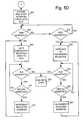
- channel circuit 50loops through tests 500 , 532 , 556 , 560 , for an assertion of SERVO GATE, READ GATE, WRITE GATE, or ALE from disk controller circuit 150 . If none of the aforementioned timing function signals is asserted, channel circuit 50 tests at step 561 for a continuation of an interrupted transmission of user data. If so, operations proceed at connector 5 B- 1 in FIG. 5 B. Starting with step 500 , if SERVO GATE is asserted, then channel circuit 50 is enabled for servo sector demodulating, step 502 .
- channel circuit 50detects a servo sync signal from rotating medium 16 , step 504 and proceeds to assert SYNC DET- (not shown). From this point, a sequence of packets representing servo sector components are transmitted such as described in FIGS. 2, 3 , or 4 above. The sequence of transmission depends on specific implementation, therefore a next step would be either reading track ID step 508 , reading servo bursts step 516 or reading auxiliary data step 524 .
- a packetis placed on unified bus 120 as in step 512 , 520 or 528 , DATA VALID 128 is asserted at step 514 , 522 , or 530 , and de-asserted after an appropriate interval at step 515 , 523 , or 531 .
- step 532If READ GATE 122 is asserted by disk controller circuit 150 , step 532 , then processing moves to connector 2 at step 534 in FIG. 5 B.
- step 534channel circuit 50 is enabled for reading and demodulating user data sectors. Initially, channel circuit 50 detects a data sync signal from rotating media 16 , at step 536 .
- data detection circuit 54begins to process the user data bytes which are received from rotating medium 16 , thus causing a T 2 latency delay for the demodulating process, in step 538 .
- Channel circuit 50then checks for a user data byte available from demodulating circuit 54 at step 540 , indicating the start of demodulated data. If so, the channel circuit 50 places a user data header on the bus at step 542 and asserts the DATA VALID 128 , step 544 . Next, the user data byte is placed on the unified bus 120 , step 546 . While transmitting the data bytes on the unified bus 120 , the channel circuit 50 checks to see if the SERVO GATE 124 has been asserted by the disk controller circuit 150 , step 548 .
- channel circuit 50terminates transmission at step 562 and deasserts data valid.
- channel circuit 50may preferably continue to transmit user data bytes for some period of time after SERVO GATE 124 is asserted in a “hidden flush” operation as there is a window of time until the servo sync mark is detected to continue such transmission.
- step 548If SERVO GATE 124 is not asserted in step 548 , then a check is made to see if all bytes are transferred for the current data sector or data sector segment, step 550 . If not, the loop continues at step 546 . Otherwise, channel circuit 50 deasserts DATA VALID 128 , step 552 . If more data sectors are being processed, step 554 , then processing moves back to step 540 to await the start of a next user data segment.
- step 556processing moves to step 558 in FIG. 5 C.
- channel circuit 50is then enabled for write data encoding and receives write data as shown in FIG. 4 .
- step 560if ALE/CSEL- 130 is asserted by disk controller circuit 150 , step 560 , then processing moves to step 562 in FIG. 5 D.
- Channel circuit 50then latches the register address from the bus, step 562 .
- the channel circuit 50checks to see if REN 132 is asserted, step 564 . If REN 564 is asserted, then channel circuit 50 gates the addressed register data to unified bus 120 , step 566 .
- Channel circuit 50then checks to see if ALE/CSEL- 130 is still asserted, step 568 . If ALE/CSEL- 130 is still asserted, then channel circuit 50 checks to see if REN 122 has been reasserted, step 570 . If REN 122 has been reasserted, then channel circuit 50 increments the register address, step 572 . Processing moves back to step 566 .
- channel circuit 50gates data from unified bus 120 to the addressed register, step 576 .
- Channel circuit 50then checks to see if ALE/CSEL- 130 is still asserted, step 578 . If not, then transfer of the register data is ended, step 580 . Otherwise, channel circuit 50 checks to see if WEN- 132 is reasserted, step 582 . If WEN- 132 is reasserted, the register address is incremented, step 584 , and processing moves back to step 576 .
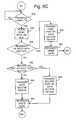
- a flowchart illustrating disk controller circuit 150 operationis shown.
- a timerwhich is synchronous with rotating disk 16 is employed to define time intervals for reading or writing data on rotating disk 16 .
- disk controller circuit 150asserts SERVO GATE 124 , step 604 .
- disk controller circuit 150then waits for SYNC DET- 136 to be asserted by channel circuit 50 before proceeding. If SYNC DET- 136 is not asserted, the disk drive will revert to various error recovery procedures which are well known in the art.
- disk controller circuit 150reads the header byte, step 608 , which identifies the type of servo data being received from channel circuit 50 . If the header indicates that a TIM packet is being transmitted from channel circuit 50 , step 610 , then the TID packet is read from unified bus 120 and stored in a TID register, step 612 . Processing then loops back to connector 6 A 3 at step 608 .
- step 614disk controller circuit 150 reads the servo burst packet and stores it in a servo burst register step 616 . Processing then loops back to step 608 via connector 6 A 3 .
- disk controller circuit 150If the header indicates that auxiliary servo data is being transmitted, step 618 , then disk controller circuit 150 reads the auxiliary servo data and stores it in a register for the specific type of auxiliary servo data that is being received, step 620 . Processing then loops back to step 606 .
- disk controller circuit 150de-asserts SERVO GATE 124 , step 624 .
- the examples illustrated hereinshow the servo wedge components 208 A, 208 B and 208 C being transmitted as separate packets, in an alternate embodiment the components can be transmitted in a single packet with or without intervening headers. In these or other embodiments, the servo wedge components can be transmitted in a different order than that shown.
- disk controller 150If it is time for channel circuit 50 to read a data sector, step 626 , then disk controller 150 asserts READ GATE 122 , step 628 , to enable channel circuit 50 to receive a data sector as explained with respect to FIGS. 5A-5B above.
- step 630If it is time to write a user data sector to rotating disk 16 , step 630 , WRITE GATE signal 132 is asserted at step 632 . Processing then moves to step 634 in FIG. 6 C.
- step 634disk controller circuit 150 delays placing data on unified bus 120 while channel circuit 50 is writing a preamble segment on the media. During this preamble period, data from a previous operation may be placed on unified bus 120 by channel circuit 50 to perform another type of “bidden flush” where data transfer on the unified bus overlaps the writing of the data sector preamble. Otherwise, at the appropriate time, disk controller circuit 150 places a data sync byte code on unified bus 120 to instruct channel 50 to write a data sync mark on disk 16 .
- disk controller circuit 150transmits the first part of the data sector on unified bus 120 , step 638 .
- WRITE GATE 132is then deasserted, step 640 .
- disk controller circuit 150transmits the second part of the data sector on unified bus 120 , step 644 . Otherwise, disk controller circuit 150 transmits the entire data sector on unified bus 120 , step 646 .
- Disk controller circuit 150then deasserts WRITE GATE 132 step 648 , and processing returns to step 600 in FIG. 6 A.
- disk controller circuit 150If disk controller circuit 150 requires transmission of register data on unified bus 120 , step 652 , disk controller 150 transmits the register address, step 654 . Disk controller circuit 150 asserts ALE/CSEL- 130 , step 656 . Depending on whether register data is to be read from a channel circuit 50 register stack 64 , or transmitted from the image of register data 154 in disk controller circuit 150 to register stack 64 , disk controller circuit 150 asserts either REN 122 or WEN- 132 , step 658 . Disk controller circuit 150 then reads or writes register data from or to unified bus 120 , step 660 as explained with respect to FIG. 3 above.
- step 662disk controller circuit 150 reads the user data header byte from NRZ DATA BUS 134 of unified bus 120 . Disk controller circuit 150 determines if the data packet is the beginning of a demodulated data sector, step 664 . If the data packet does represent the first part of a data sector, disk controller circuit 150 resets a byte counter to 0, step 666 . Disk controller circuit 150 then adds the byte to a user data buffer, step 668 . Disk controller circuit 150 checks the timer to determine if it is time for a servo sector to be processed, step 670 .
- step 672processing moves back to step 668 . If the last data byte plus error correction codes have been received, then the data sector received is released to the host, step 674 .
Landscapes
- Engineering & Computer Science (AREA)
- Signal Processing (AREA)
- Signal Processing For Digital Recording And Reproducing (AREA)
Abstract
Description
Claims (21)
Priority Applications (1)
| Application Number | Priority Date | Filing Date | Title |
|---|---|---|---|
| US09/489,856US6415349B1 (en) | 2000-01-24 | 2000-01-24 | Disk drive with unified channel-disk controller bus for transmitting user data, servo data, and register data |
Applications Claiming Priority (1)
| Application Number | Priority Date | Filing Date | Title |
|---|---|---|---|
| US09/489,856US6415349B1 (en) | 2000-01-24 | 2000-01-24 | Disk drive with unified channel-disk controller bus for transmitting user data, servo data, and register data |
Publications (1)
| Publication Number | Publication Date |
|---|---|
| US6415349B1true US6415349B1 (en) | 2002-07-02 |
Family
ID=23945547
Family Applications (1)
| Application Number | Title | Priority Date | Filing Date |
|---|---|---|---|
| US09/489,856Expired - LifetimeUS6415349B1 (en) | 2000-01-24 | 2000-01-24 | Disk drive with unified channel-disk controller bus for transmitting user data, servo data, and register data |
Country Status (1)
| Country | Link |
|---|---|
| US (1) | US6415349B1 (en) |
Cited By (150)
| Publication number | Priority date | Publication date | Assignee | Title |
|---|---|---|---|---|
| US20040057145A1 (en)* | 2002-09-20 | 2004-03-25 | Fung Kendall H. | NRZ pipeline servo while reading or writing |
| US20050154823A1 (en)* | 2001-09-14 | 2005-07-14 | Bruner Curtis H. | Digital device configuration and method |
| US20050160195A1 (en)* | 2001-09-14 | 2005-07-21 | Bruner Curtis H. | Digital device configuration and method |
| US20050182875A1 (en)* | 2001-09-14 | 2005-08-18 | Bruner Curtis H. | Digital device configuration and method |
| US20060203498A1 (en)* | 2005-03-08 | 2006-09-14 | Vincent Lin | Multi-colored light bulb cover |
| US20080049350A1 (en)* | 2006-08-22 | 2008-02-28 | Bruner Curtis H | Disk drive with multi-protocol channel to controller interface and method |
| US20090063922A1 (en)* | 2007-08-31 | 2009-03-05 | Gower Kevin C | System for Performing Error Correction Operations in a Memory Hub Device of a Memory Module |
| US20090063784A1 (en)* | 2007-08-31 | 2009-03-05 | Gower Kevin C | System for Enhancing the Memory Bandwidth Available Through a Memory Module |
| US20090063761A1 (en)* | 2007-08-31 | 2009-03-05 | Gower Kevin C | Buffered Memory Module Supporting Two Independent Memory Channels |
| US20090063729A1 (en)* | 2007-08-31 | 2009-03-05 | Gower Kevin C | System for Supporting Partial Cache Line Read Operations to a Memory Module to Reduce Read Data Traffic on a Memory Channel |
| US20090063787A1 (en)* | 2007-08-31 | 2009-03-05 | Gower Kevin C | Buffered Memory Module with Multiple Memory Device Data Interface Ports Supporting Double the Memory Capacity |
| US20090063923A1 (en)* | 2007-08-31 | 2009-03-05 | Gower Kevin C | System and Method for Performing Error Correction at a Memory Device Level that is Transparent to a Memory Channel |
| US20090063731A1 (en)* | 2007-09-05 | 2009-03-05 | Gower Kevin C | Method for Supporting Partial Cache Line Read and Write Operations to a Memory Module to Reduce Read and Write Data Traffic on a Memory Channel |
| US20090063730A1 (en)* | 2007-08-31 | 2009-03-05 | Gower Kevin C | System for Supporting Partial Cache Line Write Operations to a Memory Module to Reduce Write Data Traffic on a Memory Channel |
| US20090190427A1 (en)* | 2008-01-24 | 2009-07-30 | Brittain Mark A | System to Enable a Memory Hub Device to Manage Thermal Conditions at a Memory Device Level Transparent to a Memory Controller |
| US20090193200A1 (en)* | 2008-01-24 | 2009-07-30 | Brittain Mark A | System to Support a Full Asynchronous Interface within a Memory Hub Device |
| US20090193201A1 (en)* | 2008-01-24 | 2009-07-30 | Brittain Mark A | System to Increase the Overall Bandwidth of a Memory Channel By Allowing the Memory Channel to Operate at a Frequency Independent from a Memory Device Frequency |
| US20090193203A1 (en)* | 2008-01-24 | 2009-07-30 | Brittain Mark A | System to Reduce Latency by Running a Memory Channel Frequency Fully Asynchronous from a Memory Device Frequency |
| US20090193315A1 (en)* | 2008-01-24 | 2009-07-30 | Gower Kevin C | System for a Combined Error Correction Code and Cyclic Redundancy Check Code for a Memory Channel |
| US20090193290A1 (en)* | 2008-01-24 | 2009-07-30 | Arimilli Ravi K | System and Method to Use Cache that is Embedded in a Memory Hub to Replace Failed Memory Cells in a Memory Subsystem |
| KR100943855B1 (en)* | 2006-06-01 | 2010-02-24 | 브로드콤 코포레이션 | Disk controllers, channel interfaces and how to use them |
| US20110004709A1 (en)* | 2007-09-05 | 2011-01-06 | Gower Kevin C | Method for Enhancing the Memory Bandwidth Available Through a Memory Module |
| US7899983B2 (en) | 2007-08-31 | 2011-03-01 | International Business Machines Corporation | Buffered memory module supporting double the memory device data width in the same physical space as a conventional memory module |
| US7930469B2 (en) | 2008-01-24 | 2011-04-19 | International Business Machines Corporation | System to provide memory system power reduction without reducing overall memory system performance |
| US20110226729A1 (en)* | 2007-11-01 | 2011-09-22 | Western Digital Technologies, Inc. | Method of manufacturing a double sided flex circuit for a disk drive wherein a first side lead provides an etching mask for a second side lead |
| US20130044388A1 (en)* | 2011-08-18 | 2013-02-21 | Hon Hai Precision Industry Co., Ltd. | Voltage adjustment circuit for storage media |
| US8879188B1 (en) | 2010-08-23 | 2014-11-04 | Western Digital Technologies, Inc. | Disk drive employing fly height calibration tracks to account for magnetic entropy and thermal decay |
| US8891341B1 (en) | 2013-03-11 | 2014-11-18 | Western Digital Technologies, Inc. | Energy assisted magnetic recording disk drive using modulated laser light |
| US8891193B1 (en) | 2013-05-09 | 2014-11-18 | Western Digital Technologies, Inc. | Disk drive calibrating threshold and gain of touchdown sensor |
| US8902527B1 (en) | 2010-03-22 | 2014-12-02 | Western Digital Technologies, Inc. | Systems and methods for improving sequential data rate performance using sorted data zones |
| US8902529B1 (en) | 2012-11-20 | 2014-12-02 | Western Digital Technologies, Inc. | Dual frequency crystal oscillator |
| US8908311B1 (en) | 2014-01-27 | 2014-12-09 | Western Digital Technologies, Inc. | Data storage device writing a multi-sector codeword in segments over multiple disk revolutions |
| US8909889B1 (en) | 2011-10-10 | 2014-12-09 | Western Digital Technologies, Inc. | Method and apparatus for servicing host commands by a disk drive |
| US8914625B1 (en) | 2009-07-31 | 2014-12-16 | Western Digital Technologies, Inc. | Automatically configuring a web browser file when booting an operating system from a data storage device |
| US8922939B1 (en) | 2013-04-02 | 2014-12-30 | Western Digital Technologies, Inc. | Disk drive generating feed-forward fly height control based on temperature sensitive fly height sensor |
| US8937782B1 (en) | 2012-05-07 | 2015-01-20 | Western Digital Technologies, Inc. | Hard disk drive assembly including a NVSM to store configuration data for controlling disk drive operations |
| US8941941B1 (en) | 2013-02-28 | 2015-01-27 | Western Digital Technologies, Inc. | Disk drive calibrating touchdown sensor |
| US8947812B1 (en) | 2014-03-27 | 2015-02-03 | Western Digital Technologies, Inc. | Data storage device comprising equalizer filter and inter-track interference filter |
| US8949521B1 (en) | 2013-04-10 | 2015-02-03 | Western Digital Technologies, Inc. | Actuator prepositioning for disk drive |
| US8953277B1 (en) | 2014-06-16 | 2015-02-10 | Western Digital Technologies, Inc. | Data storage device writing tracks on a disk with equal spacing |
| US8954664B1 (en) | 2010-10-01 | 2015-02-10 | Western Digital Technologies, Inc. | Writing metadata files on a disk |
| US8953269B1 (en) | 2014-07-18 | 2015-02-10 | Western Digital Technologies, Inc. | Management of data objects in a data object zone |
| US8959281B1 (en) | 2012-11-09 | 2015-02-17 | Western Digital Technologies, Inc. | Data management for a storage device |
| US8958167B1 (en) | 2013-12-23 | 2015-02-17 | Western Digital Technologies, Inc. | Detection of disk surface irregularities in data storage devices |
| US8970978B1 (en) | 2012-10-22 | 2015-03-03 | Western Digital Technologies, Inc. | Disk drive detecting head touchdown by applying DC+AC control signal to fly height actuator |
| US8976633B1 (en) | 2014-04-15 | 2015-03-10 | Western Digital Technologies, Inc. | Data storage device calibrating fly height actuator based on laser power for heat assisted magnetic recording |
| US8988809B1 (en) | 2014-02-18 | 2015-03-24 | Western Digital (Fremont), Llc | Disk recording device for writing a radially coherent reference band by measuring relative timing offsets of reference bursts |
| US8990493B1 (en) | 2011-06-30 | 2015-03-24 | Western Digital Technologies, Inc. | Method and apparatus for performing force unit access writes on a disk |
| US8988810B1 (en) | 2014-04-16 | 2015-03-24 | Western Digital Technologies, Inc. | Track measurement for data storage device |
| US8996839B1 (en) | 2012-01-23 | 2015-03-31 | Western Digital Technologies, Inc. | Data storage device aligning partition to boundary of sector when partition offset correlates with offset of write commands |
| US9001453B1 (en) | 2014-07-18 | 2015-04-07 | Western Digital Technologies, Inc. | Data storage device calibrating fly height actuator based on read mode touchdown resistance of touchdown sensor |
| US9009358B1 (en) | 2008-09-23 | 2015-04-14 | Western Digital Technologies, Inc. | Configuring a data storage device with a parameter file interlocked with configuration code |
| US9013818B1 (en) | 2013-12-06 | 2015-04-21 | Western Digital Technologies, Inc. | Disk drive measuring reader/writer gap by measuring fractional clock cycle over disk radius |
| US9013821B1 (en) | 2014-06-10 | 2015-04-21 | Western Digital Technologies, Inc. | Data storage device employing one-dimensional and two-dimensional channels |
| US9021410B1 (en) | 2013-12-10 | 2015-04-28 | Western Technologies, Inc. | Electronic system with multi-cycle simulation coverage mechanism and method of operation thereof |
| US20150120981A1 (en)* | 2013-10-25 | 2015-04-30 | Lsi Corporation | Data Interface for Point-to-Point Communications Between Devices |
| US9025270B1 (en) | 2013-09-17 | 2015-05-05 | Western Digital Technologies, Inc. | Electronic system with current conservation mechanism and method of operation thereof |
| US9025421B1 (en) | 2014-10-08 | 2015-05-05 | Western Digital Technologies, Inc. | Data storage device adjusting laser input power to compensate for temperature variations |
| US9025267B1 (en) | 2014-06-09 | 2015-05-05 | Western Digital Technologies, Inc. | Data storage device using branch metric from adjacent track to compensate for inter-track interference |
| US9047917B1 (en) | 2013-11-26 | 2015-06-02 | Western Digital Technologies, Inc. | Disk drive slider with sense amplifier for coupling to a preamp through a supply/bias line and a read signal line |
| US9049471B2 (en) | 2001-10-17 | 2015-06-02 | Keen Personal Media, Inc. | Personal video recorder for inserting a stored advertisement into a displayed broadcast stream |
| US9053749B1 (en) | 2013-03-15 | 2015-06-09 | Western Digital Technologies, Inc. | Disk drive comprising a per-drive and per-head fly height filter |
| US9053730B1 (en) | 2012-05-11 | 2015-06-09 | Western Digital Technologies, Inc. | Disk drive comprising extended range head proximity sensor |
| US9064525B2 (en) | 2013-11-26 | 2015-06-23 | Western Digital Technologies, Inc. | Disk drive comprising laser transmission line optimized for heat assisted magnetic recording |
| US9064542B1 (en) | 2013-04-08 | 2015-06-23 | Western Digital Technologies, Inc. | Scheduled load of heads to reduce lubricant migration on pole tip and decrease time to ready |
| US9064504B1 (en) | 2014-01-29 | 2015-06-23 | Western Digital Technologies, Inc. | Electronic system with media recovery mechanism and method of operation thereof |
| US9063838B1 (en) | 2012-01-23 | 2015-06-23 | Western Digital Technologies, Inc. | Data storage device shifting data chunks of alignment zone relative to sector boundaries |
| US9070406B1 (en) | 2014-03-10 | 2015-06-30 | Western Digital Technologies, Inc. | Disk drive configuring one-dimensional and two-dimensional recording areas based on read element spacing |
| US9076474B1 (en) | 2014-12-23 | 2015-07-07 | Western Digital Technologies, Inc. | Data storage device attenuating thermal decay effect on fly height measurement |
| US9074941B1 (en) | 2013-03-14 | 2015-07-07 | Western Digital Technologies, Inc. | Systems and methods for measuring ambient and laser temperature in heat assisted magnetic recording |
| US9075714B1 (en) | 2014-05-13 | 2015-07-07 | Western Digital Technologies, Inc. | Electronic system with data management mechanism and method of operation thereof |
| US9082458B1 (en) | 2014-03-10 | 2015-07-14 | Western Digital Technologies, Inc. | Data storage device balancing and maximizing quality metric when configuring arial density of each disk surface |
| US9099103B1 (en) | 2014-10-21 | 2015-08-04 | Western Digital Technologies, Inc. | Heat assisted magnetic recording withinterlaced high-power heated and low-power heated tracks |
| US9099134B1 (en) | 2015-01-27 | 2015-08-04 | Western Digital Technologies, Inc. | Data storage device employing multiple jog profiles for a butterfly written disk surface |
| US9099144B1 (en) | 2013-10-11 | 2015-08-04 | Western Digital Technologies, Inc. | Disk drive evaluating laser performance for heat assisted magnetic recording |
| US9117463B1 (en) | 2014-06-23 | 2015-08-25 | Western Digital Technologies, Inc. | Data storage device erasing multiple adjacent data tracks to recover from inter-track interference |
| US9117479B1 (en) | 2014-09-24 | 2015-08-25 | Western Digital Technologies, Inc. | Data storage device calibrating laser write power for heat assisted magnetic recording |
| US9117489B1 (en) | 2014-02-18 | 2015-08-25 | Western Digital Technologies, Inc. | Data storage device screening heads by verifying defects after defect scan |
| US9123382B1 (en) | 2014-10-28 | 2015-09-01 | Western Digital Technologies, Inc. | Non-volatile caching for sequence of data |
| US9123370B1 (en) | 2014-04-15 | 2015-09-01 | Western Digital Technologies, Inc. | Data storage device calibrating fly height actuator based on laser power for heat assisted magnetic recording |
| US9129628B1 (en) | 2014-10-23 | 2015-09-08 | Western Digital Technologies, Inc. | Data management for data storage device with different track density regions |
| US9128820B1 (en) | 2012-06-18 | 2015-09-08 | Western Digital Technologies, Inc. | File management among different zones of storage media |
| US9135205B1 (en) | 2013-05-01 | 2015-09-15 | Western Digital Technologies, Inc. | Data storage assembly for archive cold storage |
| US9153287B1 (en) | 2013-05-13 | 2015-10-06 | Western Digital Technologies, Inc. | Data access for shingled magnetic recording media |
| US9153266B1 (en) | 2014-09-11 | 2015-10-06 | Western Digital Technologies, Inc. | Data storage device measuring laser protrusion fly height profile |
| US9158722B1 (en) | 2011-11-02 | 2015-10-13 | Western Digital Technologies, Inc. | Data storage device to communicate with a host in a SATA or a USB mode |
| US9164694B1 (en) | 2013-06-19 | 2015-10-20 | Western Digital Technologies, Inc. | Data storage device detecting read-before-write conditions and returning configurable return data |
| US9171575B1 (en) | 2014-06-23 | 2015-10-27 | Western Digital Technologies, Inc. | Data storage device detecting media defects by writing opposite polarity test pattern |
| US9183864B1 (en) | 2013-06-13 | 2015-11-10 | Western Digital Technologies, Inc. | Disk drive adjusting closed-loop fly height target based on change in open-loop fly height control signal |
| US9183877B1 (en) | 2015-03-20 | 2015-11-10 | Western Digital Technologies, Inc. | Data storage device comprising two-dimensional data dependent noise whitening filters for two-dimensional recording |
| US9189392B1 (en) | 2011-06-30 | 2015-11-17 | Western Digital Technologies, Inc. | Opportunistic defragmentation during garbage collection |
| US9196302B1 (en) | 2015-03-18 | 2015-11-24 | Western Digital Technologies, Inc. | Electronic system with media maintenance mechanism and method of operation thereof |
| US9214186B1 (en) | 2015-03-23 | 2015-12-15 | Western Digital Technologies, Inc. | Data storage device measuring radial offset between read element and write element |
| US9213493B1 (en) | 2011-12-16 | 2015-12-15 | Western Digital Technologies, Inc. | Sorted serpentine mapping for storage drives |
| US9230585B1 (en) | 2014-01-31 | 2016-01-05 | Western Digital Technologies, Inc. | Per wedge preheat DFH to improve data storage device performance |
| US9230605B1 (en) | 2014-12-01 | 2016-01-05 | Western Digital Technologies, Inc. | Data storage device maximizing areal density based on a target quality metric |
| US9236086B1 (en) | 2014-10-15 | 2016-01-12 | Western Digital Technologies, Inc. | Methods for reducing operational latency of data storage systems |
| US9245556B2 (en) | 2014-03-10 | 2016-01-26 | Western Digital Technologies, Inc. | Disk drive employing multiple read elements to increase radial band for two-dimensional magnetic recording |
| US9245558B1 (en) | 2014-05-09 | 2016-01-26 | Western Digital Technologies, Inc. | Electronic system with data management mechanism and method of operation thereof |
| US9251844B1 (en) | 2014-06-02 | 2016-02-02 | Western Digital Technologies, Inc. | Waterfall method and apparatus for a data storage device read system |
| US9251856B1 (en) | 2014-05-30 | 2016-02-02 | Western Digial Technologies, Inc. | Read failover method and apparatus for a data storage system |
| US9257145B1 (en) | 2013-11-27 | 2016-02-09 | Western Digital Technologies, Inc. | Disk drive measuring down-track spacing of read sensors |
| US9257146B1 (en) | 2014-02-11 | 2016-02-09 | Western Digital Technologies, Inc. | Data storage device comprising sequence detector compensating for inter-track interference |
| US9257143B1 (en) | 2014-12-23 | 2016-02-09 | Western Digital Technologies, Inc. | Precautionary measures for data storage device environmental conditions |
| US9263088B2 (en) | 2014-03-21 | 2016-02-16 | Western Digital Technologies, Inc. | Data management for a data storage device using a last resort zone |
| US9268649B1 (en) | 2011-06-23 | 2016-02-23 | Western Digital Technologies, Inc. | Disk drive with recent write streams list for data refresh determination |
| US9269393B1 (en) | 2014-12-08 | 2016-02-23 | Western Digital Technologies, Inc. | Electronic system with data refresh mechanism and method of operation thereof |
| US9268499B1 (en) | 2010-08-13 | 2016-02-23 | Western Digital Technologies, Inc. | Hybrid drive migrating high workload data from disk to non-volatile semiconductor memory |
| US9281009B1 (en) | 2014-12-18 | 2016-03-08 | Western Digital Technologies, Inc. | Data storage device employing variable size interleave written track segments |
| US9311939B1 (en) | 2014-12-23 | 2016-04-12 | Western Digital Technologies, Inc. | Write-through media caching |
| US9318137B1 (en) | 2015-03-13 | 2016-04-19 | Western Digital Technologies, Inc. | Data storage device executing retry operation by buffering signal samples at different radial offsets |
| US9330715B1 (en) | 2010-03-22 | 2016-05-03 | Western Digital Technologies, Inc. | Mapping of shingled magnetic recording media |
| US9355666B1 (en) | 2013-09-30 | 2016-05-31 | Western Digital Technologies, Inc. | Disk drive measuring stroke difference between heads by detecting a difference between ramp contact |
| US9361938B1 (en) | 2015-04-16 | 2016-06-07 | Western Digital Technologies, Inc. | Disk defect management for a data storage device |
| US9368131B1 (en) | 2015-04-03 | 2016-06-14 | Western Digital (Fremont), Llc | Data storage device employing mirrored cross-track profiles for top and bottom disk surfaces |
| US9368132B1 (en) | 2015-09-04 | 2016-06-14 | Western Digital Technologies, Inc. | Data storage device employing differential write data signal and differential write pattern signal |
| US9383923B1 (en) | 2012-10-18 | 2016-07-05 | Western Digital Technologies, Inc. | Write pointer management for a disk drive |
| US9401165B1 (en) | 2014-05-05 | 2016-07-26 | Western Digital Technologies, Inc. | Method and system to monitor magnetic head loading and unloading stability for a data storage system |
| US9417628B2 (en) | 2013-03-13 | 2016-08-16 | Western Digital Technologies, Inc. | Production failure analysis system |
| US9424864B2 (en) | 2014-07-02 | 2016-08-23 | Western Digital Technologies, Inc. | Data management for a data storage device with zone relocation |
| US9437242B1 (en) | 2015-09-14 | 2016-09-06 | Western Digital Technologies, Inc. | Data storage device employing different frequency preambles in adjacent data tracks |
| US9466321B1 (en) | 2015-06-05 | 2016-10-11 | Western Digital Technologies, Inc. | Angular position tracking of data accesses to mitigate risk of data loss |
| US9466318B2 (en) | 2014-12-24 | 2016-10-11 | Western Digital Technologies, Inc. | Allowing fast data zone switches on data storage devices |
| US9472219B1 (en) | 2015-05-01 | 2016-10-18 | Western Digital Technologies, Inc. | Data storage device calibrating parameter for heat assisted magnetic recording |
| US9502068B1 (en) | 2015-04-08 | 2016-11-22 | Western Digital Technologies, Inc. | Data storage device updating laser power during non-write mode for heat assisted magnetic recording |
| US9501393B2 (en) | 2014-01-27 | 2016-11-22 | Western Digital Technologies, Inc. | Data storage system garbage collection based on at least one attribute |
| US9588898B1 (en) | 2015-06-02 | 2017-03-07 | Western Digital Technologies, Inc. | Fullness control for media-based cache operating in a steady state |
| US9600205B1 (en) | 2014-09-22 | 2017-03-21 | Western Digital Technologies, Inc. | Power aware power safe write buffer |
| US9632711B1 (en) | 2014-04-07 | 2017-04-25 | Western Digital Technologies, Inc. | Processing flush requests by utilizing storage system write notifications |
| US9639287B1 (en) | 2015-06-29 | 2017-05-02 | Western Digital Technologies, Inc. | Write command reporting |
| US9645752B1 (en) | 2014-04-07 | 2017-05-09 | Western Digital Technologies, Inc. | Identification of data committed to non-volatile memory by use of notification commands |
| US9672107B1 (en) | 2015-02-11 | 2017-06-06 | Western Digital Technologies, Inc. | Data protection for a data storage device |
| US9747928B1 (en) | 2014-09-25 | 2017-08-29 | Western Digital Technologies, Inc. | Data storage device modifying write operation when a laser mode hop is detected |
| US9761273B1 (en) | 2015-11-03 | 2017-09-12 | Western Digital Technologies, Inc. | Data storage device encoding and interleaving codewords to improve trellis sequence detection |
| US9842617B1 (en) | 2015-06-29 | 2017-12-12 | Western Digital Technologies, Inc. | Electronic system with head management mechanism and method of operation thereof |
| US9842622B1 (en) | 2014-12-23 | 2017-12-12 | Western Digital Technologies, Inc. | Data storage device having improved read failure tolerance |
| US9864529B1 (en) | 2014-01-27 | 2018-01-09 | Western Digital Technologies, Inc. | Host compatibility for host managed storage media |
| US9870281B1 (en) | 2015-03-20 | 2018-01-16 | Western Digital Technologies, Inc. | Power loss mitigation for data storage device |
| US9875055B1 (en) | 2014-08-04 | 2018-01-23 | Western Digital Technologies, Inc. | Check-pointing of metadata |
| US9916616B2 (en) | 2014-03-31 | 2018-03-13 | Western Digital Technologies, Inc. | Inventory management system using incremental capacity formats |
| US9933955B1 (en) | 2015-03-05 | 2018-04-03 | Western Digital Technologies, Inc. | Power safe write buffer for data storage device |
| US9952950B1 (en) | 2014-09-08 | 2018-04-24 | Western Digital Technologies, Inc. | Data management in RAID environment |
| US9959052B1 (en) | 2015-09-17 | 2018-05-01 | Western Digital Technologies, Inc. | Media based cache for data storage device |
| US10020012B1 (en)* | 2017-10-31 | 2018-07-10 | Seagate Technology Llc | Data storage drive with low-latency ports coupling multiple servo control processors |
| US10056920B1 (en) | 2015-11-03 | 2018-08-21 | Western Digital Technologies, Inc. | Data storage device encoding and interleaving codewords to improve trellis sequence detection |
| US10063257B1 (en) | 2015-11-03 | 2018-08-28 | Western Digital Technologies, Inc. | Data storage device encoding and interleaving codewords to improve trellis sequence detection |
| US10282371B1 (en) | 2014-12-02 | 2019-05-07 | Western Digital Technologies, Inc. | Object storage device with probabilistic data structure |
| US10282096B1 (en) | 2014-12-17 | 2019-05-07 | Western Digital Technologies, Inc. | Identification of data with predetermined data pattern |
| US10365836B1 (en) | 2015-01-27 | 2019-07-30 | Western Digital Technologies, Inc. | Electronic system with declustered data protection by parity based on reliability and method of operation thereof |
| US11417361B2 (en)* | 2020-08-19 | 2022-08-16 | Marvell Asia Pte, Ltd. | Write timing for RRO field in a constant density servo system |
Citations (4)
| Publication number | Priority date | Publication date | Assignee | Title |
|---|---|---|---|---|
| US5341249A (en)* | 1992-08-27 | 1994-08-23 | Quantum Corporation | Disk drive using PRML class IV sampling data detection with digital adaptive equalization |
| US5606466A (en) | 1995-10-23 | 1997-02-25 | Quantum Corporation | Method for overlapping block read events in disk drive |
| US5829011A (en) | 1997-01-31 | 1998-10-27 | Texas Instruments Incorporated | Apparatus and method of exchanging data and operational parameters in a mass storage system |
| US6178056B1 (en)* | 1997-03-11 | 2001-01-23 | Western Digital Corporation | Disk drive employing state variable trap registers for providing stored servo and user data state variables to sampled-data channel |
- 2000
- 2000-01-24USUS09/489,856patent/US6415349B1/ennot_activeExpired - Lifetime
Patent Citations (5)
| Publication number | Priority date | Publication date | Assignee | Title |
|---|---|---|---|---|
| US5341249A (en)* | 1992-08-27 | 1994-08-23 | Quantum Corporation | Disk drive using PRML class IV sampling data detection with digital adaptive equalization |
| US5606466A (en) | 1995-10-23 | 1997-02-25 | Quantum Corporation | Method for overlapping block read events in disk drive |
| US5829011A (en) | 1997-01-31 | 1998-10-27 | Texas Instruments Incorporated | Apparatus and method of exchanging data and operational parameters in a mass storage system |
| US6178056B1 (en)* | 1997-03-11 | 2001-01-23 | Western Digital Corporation | Disk drive employing state variable trap registers for providing stored servo and user data state variables to sampled-data channel |
| US6278568B1 (en)* | 1997-03-11 | 2001-08-21 | Western Digital | Disk drive employing read channel IC with common port for data and servo |
Cited By (204)
| Publication number | Priority date | Publication date | Assignee | Title |
|---|---|---|---|---|
| US7165139B2 (en) | 2001-09-14 | 2007-01-16 | Cornice, Inc. | Digital device configuration and method |
| US7149891B2 (en) | 2001-09-14 | 2006-12-12 | Cornice, Inc. | Digital device configuration and method |
| US20050160220A1 (en)* | 2001-09-14 | 2005-07-21 | Bruner Curtis H. | Digital device configuration and method |
| US20050160195A1 (en)* | 2001-09-14 | 2005-07-21 | Bruner Curtis H. | Digital device configuration and method |
| US20050166015A1 (en)* | 2001-09-14 | 2005-07-28 | Bruner Curtis H. | Digital device configuration and method |
| US20050182875A1 (en)* | 2001-09-14 | 2005-08-18 | Bruner Curtis H. | Digital device configuration and method |
| US20050180054A1 (en)* | 2001-09-14 | 2005-08-18 | Bruner Curtis H. | Digital device configuration and method |
| US20050195514A1 (en)* | 2001-09-14 | 2005-09-08 | Bruner Curtis H. | Digital device configuration and method |
| US7162577B2 (en)* | 2001-09-14 | 2007-01-09 | Cornice, Inc. | Digital device configuration and method |
| US7546411B2 (en) | 2001-09-14 | 2009-06-09 | Bruner Curtis H | Digital device configuration and method |
| US7106541B2 (en) | 2001-09-14 | 2006-09-12 | Convergent Systems Solutions, Llc | Digital device configuration and method |
| US8001321B2 (en) | 2001-09-14 | 2011-08-16 | Benhov Gmbh, Llc | Digital device configuration and method |
| US8312209B2 (en) | 2001-09-14 | 2012-11-13 | Benhov Gmbh, Llc | Digital device configuration and method |
| US7551382B2 (en) | 2001-09-14 | 2009-06-23 | Bruner Curtis H | Digital device configuration and method |
| US20050154823A1 (en)* | 2001-09-14 | 2005-07-14 | Bruner Curtis H. | Digital device configuration and method |
| US7689785B2 (en) | 2001-09-14 | 2010-03-30 | Bruner Curtis H | Digital device configuration and method |
| US20050195515A1 (en)* | 2001-09-14 | 2005-09-08 | Bruner Curtis H. | Digital device configuration and method |
| US7162578B2 (en) | 2001-09-14 | 2007-01-09 | Cornice, Inc. | Digital device configuration and method |
| US7702847B2 (en) | 2001-09-14 | 2010-04-20 | Bruner Curtis H | Digital device configuration and method |
| US8631196B2 (en) | 2001-09-14 | 2014-01-14 | Benhov Gmbh, Llc | Digital device configuration and method |
| US9396746B2 (en) | 2001-09-14 | 2016-07-19 | Benhov Gmbh, Llc | Digital device configuration and method |
| US9940025B2 (en) | 2001-09-14 | 2018-04-10 | Benhov Gmbh, Llc | Digital device configuration and method |
| US9049471B2 (en) | 2001-10-17 | 2015-06-02 | Keen Personal Media, Inc. | Personal video recorder for inserting a stored advertisement into a displayed broadcast stream |
| US20040057145A1 (en)* | 2002-09-20 | 2004-03-25 | Fung Kendall H. | NRZ pipeline servo while reading or writing |
| US7136239B2 (en)* | 2002-09-20 | 2006-11-14 | Seagate Technology Llc | NRZ pipeline servo while reading or writing |
| WO2004100131A3 (en)* | 2003-04-28 | 2006-02-16 | Cornice Inc | Digital device configuration and method |
| US20060203498A1 (en)* | 2005-03-08 | 2006-09-14 | Vincent Lin | Multi-colored light bulb cover |
| KR100943855B1 (en)* | 2006-06-01 | 2010-02-24 | 브로드콤 코포레이션 | Disk controllers, channel interfaces and how to use them |
| US20100220408A1 (en)* | 2006-08-22 | 2010-09-02 | Benhov Gmbh, Llc | Disk drive with multi-protocol channel to controller interface and method |
| US7738204B2 (en)* | 2006-08-22 | 2010-06-15 | Bruner Curtis H | Disk drive with multi-protocol channel to controller interface and method |
| US8508877B2 (en)* | 2006-08-22 | 2013-08-13 | Benhov Gmbh, Llc | Disk drive with multi-protocol channel to controller interface and method |
| US20080049350A1 (en)* | 2006-08-22 | 2008-02-28 | Bruner Curtis H | Disk drive with multi-protocol channel to controller interface and method |
| US20090063729A1 (en)* | 2007-08-31 | 2009-03-05 | Gower Kevin C | System for Supporting Partial Cache Line Read Operations to a Memory Module to Reduce Read Data Traffic on a Memory Channel |
| US7840748B2 (en) | 2007-08-31 | 2010-11-23 | International Business Machines Corporation | Buffered memory module with multiple memory device data interface ports supporting double the memory capacity |
| US20090063922A1 (en)* | 2007-08-31 | 2009-03-05 | Gower Kevin C | System for Performing Error Correction Operations in a Memory Hub Device of a Memory Module |
| US7584308B2 (en) | 2007-08-31 | 2009-09-01 | International Business Machines Corporation | System for supporting partial cache line write operations to a memory module to reduce write data traffic on a memory channel |
| US20090063784A1 (en)* | 2007-08-31 | 2009-03-05 | Gower Kevin C | System for Enhancing the Memory Bandwidth Available Through a Memory Module |
| US8082482B2 (en) | 2007-08-31 | 2011-12-20 | International Business Machines Corporation | System for performing error correction operations in a memory hub device of a memory module |
| US20090063761A1 (en)* | 2007-08-31 | 2009-03-05 | Gower Kevin C | Buffered Memory Module Supporting Two Independent Memory Channels |
| US20090063787A1 (en)* | 2007-08-31 | 2009-03-05 | Gower Kevin C | Buffered Memory Module with Multiple Memory Device Data Interface Ports Supporting Double the Memory Capacity |
| US20090063923A1 (en)* | 2007-08-31 | 2009-03-05 | Gower Kevin C | System and Method for Performing Error Correction at a Memory Device Level that is Transparent to a Memory Channel |
| US8086936B2 (en) | 2007-08-31 | 2011-12-27 | International Business Machines Corporation | Performing error correction at a memory device level that is transparent to a memory channel |
| US7818497B2 (en) | 2007-08-31 | 2010-10-19 | International Business Machines Corporation | Buffered memory module supporting two independent memory channels |
| US20090063730A1 (en)* | 2007-08-31 | 2009-03-05 | Gower Kevin C | System for Supporting Partial Cache Line Write Operations to a Memory Module to Reduce Write Data Traffic on a Memory Channel |
| US7861014B2 (en) | 2007-08-31 | 2010-12-28 | International Business Machines Corporation | System for supporting partial cache line read operations to a memory module to reduce read data traffic on a memory channel |
| US7865674B2 (en) | 2007-08-31 | 2011-01-04 | International Business Machines Corporation | System for enhancing the memory bandwidth available through a memory module |
| US7899983B2 (en) | 2007-08-31 | 2011-03-01 | International Business Machines Corporation | Buffered memory module supporting double the memory device data width in the same physical space as a conventional memory module |
| US20110004709A1 (en)* | 2007-09-05 | 2011-01-06 | Gower Kevin C | Method for Enhancing the Memory Bandwidth Available Through a Memory Module |
| US20090063731A1 (en)* | 2007-09-05 | 2009-03-05 | Gower Kevin C | Method for Supporting Partial Cache Line Read and Write Operations to a Memory Module to Reduce Read and Write Data Traffic on a Memory Channel |
| US7558887B2 (en) | 2007-09-05 | 2009-07-07 | International Business Machines Corporation | Method for supporting partial cache line read and write operations to a memory module to reduce read and write data traffic on a memory channel |
| US8019919B2 (en) | 2007-09-05 | 2011-09-13 | International Business Machines Corporation | Method for enhancing the memory bandwidth available through a memory module |
| US9060420B2 (en) | 2007-11-01 | 2015-06-16 | Western Digitial Technologies, Inc. | Method of manufacturing a double sided flex circuit for a disk drive wherein a first side lead provides an etching mask for a second side lead |
| US20110226729A1 (en)* | 2007-11-01 | 2011-09-22 | Western Digital Technologies, Inc. | Method of manufacturing a double sided flex circuit for a disk drive wherein a first side lead provides an etching mask for a second side lead |
| US8140936B2 (en) | 2008-01-24 | 2012-03-20 | International Business Machines Corporation | System for a combined error correction code and cyclic redundancy check code for a memory channel |
| US20090190427A1 (en)* | 2008-01-24 | 2009-07-30 | Brittain Mark A | System to Enable a Memory Hub Device to Manage Thermal Conditions at a Memory Device Level Transparent to a Memory Controller |
| US7930470B2 (en) | 2008-01-24 | 2011-04-19 | International Business Machines Corporation | System to enable a memory hub device to manage thermal conditions at a memory device level transparent to a memory controller |
| US7925825B2 (en) | 2008-01-24 | 2011-04-12 | International Business Machines Corporation | System to support a full asynchronous interface within a memory hub device |
| US7925826B2 (en) | 2008-01-24 | 2011-04-12 | International Business Machines Corporation | System to increase the overall bandwidth of a memory channel by allowing the memory channel to operate at a frequency independent from a memory device frequency |
| US20090193315A1 (en)* | 2008-01-24 | 2009-07-30 | Gower Kevin C | System for a Combined Error Correction Code and Cyclic Redundancy Check Code for a Memory Channel |
| US7925824B2 (en) | 2008-01-24 | 2011-04-12 | International Business Machines Corporation | System to reduce latency by running a memory channel frequency fully asynchronous from a memory device frequency |
| US20090193201A1 (en)* | 2008-01-24 | 2009-07-30 | Brittain Mark A | System to Increase the Overall Bandwidth of a Memory Channel By Allowing the Memory Channel to Operate at a Frequency Independent from a Memory Device Frequency |
| US7770077B2 (en) | 2008-01-24 | 2010-08-03 | International Business Machines Corporation | Using cache that is embedded in a memory hub to replace failed memory cells in a memory subsystem |
| US7930469B2 (en) | 2008-01-24 | 2011-04-19 | International Business Machines Corporation | System to provide memory system power reduction without reducing overall memory system performance |
| US20090193290A1 (en)* | 2008-01-24 | 2009-07-30 | Arimilli Ravi K | System and Method to Use Cache that is Embedded in a Memory Hub to Replace Failed Memory Cells in a Memory Subsystem |
| US20090193203A1 (en)* | 2008-01-24 | 2009-07-30 | Brittain Mark A | System to Reduce Latency by Running a Memory Channel Frequency Fully Asynchronous from a Memory Device Frequency |
| US20090193200A1 (en)* | 2008-01-24 | 2009-07-30 | Brittain Mark A | System to Support a Full Asynchronous Interface within a Memory Hub Device |
| US9009358B1 (en) | 2008-09-23 | 2015-04-14 | Western Digital Technologies, Inc. | Configuring a data storage device with a parameter file interlocked with configuration code |
| US8914625B1 (en) | 2009-07-31 | 2014-12-16 | Western Digital Technologies, Inc. | Automatically configuring a web browser file when booting an operating system from a data storage device |
| US8902527B1 (en) | 2010-03-22 | 2014-12-02 | Western Digital Technologies, Inc. | Systems and methods for improving sequential data rate performance using sorted data zones |
| US9330715B1 (en) | 2010-03-22 | 2016-05-03 | Western Digital Technologies, Inc. | Mapping of shingled magnetic recording media |
| US9268499B1 (en) | 2010-08-13 | 2016-02-23 | Western Digital Technologies, Inc. | Hybrid drive migrating high workload data from disk to non-volatile semiconductor memory |
| US8879188B1 (en) | 2010-08-23 | 2014-11-04 | Western Digital Technologies, Inc. | Disk drive employing fly height calibration tracks to account for magnetic entropy and thermal decay |
| US8954664B1 (en) | 2010-10-01 | 2015-02-10 | Western Digital Technologies, Inc. | Writing metadata files on a disk |
| US9268649B1 (en) | 2011-06-23 | 2016-02-23 | Western Digital Technologies, Inc. | Disk drive with recent write streams list for data refresh determination |
| US9189392B1 (en) | 2011-06-30 | 2015-11-17 | Western Digital Technologies, Inc. | Opportunistic defragmentation during garbage collection |
| US8990493B1 (en) | 2011-06-30 | 2015-03-24 | Western Digital Technologies, Inc. | Method and apparatus for performing force unit access writes on a disk |
| US8909959B2 (en)* | 2011-08-18 | 2014-12-09 | Hong Fu Jin Precision Industry (Shenzhen) Co., Ltd. | Voltage adjustment circuit for storage media |
| TWI468927B (en)* | 2011-08-18 | 2015-01-11 | Hon Hai Prec Ind Co Ltd | Voltage Adjustment Circuit of Hard Disk |
| US20130044388A1 (en)* | 2011-08-18 | 2013-02-21 | Hon Hai Precision Industry Co., Ltd. | Voltage adjustment circuit for storage media |
| US8909889B1 (en) | 2011-10-10 | 2014-12-09 | Western Digital Technologies, Inc. | Method and apparatus for servicing host commands by a disk drive |
| US9158722B1 (en) | 2011-11-02 | 2015-10-13 | Western Digital Technologies, Inc. | Data storage device to communicate with a host in a SATA or a USB mode |
| US9213493B1 (en) | 2011-12-16 | 2015-12-15 | Western Digital Technologies, Inc. | Sorted serpentine mapping for storage drives |
| US9063838B1 (en) | 2012-01-23 | 2015-06-23 | Western Digital Technologies, Inc. | Data storage device shifting data chunks of alignment zone relative to sector boundaries |
| US8996839B1 (en) | 2012-01-23 | 2015-03-31 | Western Digital Technologies, Inc. | Data storage device aligning partition to boundary of sector when partition offset correlates with offset of write commands |
| US8937782B1 (en) | 2012-05-07 | 2015-01-20 | Western Digital Technologies, Inc. | Hard disk drive assembly including a NVSM to store configuration data for controlling disk drive operations |
| US9053730B1 (en) | 2012-05-11 | 2015-06-09 | Western Digital Technologies, Inc. | Disk drive comprising extended range head proximity sensor |
| US9477681B2 (en) | 2012-06-18 | 2016-10-25 | Western Digital Technologies, Inc. | File management among different zones of storage media |
| US9128820B1 (en) | 2012-06-18 | 2015-09-08 | Western Digital Technologies, Inc. | File management among different zones of storage media |
| US9383923B1 (en) | 2012-10-18 | 2016-07-05 | Western Digital Technologies, Inc. | Write pointer management for a disk drive |
| US8970978B1 (en) | 2012-10-22 | 2015-03-03 | Western Digital Technologies, Inc. | Disk drive detecting head touchdown by applying DC+AC control signal to fly height actuator |
| US8959281B1 (en) | 2012-11-09 | 2015-02-17 | Western Digital Technologies, Inc. | Data management for a storage device |
| US8902529B1 (en) | 2012-11-20 | 2014-12-02 | Western Digital Technologies, Inc. | Dual frequency crystal oscillator |
| US8941941B1 (en) | 2013-02-28 | 2015-01-27 | Western Digital Technologies, Inc. | Disk drive calibrating touchdown sensor |
| US8891341B1 (en) | 2013-03-11 | 2014-11-18 | Western Digital Technologies, Inc. | Energy assisted magnetic recording disk drive using modulated laser light |
| US9417628B2 (en) | 2013-03-13 | 2016-08-16 | Western Digital Technologies, Inc. | Production failure analysis system |
| US9074941B1 (en) | 2013-03-14 | 2015-07-07 | Western Digital Technologies, Inc. | Systems and methods for measuring ambient and laser temperature in heat assisted magnetic recording |
| US9053749B1 (en) | 2013-03-15 | 2015-06-09 | Western Digital Technologies, Inc. | Disk drive comprising a per-drive and per-head fly height filter |
| US8922939B1 (en) | 2013-04-02 | 2014-12-30 | Western Digital Technologies, Inc. | Disk drive generating feed-forward fly height control based on temperature sensitive fly height sensor |
| US9064542B1 (en) | 2013-04-08 | 2015-06-23 | Western Digital Technologies, Inc. | Scheduled load of heads to reduce lubricant migration on pole tip and decrease time to ready |
| US8949521B1 (en) | 2013-04-10 | 2015-02-03 | Western Digital Technologies, Inc. | Actuator prepositioning for disk drive |
| US9135205B1 (en) | 2013-05-01 | 2015-09-15 | Western Digital Technologies, Inc. | Data storage assembly for archive cold storage |
| US8891193B1 (en) | 2013-05-09 | 2014-11-18 | Western Digital Technologies, Inc. | Disk drive calibrating threshold and gain of touchdown sensor |
| US9153287B1 (en) | 2013-05-13 | 2015-10-06 | Western Digital Technologies, Inc. | Data access for shingled magnetic recording media |
| US9183864B1 (en) | 2013-06-13 | 2015-11-10 | Western Digital Technologies, Inc. | Disk drive adjusting closed-loop fly height target based on change in open-loop fly height control signal |
| US9164694B1 (en) | 2013-06-19 | 2015-10-20 | Western Digital Technologies, Inc. | Data storage device detecting read-before-write conditions and returning configurable return data |
| US9025270B1 (en) | 2013-09-17 | 2015-05-05 | Western Digital Technologies, Inc. | Electronic system with current conservation mechanism and method of operation thereof |
| US9355666B1 (en) | 2013-09-30 | 2016-05-31 | Western Digital Technologies, Inc. | Disk drive measuring stroke difference between heads by detecting a difference between ramp contact |
| US9099144B1 (en) | 2013-10-11 | 2015-08-04 | Western Digital Technologies, Inc. | Disk drive evaluating laser performance for heat assisted magnetic recording |
| US20150120981A1 (en)* | 2013-10-25 | 2015-04-30 | Lsi Corporation | Data Interface for Point-to-Point Communications Between Devices |
| US9547609B2 (en)* | 2013-10-25 | 2017-01-17 | Avago Technologies General Ip (Singapore) Pte. Ltd. | Data interface for point-to-point communications between devices |
| US9064525B2 (en) | 2013-11-26 | 2015-06-23 | Western Digital Technologies, Inc. | Disk drive comprising laser transmission line optimized for heat assisted magnetic recording |
| US9299371B1 (en) | 2013-11-26 | 2016-03-29 | Western Digital Technologies, Inc. | Disk drive slider with sense amplifier for coupling to a preamp through a supply/bias line and a read signal line |
| US9047917B1 (en) | 2013-11-26 | 2015-06-02 | Western Digital Technologies, Inc. | Disk drive slider with sense amplifier for coupling to a preamp through a supply/bias line and a read signal line |
| US9257145B1 (en) | 2013-11-27 | 2016-02-09 | Western Digital Technologies, Inc. | Disk drive measuring down-track spacing of read sensors |
| US9013818B1 (en) | 2013-12-06 | 2015-04-21 | Western Digital Technologies, Inc. | Disk drive measuring reader/writer gap by measuring fractional clock cycle over disk radius |
| US9021410B1 (en) | 2013-12-10 | 2015-04-28 | Western Technologies, Inc. | Electronic system with multi-cycle simulation coverage mechanism and method of operation thereof |
| US8958167B1 (en) | 2013-12-23 | 2015-02-17 | Western Digital Technologies, Inc. | Detection of disk surface irregularities in data storage devices |
| US8908311B1 (en) | 2014-01-27 | 2014-12-09 | Western Digital Technologies, Inc. | Data storage device writing a multi-sector codeword in segments over multiple disk revolutions |
| US10282130B2 (en) | 2014-01-27 | 2019-05-07 | Western Digital Technologies, Inc. | Coherency of data in data relocation |
| US9501393B2 (en) | 2014-01-27 | 2016-11-22 | Western Digital Technologies, Inc. | Data storage system garbage collection based on at least one attribute |
| US9864529B1 (en) | 2014-01-27 | 2018-01-09 | Western Digital Technologies, Inc. | Host compatibility for host managed storage media |
| US9064504B1 (en) | 2014-01-29 | 2015-06-23 | Western Digital Technologies, Inc. | Electronic system with media recovery mechanism and method of operation thereof |
| US9230585B1 (en) | 2014-01-31 | 2016-01-05 | Western Digital Technologies, Inc. | Per wedge preheat DFH to improve data storage device performance |
| US9257146B1 (en) | 2014-02-11 | 2016-02-09 | Western Digital Technologies, Inc. | Data storage device comprising sequence detector compensating for inter-track interference |
| US8988809B1 (en) | 2014-02-18 | 2015-03-24 | Western Digital (Fremont), Llc | Disk recording device for writing a radially coherent reference band by measuring relative timing offsets of reference bursts |
| US9117489B1 (en) | 2014-02-18 | 2015-08-25 | Western Digital Technologies, Inc. | Data storage device screening heads by verifying defects after defect scan |
| US9070406B1 (en) | 2014-03-10 | 2015-06-30 | Western Digital Technologies, Inc. | Disk drive configuring one-dimensional and two-dimensional recording areas based on read element spacing |
| US9245556B2 (en) | 2014-03-10 | 2016-01-26 | Western Digital Technologies, Inc. | Disk drive employing multiple read elements to increase radial band for two-dimensional magnetic recording |
| US9082458B1 (en) | 2014-03-10 | 2015-07-14 | Western Digital Technologies, Inc. | Data storage device balancing and maximizing quality metric when configuring arial density of each disk surface |
| US9263088B2 (en) | 2014-03-21 | 2016-02-16 | Western Digital Technologies, Inc. | Data management for a data storage device using a last resort zone |
| US8947812B1 (en) | 2014-03-27 | 2015-02-03 | Western Digital Technologies, Inc. | Data storage device comprising equalizer filter and inter-track interference filter |
| US9916616B2 (en) | 2014-03-31 | 2018-03-13 | Western Digital Technologies, Inc. | Inventory management system using incremental capacity formats |
| US10162534B1 (en) | 2014-04-07 | 2018-12-25 | Western Digital Technologies, Inc. | Ordering commitment of data from a data cache to nonvolatile memory using ordering commands |
| US9632711B1 (en) | 2014-04-07 | 2017-04-25 | Western Digital Technologies, Inc. | Processing flush requests by utilizing storage system write notifications |
| US9645752B1 (en) | 2014-04-07 | 2017-05-09 | Western Digital Technologies, Inc. | Identification of data committed to non-volatile memory by use of notification commands |
| US8976633B1 (en) | 2014-04-15 | 2015-03-10 | Western Digital Technologies, Inc. | Data storage device calibrating fly height actuator based on laser power for heat assisted magnetic recording |
| US9123370B1 (en) | 2014-04-15 | 2015-09-01 | Western Digital Technologies, Inc. | Data storage device calibrating fly height actuator based on laser power for heat assisted magnetic recording |
| US8988810B1 (en) | 2014-04-16 | 2015-03-24 | Western Digital Technologies, Inc. | Track measurement for data storage device |
| US9401165B1 (en) | 2014-05-05 | 2016-07-26 | Western Digital Technologies, Inc. | Method and system to monitor magnetic head loading and unloading stability for a data storage system |
| US9245558B1 (en) | 2014-05-09 | 2016-01-26 | Western Digital Technologies, Inc. | Electronic system with data management mechanism and method of operation thereof |
| US9075714B1 (en) | 2014-05-13 | 2015-07-07 | Western Digital Technologies, Inc. | Electronic system with data management mechanism and method of operation thereof |
| US9251856B1 (en) | 2014-05-30 | 2016-02-02 | Western Digial Technologies, Inc. | Read failover method and apparatus for a data storage system |
| US9251844B1 (en) | 2014-06-02 | 2016-02-02 | Western Digital Technologies, Inc. | Waterfall method and apparatus for a data storage device read system |
| US9025267B1 (en) | 2014-06-09 | 2015-05-05 | Western Digital Technologies, Inc. | Data storage device using branch metric from adjacent track to compensate for inter-track interference |
| US9013821B1 (en) | 2014-06-10 | 2015-04-21 | Western Digital Technologies, Inc. | Data storage device employing one-dimensional and two-dimensional channels |
| US8953277B1 (en) | 2014-06-16 | 2015-02-10 | Western Digital Technologies, Inc. | Data storage device writing tracks on a disk with equal spacing |
| US9117463B1 (en) | 2014-06-23 | 2015-08-25 | Western Digital Technologies, Inc. | Data storage device erasing multiple adjacent data tracks to recover from inter-track interference |
| US9171575B1 (en) | 2014-06-23 | 2015-10-27 | Western Digital Technologies, Inc. | Data storage device detecting media defects by writing opposite polarity test pattern |
| US9424864B2 (en) | 2014-07-02 | 2016-08-23 | Western Digital Technologies, Inc. | Data management for a data storage device with zone relocation |
| US9001453B1 (en) | 2014-07-18 | 2015-04-07 | Western Digital Technologies, Inc. | Data storage device calibrating fly height actuator based on read mode touchdown resistance of touchdown sensor |
| US8953269B1 (en) | 2014-07-18 | 2015-02-10 | Western Digital Technologies, Inc. | Management of data objects in a data object zone |
| US9875055B1 (en) | 2014-08-04 | 2018-01-23 | Western Digital Technologies, Inc. | Check-pointing of metadata |
| US9952950B1 (en) | 2014-09-08 | 2018-04-24 | Western Digital Technologies, Inc. | Data management in RAID environment |
| US10572358B1 (en) | 2014-09-08 | 2020-02-25 | Western Digital Technologies, Inc. | Data management in RAID environment |
| US9153266B1 (en) | 2014-09-11 | 2015-10-06 | Western Digital Technologies, Inc. | Data storage device measuring laser protrusion fly height profile |
| US9600205B1 (en) | 2014-09-22 | 2017-03-21 | Western Digital Technologies, Inc. | Power aware power safe write buffer |
| US9117479B1 (en) | 2014-09-24 | 2015-08-25 | Western Digital Technologies, Inc. | Data storage device calibrating laser write power for heat assisted magnetic recording |
| US9972344B2 (en) | 2014-09-25 | 2018-05-15 | Western Digital Technologies, Inc. | Data storage device modifying write operation when a laser mode hop is detected |
| US9747928B1 (en) | 2014-09-25 | 2017-08-29 | Western Digital Technologies, Inc. | Data storage device modifying write operation when a laser mode hop is detected |
| US9025421B1 (en) | 2014-10-08 | 2015-05-05 | Western Digital Technologies, Inc. | Data storage device adjusting laser input power to compensate for temperature variations |
| US9236086B1 (en) | 2014-10-15 | 2016-01-12 | Western Digital Technologies, Inc. | Methods for reducing operational latency of data storage systems |
| US9099103B1 (en) | 2014-10-21 | 2015-08-04 | Western Digital Technologies, Inc. | Heat assisted magnetic recording withinterlaced high-power heated and low-power heated tracks |
| US9129628B1 (en) | 2014-10-23 | 2015-09-08 | Western Digital Technologies, Inc. | Data management for data storage device with different track density regions |
| US9123382B1 (en) | 2014-10-28 | 2015-09-01 | Western Digital Technologies, Inc. | Non-volatile caching for sequence of data |
| US9230605B1 (en) | 2014-12-01 | 2016-01-05 | Western Digital Technologies, Inc. | Data storage device maximizing areal density based on a target quality metric |
| US10282371B1 (en) | 2014-12-02 | 2019-05-07 | Western Digital Technologies, Inc. | Object storage device with probabilistic data structure |
| US9269393B1 (en) | 2014-12-08 | 2016-02-23 | Western Digital Technologies, Inc. | Electronic system with data refresh mechanism and method of operation thereof |
| US10282096B1 (en) | 2014-12-17 | 2019-05-07 | Western Digital Technologies, Inc. | Identification of data with predetermined data pattern |
| US9281009B1 (en) | 2014-12-18 | 2016-03-08 | Western Digital Technologies, Inc. | Data storage device employing variable size interleave written track segments |
| US9842622B1 (en) | 2014-12-23 | 2017-12-12 | Western Digital Technologies, Inc. | Data storage device having improved read failure tolerance |
| US9311939B1 (en) | 2014-12-23 | 2016-04-12 | Western Digital Technologies, Inc. | Write-through media caching |
| US9257143B1 (en) | 2014-12-23 | 2016-02-09 | Western Digital Technologies, Inc. | Precautionary measures for data storage device environmental conditions |
| US9076474B1 (en) | 2014-12-23 | 2015-07-07 | Western Digital Technologies, Inc. | Data storage device attenuating thermal decay effect on fly height measurement |
| US9466318B2 (en) | 2014-12-24 | 2016-10-11 | Western Digital Technologies, Inc. | Allowing fast data zone switches on data storage devices |
| US10365836B1 (en) | 2015-01-27 | 2019-07-30 | Western Digital Technologies, Inc. | Electronic system with declustered data protection by parity based on reliability and method of operation thereof |
| US9099134B1 (en) | 2015-01-27 | 2015-08-04 | Western Digital Technologies, Inc. | Data storage device employing multiple jog profiles for a butterfly written disk surface |
| US9672107B1 (en) | 2015-02-11 | 2017-06-06 | Western Digital Technologies, Inc. | Data protection for a data storage device |
| US9933955B1 (en) | 2015-03-05 | 2018-04-03 | Western Digital Technologies, Inc. | Power safe write buffer for data storage device |
| US9318137B1 (en) | 2015-03-13 | 2016-04-19 | Western Digital Technologies, Inc. | Data storage device executing retry operation by buffering signal samples at different radial offsets |
| US9196302B1 (en) | 2015-03-18 | 2015-11-24 | Western Digital Technologies, Inc. | Electronic system with media maintenance mechanism and method of operation thereof |
| US9183877B1 (en) | 2015-03-20 | 2015-11-10 | Western Digital Technologies, Inc. | Data storage device comprising two-dimensional data dependent noise whitening filters for two-dimensional recording |
| US9870281B1 (en) | 2015-03-20 | 2018-01-16 | Western Digital Technologies, Inc. | Power loss mitigation for data storage device |
| US9384774B1 (en) | 2015-03-23 | 2016-07-05 | Western Digital Technologies, Inc. | Data storage device calibrating a laser power for heat assisted magnetic recording based on slope of quality metric |
| US9214186B1 (en) | 2015-03-23 | 2015-12-15 | Western Digital Technologies, Inc. | Data storage device measuring radial offset between read element and write element |
| US9368131B1 (en) | 2015-04-03 | 2016-06-14 | Western Digital (Fremont), Llc | Data storage device employing mirrored cross-track profiles for top and bottom disk surfaces |
| US9502068B1 (en) | 2015-04-08 | 2016-11-22 | Western Digital Technologies, Inc. | Data storage device updating laser power during non-write mode for heat assisted magnetic recording |
| US9361938B1 (en) | 2015-04-16 | 2016-06-07 | Western Digital Technologies, Inc. | Disk defect management for a data storage device |
| US9472219B1 (en) | 2015-05-01 | 2016-10-18 | Western Digital Technologies, Inc. | Data storage device calibrating parameter for heat assisted magnetic recording |
| US9588898B1 (en) | 2015-06-02 | 2017-03-07 | Western Digital Technologies, Inc. | Fullness control for media-based cache operating in a steady state |
| US9466321B1 (en) | 2015-06-05 | 2016-10-11 | Western Digital Technologies, Inc. | Angular position tracking of data accesses to mitigate risk of data loss |
| US9842617B1 (en) | 2015-06-29 | 2017-12-12 | Western Digital Technologies, Inc. | Electronic system with head management mechanism and method of operation thereof |
| US9639287B1 (en) | 2015-06-29 | 2017-05-02 | Western Digital Technologies, Inc. | Write command reporting |
| US9368132B1 (en) | 2015-09-04 | 2016-06-14 | Western Digital Technologies, Inc. | Data storage device employing differential write data signal and differential write pattern signal |
| US9437242B1 (en) | 2015-09-14 | 2016-09-06 | Western Digital Technologies, Inc. | Data storage device employing different frequency preambles in adjacent data tracks |
| US9959052B1 (en) | 2015-09-17 | 2018-05-01 | Western Digital Technologies, Inc. | Media based cache for data storage device |
| US10063257B1 (en) | 2015-11-03 | 2018-08-28 | Western Digital Technologies, Inc. | Data storage device encoding and interleaving codewords to improve trellis sequence detection |
| US10056920B1 (en) | 2015-11-03 | 2018-08-21 | Western Digital Technologies, Inc. | Data storage device encoding and interleaving codewords to improve trellis sequence detection |
| US10554221B2 (en) | 2015-11-03 | 2020-02-04 | Western Digital Technologies, Inc. | Data storage device encoding and interleaving codewords to improve trellis sequence detection |
| US10554225B2 (en) | 2015-11-03 | 2020-02-04 | Western Digital Technologies, Inc. | Data storage device encoding and interleaving codewords to improve trellis sequence detection |
| US9761273B1 (en) | 2015-11-03 | 2017-09-12 | Western Digital Technologies, Inc. | Data storage device encoding and interleaving codewords to improve trellis sequence detection |
| US10020012B1 (en)* | 2017-10-31 | 2018-07-10 | Seagate Technology Llc | Data storage drive with low-latency ports coupling multiple servo control processors |
| US11417361B2 (en)* | 2020-08-19 | 2022-08-16 | Marvell Asia Pte, Ltd. | Write timing for RRO field in a constant density servo system |
| US20220351750A1 (en)* | 2020-08-19 | 2022-11-03 | Marvell Asia Pte, Ltd. | Write timing for rro field in a constant density servo system |
| US11721363B2 (en)* | 2020-08-19 | 2023-08-08 | Marvell Asia Pte, Ltd. | Write timing for RRO field in a constant density servo system |
Similar Documents
| Publication | Publication Date | Title |
|---|---|---|
| US6415349B1 (en) | Disk drive with unified channel-disk controller bus for transmitting user data, servo data, and register data | |
| US6580573B1 (en) | Disk drive having a channel circuit which receives a read signal representing data in a data sector and data in a servo sector in a first order and demodulates the read signal to provide data sector data and servo-sector data in a second order | |
| EP0660307B1 (en) | Sampled data channel servo detector using PRML techniques | |
| US5260703A (en) | Data encoding and decoding within PRML class IV sampling data detection channel of disk drive | |
| US6654195B1 (en) | Disk drive having a register set for providing real time position variables to a host | |
| US5231545A (en) | Fault tolerant rll data sector address mark decoder | |
| US20020118476A1 (en) | System and method for providing nonadjacent redundancy synchronization bytes | |
| EP0565856A2 (en) | Programmable start-of-sector pulse generator for a disk drive using embedded servo bursts and split data fields | |
| US7885027B2 (en) | Magnetic disk drive with error correction | |
| JPH1055628A (en) | Detector for defects in magnetic medium of large capacity storage system and its detecting method | |
| EP0799472B1 (en) | Method for overlapping block read events in disk drive | |
| JP2612337B2 (en) | Recording and detecting method of servo information for positioning magnetic head | |
| JP3621149B2 (en) | Synchronization pattern reading method, synchronization pattern detection circuit, address mark detection circuit | |
| US9142251B2 (en) | Systems and methods for end of fragment marker based data alignment | |
| US5625505A (en) | Method of and apparatus for regenerating partial-response record signal | |
| US6584516B1 (en) | High-speed servo data interface system | |
| US5357380A (en) | Method and apparatus for indicating when each track is in burst in a multitrack tape device | |
| US5412516A (en) | Data storage system with a dual-gap head using a dual-mode flexible disk controller | |
| US5373401A (en) | Data storage system having multimodal interblock gap detection utilizing a predicted occurance time window | |
| US6320711B2 (en) | High-speed unified data interface for a read channel in a disk drive system | |
| US5363252A (en) | Method and system for track skew tolerant acquistion burst sequence validation in a data storage system | |
| US8972631B2 (en) | Data access formatter | |
| US7729075B2 (en) | Low-power read channel for magnetic mass storage systems | |
| JP2805780B2 (en) | Magnetic disk drive | |
| US6903892B1 (en) | Minimization of tape repositions using multiple read elements per track |
Legal Events
| Date | Code | Title | Description |
|---|---|---|---|
| AS | Assignment | Owner name:WESTERN DIGITAL CORPORATION, CALIFORNIA Free format text:ASSIGNMENT OF ASSIGNORS INTEREST;ASSIGNORS:HULL, RICHARD W.;JUNG, HOOVER K.;MATHUR, SANJAY S.;REEL/FRAME:010544/0391 Effective date:20000121 | |
| AS | Assignment | Owner name:GENERAL ELECTRIC CAPITAL CORPORATION, CALIFORNIA Free format text:SECURITY AGREEMENT;ASSIGNOR:WESTERN DIGITAL CORPORATION;REEL/FRAME:011170/0948 Effective date:20000920 | |
| AS | Assignment | Owner name:WESTERN DIGITAL TECHNOLOGIES, INC., CALIFORNIA Free format text:AMENDED AND RESTATED CERTIFICATE OF INCORPORATION OF WESTERN DIGITAL CORP.;ASSIGNOR:WESTERN DIGITAL CORPORATION;REEL/FRAME:011967/0481 Effective date:20010406 | |
| STCF | Information on status: patent grant | Free format text:PATENTED CASE | |
| FPAY | Fee payment | Year of fee payment:4 | |
| AS | Assignment | Owner name:WESTERN DIGITAL TECHNOLOGIES, INC., CALIFORNIA Free format text:RELEASE BY SECURED PARTY;ASSIGNOR:GENERAL ELECTRIC CAPITAL CORPORATION, AS AGENT;REEL/FRAME:021502/0451 Effective date:20070809 | |
| FPAY | Fee payment | Year of fee payment:8 | |
| FPAY | Fee payment | Year of fee payment:12 | |
| SULP | Surcharge for late payment | Year of fee payment:11 | |
| AS | Assignment | Owner name:U.S. BANK NATIONAL ASSOCIATION, AS COLLATERAL AGENT, CALIFORNIA Free format text:SECURITY AGREEMENT;ASSIGNOR:WESTERN DIGITAL TECHNOLOGIES, INC.;REEL/FRAME:038744/0281 Effective date:20160512 Owner name:JPMORGAN CHASE BANK, N.A., AS COLLATERAL AGENT, ILLINOIS Free format text:SECURITY AGREEMENT;ASSIGNOR:WESTERN DIGITAL TECHNOLOGIES, INC.;REEL/FRAME:038744/0481 Effective date:20160512 Owner name:JPMORGAN CHASE BANK, N.A., AS COLLATERAL AGENT, ILLINOIS Free format text:SECURITY AGREEMENT;ASSIGNOR:WESTERN DIGITAL TECHNOLOGIES, INC.;REEL/FRAME:038722/0229 Effective date:20160512 Owner name:JPMORGAN CHASE BANK, N.A., AS COLLATERAL AGENT, IL Free format text:SECURITY AGREEMENT;ASSIGNOR:WESTERN DIGITAL TECHNOLOGIES, INC.;REEL/FRAME:038722/0229 Effective date:20160512 Owner name:JPMORGAN CHASE BANK, N.A., AS COLLATERAL AGENT, IL Free format text:SECURITY AGREEMENT;ASSIGNOR:WESTERN DIGITAL TECHNOLOGIES, INC.;REEL/FRAME:038744/0481 Effective date:20160512 Owner name:U.S. BANK NATIONAL ASSOCIATION, AS COLLATERAL AGEN Free format text:SECURITY AGREEMENT;ASSIGNOR:WESTERN DIGITAL TECHNOLOGIES, INC.;REEL/FRAME:038744/0281 Effective date:20160512 | |
| AS | Assignment | Owner name:WESTERN DIGITAL TECHNOLOGIES, INC., CALIFORNIA Free format text:RELEASE BY SECURED PARTY;ASSIGNOR:U.S. BANK NATIONAL ASSOCIATION, AS COLLATERAL AGENT;REEL/FRAME:045501/0714 Effective date:20180227 | |
| AS | Assignment | Owner name:WESTERN DIGITAL TECHNOLOGIES, INC., CALIFORNIA Free format text:RELEASE OF SECURITY INTEREST AT REEL 038744 FRAME 0481;ASSIGNOR:JPMORGAN CHASE BANK, N.A.;REEL/FRAME:058982/0556 Effective date:20220203 |