US6413821B1 - Method of fabricating semiconductor device including nonvolatile memory and peripheral circuit - Google Patents
Method of fabricating semiconductor device including nonvolatile memory and peripheral circuitDownload PDFInfo
- Publication number
- US6413821B1 US6413821B1US09/953,856US95385601AUS6413821B1US 6413821 B1US6413821 B1US 6413821B1US 95385601 AUS95385601 AUS 95385601AUS 6413821 B1US6413821 B1US 6413821B1
- Authority
- US
- United States
- Prior art keywords
- forming
- region
- layer
- logic circuit
- insulating layer
- Prior art date
- Legal status (The legal status is an assumption and is not a legal conclusion. Google has not performed a legal analysis and makes no representation as to the accuracy of the status listed.)
- Expired - Fee Related
Links
- 239000004065semiconductorSubstances0.000titleclaimsabstractdescription74
- 238000004519manufacturing processMethods0.000titleclaimsabstractdescription32
- 230000002093peripheral effectEffects0.000titleclaimsdescription7
- 239000012535impuritySubstances0.000claimsabstractdescription56
- 239000000758substrateSubstances0.000claimsabstractdescription27
- 230000001681protective effectEffects0.000claimsabstractdescription23
- 238000000034methodMethods0.000claimsabstractdescription17
- 238000005530etchingMethods0.000claimsabstractdescription10
- 238000002955isolationMethods0.000claimsdescription11
- 238000000059patterningMethods0.000claimsdescription10
- 229910021332silicideInorganic materials0.000claimsdescription10
- FVBUAEGBCNSCDD-UHFFFAOYSA-Nsilicide(4-)Chemical compound[Si-4]FVBUAEGBCNSCDD-UHFFFAOYSA-N0.000claimsdescription10
- 230000005669field effectEffects0.000claimsdescription7
- 238000005498polishingMethods0.000claimsdescription4
- 239000010410layerSubstances0.000description280
- 229910052814silicon oxideInorganic materials0.000description20
- VYPSYNLAJGMNEJ-UHFFFAOYSA-NSilicium dioxideChemical compoundO=[Si]=OVYPSYNLAJGMNEJ-UHFFFAOYSA-N0.000description19
- 229910052581Si3N4Inorganic materials0.000description16
- HQVNEWCFYHHQES-UHFFFAOYSA-Nsilicon nitrideChemical compoundN12[Si]34N5[Si]62N3[Si]51N64HQVNEWCFYHHQES-UHFFFAOYSA-N0.000description16
- 230000008569processEffects0.000description9
- 229910021420polycrystalline siliconInorganic materials0.000description6
- 229920005591polysiliconPolymers0.000description6
- 239000011229interlayerSubstances0.000description5
- 238000003860storageMethods0.000description5
- NBIIXXVUZAFLBC-UHFFFAOYSA-NPhosphoric acidChemical compoundOP(O)(O)=ONBIIXXVUZAFLBC-UHFFFAOYSA-N0.000description4
- 238000005468ion implantationMethods0.000description4
- 239000000463materialSubstances0.000description4
- 238000007796conventional methodMethods0.000description3
- 238000000151depositionMethods0.000description3
- 230000006870functionEffects0.000description3
- -1Metal Oxide NitrideChemical class0.000description2
- 229910000147aluminium phosphateInorganic materials0.000description2
- 230000008021depositionEffects0.000description2
- 230000003647oxidationEffects0.000description2
- 238000007254oxidation reactionMethods0.000description2
- 238000005036potential barrierMethods0.000description2
- RYGMFSIKBFXOCR-UHFFFAOYSA-NCopperChemical compound[Cu]RYGMFSIKBFXOCR-UHFFFAOYSA-N0.000description1
- XUIMIQQOPSSXEZ-UHFFFAOYSA-NSiliconChemical compound[Si]XUIMIQQOPSSXEZ-UHFFFAOYSA-N0.000description1
- 239000000969carrierSubstances0.000description1
- 239000010941cobaltSubstances0.000description1
- 229910017052cobaltInorganic materials0.000description1
- GUTLYIVDDKVIGB-UHFFFAOYSA-Ncobalt atomChemical compound[Co]GUTLYIVDDKVIGB-UHFFFAOYSA-N0.000description1
- 229910052802copperInorganic materials0.000description1
- 239000010949copperSubstances0.000description1
- 238000001459lithographyMethods0.000description1
- 230000000873masking effectEffects0.000description1
- 229910044991metal oxideInorganic materials0.000description1
- 238000012986modificationMethods0.000description1
- 230000004048modificationEffects0.000description1
- 229910052710siliconInorganic materials0.000description1
- 239000010703siliconSubstances0.000description1
- 238000007669thermal treatmentMethods0.000description1
- 229910021341titanium silicideInorganic materials0.000description1
- WFKWXMTUELFFGS-UHFFFAOYSA-NtungstenChemical compound[W]WFKWXMTUELFFGS-UHFFFAOYSA-N0.000description1
- 239000010937tungstenSubstances0.000description1
- 229910052721tungstenInorganic materials0.000description1
Images


Classifications
- H—ELECTRICITY
- H10—SEMICONDUCTOR DEVICES; ELECTRIC SOLID-STATE DEVICES NOT OTHERWISE PROVIDED FOR
- H10B—ELECTRONIC MEMORY DEVICES
- H10B43/00—EEPROM devices comprising charge-trapping gate insulators
- H10B43/30—EEPROM devices comprising charge-trapping gate insulators characterised by the memory core region
- H—ELECTRICITY
- H10—SEMICONDUCTOR DEVICES; ELECTRIC SOLID-STATE DEVICES NOT OTHERWISE PROVIDED FOR
- H10B—ELECTRONIC MEMORY DEVICES
- H10B43/00—EEPROM devices comprising charge-trapping gate insulators
- H10B43/40—EEPROM devices comprising charge-trapping gate insulators characterised by the peripheral circuit region
Definitions
- the present inventionrelates to a method of fabricating a semiconductor device including a memory region in which nonvolatile semiconductor memory devices including two charge storage regions for one word gate are arranged in an array and a logic circuit region.
- a Nonvolatile semiconductor memory deviceAs one type of nonvolatile semiconductor memory device, a Metal Oxide Nitride Oxide Semiconductor (MONOS) or Silicon Oxide Nitride Oxide Silicon (SONOS) memory device is known.
- MONOSMetal Oxide Nitride Oxide Semiconductor
- SONOSSilicon Oxide Nitride Oxide Silicon
- a gate insulating layer between a channel region and a control gateis formed of a laminate consisting of a silicon oxide layer and a silicon nitride layer, and a charge is trapped in the silicon nitride layer.
- a device shown in FIG. 22is known as such a MONOS nonvolatile semiconductor memory device (Y. Hayashi, et al., 2000 Symposium on VLSI Technology Digest of Technical Papers, pp. 122-123).
- a word gate 14is formed on a semiconductor substrate 10 with a first gate insulating layer 12 interposed.
- a first control gate 20 and a second control gate 30are disposed on either side of the word gate 14 in the shape of sidewalls.
- a second gate insulating layer 22is present between the bottom of the first control gate 20 and the semiconductor substrate 10 .
- An insulating layer 24is present between the side of the first control gate 20 and the word gate 14 .
- a second gate insulating layer 32is present between the bottom of the second control gate 30 and the semiconductor substrate 10 .
- An insulating layer 34is present between the side of the second control gate 30 and the word gate 14 .
- Impurity layers 16 and 18which form either a source region or a drain region are formed in the semiconductor substrate 10 between the control gate 20 and the control gate 30 facing each other in the adjacent memory cells.
- one memory cell 100includes two MONOS memory elements, one on each side of the word gate 14 . These two MONOS memory elements are controlled separately. Therefore, one memory cell 100 is capable of storing 2 bits of information.
- An objective of the present inventionis to provide a method of fabricating a semiconductor device including MONOS nonvolatile semiconductor memory devices having two charge storage regions, in which a memory region including MONOS memory cells and a logic circuit region including a peripheral circuit for a memory and the like are formed on the same substrate.
- the present inventionprovides a method of fabricating a semiconductor device including a memory region including nonvolatile memory devices and a logic circuit region including a peripheral circuit for the nonvolatile memory devices, the method comprising the following steps in that order:
- first impurity layerswhich form either a source region or a drain region of the nonvolatile memory devices and second impurity layers which form either a source region or a drain region of the insulated gate field effect transistors
- FIG. 1is a plan view schematically showing a layout of a memory region of a semiconductor device according to an embodiment of the present invention.
- FIG. 2is a plan view schematically showing a portion of the semiconductor device according to an embodiment of the present invention.
- FIG. 3is a cross-sectional view schematically showing section along the line A—A shown in FIG. 2 .
- FIG. 4is a cross-sectional view showing a step of a method of fabricating the semiconductor device shown in FIGS. 1 to 3 .
- FIG. 5is a cross-sectional view showing a step of a method of fabricating the semiconductor device shown in FIGS. 1 to 3 .
- FIG. 6is a cross-sectional view showing a step of a method of fabricating the semiconductor device shown in FIGS. 1 to 3 .
- FIG. 7is a cross-sectional view showing a step of a method of fabricating the semiconductor device shown in FIGS. 1 to 3 .
- FIG. 8is a cross-sectional view showing a step of a method of fabricating the semiconductor device shown in FIGS. 1 to 3 .
- FIG. 9is a cross-sectional view showing a step of a method of fabricating the semiconductor device shown in FIGS. 1 to 3 .
- FIG. 10is a cross-sectional view showing a step of a method of fabricating the semiconductor device shown in FIGS. 1 to 3 .
- FIG. 11is a plan view showing the step of the method of fabricating the semiconductor device shown in FIG. 10 .
- FIG. 12is a cross-sectional view showing a step of a method of fabricating the semiconductor device shown in FIGS. 1 to 3 .
- FIG. 13is a cross-sectional view showing a step of a method of fabricating the semiconductor device shown in FIGS. 1 to 3 .
- FIG. 14is a cross-sectional view showing a step of a method of fabricating the semiconductor device shown in FIGS. 1 to 3 .
- FIG. 15is a cross-sectional view showing a step of a method of fabricating the semiconductor device shown in FIGS. 1 to 3 .
- FIG. 16is a cross-sectional view showing a step of a method of fabricating the semiconductor device shown in FIGS. 1 to 3 .
- FIG. 17is a cross-sectional view showing a step of a method of fabricating the semiconductor device shown in FIGS. 1 to 3 .
- FIG. 18is a cross-sectional view showing a step of a method of fabricating the semiconductor device shown in FIGS. 1 to 3 .
- FIG. 19is a cross-sectional view showing a step of a method of fabricating the semiconductor device shown in FIGS. 1 to 3 .
- FIG. 20is a cross-sectional view showing a step of a method of fabricating the semiconductor device shown in FIGS. 1 to 3 .
- FIG. 21is a cross-sectional view showing a step of a method of fabricating the semiconductor device shown in FIGS. 1 to 3 .
- FIG. 22is a cross-sectional view showing a conventional MONOS memory cell.
- FIG. 1is a plan view showing a layout of a memory region of a semiconductor device.
- FIG. 2is a plan view showing a portion of a semiconductor device according to the present embodiment.
- FIG. 3is a cross-sectional view along the line A—A shown in FIG. 2 .
- the semiconductor device shown in FIGS. 1 to 3includes a memory region 1000 in which MONOS nonvolatile semiconductor memory devices (hereinafter called “memory cells”) 100 are arranged in a plurality of rows and columns in a grid array to make up a memory cell array, and a logic circuit region 2000 including a peripheral circuit for the memory and the like.
- memory cellsMONOS nonvolatile semiconductor memory devices
- the layout of the memory region 1000is described below with reference to FIG. 1 .
- FIG. 1shows a first block B 1 and a second block B 2 adjacent thereto which are a part of the memory region 1000 .
- An element isolation region 300is formed in a part of a region between the first block B 1 and the second block B 2 .
- a plurality of word lines 50 (WL) extending in the X direction (row direction) and a plurality of bit lines 60 (BL) extending in the Y direction (column direction)are provided in each of the blocks B 1 and B 2 .
- One word line 50is connected to a plurality of word gates 14 arranged in the X direction.
- the bit lines 60are formed of impurity layers 16 and 18 .
- Conductive layers 40 which form first and second control gates 20 and 30are formed so as to enclose each of the impurity layers 16 and 18 .
- the first and second control gates 20 and 30extend respectively in the Y direction, and a pair of first and second control gates 20 and 30 are connected each other on one side by the conductive layer extending in the X direction.
- the other ends of the pair of first and second control gates 20 and 30are connected to one common contact section 200 . Therefore, each of the first and second control gates 20 and 30 has a function of a control gate for the memory cells and a function of interconnection which connects each control gate arranged in the Y direction.
- Each memory cell 100includes one word gate 14 , the first and second control gates 20 and 30 formed on either side of the word gate 14 , and the impurity layers 16 and 18 formed outside the control gates 20 and 30 in a semiconductor substrate.
- the adjacent memory cells 100share the impurity layers 16 and 18 .
- the impurity layer 16 formed in the block B 1 and the impurity layer 16 formed in the block B 2 , which are adjacent in the Y directionare electrically connected by a contact impurity layer 400 formed in the semiconductor substrate.
- the contact impurity layer 400is formed on a side of the impurity layer 16 opposite to the common contact section 200 of the control gates.
- a contact 350is formed on the contact impurity layer 400 .
- the bit line 60 formed of the impurity layer 16is electrically connected to an interconnect layer in an upper layer by the contact 350 .
- two impurity layers 18 adjacent in the Y directionare electrically connected by a contact impurity layer (not shown) on a side on which the common contact section 200 is not disposed.
- a planar layout of a plurality of common contact sections 200 in one blockforms an alternate arrangement in which the common contact sections 200 are provided to the impurity layer 16 and the impurity layer 18 alternately on the opposing sides.
- a planar layout of a plurality of contact impurity layers 400 in one blockforms an alternate arrangement in which the contact impurity layers 400 are provided to the impurity layer 16 and the impurity layer 18 alternately on the opposing sides.
- the logic circuit region 2000which, for example, forms a peripheral circuit for a memory is disposed at a position adjacent to the memory region 1000 .
- the memory region 1000 and the logic circuit region 2000are electrically isolated by the element isolation region 300 .
- At least the memory cell 100is formed in the memory region 1000 .
- At least an insulated gate field effect transistor (hereinafter called “MOS transistor”) 500 which forms a logic circuitis formed in the logic circuit region 2000 .
- MOS transistorinsulated gate field effect transistor
- the memory region 1000is described below.
- the memory cell 100includes the word gate 14 formed on a semiconductor substrate 10 with a first gate insulating layer 12 interposed, the impurity layers 16 and 18 which form either a source region or a drain region in the semiconductor substrate 10 , and the first and second control gates 20 and 30 in the shape of sidewalls formed along either side of the word gate 14 .
- Silicide layers 92are formed on the impurity layers 16 and 18 .
- the first control gate 20is disposed on the semiconductor substrate 10 with a second gate insulating layer 22 interposed and disposed on one side of the word gate 14 with a side insulating layer 24 interposed.
- the second control gate 30is disposed on the semiconductor substrate 10 with the second gate insulating layer 22 interposed and disposed on the other side of the word gate 14 with the side insulating layer 24 interposed.
- the second gate insulating layer 22 and the side insulating layer 24are ONO films. Specifically, the second gate insulating layer 22 and the side insulating layer 24 are laminated films consisting of a bottom silicon oxide layer (first silicon oxide layer), a silicon nitride layer, and a top silicon oxide layer (second silicon oxide layer).
- the first silicon oxide layer of the second gate insulating layer 22forms a potential barrier between a channel region and a charge storage region.
- the silicon nitride layer of the second gate insulating layer 22functions as the charge storage region in which carriers (electrons, for example) are trapped.
- the second silicon oxide layer of the second gate insulating layer 22forms a potential barrier between the control gate and the charge storage region.
- the side insulating layer 24electrically isolates the word gate 14 from the control gates 20 and 30 .
- the upper end of the side insulating layer 24is located at a position higher than the upper ends of the control gates 20 and 30 with respect to the semiconductor substrate 10 in order to prevent short circuits between the word gate 14 and the first and second control gates 20 and 30 .
- the side insulating layer 24 and the second gate insulating layer 22are formed in the same deposition step and have the same layer structure.
- a buried insulating layer 70is formed between the first control gate 20 and the second control gate 30 adjacent thereto.
- the buried insulating layer 70covers the control gates 20 and 30 so that at least the control gates 20 and 30 are not exposed.
- the upper surface of the buried insulating layer 70is located at a position higher than the upper end of the side insulating layer 24 with respect to the semiconductor substrate 10 .
- the first and second control gates 20 and 30can be electrically isolated from the word gate 14 and the word line 50 more reliably by forming the buried insulating layer 70 in this manner.
- the common contact section 200is formed of a first contact insulating layer 212 , a second contact insulating layer 210 , a first contact conductive layer 214 , a second contact conductive layer 232 , a third contact insulating layer 252 , and a third contact conductive layer 260 .
- the first contact insulating layer 212is formed in the same step as the first gate insulating layer 12 .
- the second contact insulating layer 210is formed in the same step as the second gate insulating layer 22 and the side insulating layer 24 . Therefore, the second contact insulating layer 210 is formed of a laminate consisting of the first silicon oxide layer, the silicon nitride layer, and the second silicon oxide layer.
- the first contact conductive layer 214is formed in the same step as the word gate 14 .
- the first contact conductive layer 214is formed outside the second contact insulating layer 210 .
- the second contact conductive layer 232is formed inside the second contact insulating layer 210 .
- the second contact conductive layer 232is formed in the same step as the first and second control gates 20 and 30 so as to be continuous with the control gates 20 and 30 . Therefore, the second contact conductive layer 232 and the control gates 20 and 30 are formed of the same material.
- the third contact insulating layer 252is formed inside the second contact conductive layer 232 .
- the third contact insulating layer 252is formed in the same step as a sidewall insulating layer 152 .
- the third contact conductive layer 260is formed in the same step as the word line 50 and connected to the first contact conductive layer 214 and the second contact conductive layer 232 .
- the MOS transistor 500is formed in the logic circuit region 2000 .
- the MOS transistor 500includes a gate electrode 142 formed on the semiconductor substrate 10 with a third gate insulating layer 122 interposed, impurity layers 162 and 182 formed in the semiconductor substrate 10 which form either a source region or a drain region, and sidewall insulating layers 152 formed along both sides of the gate electrode 142 .
- Silicide layers 192are formed on the upper surfaces of the impurity layers 162 and 182 .
- a silicide layer 194is formed on the upper surface of the gate electrode 142 .
- the MOS transistor 500is covered with an insulating layer 270 in the logic circuit region 2000 .
- the insulating layer 270is formed in the same step as the buried insulating layer 70 .
- a boundary section 140 bis formed of the same material as the word gate 14 and the gate electrode 142 in the boundary region between the memory region 1000 and the logic circuit region 2000 , as shown in FIGS. 2 and 3.
- the boundary section 140 bis formed in the same deposition step as the word gate 14 and the gate electrode 142 . At least a part of the boundary section 140 b is formed on the element isolation region 300 .
- a conductive layer 20 a in the shape of a sidewallis formed of the same material as the control gates 20 and 30 on one side (side of the memory region 1000 ) of the boundary section 140 b .
- This sidewall conductive layer 20 aextends in the Y direction and is electrically connected to the control gate 30 adjacent thereto through the common contact section 200 .
- the sidewall conductive layer 20 ais not used as the control gate for the memory cells. However, electrical characteristics of the control gate 30 adjacent to the sidewall conductive layer 20 a can be made equal to electrical characteristics of other control gates by electrically connecting the sidewall conductive layer 20 a to the control gate 30 adjacent thereto.
- An insulating layer 152 in the shape of a sidewall formed in the same step as the sidewall insulating layer 152 of the MOS transistor 500is provided on the other side (side of the logic circuit region 2000 ) of the boundary section 140 b.
- An interlayer dielectric 72is formed on the semiconductor substrate 10 on which the memory cell 100 , the MOS transistor 500 , and the like are formed.
- a contact hole which reaches the third contact conductive layer 260 in the common contact section 200is formed in the interlayer dielectric 72 , for example.
- the contact holeis filled with a conductive layer 82 such as a tungsten plug, copper plug or the like.
- the conductive layer 82is connected to an interconnect layer 80 formed on the interlayer dielectric 72 .
- FIGS. 4 to 21Each cross-sectional view corresponds to the section along the line A—A shown in FIG. 2 .
- FIGS. 4 to 21components that are the same as those in FIGS. 1 to 3 are denoted by the same reference numbers and further description is omitted.
- the element isolation regions 300are formed on the surface of the semiconductor substrate 10 using a trench isolation process, as shown in FIG. 4 .
- the contact impurity layers 400are formed in the semiconductor substrate 10 by ion implantation.
- An insulating layer 120 , a gate layer 140 formed of doped polysilicon, and a stopper layer S 100 used in a CMP process described laterare formed on the surface of the semiconductor substrate 10 .
- a silicon nitride layer, for example,may be used as the stopper layer S 100 .
- the stopper layer S 100is patterned so that the stopper layer S 100 remains in the memory region 1000 , as shown in FIG. 5 .
- the gate layer 140(see FIG. 4) is patterned in the logic circuit region 2000 using conventional lithography and etching.
- the gate electrode 142 of the MOS transistoris formed in the logic circuit region 2000 in this step.
- the gate layer 140remains without being patterned in the memory region 1000 due to the presence of the stopper layer S 100 .
- Extension layers 161 and 181 of a source region and a drain regionare formed in the logic circuit region 2000 by doping the semiconductor substrate 10 with N-type impurities.
- the sidewall insulating layers 152are formed on both sides of the gate electrode 142 in the logic circuit region 2000 by a conventional method, as shown in FIG. 6 . Specifically, an insulating layer (not shown) such as silicon oxide or silicon nitride oxide is formed over the entire surface of the memory region 1000 and the logic circuit region 2000 . The entire surface of the insulating layer is anisotropically etched, whereby the sidewall insulating layers 152 are formed on both sides of the gate electrode 142 in the logic circuit region 2000 . The sidewall insulating layer 152 is also formed on the end of the gate layer 140 at the boundary between the memory region 1000 and the logic circuit region 2000 .
- an insulating layersuch as silicon oxide or silicon nitride oxide is formed over the entire surface of the memory region 1000 and the logic circuit region 2000 .
- the entire surface of the insulating layeris anisotropically etched, whereby the sidewall insulating layers 152 are formed on both sides of the gate electrode 142 in the logic circuit region 2000
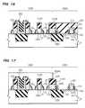
- a film-shaped first protective insulating layer 280is formed of silicon nitride or the like over the entire surface of the memory region 1000 and the logic circuit region 2000 , as shown in FIG. 7.
- a second protective insulating layer 290is formed of silicon oxide, silicon nitride oxide or the like, as shown in FIG. 8 .
- the second protective insulating layer 290 and the first protective insulating layer 280are polished using a CMP process so that the stopper layer S 100 is exposed, as shown in FIG. 9 .
- this stepcauses the first and second protective insulating layers 280 and 290 to be layered on the semiconductor substrate 10 on which the gate electrode 142 , the sidewall insulating layer 152 , and the like are formed.
- the gate layer 140is covered with the stopper layer S 100 .
- a resist layer (not shown) with a specific patternis formed.
- the gate layer 140 in the memory region 1000is patterned using the resist layer as a mask, thereby forming a word gate layers 140 a , as shown in FIG. 10 .
- openings 160 and 180are formed in a laminate consisting of the gate layer 140 and the stopper layer S 100 in the memory region 1000 as shown in a plan view in FIG. 11, whereby the word gate layer 140 a and the stopper layer S 100 are patterned. No opening is formed in the logic circuit region 2000 .
- the openings 160 and 180approximately correspond to regions in which the impurity layers are formed by ion implantation in a step described later.
- the side insulating layers and the control gatesare formed along the sides of the openings 160 and 180 in a step described later.
- the boundary section 140 b formed of the same material as the gate layer 140 and the stopper layer S 100 on the boundary section 140 bare formed on the element isolation region 300 at the boundary between the memory region 1000 and the logic circuit region 2000 , as shown in FIG. 10 .
- An ONO film 220is formed over the entire surface of the memory region 1000 and the logic circuit region 2000 , as shown in FIG. 12 .
- the ONO film 220is formed by depositing a first silicon oxide layer, a silicon nitride layer, and a second silicon oxide layer in that order.
- the first silicon oxide layermay be deposited using a thermal oxidation process, a CVD process, or the like.
- the silicon nitride layermay be deposited using, for example, a CVD process.
- the second silicon oxide layermay be deposited using a CVD process such as a high temperature oxidation (HTO) process. It is desirable to anneal these deposited layers, thereby causing each layer to be densified.
- HTOhigh temperature oxidation
- the ONO film 220 formed of the first silicon oxide layer, the silicon nitride layer and the second silicon oxide layeris patterned in a step described later, thereby forming the second gate insulating layer 22 and the side insulating layers 24 for the control gates 20 and 30 and the second contact insulating layer 210 , as shown in FIG. 3 .
- a doped polysilicon layer 230is formed over the entire surface of the ONO film 220 , as shown in FIG. 13.
- a first resist layer R 100is formed in a region in which the common contact section is formed.
- the entire surface of the doped polysilicon layer 230is anisotropically etched, thereby forming the conductive layers 40 (see FIG. 1) which form the first and second control gates 20 and 30 and the second contact conductive layer 232 (see FIG. 3 ), as shown in FIG. 14 .
- the control gates 20 and 30 in the shape of sidewallsare formed on the second gate insulating layer 22 along the sides of the openings 160 and 180 (see FIG. 11) in the memory region 1000 with the side insulating layers 24 interposed therebetween.
- the control gates 20 and 30are formed so that the upper ends thereof are located at a position lower than the upper surface of the word gate layer 140 a .
- the second contact conductive layer 232 for the common contact sections continuous with the control gates 20 and 30is formed in the areas masked by the first resist layers R 100 during this step.
- the first resist layer R 100is then removed.
- An insulating layer 250such as silicon oxide or silicon nitride oxide is formed over the entire surface of the memory region 1000 and the logic circuit region 2000 , as shown in FIG. 15 .
- the entire surface of the insulating layer 250(see FIG. 15) is anisotropically etched, whereby the insulating layers 25 are formed on the first and second control gates 20 and 30 , and the third contact insulating layer 252 is formed on the second contact conductive layer 232 in the memory region 1000 , as shown in FIG. 16 .
- the logic circuit region 2000is covered with at least the first and second protective insulating layers 280 and 290 .
- the second protective insulating layer 290(see FIG. 16) is removed in the logic circuit region 2000 by etching, as shown in FIG. 17 .
- the second resist layer R 200is formed so that the end on the side of the logic circuit region 2000 is located over the boundary section 140 b .
- the second protective insulating layer 290can be removed completely by forming the second resist layer R 200 in this manner.
- the second resist layer R 200is then removed.
- the first protective insulating layer 280(see FIG. 17) is removed in the logic circuit region 2000 , as shown in FIG. 18 .
- the third resist layer R 300is formed so that the end in the logic circuit region 2000 is located on the element isolation region 300 at an interval from the boundary section 140 b .
- the reason for forming the third resist layer R 300 in this manneris as follows: When the first protective insulating layer 280 is formed of silicon nitride, the first protective insulating layer 280 can be removed by thermal phosphoric acid.
- the third resist layer R 300is formed to cover the stopper layers S 100 on the boundary section 140 b so that the stopper layer S 100 in the boundary region between the memory region 1000 and the logic circuit region 2000 is not removed when removing the first protective insulating layer 280 . The third resist layer R 300 is then removed.
- the impurity layers 16 and 18 which form either the source region or drain region in the memory region 1000 and the impurity layers 162 and 182 which form either the source region or drain region in the logic circuit region 2000are formed in the semiconductor substrate 10 by ion implantation of impurities such as N-type impurities into the entire surface, as shown in FIG. 19 .
- Silicide layers 92 , 192 and 194such as a titanium silicide layer or cobalt silicide layer can be formed on the exposed areas of the impurity layers 16 , 18 , 162 and 182 and the upper surface of the gate electrode 142 by a conventional method.
- the MOS transistor 500is formed in this manner. No silicide layer is formed on the control gates 20 and 30 , since the insulating layers 25 are formed on the surfaces of the control gates 20 and 30 .
- the insulating layer 270(see FIG. 20) formed of silicon oxide, silicon nitride oxide or the like is formed over the entire surface of the memory region 1000 and the logic circuit region 2000 .
- the insulating layer 270is formed to cover the stopper layers S 100 .
- the insulating layer 270is polished using a CMP process so that the stopper layers S 100 are exposed, whereby the insulating layer 270 is planarized, as shown in FIG. 20 .
- the MOS transistor 500is covered with the insulating layer 270 in the logic circuit region 2000 .
- the buried insulating layer 70is formed between the opposing side insulating layers 24 with the control gates 20 and 30 interposed therebetween. This step causes the first and second control gates 20 and 30 to be completely covered with the buried insulating layer 70 and exposes the second conductive layer 232 .
- the stopper layers S 100are removed using thermal phosphoric acid, as shown in FIG. 21.
- a conductive layeris formed of a doped polysilicon layer in the memory region 1000 and the logic circuit region 2000 .
- a patterned resist layers R 400are formed on the doped polysilicon layer.
- the doped polysilicon layeris patterned using the resist layers R 400 as a mask, thereby forming the word lines 50 and the third contact conductive layers 260 .
- the word gate layer 140 a(see FIG. 20) is etched using the resist layers R 400 as a mask.
- the word gate layer 140 ais removed by this etching in the regions in which the word lines 50 are not formed.
- the word gates 14 arranged in an arraycan be formed.
- the regions in which the word gate layer 140 a is removedcorrespond to the regions in which the P-type impurity layers (element isolation impurity layers) 15 (see FIG. 2) are formed later.
- the conductive layers 40 which form the first and second control gates 20 and 30remain without being etched since the conductive layers 40 are covered with the buried insulating layers 70 .
- the MOS transistor 500 in the logic circuit region 2000is not affected by this etching since the MOS transistor 500 is completely covered with the insulating layer 270 .
- the entire surface of the semiconductor substrate 10is doped with P-type impurities. This causes the P-type impurity layers (element isolation impurity layers) 15 (see FIG. 2) to be formed in the regions between the word gates 14 adjacent in the Y direction.
- the elements of the nonvolatile semiconductor memory device 100can be isolated from one another more reliably by the P-type impurity layers 15 .
- contact holesare formed by a conventional method.
- Conductive layers and interconnect layerscan be formed in the contact holes.
- the conductive layer 82 and the interconnect layer 80 connected to the common contact section 200are formed, as shown in FIG. 3 .
- Contact sections and interconnect layerscan also be formed in the logic circuit region 2000 during this step.
- the semiconductor device shown in FIGS. 1 to 3can be fabricated by these steps.
- ion implantation steps for forming the source/drain regions 16 and 18 of the memory cells 100 and the source/drain regions 162 and 182 of the MOS transistors 500can be performed at the same time in the step (12).
- steps for self-alignably forming the silicide layers on the source/drain regions 16 and 18 of the memory cells 100 and the gate electrodes 142 and the source/drain regions 162 and 182 of the MOS transistors 500can be performed at the same time in the step (12).
- the source/drain regions 16 and 18 of the memory cells 100 and the source/drain regions 162 and 182 of the MOS transistors 500can be formed in a comparatively later step, highly controlled impurity layers can be formed without being affected by the earlier thermal treatment.
- a bulk semiconductor substrateis used as a semiconductor layer in the above embodiment.
- a semiconductor layer of an SOI substratemay be used.
Landscapes
- Non-Volatile Memory (AREA)
- Semiconductor Memories (AREA)
Abstract
Description
Claims (4)
Priority Applications (1)
| Application Number | Priority Date | Filing Date | Title |
|---|---|---|---|
| US09/953,856US6413821B1 (en) | 2001-09-18 | 2001-09-18 | Method of fabricating semiconductor device including nonvolatile memory and peripheral circuit |
Applications Claiming Priority (1)
| Application Number | Priority Date | Filing Date | Title |
|---|---|---|---|
| US09/953,856US6413821B1 (en) | 2001-09-18 | 2001-09-18 | Method of fabricating semiconductor device including nonvolatile memory and peripheral circuit |
Publications (1)
| Publication Number | Publication Date |
|---|---|
| US6413821B1true US6413821B1 (en) | 2002-07-02 |
Family
ID=25494620
Family Applications (1)
| Application Number | Title | Priority Date | Filing Date |
|---|---|---|---|
| US09/953,856Expired - Fee RelatedUS6413821B1 (en) | 2001-09-18 | 2001-09-18 | Method of fabricating semiconductor device including nonvolatile memory and peripheral circuit |
Country Status (1)
| Country | Link |
|---|---|
| US (1) | US6413821B1 (en) |
Cited By (47)
| Publication number | Priority date | Publication date | Assignee | Title |
|---|---|---|---|---|
| US6518124B1 (en)* | 2001-09-18 | 2003-02-11 | Seiko Epson Corporation | Method of fabricating semiconductor device |
| US20030058705A1 (en)* | 2001-09-25 | 2003-03-27 | Seiko Epson Corporation | Semiconductor device and method of manufacturing the same |
| US20030057505A1 (en)* | 2001-09-25 | 2003-03-27 | Seiko Epson Corporation | Semiconductor device and method of manufacturing the same |
| US20030067032A1 (en)* | 2001-10-08 | 2003-04-10 | Stmicroelectronics S.R.I. | Process for manufacturing a dual charge storage location memory cell |
| US20030082871A1 (en)* | 2001-10-31 | 2003-05-01 | Eliyahou Harari | Multi-state non-volatile integrated circuit memory systems that employ dielectric storage elements |
| US20030109093A1 (en)* | 2001-10-31 | 2003-06-12 | Eliyahou Harari | Multi-state non-volatile integrated circuit memory systems that employ dielectric storage elements |
| US20030157767A1 (en)* | 2002-02-20 | 2003-08-21 | Seiko Epson Corporation | Method of manufacturing semiconductor device |
| US20030166321A1 (en)* | 2002-02-20 | 2003-09-04 | Seiko Epson Corporation | Method of manufacturing semiconductor device |
| US20030181000A1 (en)* | 2002-03-05 | 2003-09-25 | Katsumi Mori | Method for fabricating nonvolatile memory device and method for fabricating semiconductor device |
| US6627491B2 (en) | 2001-09-14 | 2003-09-30 | Seiko Epson Corporation | Method of manufacturing non volatile memory device having two charge storage regions |
| US20030190805A1 (en)* | 2002-01-24 | 2003-10-09 | Seiko Epson Corporation | Method of manufacturing semiconductor device |
| US20030194841A1 (en)* | 2002-03-06 | 2003-10-16 | Susumu Inoue | Method for manufacturing semiconductor device |
| US20030219944A1 (en)* | 2002-03-01 | 2003-11-27 | Aiko Kato | Method for manufacturing a nonvolatile memory device |
| US20030218205A1 (en)* | 2002-03-22 | 2003-11-27 | Takashi Takamura | Nonvolatile memory device |
| US6664155B2 (en) | 2002-02-20 | 2003-12-16 | Seiko Epson Corporation | Method of manufacturing semiconductor device with memory area and logic circuit area |
| US20030235952A1 (en)* | 2002-02-22 | 2003-12-25 | Takumi Shibata | Method for manufacturing non-volatile memory device |
| US20040005761A1 (en)* | 2002-02-15 | 2004-01-08 | Takumi Shibata | Method for manufacturing non-volatile memory device |
| US20040018685A1 (en)* | 2002-03-05 | 2004-01-29 | Takumi Shibata | Method for manufacturing a nonvolatile memory device |
| US6706579B2 (en) | 2002-02-20 | 2004-03-16 | Seiko Epson Corporation | Method of manufacturing semiconductor device |
| US6709922B2 (en)* | 2001-01-30 | 2004-03-23 | Seiko Epson Corporation | Method of manufacturing semiconductor integrated circuit device including nonvolatile semiconductor memory devices |
| US20040072403A1 (en)* | 2002-09-11 | 2004-04-15 | Seiko Epson Corporation | Method of manufacturing semiconductor device |
| US20040072402A1 (en)* | 2002-09-02 | 2004-04-15 | Seiko Epson Corporation | Semiconductor device and method of fabricating the same |
| US20040077145A1 (en)* | 2002-07-12 | 2004-04-22 | Seiko Epson Corporation | Method of fabricating semiconductor device |
| US20040097035A1 (en)* | 2002-09-18 | 2004-05-20 | Seiko Epson Corporation | Method of manufacturing semiconductor device |
| US20040108535A1 (en)* | 2000-06-16 | 2004-06-10 | Drynan John M. | Interconnect line selectively isolated from an underlying contact plug |
| US20040129972A1 (en)* | 2002-10-30 | 2004-07-08 | Seiko Epson Corporation | Semiconductor device and method of manufacturing the same |
| US20040132247A1 (en)* | 2002-10-30 | 2004-07-08 | Seiko Epson Corporation | Semiconductor device and method of manufacturing the same |
| US20040135196A1 (en)* | 2002-10-24 | 2004-07-15 | Seiko Epson Corporation | Semiconductor device and method of manufacturing the same |
| US20040135192A1 (en)* | 2002-10-29 | 2004-07-15 | Seiko Epson Corporation | Semiconductor device and method of manufacturing the same |
| US6818507B2 (en) | 2002-01-23 | 2004-11-16 | Seiko Epson Corporation | Method of manufacturing semiconductor device including memory region and logic circuit region |
| US6828199B2 (en)* | 2001-12-20 | 2004-12-07 | Advanced Micro Devices, Ltd. | Monos device having buried metal silicide bit line |
| US20050029574A1 (en)* | 2003-08-08 | 2005-02-10 | Hee-Seog Jeon | Self-aligned 1 bit local SONOS memory cell and method of fabricating the same |
| US6900098B1 (en)* | 2002-10-15 | 2005-05-31 | Halo Lsi, Inc. | Twin insulator charge storage device operation and its fabrication method |
| US20050251617A1 (en)* | 2004-05-07 | 2005-11-10 | Sinclair Alan W | Hybrid non-volatile memory system |
| US20050275008A1 (en)* | 2004-06-14 | 2005-12-15 | Erh-Kun Lai | [non-volatile memory and fabrication thereof] |
| US6995420B2 (en) | 2001-09-25 | 2006-02-07 | Seiko Epson Corporation | Semiconductor device and method of manufacturing the same |
| US20060170030A1 (en)* | 2005-02-03 | 2006-08-03 | Seiko Epson Corporation | Semiconductor device |
| US20060244014A1 (en)* | 2003-01-22 | 2006-11-02 | Samsung Electronics Co., Ltd. | Nonvolatile memory device and method of forming same |
| CN1310330C (en)* | 2002-07-10 | 2007-04-11 | 株式会社东芝 | Semiconductor memory device with recording area and periphery area and manufacture thereof |
| CN1312762C (en)* | 2003-07-25 | 2007-04-25 | 旺宏电子股份有限公司 | Method for forming non-volatile memory cells and semiconductor structures formed by this method |
| US20070201272A1 (en)* | 2004-08-09 | 2007-08-30 | Tsutomu Okazaki | Semiconductor device |
| CN1976041B (en)* | 2005-12-02 | 2010-12-01 | 冲电气工业株式会社 | Nonvolatile semiconductor memory device and manufacturing method thereof |
| US20110024820A1 (en)* | 2004-06-30 | 2011-02-03 | Takeshi Sakai | Method of manufacturing a nonvolatile semiconductor memory device, and a nonvolatile semiconductor memory device |
| US20150048433A1 (en)* | 2013-08-16 | 2015-02-19 | Taiwan Semiconductor Manufacturing Company, Ltd. | Contact Formation for Split Gate Flash Memory |
| CN105374753A (en)* | 2014-07-07 | 2016-03-02 | 中芯国际集成电路制造(上海)有限公司 | Manufacture method of memory |
| CN107946312A (en)* | 2017-11-23 | 2018-04-20 | 长江存储科技有限责任公司 | Method and structure for preventing peripheral circuits from being damaged |
| US10756113B2 (en) | 2017-11-23 | 2020-08-25 | Yangtze Memory Technologies Co., Ltd. | Protective structure and fabrication methods for the peripheral circuits of a three-dimensional memory |
Citations (7)
| Publication number | Priority date | Publication date | Assignee | Title |
|---|---|---|---|---|
| US5408115A (en) | 1994-04-04 | 1995-04-18 | Motorola Inc. | Self-aligned, split-gate EEPROM device |
| US5422504A (en) | 1994-05-02 | 1995-06-06 | Motorola Inc. | EEPROM memory device having a sidewall spacer floating gate electrode and process |
| US5917218A (en)* | 1996-02-21 | 1999-06-29 | Samsung Electronics Co., Ltd. | Peripheral circuits including high voltage transistors with LDD structures for nonvolatile memories |
| US5969383A (en) | 1997-06-16 | 1999-10-19 | Motorola, Inc. | Split-gate memory device and method for accessing the same |
| US6177318B1 (en) | 1999-10-18 | 2001-01-23 | Halo Lsi Design & Device Technology, Inc. | Integration method for sidewall split gate monos transistor |
| US6248633B1 (en) | 1999-10-25 | 2001-06-19 | Halo Lsi Design & Device Technology, Inc. | Process for making and programming and operating a dual-bit multi-level ballistic MONOS memory |
| US6255166B1 (en) | 1999-08-05 | 2001-07-03 | Aalo Lsi Design & Device Technology, Inc. | Nonvolatile memory cell, method of programming the same and nonvolatile memory array |
- 2001
- 2001-09-18USUS09/953,856patent/US6413821B1/ennot_activeExpired - Fee Related
Patent Citations (8)
| Publication number | Priority date | Publication date | Assignee | Title |
|---|---|---|---|---|
| US5408115A (en) | 1994-04-04 | 1995-04-18 | Motorola Inc. | Self-aligned, split-gate EEPROM device |
| US5422504A (en) | 1994-05-02 | 1995-06-06 | Motorola Inc. | EEPROM memory device having a sidewall spacer floating gate electrode and process |
| US5494838A (en) | 1994-05-02 | 1996-02-27 | Motorola, Inc. | Process of making EEPROM memory device having a sidewall spacer floating gate electrode |
| US5917218A (en)* | 1996-02-21 | 1999-06-29 | Samsung Electronics Co., Ltd. | Peripheral circuits including high voltage transistors with LDD structures for nonvolatile memories |
| US5969383A (en) | 1997-06-16 | 1999-10-19 | Motorola, Inc. | Split-gate memory device and method for accessing the same |
| US6255166B1 (en) | 1999-08-05 | 2001-07-03 | Aalo Lsi Design & Device Technology, Inc. | Nonvolatile memory cell, method of programming the same and nonvolatile memory array |
| US6177318B1 (en) | 1999-10-18 | 2001-01-23 | Halo Lsi Design & Device Technology, Inc. | Integration method for sidewall split gate monos transistor |
| US6248633B1 (en) | 1999-10-25 | 2001-06-19 | Halo Lsi Design & Device Technology, Inc. | Process for making and programming and operating a dual-bit multi-level ballistic MONOS memory |
Non-Patent Citations (4)
| Title |
|---|
| 09/953,855 Sep. 18, 2001. |
| Chang, Kuo-Tung et al., "A New SONOS Memory Using Source-Side Injection for Programming", 1998 IEEE Electron Device Letters, vol. 19, No. 7, Jul. 1998, pp. 253-255. |
| Chen, Wei-Ming et al., "A Novel Flash Memory Device with SPlit Gate Source Side Injection and ONO Charge Storage Stack (SPIN)", 1997 Symposium on VLSI Technology Digest of Technical Papers, pp. 63-64. |
| Hayashi, Yutaka et al., "Twin MONOS Cell with Dual Control Gates", 2000 IEEE Symposium on VLSI Technology Digest of Technical Papers. |
Cited By (104)
| Publication number | Priority date | Publication date | Assignee | Title |
|---|---|---|---|---|
| US20040108535A1 (en)* | 2000-06-16 | 2004-06-10 | Drynan John M. | Interconnect line selectively isolated from an underlying contact plug |
| US7061115B2 (en)* | 2000-06-16 | 2006-06-13 | Micron Technology, Inc. | Interconnect line selectively isolated from an underlying contact plug |
| US6709922B2 (en)* | 2001-01-30 | 2004-03-23 | Seiko Epson Corporation | Method of manufacturing semiconductor integrated circuit device including nonvolatile semiconductor memory devices |
| US6627491B2 (en) | 2001-09-14 | 2003-09-30 | Seiko Epson Corporation | Method of manufacturing non volatile memory device having two charge storage regions |
| US6518124B1 (en)* | 2001-09-18 | 2003-02-11 | Seiko Epson Corporation | Method of fabricating semiconductor device |
| US6891271B2 (en) | 2001-09-25 | 2005-05-10 | Seiko Epson Corporation | Non-volatile memory device |
| US6995420B2 (en) | 2001-09-25 | 2006-02-07 | Seiko Epson Corporation | Semiconductor device and method of manufacturing the same |
| US7005328B2 (en) | 2001-09-25 | 2006-02-28 | Seiko Epson Corporation | Non-volatile memory device |
| US20050032312A1 (en)* | 2001-09-25 | 2005-02-10 | Seiko Epson Corporation | Non-volatile memory device |
| US6812520B2 (en) | 2001-09-25 | 2004-11-02 | Seiko Epson Corporation | Semiconductor device and method of manufacturing the same |
| US20030057505A1 (en)* | 2001-09-25 | 2003-03-27 | Seiko Epson Corporation | Semiconductor device and method of manufacturing the same |
| US20030058705A1 (en)* | 2001-09-25 | 2003-03-27 | Seiko Epson Corporation | Semiconductor device and method of manufacturing the same |
| US7115472B2 (en) | 2001-10-08 | 2006-10-03 | Stmicroelectronics, S.R.L. | Process for manufacturing a dual charge storage location memory cell |
| US20030067032A1 (en)* | 2001-10-08 | 2003-04-10 | Stmicroelectronics S.R.I. | Process for manufacturing a dual charge storage location memory cell |
| US20050064654A1 (en)* | 2001-10-08 | 2005-03-24 | Stmicroelectronics S.R.L | Process for manufacturing a dual charge storage location memory cell |
| US6825523B2 (en)* | 2001-10-08 | 2004-11-30 | Stmicroelectronics S.R.L. | Process for manufacturing a dual charge storage location memory cell |
| US6925007B2 (en) | 2001-10-31 | 2005-08-02 | Sandisk Corporation | Multi-state non-volatile integrated circuit memory systems that employ dielectric storage elements |
| US20080119026A1 (en)* | 2001-10-31 | 2008-05-22 | Eliyahou Harari | Multi-State Non-Volatile Integrated Circuit Memory Systems that Employ Dielectric Storage Elements |
| US20050157551A1 (en)* | 2001-10-31 | 2005-07-21 | Eliyahou Harari | Multi-state non-volatile integrated circuit memory systems that employ dielectric storage elements |
| US6897522B2 (en) | 2001-10-31 | 2005-05-24 | Sandisk Corporation | Multi-state non-volatile integrated circuit memory systems that employ dielectric storage elements |
| US7479677B2 (en) | 2001-10-31 | 2009-01-20 | Sandisk Corporation | Multi-state non-volatile integrated circuit memory systems that employ dielectric storage elements |
| US7341918B2 (en) | 2001-10-31 | 2008-03-11 | Sandisk Corporation | Multi-state non-volatile integrated circuit memory systems that employ dielectric storage elements |
| US20030082871A1 (en)* | 2001-10-31 | 2003-05-01 | Eliyahou Harari | Multi-state non-volatile integrated circuit memory systems that employ dielectric storage elements |
| US20030109093A1 (en)* | 2001-10-31 | 2003-06-12 | Eliyahou Harari | Multi-state non-volatile integrated circuit memory systems that employ dielectric storage elements |
| US20050180210A1 (en)* | 2001-10-31 | 2005-08-18 | Eliyahou Harari | Multi-state non-volatile integrated circuit memory systems that employ dielectric storage elements |
| US7579247B2 (en) | 2001-10-31 | 2009-08-25 | Sandisk Corporation | Multi-state non-volatile integrated circuit memory systems that employ dielectric storage elements |
| US20080116509A1 (en)* | 2001-10-31 | 2008-05-22 | Eliyahou Harari | Multi-State Non-Volatile Integrated Circuit Memory Systems that Employ Dielectric Storage Elements |
| US7834392B2 (en) | 2001-10-31 | 2010-11-16 | Sandisk Corporation | Multi-state non-volatile integrated circuit memory systems that employ dielectric storage elements |
| US7342279B2 (en) | 2001-10-31 | 2008-03-11 | Sandisk Corporation | Multi-state non-volatile integrated circuit memory systems that employ dielectric storage elements |
| US6828199B2 (en)* | 2001-12-20 | 2004-12-07 | Advanced Micro Devices, Ltd. | Monos device having buried metal silicide bit line |
| US6818507B2 (en) | 2002-01-23 | 2004-11-16 | Seiko Epson Corporation | Method of manufacturing semiconductor device including memory region and logic circuit region |
| US20030190805A1 (en)* | 2002-01-24 | 2003-10-09 | Seiko Epson Corporation | Method of manufacturing semiconductor device |
| US6849553B2 (en)* | 2002-01-24 | 2005-02-01 | Seiko Epson Corporation | Method of manufacturing semiconductor device |
| US20040005761A1 (en)* | 2002-02-15 | 2004-01-08 | Takumi Shibata | Method for manufacturing non-volatile memory device |
| US6812097B2 (en)* | 2002-02-15 | 2004-11-02 | Seiko Epson Corporation | Method for manufacturing non-volatile memory device |
| US20030166321A1 (en)* | 2002-02-20 | 2003-09-04 | Seiko Epson Corporation | Method of manufacturing semiconductor device |
| US6815291B2 (en) | 2002-02-20 | 2004-11-09 | Seiko Epson Corporation | Method of manufacturing semiconductor device |
| US6664155B2 (en) | 2002-02-20 | 2003-12-16 | Seiko Epson Corporation | Method of manufacturing semiconductor device with memory area and logic circuit area |
| US20030157767A1 (en)* | 2002-02-20 | 2003-08-21 | Seiko Epson Corporation | Method of manufacturing semiconductor device |
| US6930000B2 (en) | 2002-02-20 | 2005-08-16 | Seiko Epson Corporation | Method of manufacturing semiconductor device |
| US6706579B2 (en) | 2002-02-20 | 2004-03-16 | Seiko Epson Corporation | Method of manufacturing semiconductor device |
| US20030235952A1 (en)* | 2002-02-22 | 2003-12-25 | Takumi Shibata | Method for manufacturing non-volatile memory device |
| US20030219944A1 (en)* | 2002-03-01 | 2003-11-27 | Aiko Kato | Method for manufacturing a nonvolatile memory device |
| US6849500B2 (en)* | 2002-03-01 | 2005-02-01 | Seiko Epson Corporation | Method for manufacturing a nonvolatile memory device including an opening formed into an inverse-tapered shape |
| US20040018685A1 (en)* | 2002-03-05 | 2004-01-29 | Takumi Shibata | Method for manufacturing a nonvolatile memory device |
| US7087487B2 (en)* | 2002-03-05 | 2006-08-08 | Seiko Epson Corporation | Method for fabricating nonvolatile memory device and method for fabricating semiconductor device |
| US6943082B2 (en) | 2002-03-05 | 2005-09-13 | Seiko Epson Corporation | Method for manufacturing a nonvolatile memory device |
| US20030181000A1 (en)* | 2002-03-05 | 2003-09-25 | Katsumi Mori | Method for fabricating nonvolatile memory device and method for fabricating semiconductor device |
| US20030194841A1 (en)* | 2002-03-06 | 2003-10-16 | Susumu Inoue | Method for manufacturing semiconductor device |
| US6737322B2 (en) | 2002-03-06 | 2004-05-18 | Seiko Epson Corporation | Method for manufacturing semiconductor device |
| US20030218205A1 (en)* | 2002-03-22 | 2003-11-27 | Takashi Takamura | Nonvolatile memory device |
| US6809374B2 (en) | 2002-03-22 | 2004-10-26 | Seiko Epson Corporation | Nonvolatile memory device |
| CN1310330C (en)* | 2002-07-10 | 2007-04-11 | 株式会社东芝 | Semiconductor memory device with recording area and periphery area and manufacture thereof |
| US20040077145A1 (en)* | 2002-07-12 | 2004-04-22 | Seiko Epson Corporation | Method of fabricating semiconductor device |
| US6787417B2 (en) | 2002-07-12 | 2004-09-07 | Seiko Epson Corporation | Method of fabricating semiconductor device |
| US6972456B2 (en) | 2002-09-02 | 2005-12-06 | Seiko Epson Corporation | Semiconductor device and method of fabricating the same |
| US20040072402A1 (en)* | 2002-09-02 | 2004-04-15 | Seiko Epson Corporation | Semiconductor device and method of fabricating the same |
| US6989305B2 (en) | 2002-09-11 | 2006-01-24 | Seiko Epson Corporation | Method of manufacturing semiconductor device |
| US20040072403A1 (en)* | 2002-09-11 | 2004-04-15 | Seiko Epson Corporation | Method of manufacturing semiconductor device |
| US20040097035A1 (en)* | 2002-09-18 | 2004-05-20 | Seiko Epson Corporation | Method of manufacturing semiconductor device |
| US6930003B2 (en) | 2002-09-18 | 2005-08-16 | Seiko Epson Corporation | Method of manufacturing semiconductor device |
| US6900098B1 (en)* | 2002-10-15 | 2005-05-31 | Halo Lsi, Inc. | Twin insulator charge storage device operation and its fabrication method |
| US20040135196A1 (en)* | 2002-10-24 | 2004-07-15 | Seiko Epson Corporation | Semiconductor device and method of manufacturing the same |
| US20040135192A1 (en)* | 2002-10-29 | 2004-07-15 | Seiko Epson Corporation | Semiconductor device and method of manufacturing the same |
| US7015542B2 (en) | 2002-10-29 | 2006-03-21 | Seiko Epson Corporation | MONOS memory device |
| US20040129972A1 (en)* | 2002-10-30 | 2004-07-08 | Seiko Epson Corporation | Semiconductor device and method of manufacturing the same |
| US6953967B2 (en) | 2002-10-30 | 2005-10-11 | Seiko Epson Corporation | Semiconductor device and method of manufacturing the same |
| US20040132247A1 (en)* | 2002-10-30 | 2004-07-08 | Seiko Epson Corporation | Semiconductor device and method of manufacturing the same |
| US6798015B2 (en) | 2002-10-30 | 2004-09-28 | Seiko Epson Corporation | Semiconductor device and method of manufacturing the same |
| US20060244014A1 (en)* | 2003-01-22 | 2006-11-02 | Samsung Electronics Co., Ltd. | Nonvolatile memory device and method of forming same |
| CN1312762C (en)* | 2003-07-25 | 2007-04-25 | 旺宏电子股份有限公司 | Method for forming non-volatile memory cells and semiconductor structures formed by this method |
| US7768061B2 (en) | 2003-08-08 | 2010-08-03 | Samsung Electronics Co., Ltd. | Self aligned 1 bit local SONOS memory cell |
| US20050029574A1 (en)* | 2003-08-08 | 2005-02-10 | Hee-Seog Jeon | Self-aligned 1 bit local SONOS memory cell and method of fabricating the same |
| US7141473B2 (en) | 2003-08-08 | 2006-11-28 | Samsung Electronics Co., Ltd. | Self-aligned 1 bit local SONOS memory cell and method of fabricating the same |
| US20070063267A1 (en)* | 2003-08-08 | 2007-03-22 | Samsung Electronics Co., Ltd. | Self aligned 1 bit local SONOS memory cell |
| DE102004038874B4 (en)* | 2003-08-08 | 2006-09-28 | Samsung Electronics Co., Ltd. | 1-bit SONOS memory cell and manufacturing process |
| US20100023681A1 (en)* | 2004-05-07 | 2010-01-28 | Alan Welsh Sinclair | Hybrid Non-Volatile Memory System |
| US20050251617A1 (en)* | 2004-05-07 | 2005-11-10 | Sinclair Alan W | Hybrid non-volatile memory system |
| US20050275008A1 (en)* | 2004-06-14 | 2005-12-15 | Erh-Kun Lai | [non-volatile memory and fabrication thereof] |
| US8390048B2 (en)* | 2004-06-30 | 2013-03-05 | Renesas Electronics Corporation | Method of manufacturing a nonvolatile semiconductor memory device, and a nonvolatile semiconductor memory device |
| US20110024820A1 (en)* | 2004-06-30 | 2011-02-03 | Takeshi Sakai | Method of manufacturing a nonvolatile semiconductor memory device, and a nonvolatile semiconductor memory device |
| US8319265B2 (en) | 2004-08-09 | 2012-11-27 | Renesas Electronics Corporation | Semiconductor device with improved common source arrangement for adjacent non-volatile memory cells |
| US9640546B2 (en) | 2004-08-09 | 2017-05-02 | Renesas Electronics Corporation | Semiconductor device |
| US20100038700A1 (en)* | 2004-08-09 | 2010-02-18 | Tsutomu Okazaki | Semiconductor Device |
| US20090122609A1 (en)* | 2004-08-09 | 2009-05-14 | Tsutomu Okazaki | Semiconductor device |
| US7502257B2 (en)* | 2004-08-09 | 2009-03-10 | Renesas Technology Corp. | Semiconductor device |
| US10910394B2 (en) | 2004-08-09 | 2021-02-02 | Renesas Electronics Corporation | Semiconductor device |
| US7636253B2 (en) | 2004-08-09 | 2009-12-22 | Renesas Technology Corp. | Semiconductor device |
| US10692878B2 (en) | 2004-08-09 | 2020-06-23 | Renesas Electronics Corporation | Semiconductor device |
| US20070201272A1 (en)* | 2004-08-09 | 2007-08-30 | Tsutomu Okazaki | Semiconductor device |
| US10396089B2 (en) | 2004-08-09 | 2019-08-27 | Renesas Electronics Corporation | Semiconductor device |
| US8963226B2 (en) | 2004-08-09 | 2015-02-24 | Renesas Electronics Corporation | Semiconductor device with gate electrodes |
| US10141324B2 (en) | 2004-08-09 | 2018-11-27 | Renesas Electronics Corporation | Semiconductor device |
| US7473962B2 (en)* | 2005-02-03 | 2009-01-06 | Seiko Epson Corporation | Semiconductor device having nonvolatile memory device with improved charge holding property |
| US20060170030A1 (en)* | 2005-02-03 | 2006-08-03 | Seiko Epson Corporation | Semiconductor device |
| CN1976041B (en)* | 2005-12-02 | 2010-12-01 | 冲电气工业株式会社 | Nonvolatile semiconductor memory device and manufacturing method thereof |
| US9390927B2 (en)* | 2013-08-16 | 2016-07-12 | Taiwan Semiconductor Manufacturing Company, Ltd. | Contact formation for split gate flash memory |
| US10068773B2 (en) | 2013-08-16 | 2018-09-04 | Taiwan Semiconductor Manufacturing Company, Ltd. | Contact formation for split gate flash memory |
| US20150048433A1 (en)* | 2013-08-16 | 2015-02-19 | Taiwan Semiconductor Manufacturing Company, Ltd. | Contact Formation for Split Gate Flash Memory |
| CN105374753A (en)* | 2014-07-07 | 2016-03-02 | 中芯国际集成电路制造(上海)有限公司 | Manufacture method of memory |
| CN105374753B (en)* | 2014-07-07 | 2019-07-05 | 中芯国际集成电路制造(上海)有限公司 | A kind of manufacturing method of memory |
| CN107946312A (en)* | 2017-11-23 | 2018-04-20 | 长江存储科技有限责任公司 | Method and structure for preventing peripheral circuits from being damaged |
| US10756113B2 (en) | 2017-11-23 | 2020-08-25 | Yangtze Memory Technologies Co., Ltd. | Protective structure and fabrication methods for the peripheral circuits of a three-dimensional memory |
| US11404442B2 (en) | 2017-11-23 | 2022-08-02 | Yangtze Memory Technologies Co., Ltd. | Protective structure and fabrication methods for the peripheral circuits of a three-dimensional memory |
Similar Documents
| Publication | Publication Date | Title |
|---|---|---|
| US6413821B1 (en) | Method of fabricating semiconductor device including nonvolatile memory and peripheral circuit | |
| US7005328B2 (en) | Non-volatile memory device | |
| US6518124B1 (en) | Method of fabricating semiconductor device | |
| US6709922B2 (en) | Method of manufacturing semiconductor integrated circuit device including nonvolatile semiconductor memory devices | |
| US6627491B2 (en) | Method of manufacturing non volatile memory device having two charge storage regions | |
| US6720579B2 (en) | Semiconductor device and method of manufacturing the same | |
| US6809385B2 (en) | Semiconductor integrated circuit device including nonvolatile semiconductor memory devices having control gates connected to common contact section | |
| US6995420B2 (en) | Semiconductor device and method of manufacturing the same | |
| JP3726760B2 (en) | Manufacturing method of semiconductor device | |
| US6812520B2 (en) | Semiconductor device and method of manufacturing the same | |
| US6818507B2 (en) | Method of manufacturing semiconductor device including memory region and logic circuit region | |
| US6737322B2 (en) | Method for manufacturing semiconductor device | |
| US6656794B2 (en) | Method of manufacturing semiconductor device including a memory area and a logic circuit area | |
| KR20020050115A (en) | Semiconductor memory device with silicide layer formed selectively | |
| KR20020062590A (en) | Semiconductor memory device and manufacturing method thereof | |
| US20030219944A1 (en) | Method for manufacturing a nonvolatile memory device | |
| JP3622741B2 (en) | Manufacturing method of semiconductor device | |
| US7087487B2 (en) | Method for fabricating nonvolatile memory device and method for fabricating semiconductor device | |
| JP4300394B2 (en) | Manufacturing method of semiconductor device | |
| JP3675381B2 (en) | Manufacturing method of semiconductor device | |
| JP3653540B2 (en) | Manufacturing method of semiconductor device |
Legal Events
| Date | Code | Title | Description |
|---|---|---|---|
| AS | Assignment | Owner name:SEIKO EPSON CORPORATION, JAPAN Free format text:ASSIGNMENT OF ASSIGNORS INTEREST;ASSIGNORS:EBINA, AKIHIKO;INOUE, SUSUMU;REEL/FRAME:012591/0784 Effective date:20011204 Owner name:HALO LSI DESIGN & DEVICE TECHNOLOGY, INC., NEW YOR Free format text:ASSIGNMENT OF ASSIGNORS INTEREST;ASSIGNORS:EBINA, AKIHIKO;INOUE, SUSUMU;REEL/FRAME:012591/0784 Effective date:20011204 | |
| AS | Assignment | Owner name:SEIKO EPSON CORPORATION, JAPAN Free format text:ASSIGNMENT OF ASSIGNORS INTEREST;ASSIGNOR:HALO LSI DESIGN & DEVICE TECHNOLOGY, INC.;REEL/FRAME:013868/0603 Effective date:20030710 | |
| FEPP | Fee payment procedure | Free format text:PAYOR NUMBER ASSIGNED (ORIGINAL EVENT CODE: ASPN); ENTITY STATUS OF PATENT OWNER: LARGE ENTITY Free format text:PAYER NUMBER DE-ASSIGNED (ORIGINAL EVENT CODE: RMPN); ENTITY STATUS OF PATENT OWNER: LARGE ENTITY | |
| FPAY | Fee payment | Year of fee payment:4 | |
| REMI | Maintenance fee reminder mailed | ||
| LAPS | Lapse for failure to pay maintenance fees | ||
| STCH | Information on status: patent discontinuation | Free format text:PATENT EXPIRED DUE TO NONPAYMENT OF MAINTENANCE FEES UNDER 37 CFR 1.362 | |
| FP | Lapsed due to failure to pay maintenance fee | Effective date:20100702 |