US6411333B1 - Format conversion using patch-based filtering - Google Patents
Format conversion using patch-based filteringDownload PDFInfo
- Publication number
- US6411333B1 US6411333B1US09/285,490US28549099AUS6411333B1US 6411333 B1US6411333 B1US 6411333B1US 28549099 AUS28549099 AUS 28549099AUS 6411333 B1US6411333 B1US 6411333B1
- Authority
- US
- United States
- Prior art keywords
- image data
- buffer
- data
- memory
- filter
- Prior art date
- Legal status (The legal status is an assumption and is not a legal conclusion. Google has not performed a legal analysis and makes no representation as to the accuracy of the status listed.)
- Expired - Lifetime
Links
Images


Classifications
- G—PHYSICS
- G06—COMPUTING OR CALCULATING; COUNTING
- G06T—IMAGE DATA PROCESSING OR GENERATION, IN GENERAL
- G06T3/00—Geometric image transformations in the plane of the image
- G06T3/40—Scaling of whole images or parts thereof, e.g. expanding or contracting
- G—PHYSICS
- G09—EDUCATION; CRYPTOGRAPHY; DISPLAY; ADVERTISING; SEALS
- G09G—ARRANGEMENTS OR CIRCUITS FOR CONTROL OF INDICATING DEVICES USING STATIC MEANS TO PRESENT VARIABLE INFORMATION
- G09G5/00—Control arrangements or circuits for visual indicators common to cathode-ray tube indicators and other visual indicators
- G09G5/14—Display of multiple viewports
- G—PHYSICS
- G09—EDUCATION; CRYPTOGRAPHY; DISPLAY; ADVERTISING; SEALS
- G09G—ARRANGEMENTS OR CIRCUITS FOR CONTROL OF INDICATING DEVICES USING STATIC MEANS TO PRESENT VARIABLE INFORMATION
- G09G5/00—Control arrangements or circuits for visual indicators common to cathode-ray tube indicators and other visual indicators
- G09G5/36—Control arrangements or circuits for visual indicators common to cathode-ray tube indicators and other visual indicators characterised by the display of a graphic pattern, e.g. using an all-points-addressable [APA] memory
- G09G5/39—Control of the bit-mapped memory
- G09G5/393—Arrangements for updating the contents of the bit-mapped memory
- H—ELECTRICITY
- H04—ELECTRIC COMMUNICATION TECHNIQUE
- H04N—PICTORIAL COMMUNICATION, e.g. TELEVISION
- H04N21/00—Selective content distribution, e.g. interactive television or video on demand [VOD]
- H04N21/40—Client devices specifically adapted for the reception of or interaction with content, e.g. set-top-box [STB]; Operations thereof
- H04N21/41—Structure of client; Structure of client peripherals
- H04N21/426—Internal components of the client ; Characteristics thereof
- H—ELECTRICITY
- H04—ELECTRIC COMMUNICATION TECHNIQUE
- H04N—PICTORIAL COMMUNICATION, e.g. TELEVISION
- H04N21/00—Selective content distribution, e.g. interactive television or video on demand [VOD]
- H04N21/40—Client devices specifically adapted for the reception of or interaction with content, e.g. set-top-box [STB]; Operations thereof
- H04N21/43—Processing of content or additional data, e.g. demultiplexing additional data from a digital video stream; Elementary client operations, e.g. monitoring of home network or synchronising decoder's clock; Client middleware
- H04N21/431—Generation of visual interfaces for content selection or interaction; Content or additional data rendering
- H04N21/4312—Generation of visual interfaces for content selection or interaction; Content or additional data rendering involving specific graphical features, e.g. screen layout, special fonts or colors, blinking icons, highlights or animations
- H04N21/4316—Generation of visual interfaces for content selection or interaction; Content or additional data rendering involving specific graphical features, e.g. screen layout, special fonts or colors, blinking icons, highlights or animations for displaying supplemental content in a region of the screen, e.g. an advertisement in a separate window
- H—ELECTRICITY
- H04—ELECTRIC COMMUNICATION TECHNIQUE
- H04N—PICTORIAL COMMUNICATION, e.g. TELEVISION
- H04N21/00—Selective content distribution, e.g. interactive television or video on demand [VOD]
- H04N21/40—Client devices specifically adapted for the reception of or interaction with content, e.g. set-top-box [STB]; Operations thereof
- H04N21/43—Processing of content or additional data, e.g. demultiplexing additional data from a digital video stream; Elementary client operations, e.g. monitoring of home network or synchronising decoder's clock; Client middleware
- H04N21/44—Processing of video elementary streams, e.g. splicing a video clip retrieved from local storage with an incoming video stream or rendering scenes according to encoded video stream scene graphs
- H04N21/4402—Processing of video elementary streams, e.g. splicing a video clip retrieved from local storage with an incoming video stream or rendering scenes according to encoded video stream scene graphs involving reformatting operations of video signals for household redistribution, storage or real-time display
- H04N21/440218—Processing of video elementary streams, e.g. splicing a video clip retrieved from local storage with an incoming video stream or rendering scenes according to encoded video stream scene graphs involving reformatting operations of video signals for household redistribution, storage or real-time display by transcoding between formats or standards, e.g. from MPEG-2 to MPEG-4
- H—ELECTRICITY
- H04—ELECTRIC COMMUNICATION TECHNIQUE
- H04N—PICTORIAL COMMUNICATION, e.g. TELEVISION
- H04N21/00—Selective content distribution, e.g. interactive television or video on demand [VOD]
- H04N21/40—Client devices specifically adapted for the reception of or interaction with content, e.g. set-top-box [STB]; Operations thereof
- H04N21/43—Processing of content or additional data, e.g. demultiplexing additional data from a digital video stream; Elementary client operations, e.g. monitoring of home network or synchronising decoder's clock; Client middleware
- H04N21/44—Processing of video elementary streams, e.g. splicing a video clip retrieved from local storage with an incoming video stream or rendering scenes according to encoded video stream scene graphs
- H04N21/4402—Processing of video elementary streams, e.g. splicing a video clip retrieved from local storage with an incoming video stream or rendering scenes according to encoded video stream scene graphs involving reformatting operations of video signals for household redistribution, storage or real-time display
- H04N21/440263—Processing of video elementary streams, e.g. splicing a video clip retrieved from local storage with an incoming video stream or rendering scenes according to encoded video stream scene graphs involving reformatting operations of video signals for household redistribution, storage or real-time display by altering the spatial resolution, e.g. for displaying on a connected PDA
- H—ELECTRICITY
- H04—ELECTRIC COMMUNICATION TECHNIQUE
- H04N—PICTORIAL COMMUNICATION, e.g. TELEVISION
- H04N21/00—Selective content distribution, e.g. interactive television or video on demand [VOD]
- H04N21/40—Client devices specifically adapted for the reception of or interaction with content, e.g. set-top-box [STB]; Operations thereof
- H04N21/43—Processing of content or additional data, e.g. demultiplexing additional data from a digital video stream; Elementary client operations, e.g. monitoring of home network or synchronising decoder's clock; Client middleware
- H04N21/443—OS processes, e.g. booting an STB, implementing a Java virtual machine in an STB or power management in an STB
- H04N21/4435—Memory management
- H—ELECTRICITY
- H04—ELECTRIC COMMUNICATION TECHNIQUE
- H04N—PICTORIAL COMMUNICATION, e.g. TELEVISION
- H04N5/00—Details of television systems
- H04N5/44—Receiver circuitry for the reception of television signals according to analogue transmission standards
- H04N5/445—Receiver circuitry for the reception of television signals according to analogue transmission standards for displaying additional information
- H04N5/45—Picture in picture, e.g. displaying simultaneously another television channel in a region of the screen
- H—ELECTRICITY
- H04—ELECTRIC COMMUNICATION TECHNIQUE
- H04N—PICTORIAL COMMUNICATION, e.g. TELEVISION
- H04N5/00—Details of television systems
- H04N5/44—Receiver circuitry for the reception of television signals according to analogue transmission standards
- H04N5/46—Receiver circuitry for the reception of television signals according to analogue transmission standards for receiving on more than one standard at will
- H—ELECTRICITY
- H04—ELECTRIC COMMUNICATION TECHNIQUE
- H04N—PICTORIAL COMMUNICATION, e.g. TELEVISION
- H04N7/00—Television systems
- H04N7/01—Conversion of standards, e.g. involving analogue television standards or digital television standards processed at pixel level
- H04N7/0117—Conversion of standards, e.g. involving analogue television standards or digital television standards processed at pixel level involving conversion of the spatial resolution of the incoming video signal
- H04N7/012—Conversion between an interlaced and a progressive signal
- H—ELECTRICITY
- H04—ELECTRIC COMMUNICATION TECHNIQUE
- H04N—PICTORIAL COMMUNICATION, e.g. TELEVISION
- H04N7/00—Television systems
- H04N7/01—Conversion of standards, e.g. involving analogue television standards or digital television standards processed at pixel level
- H04N7/0135—Conversion of standards, e.g. involving analogue television standards or digital television standards processed at pixel level involving interpolation processes
- H04N7/0137—Conversion of standards, e.g. involving analogue television standards or digital television standards processed at pixel level involving interpolation processes dependent on presence/absence of motion, e.g. of motion zones
- H—ELECTRICITY
- H04—ELECTRIC COMMUNICATION TECHNIQUE
- H04N—PICTORIAL COMMUNICATION, e.g. TELEVISION
- H04N9/00—Details of colour television systems
- H04N9/64—Circuits for processing colour signals
- H04N9/642—Multi-standard receivers
- G—PHYSICS
- G09—EDUCATION; CRYPTOGRAPHY; DISPLAY; ADVERTISING; SEALS
- G09G—ARRANGEMENTS OR CIRCUITS FOR CONTROL OF INDICATING DEVICES USING STATIC MEANS TO PRESENT VARIABLE INFORMATION
- G09G2310/00—Command of the display device
- G09G2310/02—Addressing, scanning or driving the display screen or processing steps related thereto
- G09G2310/0229—De-interlacing
- G—PHYSICS
- G09—EDUCATION; CRYPTOGRAPHY; DISPLAY; ADVERTISING; SEALS
- G09G—ARRANGEMENTS OR CIRCUITS FOR CONTROL OF INDICATING DEVICES USING STATIC MEANS TO PRESENT VARIABLE INFORMATION
- G09G2340/00—Aspects of display data processing
- G09G2340/02—Handling of images in compressed format, e.g. JPEG, MPEG
- G—PHYSICS
- G09—EDUCATION; CRYPTOGRAPHY; DISPLAY; ADVERTISING; SEALS
- G09G—ARRANGEMENTS OR CIRCUITS FOR CONTROL OF INDICATING DEVICES USING STATIC MEANS TO PRESENT VARIABLE INFORMATION
- G09G2340/00—Aspects of display data processing
- G09G2340/04—Changes in size, position or resolution of an image
- G09G2340/0407—Resolution change, inclusive of the use of different resolutions for different screen areas
- G09G2340/0414—Vertical resolution change
- G—PHYSICS
- G09—EDUCATION; CRYPTOGRAPHY; DISPLAY; ADVERTISING; SEALS
- G09G—ARRANGEMENTS OR CIRCUITS FOR CONTROL OF INDICATING DEVICES USING STATIC MEANS TO PRESENT VARIABLE INFORMATION
- G09G2340/00—Aspects of display data processing
- G09G2340/04—Changes in size, position or resolution of an image
- G09G2340/0407—Resolution change, inclusive of the use of different resolutions for different screen areas
- G09G2340/0421—Horizontal resolution change
- G—PHYSICS
- G09—EDUCATION; CRYPTOGRAPHY; DISPLAY; ADVERTISING; SEALS
- G09G—ARRANGEMENTS OR CIRCUITS FOR CONTROL OF INDICATING DEVICES USING STATIC MEANS TO PRESENT VARIABLE INFORMATION
- G09G2340/00—Aspects of display data processing
- G09G2340/12—Overlay of images, i.e. displayed pixel being the result of switching between the corresponding input pixels
- G09G2340/125—Overlay of images, i.e. displayed pixel being the result of switching between the corresponding input pixels wherein one of the images is motion video
- G—PHYSICS
- G09—EDUCATION; CRYPTOGRAPHY; DISPLAY; ADVERTISING; SEALS
- G09G—ARRANGEMENTS OR CIRCUITS FOR CONTROL OF INDICATING DEVICES USING STATIC MEANS TO PRESENT VARIABLE INFORMATION
- G09G2360/00—Aspects of the architecture of display systems
- G09G2360/02—Graphics controller able to handle multiple formats, e.g. input or output formats
Definitions
- This inventionrelates to graphics and video processing.
- HDTVhigh definition television
- Examples of the HDTV formatsinclude 720P (progressive), 1080I (interlaced), etc.
- Equipment designed for one formatmay not be able to function properly when displaying the image in another format.
- the inventionis a method and apparatus for processing image data stored in a memory.
- a read interface circuitis coupled to the memory to transfer a patch of the image data from the memory to a buffer.
- a scale filteris coupled to the read interface circuit to scale the image data in the patch from the buffer.
- a receive circuitis coupled to the scale filter to re-organize the scaled image data.
- FIG. 1is a diagram illustrating a system in which one embodiment of the invention can be practiced.
- FIG. 2is a diagram illustrating a according to one embodiment of the invention.
- FIG. 3is a diagram illustrating a filtering and format conversion unit (FFCU) according to one embodiment of the invention.
- FIG. 4is a diagram illustrating a vertical processor (VP) shown in FIG. 3 according to one embodiment of the invention.
- FIG. 5Ais a diagram illustrating a VP read interface circuit shown in FIG. 4 according to one embodiment of the invention.
- FIG. 5Bis a diagram illustrating a re-order buffer shown in FIG. 5A according to one embodiment of the invention.
- FIG. 5Cis a diagram illustrating a corner turn circuit shown in FIG. 5A according to one embodiment of the invention.
- FIG. 6is a diagram illustrating a VP feed circuit shown in FIG. 4 according to one embodiment of the invention.
- FIG. 7is a diagram illustrating a de-interlace circuit shown in FIG. 4 according to one embodiment of the invention.
- FIG. 8is a diagram illustrating a de-interlace interpolator circuit shown in FIG. 7 according to one embodiment of the invention.
- FIG. 9Ais a diagram illustrating vertical patch organization according to one embodiment of the invention.
- FIG. 9Bis a diagram illustrating a down scale vertical filter shown in FIG. 4 according to one embodiment of the invention.
- FIG. 9Cis a diagram illustrating a low pass filter shown in FIG. 9B according to one embodiment of the invention.
- FIG. 9Dis a diagram illustrating a down scale interpolator shown in FIG. 9B according to one embodiment of the invention.
- FIG. 10is a diagram illustrating a VP receive circuit and a VP write interface circuit shown in FIG. 4 according to one embodiment of the invention.
- FIG. 11is a diagram illustrating a horizontal processor (HP) shown in FIG. 3 according to one embodiment of the invention.
- FIG. 12Ais a diagram illustrating an example for a digital differential analyzer (DDA) according to one embodiment of the invention.
- DDAdigital differential analyzer
- FIG. 12Bis a diagram illustrating a DDA shown in FIG. 11 according to one embodiment of the invention.
- FIG. 12Cis a diagram illustrating a setting saving circuit shown in FIG. 12B according to one embodiment of the invention.
- FIG. 13Ais a diagram illustrating an organization of the HP input buffer shown in FIG. 11 according to one embodiment of the invention.
- FIG. 13Bis a diagram illustrating a patch configuration according to one embodiment of the invention.
- FIG. 13Cis a diagram illustrating an example for a patch processing according to one embodiment of the invention.
- FIG. 14is a diagram illustrating an up-scaling unit according to one embodiment of the invention.
- FIG. 15Ais a table illustrating format conversion to high resolution displays according to one embodiment of the invention.
- FIG. 15Bis a table illustrating format conversion to low resolution displays according to one embodiment of the invention.
- FIG. 16Ais a diagram illustrating multiple pictures-in-picture on a television monitor according to one embodiment of the invention.
- FIG. 16Bis a diagram illustrating object compositing using patches from memory to display on a television monitor according to one embodiment of the invention.
- FIG. 17Ais a flowchart illustrating a process to scale images from a decoded video stream according to one embodiment of the invention.
- FIG. 17Bis a flowchart illustrating a process to display one decoded video stream according to one embodiment of the invention.
- FIG. 17Cis a flowchart illustrating a process to de-interlace images from a decoded video stream according to one embodiment of the invention.
- the present inventionis a method and apparatus for scaling image data and performing format conversion.
- Image scalingis achieved by horizontal and vertical filtering.
- Horizontal and vertical down-scaling filters with on-chip buffersoperate on patches of image data to achieve high speed and results in efficient memory usage.
- Format conversionis performed by a series of steps using image scaling, interlacing, and de-interlacing to accommodate multiple display formats at various display resolutions.
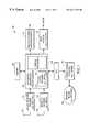
- FIG. 1is a diagram illustrating a video and graphics system 100 in which one embodiment of the invention can be practiced.
- the system 100includes an integrated graphics and video processor 110 , an analog receiver decoder 122 , a digital television (TV) receiver 124 , a high (or standard) definition display monitor, a video encoder 134 , a memory 140 , and a central processing unit (CPU) 150 .
- Additional elementsinclude a communication interface 160 , and a network medium 165 .
- the integrated graphics and video processor 110is a high performance processor dedicated for graphics and video processing. It can be used in a number of applications including set-top boxes and other television (TV)-based digital systems.
- the integrated graphics and video processor 110includes a digital decoder 170 and a display processor 180 .
- the digital decoder 170receives digital multimedia data from standards such as Moving Picture Expert Group (MPEG) standard MPEG-2.
- MPEGMoving Picture Expert Group
- the digital decoder 170passes the decoded data to the display processor 180 and/or other units for further processing or storage.
- the display processor 180processes the video and/or graphic data and generate the result to the high (or standard) definition display monitor 132 and video encoder 134 .
- the analog receiver decoder 122receives analog signal via the antenna 123 and processes analog video signals and presents digital data to the integrated graphics and video processor 110 in proper formats.
- the analog decoder 122captures and digitizes the analog video signals into digital data.
- the analog video signalis an NTSC or PAL signal
- the decoded digital data formatis YCbCr 4:2:2 digital video.
- other types of analog video signals and digital data formatscan be used.
- the digital TV receiver 124receives digital data via the antenna 125 and processes the digital data and decodes the data into appropriate channels and formats to the integrated graphics and video processor 110 .
- the digital datafollow the Moving Picture Expert Group (MPEG) standards.
- MPEGMoving Picture Expert Group
- Examples of the MPEG standardsinclude MPEG-2, MPEG-4, and MPEG-7.
- the digital datamay include multimedia information such as moving picture and stereo audio.
- the high (or standard) definition display monitor 132is a display monitor that can display images/video/graphics information at high resolution or low resolution at various scanning modes such as interlaced or progressive (non-interlaced) scanning mode.
- the video encoder 134is a device or an equipment that converts the digital output from the integrated graphics and video processor 110 into appropriate video signals.
- the video encoder 132provides input to a TV set and/or a video cassette recorder (VCR). As is known by one skilled in the art, other video equipment can be used.
- VCRvideo cassette recorder
- the memory 140stores code, data, and other information for use by the integrated graphics and video processor 110 and other devices.
- the memory 140includes a number of synchronous dynamic random access memory (SDRAM) devices.
- SDRAMsynchronous dynamic random access memory
- the CPU 150is a processor that performs general processing functions.
- the integrated graphics and video processor 110is designed to interface with a number of microprocessors.
- these microprocessorsinclude the Motorola MC6833x, the Motorola MC68340/L64x08, the ST20TPI/ST20-T, the Motorola MCF5206, the Hitachi SH-2/3, and the DEC StrongARM SA-110.
- DSPdigital signal processors
- RISCsreduced instruction set computers
- the communication interface 160provides interface to communication devices or media to the CPU 150 .
- the communication interface 160may include telephone modem interface, network interface, radio transceivers, fiber optics transceivers, etc.
- the network medium 165provides a communication medium for information transmission and reception. In one embodiment, the network medium 165 is the Internet.
- FIG. 2is a diagram illustrating a display processor 180 shown in FIG. 1 according to one embodiment of the invention.
- the display processor 180includes a filtering and format conversion unit (FFCU) 210 , a graphics processor 215 , a memory interface 220 , a video interface 230 , a memory buffer 240 , a host interface 250 , and a synchronization (SYNC) circuit 260 .
- FFCUfiltering and format conversion unit
- SYNCsynchronization
- the FFCU 210receives the graphic/video data from the memory 140 via the memory interface 220 and the memory buffer 240 and generates the result to the video encoders via the video interface 230 .
- FFCU 210performs a comprehensive set of functions on two-dimensional pixel data in a variety of pixel map formats. These functions include horizontal and vertical scaling and filtering.
- the FFCUalso is used to convert various source display formats to destination display formats.
- the graphics processor 215performs additional graphics and image operations such as aspect ratio correction, and anti-flickering.
- the memory interface 220interfaces to the memory 140 (FIG. 1) to provide data to the FFCU 210 , the graphics processor 215 and the video interface 230 .
- the memory interface 220includes circuits to allow access to the memory 140 at high bandwidth to accommodate the processing speed of the graphics processor 210 .
- the video interface 230performs the final blending and composing operations of the input sources of the display processor 180 .
- the video interface 230also generates proper video timing signals to video encoders such as CCIR-601 synchronization, vertical and horizontal synchronization signals.
- the video interface 230generates display data to the video encoders and receives background (BGND) video from other video sources.
- BGNDbackground
- the memory buffer 240stores temporary data in properly sized buffers for use by the CPU 150 and the graphics processor 210 .
- the memory buffer 240manages the buffer needs of the background graphics, scaled video, scaled graphics, cursor and configuration registers. In one embodiment, these buffers are implemented by fast static random access memory (SRAM).
- SRAMfast static random access memory
- the host interface 250provides interface to the CPU 150 .
- the host interface 250generates interrupt signals to the CPU 150 for end of scan line, beginning of field, or end of field.
- the host interface 250also allows the CPU 150 to configure and initialize the display processor 180 via a set of configuration and control registers.
- the SYNC unit 260provides horizontal (H), vertical (V), and field (F) information to be used in video synchronization.
- H, V, and F informationcan be generated in a programmable manner so that a number of video formats can be accommodate. Examples of these video formats include CCIR-601, NTSC, PAL.
- FIG. 3is a diagram illustrating a filtering and format conversion unit (FFCU) 210 according to one embodiment of the invention.
- the FFCU 210includes a horizontal processor (HP) 310 , a vertical processor (VP) 320 , and a up-conversion unit 330 .
- HPhorizontal processor
- VPvertical processor
- up-conversion unit 330up-conversion unit
- the HP 310 , the VP 320 , and the up-conversion unit 330all interface to the memory interface 220 (FIG. 2 ).
- the up-conversion unitgenerates output to the video interface 230 (FIG. 2 ).
- the HP 310receives image data from MPEG decoder 170 either directly or from the memory 140 via the memory interface 220 .
- the HP 310receives the image data directly from the MPEG decoder 170 (shown in FIG. 1 ).
- the HP 310processes the image data horizontally.
- the processed image dataare the written back to the memory 140 to be processed by the subsequent stage.
- the VP 320obtains image data from the memory 140 and processes the image data vertically. To achieve efficiency, the VP 320 processes image data in vertical patches. The vertical patches are fetched from the memory 140 and stored in a buffer inside the VP 320 . Since the vertical processing is performed on the on-chip buffers, the processing rate is fast to achieve high quality filtering results. The VP 320 writes the result back to the memory 140 for subsequent processing.
- the up-scaling unit 330performs up-scale operations when required.
- the up-scaling unit 330can also bypass the up-scale processing.
- the resultis then passed to the video interface 230 for display.
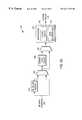
- FIG. 4is a diagram illustrating a vertical processor (VP) 320 shown in FIG. 3 according to one embodiment of the invention.
- the VP 320includes a VP read interface circuit 410 , a VP feed circuit 420 , a de-interlace circuit 430 , a down-scale VP filter 440 , a VP receive circuit 450 , and a VP write interface circuit 460 .
- the VP read interface circuit 410interfaces to the memory interface 220 to read image data from the memory 140 .
- the VP read interface circuit 410reorganizes the image data to be ready for vertical processing.
- the VP feed circuit 420mainly converts the parallel loaded data into a sequential series of pixels to facilitate processing.
- the de-interlace circuit 430performs de-interlace operations when converting the image format from interlace to progressive formats.
- the down-scale VP filter 440performs the down-scale operation on the image data.
- the de-interlace circuit 430 and the down-scale VP filter 440operate in two separate data paths in a mutual exclusive manner. As is known by one skilled in the art, the configuration may be modified to allow both circuits to operate in parallel to achieve both results at the same time if necessary.
- the VP receive circuit 450selects and organizes results from the de-interlace circuit 430 and the down-scale VP filter 440 .
- the VP write interface circuit 460stores the selected results in a buffer, re-organizes the processed image data and writes the final result back to the memory interface 220 .
- FIG. 5Ais a diagram illustrating a VP read interface circuit 410 shown in FIG. 4 according to one embodiment of the invention.
- the VP read interface circuit 410includes a re-order buffer 510 , a multiplexer 520 , a corner turn circuit 530 , a multiplexer 540 , and a read buffer 550 .
- the VP read interface circuit 410provides support for processing either interlaced images or progressive images.
- the VP read interface circuit 410reads the image data from the memory 140 via the memory interface 220 .
- the read image datacan be re-ordered by the re-order buffer 510 or bypassed around the re-order buffer 510 .
- the re-order buffer 510merges the field separated data of progressive frames from the memory 140 into correct line order.
- the multiplexer 520allows selection of the re-ordered image data or the original image data from the memory 140 .
- the corner turn circuit 530transposes the rows of pixels into columns of pixels for vertical processing.
- the multiplexer 540allows selecting between the transposed data or the selected data from the multiplexer 520 .
- the read buffer 550stores the image data in column format (for down-scale filtering) in a column buffer 552 or row format (for de-interlacing) in a row buffer 554 .
- FIG. 5Bis a diagram illustrating a re-order buffer 510 shown in FIG. 5A according to one embodiment of the invention.
- the re-order buffer 510includes line buffers 512 , 514 , 516 , and 518 .
- the memory 140stores image data in two fields: an even field corresponding to even lines, and an odd field corresponding to odd lines.
- the two fieldsare stored in two areas in the memory 140 .
- all lines of data in a fieldcome from the same area of the memory 140 .
- each subsequent linecomes alternatively from each of the two areas of the memory 140 .
- the image dataare transferred two eight byte words in contiguous cycles per transaction.
- a pair of transactionsis initiated, one to each of the two memory controller buffers.
- Each transactioncontains a pair of lines, both being either even line numbers or odd numbers.
- the line buffers 512 and 514stores two even lines (A,C) and two odd lines (B,D), respectively.
- the line buffer 516is essentially a register to load the alternating lines C and D.
- the line buffer 518stores the re-ordered data A, B, C, and D. In this manner, the re-order buffer 510 accepts eight interlaced lines from the memory 140 and re-orders the lines in a non-interlaced manner to send to the corner turn in each pass.
- FIG. 5Cis a diagram illustrating a corner turn circuit 530 show in FIG. 5A according to one embodiment of the invention.
- the corner turn 530includes an eight-by-eight array of register units to perform a two-dimensional data steering logic function, and a multiplexer 538 .
- the 8 ⁇ 8 register unitsform a two-dimensional array of 8 ⁇ 8, where each element corresponds to an 8-bit pixel. Eight words (eight pixels per word) are shifted into the array one word at a time. Once the array has been loaded, the resultant data are shifted out to the right one word at a time to generate the column elements.
- the arrayalso supports row transferred data.
- the multiplexer 538selects between the row and column data.
- the 8 ⁇ 8 arrayincludes 64 identical elements, represented by an element 532 .
- the element 532includes a multiplexer 533 and a register 535 .
- the multiplexer 533allows selecting data from the left or from above as shown in the 2-D array.
- the output of the registeris directed to the element to the right and below.
- the register 535is enabled for shifting by an array shift enable (ARRAY_SH_EN) control signal.
- the control signal for the multiplexer 533 and 538is a flow direction (FLOW_DIR) control signal that controls the selection of row or column data.
- FIG. 6is a diagram illustrating a VP feed circuit 420 shown in FIG. 4 according to one embodiment of the invention.
- the VP feed circuit 420includes parallel load shift registers 610 and 620 , and a shift register 630 .
- the VP feed circuit 420essentially performs parallel to serial conversion.
- the de-interlace circuit 430 and the down-scale filter 440expect consecutive pixels (either horizontally or vertically) to be serially fed to their respective inputs.
- the on-chip buffer 550 (FIG. 5A) in the VP read interface circuit 410stores multiple adjacent pixels in parallel.
- the VP feed circuit 420provides a shifting mechanism to convert the parallel data from the on-chip buffer 550 to serial form for feeding the de-interlace circuit 430 and the down-scale filter 440 .
- the parallel load shift registers 610 and 620provide the serial data for the down-scale filter 440 .
- the parallel load shift registers 610 , 620 and the shift register 630provide the serial data for the de-interlace circuit 430 .
- Each of the parallel load shift registers 610 and 620loads the pixel data from the VP read interface circuit 410 in parallel and then shifts the loaded data serially.
- the shift register 630acts as an additional shifter.
- the pixel replication necessary for the down scale filtercan be accomplished by asserting the valid data signal for the shift register output and de-asserting the shift control signal.
- the de-interlace circuit 430requires three lines to be fed, one pixel from each line in each cycle.
- the de-interlace circuit 430traverses a patch horizontally from left to right. After each line has been processed, the de-interlace circuit 430 moves down by two lines. Therefore, the data in the bottom line will repeat as the top line in the next traversal. This is accomplished by shifting the data from the top line into the shift register for the bottom line at the same time as the data is being shifted into the de-interlace circuit 430 .
- new pixelsare loaded into the parallel load shift registers 610 and 620 from words read from the VP read interface circuit 410 .
- the VP feed circuit 420In the de-interlace mode, some situations require the VP feed circuit 420 to replicate the data in one line for another line. This is accomplished by first loading the parallel load shift registers 610 and 620 , each with a line. A dummy shifting cycle is gone through with no valid data fed into the de-interlace circuit 430 to shift the serial data from the parallel load shift register 610 into the shift register 630 . At the same time, the data is re-circulated back into the parallel load shift register 610 to preserve the original data for the line. After this step, the parallel load shift register 610 and the shift register 630 contain the same data and the parallel load shift register 620 contain data from another line.
- FIG. 7is a diagram illustrating a de-interlace circuit shown in FIG. 4 according to one embodiment of the invention.
- de-interlacingThe basic concept of de-interlacing is to convert an interlaced image into a non-interlaced (or progressive) image with the same number of lines in the frame at 60 Hz refresh rate as the number of lines in both fields of the interlaced image at the field refresh rate of 30 Hz.
- the de-interlacinginvolves considerations of both spatial and temporal information.
- FIG. 7shows a 3 ⁇ 3 window of pixel data used in the de-interlacing.
- the pixel datacorresponds to two fields n and n ⁇ 1.
- the center pixelcorresponds to field n ⁇ 1 while the surrounding pixels correspond to field n.
- the pixel elements used in the de-interlacing circuitincludes p n (i ⁇ 1,j ⁇ 1), p n (i ⁇ 1,j), p n (i ⁇ 1,j+1), p n ⁇ 1 (i,j), p n (i+1, j ⁇ 1), p n (i+1,j), and p n (i+1,j+1).
- the de-interlacing operationfirst determines if there is sufficient motion in the pixel data. If there is no significant motion, the de-interlaced pixel is p n ⁇ 1 (i,j). If there is sufficient motion, the de-interlaced pixel is the interpolated pixel.
- the pseudocode for computing ELAis:
- the de-interlace circuit 430includes a de-interlace core circuit 710 , registers 722 , 724 , 726 , 732 , 734 , and 736 , and multiplexer 738 .
- the registers 722 , 724 and 726receive the pixel data from line i ⁇ 1 in field n to provide the pixels p n (i ⁇ 1,j ⁇ 1), p n (i ⁇ 1,J), and p n (i ⁇ 1,j+1), respectively.
- the registers 732 , 734 , and 736receive the pixel data from line i+1 in field n to provide the pixels p n (i+1,j ⁇ 1), p n (i+1,j), and p n (i+1,j+1).
- the de-interlace core circuit 710receives the pixel p n ⁇ 1 (i,j) from line i and field n ⁇ 1 and the other six pixel data to generate the motion and interpolation results.
- the de-interlace core circuit 710includes a motion detector 712 and an ELA interpolator 714 .
- the multiplexer 738selects between the pixel p n ⁇ 1 (i,j) and the interpolated result based on the motion detector result.
- FIG. 8is a diagram illustrating a de-interlace core circuit 710 shown in FIG. 7 according to one embodiment of the invention.
- the de-interlace core circuit 710includes a motion detector 712 and an interpolator 714 .
- the motion detector 712includes an adder array 810 , a pipeline register array 812 , a subtractor array 814 , an absolute array 816 , a comparator array 818 , a register array 820 , and a motion logic circuit 822 .
- the adder array 810performs the addition inside the abs( ) shown in equations (3a), (3b) and 3(c).
- the resulting sumsare stored in the pipeline register array 812 to synchronize with the interpolator 714 .
- the subtractor array 814subtracts the pixel data pn(I,j) from each of the sums.
- the absolute array 816takes the absolute of the differences to generate the quantities A, B, and C in equations (3a), 3(b) and 3(c).
- the comparator array 818compares each of the quantities A, B, and C with the threshold value as shown in the test condition (3d). The results of the comparison are stored in the register array 820 .
- the motion logic circuit 822combines
- the interpolator 714includes a subtractor array 830 , an absolute array 832 , a comparator array 834 , a pipeline register array 836 , and a data selector 838 .
- the subtractor array 839 and the absolute array 832perform the operations in equations (4a), (4b), and (4c).
- the comparator array 834performs the various comparisons as shown in equations (4d), (4e), and (4f).
- the pipeline register array 836stores the result of the comparison.
- the data selector 838generates the AELA interpolated value using the comparison results and the sum results from the pipeline register array 812 in the motion detector 712 .
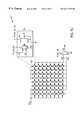
- FIG. 9Ais a diagram illustrating vertical patch organization according to one embodiment of the invention.
- the organizationincludes an image region 910 .
- the image regionincludes an exemplary vertical patch 912 .
- the image region 910shows a portion of the image that contains a number of vertical patches.
- Patchesare rectangular sections, sometimes referred to as tiles, of an image. Patches overlap to provide support for the filters when computing data along the edge of the patch to eliminate edge effects.
- the region 910consists of a number of vertical patches that are adjacent on columnwise but are overlapped on rowwise. Each vertical patch is organized as 16 ⁇ 64, i.e., each vertical patch is 16-pixels wide and 64-pixels high. As is known by one skilled in the art, other patch sizes are possible. The choice the patch size depends on factors such as processing overhead, memory access times, filter size, etc. and is selected to optimize the overall performance.
- the height of a vertical patchmay be less than 64 when it is at the bottom edge of the image or after the patch has been scaled down vertically.
- a vertical patchconsists of an active source region being processed vertically plus additional lines for the filter support.
- the actual number of lines processedis equal to patch height-total support. Therefore there is an overhead of (total support) lines so that the edges of the active part of the patch can be correctly computed independent of any other patch.
- the vertical patch 912includes 16 vertical strips, each strip is one-pixel wide and 64-pixels high.
- the vertical patch 913has two overlapped sections for filter support, one is at the top and one is at the bottom. For a filter size of 20, the top support is 9-pixel high and the bottom support is 10-pixel high for a total support height of 19. Therefore, the height of the active source region is 45.
- Each vertical stripis processed by a vertical filter having a filter size of 20.
- the vertical filterprocesses the image data segments by segments from top to bottom of each patch. For example, a segment 914 having 20 pixels corresponds to the top of the vertical patch 912 and a segment 916 having 20 pixels corresponding to the bottom of the vertical patch 912 .
- the vertical filtertraverses from the segment 914 down to the segment 916 .
- the patch filtering described aboveis also applicable to other filtering directions as well. This includes the horizontal filter. Essentially, the use of patches improves performance by providing fast access to high-speed buffers, especially when the buffers are implemented on-chip. Patches are also reasonably sized so that they are not too costly to implemented.
- Patches of image datacan be processed, or filtered, by either the vertical filter or horizontal filter. Patches are transferred from memories or any other processing unit to a fast local buffer.
- the local bufferis preferably implemented as an on-chip buffer; however, off-chip buffers with fast access times are possible. From the local buffer, patches can be processed by the corresponding processor such as the horizontal or vertical processor. After the processing, the processed patches can be written back to the memory or to another processing unit.
- the typical processing stepsinclude: (1) filtering using a finite impulse response (FIR) filter to bandlimit the input image data, (2) interpolating to re-sample the filtered data.
- FIRfinite impulse response
- a complete down-scale filteringusually involves both horizontal filtering and vertical filtering, corresponding to scaling in the horizontal and vertical directions.
- the processingis carried out in two passes: horizontal and vertical.
- horizontal and verticalDuring the horizontal pass, only horizontal processing is performed in patches.
- vertical passonly vertical processing is performed in patches. In between passes, intermediate results are written into the memory.
- the horizontal and vertical processingare performed at the same time within a patch.
- FIG. 9Bis a diagram illustrating a down scale vertical filter 440 shown in FIG. 4 according to one embodiment of the invention.
- the down scale vertical filter 440includes a low pass filter 920 and an interpolator 970 .
- the low pass filter 920is a non-recursive filter that performs a weighted sum operation on the pixel data. In one embodiment, the filter size is 20.
- the interpolator 970is also a non-recursive filter. The interpolator 970 uses a digital differential analyzer (DDA) to decide how to precisely position the filter on the input data for each output result.
- the interpolator 970essentially performs decimation and interpolation.
- the interpolator 970is similar to the horizontal interpolator. The details of the interpolator 970 is described in FIGS. 12A and 12B.
- the combination of the low pass filter 920 and the interpolator 970accomplishes the down scale operation.
- the low pass filter 920prevents aliasing on the decimation/interpolation.
- the low pass filteris an N-tap FIR filter
- FIG. 9Cis a diagram illustrating a low pass filter 920 shown in FIG. 9B according to one embodiment of the invention.
- the low pass filter 920includes seventeen registers 930 0 through 930 16 , eight two-input adders/subtractors 940 0 through 940 7 , nine multipliers 950 0 though 950 8 , and nine-input adder 960 .
- the low pass filterperforms the weighted sum operation of the 17-tap non recursive filter, or finite impulse response (FIR) filter. Because the filter is linear phase, the taps are symmetrical. Consequently, the number of multipliers can be halved.
- FIRfinite impulse response
- the registers 930 0 through 930 16store the input pixel data a 0 through a 16 , respectively.
- the adders 940 0 through 940 7perform the subtractions as shown in the parentheses in equation (6) above.
- the multipliers 950 0 through 950 8perform the multiplications of the coefficients c 0 through c 8 with the corresponding results as shown in equation (6) to generate nine products.
- the adder 960adds the nine products to produce the filter output LPOUT.
- the low pass filter 920also performs rounding and saturation to 0-255. It also has a bypass option, which takes the value a 9 and sends it out.
- FIG. 9Dis a diagram illustrating an interpolator 970 shown in FIG. 9B according to one embodiment of the invention.
- the interpolator 970includes a VP digital differential analyzer (DDA) 992 , a VP interpolator coefficient storage (VP_ICOEFF) 994 , and four registers 980 0 through 980 3 , four adders 985 0 through 985 3 , and a 4-input adder 990 .
- the VP_DDA 992 and the VP_ICOEFF 994are similar to the horizontal filter and are described later.
- the interpolatorcontains 4 taps, each tap requires a coefficient for computation. A set of 4 coefficients can be selected for the interpolating.
- the filtersupports 16 phases, so there are 16 sets of 4 coefficients. When operating the VP_DDA 992 provides the phase setting with which one of the sets of 4 coefficients is selected from such 16 sets.
- the VP_ICOEFF storage 994stores these sets of coefficients.
- the interpolator 970is a 4-tap polyphase non recursive filter.
- the filter coefficientsare fixed and determined by using a cubic spline algorithm.
- the first and the last coefficientsare 8-bit signed, and the middle two are 11-bit unsigned.
- the interpolator 970also performs rounding and saturation and has a bypass feature.
- the interpolatorperforms the following operation:
- VF_OUTb 0 * d 0 + b 1 * d 1 + b 2 * d 2 + b 3 * d 3
- FIG. 10is a diagram illustrating a VP receive circuit 450 and a VP write interface circuit 460 shown in FIG. 4 according to one embodiment of the invention.
- the VP receive circuit 450includes multiplexers 1010 , 1020 , and 1030 , two serial-to-parallel converters 1012 and 1022 , and two registers 1014 and 1024 .
- the VP write interface circuit 460includes a write buffer 1040 , a corner turn circuit 1050 , a multiplexer 1055 , and a register 1060 .
- the VP receive circuit 450receives the serial pixel data from the de-interlace circuit and the down-scale filter and converts into parallel words.
- the VP receive circuit 450also handles the case of down-scaling to a progressive result. For efficiency, transactions to the memory controller use pairs of words. These words correspond to both lines being even or both lines being odd. Because the data coming out of the down-scale filter and the de-interlace circuit represents consecutive lines in the frame, the VP receive circuit 450 steers each sequentially received pixel to the appropriate place in the write buffer 1040 in the VP write interface circuit 460 .
- the two multiplexers 1010 and 1020select the pixel data from the down-scale filter and the de-interlace circuit.
- the multiplexer 1010selects pixel data from the down-scale filter at the right position and the bottom field in the interlace circuit.
- the multiplexer 1020selects pixel data from the down-scale filter at the left position and the top field in the interlace circuit.
- the serial-to-parallel converters 1012 and 1022converts the serial data selected by the multiplexers 1010 and 1020 , respectively, into parallel word.
- the parallel datais then loaded into the registers 1014 and 1024 .
- the multiplexer 1030selects from the right and left filter positions for the down-scale filtering or the bottom and top field for the de-interlace operation.
- the write buffer 1040stores the parallel words in a 128 ⁇ 8 byte buffer.
- the corner turn circuit 1050performs a transposition, i.e., it converts the row pixel data into column pixel data. Since the pixel data from the down-scale filter is the column data due to the transposition in the read interface circuit, the corner turn circuit 1050 essentially restores the pixel organization to the row-ordered data to be written into the memory.
- the multiplexer 1055selects between the transposed data or data from the write buffer 1040 .
- the register 1060stores the result to be written into the memory 140 .
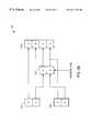
- FIG. 11is a diagram illustrating a horizontal processor (HP) 310 shown in FIG. 3 according to one embodiment of the invention.
- the HP 310includes an HP control circuit 1110 , an HP core circuit 1120 , an HP snoop circuit 1160 , an HP write circuit 1170 , and a memory bus 1080 .
- the HP control circuit 1110generates timing and control signals to the HP core circuit 1120 and the HP write circuit 1170 .
- the HP control circuit 1110also receives status information from the HP snoop circuit 1160 .
- the HP core circuit 1120performs the core operation for the horizontal filter.
- the HP snoop circuit 1160snoops the data written from the MCE to the MIF.
- the format of the MCE's datais in macroblock units, which in turn are split into two separate sets of writes, a top and a bottom write. Each set of writes contains 16 words (64 bits) of Y, 4 words of Cb, and 4 more words of Cr.
- the HP snoop circuit 1160snoops on the descriptor post, data write and buffer retire. In the descriptor post, the HP snoop circuit 1160 extracts information on where the data is stored in the frame buffer area.
- the HP write circuit 1170writes the processed pixel data from the HP core circuit 1120 to the MIF via the memory bus 1080 .
- the writingcan be done for an entire macroblock.
- the HP core circuit 1120performs the core horizontal filtering operation.
- the HP core circuit 1120includes an HP input buffer (HP_INBUF) 1132 , an HP feed circuit (HP_FEED) 1134 , two HP low pass filters (HP_LOWPASS) 1136 and 1138 , two HP interpolators (HP_INTERP) 1142 and 1144 , an HP receive circuit (HP_RECEIVE) 1146 , an HP output buffer (HP_OUTBUF) 1152 , and HP digital differential analyzer (DDA) 1148 , and an HP coefficient buffer (HP_ICOEFF) 1150 .
- HP_INBUFHP input buffer
- HP_FEEDHP feed circuit
- HP_LOWPASStwo HP low pass filters
- HP_INTERPHP interpolators
- HP_RECEIVEHP receive circuit
- HP_OUTBUFHP output buffer
- DDAHP digital differential analyzer
- HP_ICOEFFHP coefficient buffer
- the HP_INBUF 1132stores the macroblock data in a 512 ⁇ 64 RAM organized as an array of 32 ⁇ 128 bytes.
- the HP_FEED 1134has two 64-bit registers, each of which loads in 64 bits at once from the HP_INBUF 1132 and shifts out 8 bits at a time to the HP_LOWPASS 1136 and 1138 .
- the HP_FEED 1134includes two 8-bit shift registers to send out two parallel byte streams in the same horizontal position.
- Each of the HP_LOWPASS filters 1136 and 1138is essentially similar to the lowpass filter in the down-scale vertical filter 440 .
- each of the HP_LOWPASS filters 1136 and 1138is a 17-tap non recursive filter.
- Each of the HP_INTERP circuits 1142 and 1144is also similar to the interpolator in the down-scale vertical filter 440 .
- the HP_RECEIVE circuit 1146contains two 64-bit registers. Each of these register banks updates 8 bits at a time with the incoming filter results. Every 8 cycles, the accumulated 64-bit result is written into the HP_OUTBUF circuit 1152 . The HP_OUTBUF 1152 buffers the result pixel data. The HP_RECEIVE circuit 1146 also reads back the data from the HP_OUTBUF when there is an odd number of data produced.
- the HP_DDA 1148performs the down sampling phase and skip calculations.
- the HP_DDA 1148updates the HP_ICOEFF 1150 which in turns provides information to the HP_INTERP 1144 .
- FIG. 12Ais a diagram illustrating an example for a digital differential analyzer (DDA) according to one embodiment of the invention.
- DDAdigital differential analyzer
- the HP_DDA 1148has 4 bits of decimal precision to calculate the correct phase (0 through 5), and it accumulates the error separately.
- the SSis the downscaling factor, truncated to the nearest ⁇ fraction (1/16) ⁇ .
- the UNis the number of macroblocks that the DDA will undershoot the target by, using SS as the step value.
- the ONis the number of macroblocks that the DDA will overshoot the target by, using SS+1 as the step value.
- the expressions for SS, UN, and ONare:
- the down scalingis from 10 to 6.
- the SSis 1 ⁇ fraction (10/16) ⁇ .
- the UNis 4 and the ON is 2.
- the DDAstarts at the pixel DO where the error is 0.
- the DDAsteps through at 1 ⁇ fraction (10/16) ⁇ step size (truncated to the nearest 1 ⁇ fraction (10/16) ⁇ ).
- the DDAreaches 9 ⁇ fraction (5/16) ⁇ with undershoot error of 2.
- the filtersrun at one input pixel per cycle, so a pixel counter starts at 0 and counts 1, 2, 3, etc. Every time this value matches the integer part of the DDA, the corresponding phase is used to get the appropriate interpolation taps, and the result is taken.
- the DDA value and the errorare accumulated across an entire line of data.
- the DDAshould be required to restore its state. For example, after the last pass of luma filtering, the DDA saves its values into a register, and it loads up the old chroma DDA settings before it filters the chroma.
- FIG. 12Bis a diagram illustrating a DDA shown in FIG. 11 according to one embodiment of the invention.
- the DDA 1148includes a DDA core circuit 1210 and two setting saving circuits 1211 and 1212 .
- the DDA core circuit 1210generates the integer and the phase values.
- the DDA core circuit 1210includes adders 1220 and 1234 , two 4-input multiplexers 1222 and 1236 , 2-input multiplexers 1224 , 1230 and 1238 , a DDA register 1226 , a subtractor 1228 , a multiplexer 1230 , and an error register 1240 .
- the adder 1220adds the SS value by incrementing the integer and phase output values with the error.
- the adder 1234adds the UN or ON value to the error value.
- the 4-input multiplexers 1222 and 1236allow the update using the dda_update[1:0] select signal as follows: 0 (re-circulate value), 1 (increment by one step value), 2 (load saved luma settings), and 3 (load saved chroma setting).
- the multiplexers 1224 and 1238allow resetting the DDA and error to zero and is controlled by the dda_zero signal.
- the DDA register and the error register 1226 and 1240stores the DDA results (integer and phase) and the error value.
- the subtractor 1228subtracts the number of valid pixels processed, sub val[6:0] from the integer portion of the DDA result so that the next run can start with a pixel count of 0.
- the setting saving circuits 1211 and 1212save the DDA result (adjusted by the sub_val[6:0]) and the error, respectively.
- FIG. 12Cis a diagram illustrating a setting saving circuit 1211 / 1212 shown in FIG. 12B according to one embodiment of the invention.
- the setting saving circuit 1211 / 1212includes multiplexers 1252 , 1254 , and 1259 , and two registers 1256 and 1258 .
- the multiplexers 1252 and 1254select the start value for chroma and luma processing, respectively.
- the start valueis the adjusted DDA result (for 1211 ) or the error value (for 1212 ).
- the registers 1256 and 1258store the settings for chroma and luma, respectively. The outputs of the registers are fed back to the multiplexers 1252 and 1254 , respectively, for re-circulating of the settings.
- the multiplexer 1259selects between chroma and luma saved settings.
- FIG. 13Ais a diagram illustrating an organization of the HP input buffer shown in FIG. 11 according to one embodiment of the invention.
- the HP input bufferis organized as 32 ⁇ 128 bytes and stores the macroblocks for Y, Cb, and Cr.
- the HP input bufferstores eight 16 ⁇ 16 Y macroblocks, sixteen 8 ⁇ 8 Cb macroblocks, and sixteen 8 ⁇ 8 Cr macroblocks.
- the macroblocksare stored to allow processing of two consecutive patches as shown in the shaded boxes of FIG. 13 A.
- the processing of the patchesallows the replication of overlapped segments as the filter traverses.
- the patch configurationmay replicate the support of 9 or 19 width (or height for vertical filter).
- FIG. 13Bis a diagram illustrating a patch configuration according to one embodiment of the invention.
- the patch configurationincludes patch 1310 , patch 1320 , and patch 1330 .
- the patch 1310corresponds to the first patch (or the rightmost patch) in the processing.
- the duplicated 9 componentsare stored in the dashed lines on the left of the patch.
- the patch 1320corresponds to the middle patch in the processing.
- the previous 19 components (old data)are stored in the dashed lines for the previous 19 components.
- the patch 1330corresponds to the last patch (or the leftmost patch) in the processing.
- the previous 19 components (old data)are stored on the left of the patch and the duplicated 10 components are stored on the right of the Y macroblock.
- first_patchThis indicates duplication on the left of 9 components. Otherwise, the patch is either the middle patch or the last patch and the previous 19 components are read out.
- tail_ptr[3:0]This indicates the last column of the input buffer.
- chromathe full value (0-15) is used, for luma, the MSB is cut off, so the value is between 0-7.
- FIG. 13Cis a diagram illustrating an example for a patch processing according to one embodiment of the invention. This example shows the information given for each patch execution in a picture with a region of interest (ROI) of 10 macroblocks. There are three patches: the first patch, the second patch, and the last patch.
- ROIregion of interest
- the first patchhas Y macroblocks from 0 to 3, and chroma macroblocks from 0 to 3.
- the head_ptr_y and head_ptr_care both 0, and the tail_ptr is 3.
- the second patchhas Y macroblocks from 4 to 7, and chroma macroblocks from 4 to 7.
- the second patchstores the previous 19 components for both Y and chroma macroblocks, occupying the Y macroblock 2 and the chroma macroblock 1 . Therefore, the head_ptr_y is 2 and the head_ptr_c is 1.
- the tail_ptris 7 pointing to the last column in the patch for both Y and chroma macroblocks.
- the third patchhas Y macroblocks 0 to 1 in the next storing cycle of the input buffer, and chroma macroblocks 8 and 9. Since the third patch is the last patch, it also stores the previous 19 components, occupying Y macroblock 6 and chroma macroblock 5. Therefore, head_ptr_y is 6, head_ptr_c is 5, and tail_ptr is 9 (for chroma) and 1 (for luma).
- FIG. 14is a diagram illustrating an up-scaling unit 330 according to one embodiment of the invention.
- the up-scaling unit 330includes a filter coefficient multiplexer 1410 , a control logic circuit 1420 , a Y vertical filter 1430 , a Y horizontal filter 1440 , a chroma vertical filter 1450 , and a chroma horizontal filter 1460 .
- the filter coefficient multiplexer 1410provides the filter coefficients for the luma and chroma processing chains.
- the control logic circuit 1420provides timing and control signals to the various filters used in the processing chain.
- the Y vertical filter 1430 and the Y horizontal filter 1440performs up-scaling operations on luma vertical data and then luma horizontal data, respectively.
- the chroma vertical filter 1450 and the chroma horizontal filter 1460performs up-scaling operations of chroma vertical data and chroma horizontal data.
- the results of the Y and chroma processing chainsare sent to the video interface 230 .
- the vertical and horizontal filters 1430 , 1450 and 1440 , 1460may be implemented using the same architecture as described in FIGS. 9B, 9 C, and 9 D.
- the vertical filters 1430 and 1450can be implemented as an in-line N-tap multirate interpolator where N is a function of the number of pixels in the source image scan line.
- the tap pixel dataare provided from a line buffer with size sufficiently large to hold a number of filter lengths. In one embodiment, the vertical in-line tap size is 2 or 3 and the line buffer size is 1440-pixels long.
- the data to the Y and chroma vertical filterscan be from either external memory buffer (e.g., memory 140 ), or on-chip buffers.
- the output of the vertical filteris fed directly to the corresponding horizontal filter.
- the scaling unitscan be used to scaled the image data components (e.g., luma, chroma) separately for color format conversion, such as conversion between the 4:2:2 and 4:2:0 formats.
- image data componentse.g., luma, chroma
- the scaling units and the de-interlace circuitcan be used in display format conversion from a source format to a destination format.
- the source formatmay include 240 P, 480 I, 480 P, 720 P, and 1080 I
- the destination formatmay include 480 I, 480 P, 720 P, and 1080 I, each with 60 frames per second (fps), where P denotes progressive and I denotes interlaced.
- the source 720 P imageis down-scaled to a 540 P image using the down-scale filter.
- each progressive frameis converted into a field for interlaced display.
- the filterfetches several lines from the progressive frame, some lines residing in the on-chip buffer while other lines residing in the external memory. Since each field has one of two possible positions: top or bottom, a frame has to be adjusted before forming the field data. This is handled by the filter and format conversion circuit which adjusts the starting position of the filter one line down from the starting position of a top field.
- FIG. 15Ais a table illustrating format conversion from all input formats to high resolution displays according to one embodiment of the invention.
- the source formatincludes a source low resolution progressive (SLRP), low resolution interlaced (SLRI), high resolution progressive (SHRP), and high resolution interlaced (SHRI).
- the destination formatincludes destination high resolution progressive (DHRP) and destination high resolution interlaced (DHRI).
- the tableshows processing steps to perform the format conversion. These processing steps invoke the scaling and/or the de-interlacing operations as appropriate.
- the processingcan be done by hardware or software or any combination of hardware and software.
- the up-scaling unitreads a frame in the memory.
- the up-scaling unitup-scales the image to a frame image.
- the display controllerdisplays the resulting frame image.
- the up-scaling unitreads a frame in memory.
- the up-scaling unitup-scales the frame image to a field image.
- the display controllerdisplays the resulting field image. etc.
- FIG. 15Bis a table illustrating format conversion from all input formats to low resolution displays according to one embodiment of the invention.
- the source formatincludes a source low resolution progressive (SLRP), low resolution interlaced (SLRI), high resolution progressive (SHRP), and high resolution interlaced (SHRI).
- the destination formatincludes destination low resolution progressive (DLRP) and destination high resolution interlaced (DLRI).
- the tableshows processing steps to perform the format conversion. These processing steps invoke the scaling and/or the de-interlacing operations as appropriate.
- the processingcan be done by hardware or software or any combination of hardware and software.
- the up-scaling unitreads a frame in the memory.
- the display controllerdisplays the resulting frame image.
- the vertical processorreads a frame in memory and vertically down-scales the image to form one field. The resulting field is written into the memory.
- the up-scaling unitreads the field in memory.
- the display controllerdisplays the resulting field image. etc.
- FIG. 16is a diagram illustrating multiple pictures-in-picture on a television monitor 1600 according to one embodiment of the invention.
- the display monitor 1600may display a number of display regions corresponding to various sources, including video, graphics, and television.
- the display monitor 1600may display the optional background program 1610 on which a number of display regions are overlaid. These regions include a television (TV) program I 1612 , a TV program II 1614 , a TV program III 1616 , a TV program IV 1618 , a graphics area I 1622 , and a graphics area II 1624 .
- TVtelevision
- II 1614TV program II
- TV program III 1616TV program III 1616
- TV program IV 1618a graphics area I 1622
- graphics area II 1624a graphics area II 1624 .
- These display regionsmay come from any source including TV stations, satellite transmission systems, cable TV systems, Internet, video cameras, computer graphics systems, etc.
- the original display resolutions and scanning modes (progressive or interlaced) of these sourcesmay not be the same as one another, and they may not be the same to the display monitor 1600 .
- the format conversion technique in the present inventionallows images from any input source to be scaled and processed appropriately to be displayed on the monitor in a picture-in-picture (PIP) display mode. The result is a high quality and versatile display system.
- PIPpicture-in-picture
- FIG. 16Bis a diagram illustrating compositing objects using patches from memory to display on a television monitor according to one embodiment of the invention.
- the image sourcesinclude images from memories 1650 , 1653 , 1656 , and 1662 .
- the display area 1680includes the pictures 1671 , 1674 , 1677 , and 1682
- the memories 1650 , 1653 , 1656 , and 1662contain image data from various sources such as TV, graphics, and video encoders.
- the memories 1650 , 1653 , 1656 , and 1662contain subimages 1651 , 1654 , 1657 , and 1664 , respectively.
- the subimages 1651 , 1654 , 1657 , and 1664contain a number of patches as shown, and are transferred to the display buffer to correspond to the picture objects 1671 , 1674 , 1677 , and 1684 , respectively.
- the picture objects 1671 and 1674are overlapped to each other.
- the picture object 1677does not overlap with any other pictures.
- the picture object 1684is an inset window which is inside and overlaid on the picture object 1682 .
- the imagesmay come from the same source or different sources.
- the pictures to be displayedmay be an up-scaled, down-scaled, or un-scaled versions of the corresponding subimages in the memories.
- the result patches from the subimagescan be written to the buffer memory for display in any order necessary to achieve the desired results. In one embodiment, the patches are written from back to front, such that the patch corresponding to the top most position is written last.
- Object compositingcan be performed efficiently using patches. Several results can be achieved including overlapping, picture-in-picture, animation, cinematic sequence, and progressive cinematic sequence.
- the frame memoryis organized as a double-buffered memory, operating in a ping-pong manner where one copy is being displayed while the other copy is being updated.
- Overlappingcan be achieved by controlling the order in which the patches are written to the frame memory.
- the rearmost patchesare written first and the frontmost patches are written last, such that the frontmost patches obscure the rearmost patches.
- FIG. 16Bthe 11 and 12 of the object picture 1674 are written first, and the patches 1 and 2 of the object 1671 are written last such that the patches 1 and 2 of the picture object 1671 obscure the patches 11 and 12 of object 1674 .
- Animation or cinematic sequence of imagescan be achieved by repeatedly performing the updating or writing patches to frame memory.
- the location of the images in the sequenceis changed as the sequence progresses.
- the size of images in the sequenceis changed by varying the size parameters in the display controller.
- FIG. 17Ais a flowchart illustrating a process 1700 A to scale images from a decoded video stream according to one embodiment of the invention.
- the process 1700 Adetermines if there is a next video stream (Block 1710 ). If YES, the HP scales the images horizontally (Block 1712 ). Then the VP scales the horizontally scaled image vertically (Block 1714 ). Note that although block 1712 is shown before block 1714 , the order of the processing can be switched. Then the process 1700 A writes the scaled image data into the frame buffer in the memory at the specified location (Block 1716 ). The process 1700 A then comes back to block 1710 to determine if there are any more video streams.
- the process 1700 Adisplays the content of the frame buffer on a television monitor.
- the content of the frame buffermay include results from other scaling and/or de-interlacing operations.
- the process 1700 Ais then terminated.
- FIG. 17Bis a flowchart illustrating a process 1700 B to display one decoded video stream according to one embodiment of the invention.
- the process 1700 Bdetermines if the stream is for the primary video (Block 1720 ). If YES, the process 1700 B writes the video stream into the frame buffer (Block 1722 ). Then the process 1700 B displays the content of the frame buffer on a television monitor. The content of the frame buffer may include results from other scaling and/or de-interlacing operations. The process 1700 B is then terminated.
- FIG. 17Cis a flowchart illustrating a process 1700 C to de-interlace images from a decoded video stream according to one embodiment of the invention.
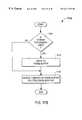
- the process 1700 Cdetermines if there is a next video stream (Block 1730 ). If YES, the VP de-interlaces the image (Block 1732 ). Then the process 1700 C writes the de-interlaced image data into the frame buffer in the memory at the specified location (Block 1734 ). The process 1700 C then comes back to block 1730 to determine if there are any more video streams.
- the process 1700 Cdisplays the content of the frame buffer on a television monitor.
- the content of the frame buffermay include results from other scaling and/or de-interlacing operations. The process 1700 C is then terminated.
- the present inventionis a technique to perform graphic and video operations effectively.
- the techniqueprovides an architecture that performs horizontal and vertical filtering, and de-interlacing on the image data.
- the filtering operationsperform down scaling and up scaling on patches of image data.
- On-chip buffersprovide fast and efficient memory accesses. Format conversion is performed as a series of steps including scaling and/or de-interlacing.
- the techniqueincludes up-scaling and down-scaling in horizontal and vertical directions using horizontal and vertical filters.
- the horizontal up-scalingis performed by an in-line multi-tap horizontal filter.
- the vertical up-scalingis performed by an in-line multi-tap vertical interpolator.
- the horizontal down-scalingis performed by a patch-based horizontal band-limiting filter and interpolator.
- the vertical down-scalingis performed by a patch-based vertical band-limiting filter and interpolator.
- the techniqueincludes the use of patches and scaling filters to convert from any input resolutions and scanning modes to any output resolutions and scanning modes.
- the patchesare transferred from memory to local buffers for filtering.
- the image data from the patchesare appropriately steered or organized/re-organized according to the image data organization.
- the techniqueincludes use of patches and motion detecting and interpolating.
- the patchesare transferred from memory to local buffers for de-interlacing.
- the image data from the patchesare appropriately steered or organized/re-organized according to the image data organization.
- the objectsare written to the display using patches in any order to achieve the desired results. Patches are written to a frame memory to be displayed on a monitor. A number of results can be achieved including overlapping, separating, animating, cinematic, etc.
Landscapes
- Engineering & Computer Science (AREA)
- Multimedia (AREA)
- Signal Processing (AREA)
- Physics & Mathematics (AREA)
- General Physics & Mathematics (AREA)
- Theoretical Computer Science (AREA)
- Computer Graphics (AREA)
- Computer Hardware Design (AREA)
- Software Systems (AREA)
- Business, Economics & Management (AREA)
- Marketing (AREA)
- Television Systems (AREA)
Abstract
Description
Claims (13)
Priority Applications (1)
| Application Number | Priority Date | Filing Date | Title |
|---|---|---|---|
| US09/285,490US6411333B1 (en) | 1999-04-02 | 1999-04-02 | Format conversion using patch-based filtering |
Applications Claiming Priority (1)
| Application Number | Priority Date | Filing Date | Title |
|---|---|---|---|
| US09/285,490US6411333B1 (en) | 1999-04-02 | 1999-04-02 | Format conversion using patch-based filtering |
Publications (1)
| Publication Number | Publication Date |
|---|---|
| US6411333B1true US6411333B1 (en) | 2002-06-25 |
Family
ID=23094466
Family Applications (1)
| Application Number | Title | Priority Date | Filing Date |
|---|---|---|---|
| US09/285,490Expired - LifetimeUS6411333B1 (en) | 1999-04-02 | 1999-04-02 | Format conversion using patch-based filtering |
Country Status (1)
| Country | Link |
|---|---|
| US (1) | US6411333B1 (en) |
Cited By (64)
| Publication number | Priority date | Publication date | Assignee | Title |
|---|---|---|---|---|
| US20020080268A1 (en)* | 2000-12-22 | 2002-06-27 | Willis Donald Henry | Method and system for MPEG chroma de-interlacing |
| US20020079989A1 (en)* | 2000-11-02 | 2002-06-27 | Michio Kadota | End surface reflection type surface acoustic wave apparatus |
| US20020106018A1 (en)* | 2001-02-05 | 2002-08-08 | D'luna Lionel | Single chip set-top box system |
| US20020172434A1 (en)* | 2001-04-20 | 2002-11-21 | Mitsubishi Electric Research Laboratories, Inc. | One-pass super-resolution images |
| US20020180883A1 (en)* | 2001-04-27 | 2002-12-05 | Kazunari Tomizawa | Image processing circuit, image display device, and an image processing method |
| US6529935B1 (en) | 1998-11-09 | 2003-03-04 | Broadcom Corporation | Graphics display system with unified memory architecture |
| US6538656B1 (en) | 1999-11-09 | 2003-03-25 | Broadcom Corporation | Video and graphics system with a data transport processor |
| US6545719B1 (en)* | 2000-03-31 | 2003-04-08 | Matsushita Electric Industrial Co., Ltd. | Apparatus and method for concealing interpolation artifacts in a video interlaced to progressive scan converter |
| US20030095203A1 (en)* | 2001-11-21 | 2003-05-22 | Macinnis Alexander G. | System and method for aligned compression of interlaced video |
| US6573905B1 (en) | 1999-11-09 | 2003-06-03 | Broadcom Corporation | Video and graphics system with parallel processing of graphics windows |
| US6628827B1 (en)* | 1999-12-14 | 2003-09-30 | Intel Corporation | Method of upscaling a color image |
| US20030185305A1 (en)* | 2002-04-01 | 2003-10-02 | Macinnis Alexander G. | Method of communicating between modules in a decoding system |
| US20030189581A1 (en)* | 2002-04-08 | 2003-10-09 | Nasoff David G. | Content based window filtering for simultaneous display of multiple high-quality video and graphics windows |
| US6636222B1 (en) | 1999-11-09 | 2003-10-21 | Broadcom Corporation | Video and graphics system with an MPEG video decoder for concurrent multi-row decoding |
| US6658399B1 (en)* | 1999-09-10 | 2003-12-02 | Intel Corporation | Fuzzy based thresholding technique for image segmentation |
| US6661422B1 (en) | 1998-11-09 | 2003-12-09 | Broadcom Corporation | Video and graphics system with MPEG specific data transfer commands |
| US20040028141A1 (en)* | 1999-11-09 | 2004-02-12 | Vivian Hsiun | Video decoding system having a programmable variable-length decoder |
| US6714256B2 (en)* | 1999-12-23 | 2004-03-30 | Harman Becker Automotive Systems Gmbh | Video signal processing system |
| US20040075768A1 (en)* | 2002-10-22 | 2004-04-22 | Patrick Law | Filter module for a video decoding system |
| US6768774B1 (en) | 1998-11-09 | 2004-07-27 | Broadcom Corporation | Video and graphics system with video scaling |
| US6798420B1 (en)* | 1998-11-09 | 2004-09-28 | Broadcom Corporation | Video and graphics system with a single-port RAM |
| US20040218834A1 (en)* | 2003-04-30 | 2004-11-04 | Microsoft Corporation | Patch-based video super-resolution |
| US6853385B1 (en) | 1999-11-09 | 2005-02-08 | Broadcom Corporation | Video, audio and graphics decode, composite and display system |
| US20050111752A1 (en)* | 2003-10-15 | 2005-05-26 | Stmicroelectronics S.A. | Image adapter with tilewise image processing, and method using such an adapter |
| US6937291B1 (en)* | 2000-08-31 | 2005-08-30 | Intel Corporation | Adaptive video scaler |
| US20050219409A1 (en)* | 2004-04-02 | 2005-10-06 | Kun-Nan Cheng | Display controlling device capable of displaying multi-windows and related method |
| US6975324B1 (en) | 1999-11-09 | 2005-12-13 | Broadcom Corporation | Video and graphics system with a video transport processor |
| US20060001774A1 (en)* | 2004-06-30 | 2006-01-05 | Kabushiki Kaisha Toshiba | Apparatus and method for processing video signal |
| US20060007200A1 (en)* | 2004-07-08 | 2006-01-12 | David Young | Method and system for displaying a sequence of image frames |
| US20060028581A1 (en)* | 2000-02-24 | 2006-02-09 | Tetsujiro Kondo | Image signal conversion apparatus, image signal conversion method, image display apparatus using the same and coefficient data generating apparatus used therein |
| US20060077213A1 (en)* | 2004-09-30 | 2006-04-13 | Chrontel, Inc. | Video conversion system and method |
| US20060132647A1 (en)* | 2004-12-22 | 2006-06-22 | Ming-Jane Hsieh | Method and apparatus for simultaneous display in progressive and interlaced scanning modes |
| US20060291751A1 (en)* | 2004-12-16 | 2006-12-28 | Peyman Milanfar | Robust reconstruction of high resolution grayscale images from a sequence of low-resolution frames (robust gray super-resolution) |
| US20060291750A1 (en)* | 2004-12-16 | 2006-12-28 | Peyman Milanfar | Dynamic reconstruction of high resolution video from low-resolution color-filtered video (video-to-video super-resolution) |
| US7158178B1 (en)* | 1999-12-14 | 2007-01-02 | Intel Corporation | Method of converting a sub-sampled color image |
| US20070030276A1 (en)* | 1998-11-09 | 2007-02-08 | Macinnis Alexander G | Video and graphics system with parallel processing of graphics windows |
| US20070041663A1 (en)* | 2005-08-03 | 2007-02-22 | Samsung Electronics Co., Ltd. | Apparatus and method for super-resolution enhancement processing |
| US20070222891A1 (en)* | 2006-03-21 | 2007-09-27 | Mediatek Inc. | Systems and methods for video data conversion |
| US20080036906A1 (en)* | 2002-07-23 | 2008-02-14 | Mediostream, Inc. | Method and system for direct recording of video information onto a disk medium |
| US20080043141A1 (en)* | 2006-06-30 | 2008-02-21 | Kabushiki Kaisha Toshiba | Video signal scaling apparatus |
| US7366491B1 (en)* | 1999-06-29 | 2008-04-29 | Sanyo Electric Co., Ltd. | Noise cancel circuit |
| US7446773B1 (en)* | 2004-12-14 | 2008-11-04 | Nvidia Corporation | Apparatus, system, and method for integrated heterogeneous processors with integrated scheduler |
| US7466316B1 (en) | 2004-12-14 | 2008-12-16 | Nvidia Corporation | Apparatus, system, and method for distributing work to integrated heterogeneous processors |
| US20090038588A1 (en)* | 2007-08-10 | 2009-02-12 | Nissan Motor Co., Ltd. | Variable compression ratio device for internal combustion engine |
| JPWO2007029323A1 (en)* | 2005-09-08 | 2009-03-12 | 三菱電機株式会社 | Rendering display device |
| US20090143884A1 (en)* | 2003-03-21 | 2009-06-04 | Intersil Americas Inc. | Systems and methods for sample rate conversion |
| US20090303156A1 (en)* | 2008-02-27 | 2009-12-10 | Subir Ghosh | System and method for low bandwidth display information transport |
| US7667710B2 (en) | 2003-04-25 | 2010-02-23 | Broadcom Corporation | Graphics display system with line buffer control scheme |
| US7738613B1 (en) | 2003-03-21 | 2010-06-15 | D2Audio Corporation | Streaming multi-channel audio as packetized data or parallel data with a separate input frame sync |
| US7898545B1 (en) | 2004-12-14 | 2011-03-01 | Nvidia Corporation | Apparatus, system, and method for integrated heterogeneous processors |
| US7908306B1 (en)* | 2003-03-21 | 2011-03-15 | D2Audio Corp | SRC with multiple sets of filter coefficients in memory and a high order coefficient interpolator |
| US7929718B1 (en) | 2003-05-12 | 2011-04-19 | D2Audio Corporation | Systems and methods for switching and mixing signals in a multi-channel amplifier |
| US20110109794A1 (en)* | 2009-11-06 | 2011-05-12 | Paul Wiercienski | Caching structure and apparatus for use in block based video |
| US8063916B2 (en) | 2003-10-22 | 2011-11-22 | Broadcom Corporation | Graphics layer reduction for video composition |
| WO2012054720A1 (en)* | 2010-10-20 | 2012-04-26 | Ncomputing Inc. | System and method for downsizing video data for memory bandwidth optimization |
| US8199154B2 (en) | 1998-11-09 | 2012-06-12 | Broadcom Corporation | Low resolution graphics mode support using window descriptors |
| US8749566B2 (en) | 2010-11-16 | 2014-06-10 | Ncomputing Inc. | System and method for an optimized on-the-fly table creation algorithm |
| US8896612B2 (en) | 2010-11-16 | 2014-11-25 | Ncomputing Inc. | System and method for on-the-fly key color generation |
| WO2017142851A1 (en)* | 2016-02-19 | 2017-08-24 | Micron Technology, Inc. | Modified decode for corner turn |
| US20170359586A1 (en)* | 2016-06-10 | 2017-12-14 | Apple Inc. | Transcoding techniques for alternate displays |
| US9892767B2 (en) | 2016-02-12 | 2018-02-13 | Micron Technology, Inc. | Data gathering in memory |
| US9990967B2 (en) | 2016-04-20 | 2018-06-05 | Micron Technology, Inc. | Apparatuses and methods for performing corner turn operations using sensing circuitry |
| US10153008B2 (en) | 2016-04-20 | 2018-12-11 | Micron Technology, Inc. | Apparatuses and methods for performing corner turn operations using sensing circuitry |
| US12165278B2 (en)* | 2020-09-18 | 2024-12-10 | Imagination Technologies Limited | Downscaler and method of downscaling |
Citations (15)
| Publication number | Priority date | Publication date | Assignee | Title |
|---|---|---|---|---|
| US5781241A (en)* | 1996-11-08 | 1998-07-14 | Chrontel, Inc. | Apparatus and method to convert computer graphics signals to television video signals with vertical and horizontal scaling requiring no frame buffers |
| US5861864A (en)* | 1996-04-02 | 1999-01-19 | Hewlett-Packard Company | Video interface system and method |
| US5874937A (en)* | 1995-10-20 | 1999-02-23 | Seiko Epson Corporation | Method and apparatus for scaling up and down a video image |
| US5917549A (en)* | 1996-08-07 | 1999-06-29 | Adobe Systems Incorporated | Transforming images with different pixel aspect ratios |
| US5943097A (en)* | 1993-12-24 | 1999-08-24 | Canon Kabushiki Kaisha | Image processing means for processing image signals of different signal formats |
| US5982443A (en)* | 1997-04-19 | 1999-11-09 | Hyundai Electronics Industries Co., Ltd. | Apparatus and method for converting scan format of video signal |
| US6037986A (en)* | 1996-07-16 | 2000-03-14 | Divicom Inc. | Video preprocessing method and apparatus with selective filtering based on motion detection |
| US6091426A (en)* | 1995-04-07 | 2000-07-18 | Intel Corporation | Integrating data scaling and buffering functions to minimize memory requirement |
| US6108047A (en)* | 1997-10-28 | 2000-08-22 | Stream Machine Company | Variable-size spatial and temporal video scaler |
| US6118486A (en)* | 1997-09-26 | 2000-09-12 | Sarnoff Corporation | Synchronized multiple format video processing method and apparatus |
| US6144412A (en)* | 1996-10-15 | 2000-11-07 | Hitachi, Ltd. | Method and circuit for signal processing of format conversion of picture signal |
| US6226038B1 (en)* | 1998-04-03 | 2001-05-01 | Avid Technology, Inc. | HDTV editing and effects previsualization using SDTV devices |
| US6229571B1 (en)* | 1998-07-23 | 2001-05-08 | Nec Corporation | Scan converter with interpolating function |
| US6239847B1 (en)* | 1997-12-15 | 2001-05-29 | Netergy Networks, Inc. | Two pass multi-dimensional data scaling arrangement and method thereof |
| US6256068B1 (en)* | 1996-05-08 | 2001-07-03 | Matsushita Electric Industrial Co., Ltd. | Image data format conversion apparatus |
- 1999
- 1999-04-02USUS09/285,490patent/US6411333B1/ennot_activeExpired - Lifetime
Patent Citations (16)
| Publication number | Priority date | Publication date | Assignee | Title |
|---|---|---|---|---|
| US5943097A (en)* | 1993-12-24 | 1999-08-24 | Canon Kabushiki Kaisha | Image processing means for processing image signals of different signal formats |
| US6091426A (en)* | 1995-04-07 | 2000-07-18 | Intel Corporation | Integrating data scaling and buffering functions to minimize memory requirement |
| US5874937A (en)* | 1995-10-20 | 1999-02-23 | Seiko Epson Corporation | Method and apparatus for scaling up and down a video image |
| US5861864A (en)* | 1996-04-02 | 1999-01-19 | Hewlett-Packard Company | Video interface system and method |
| US6256068B1 (en)* | 1996-05-08 | 2001-07-03 | Matsushita Electric Industrial Co., Ltd. | Image data format conversion apparatus |
| US6037986A (en)* | 1996-07-16 | 2000-03-14 | Divicom Inc. | Video preprocessing method and apparatus with selective filtering based on motion detection |
| US5917549A (en)* | 1996-08-07 | 1999-06-29 | Adobe Systems Incorporated | Transforming images with different pixel aspect ratios |
| US6144412A (en)* | 1996-10-15 | 2000-11-07 | Hitachi, Ltd. | Method and circuit for signal processing of format conversion of picture signal |
| US5781241A (en)* | 1996-11-08 | 1998-07-14 | Chrontel, Inc. | Apparatus and method to convert computer graphics signals to television video signals with vertical and horizontal scaling requiring no frame buffers |
| US5914753A (en)* | 1996-11-08 | 1999-06-22 | Chrontel, Inc. | Apparatus and method to convert computer graphics signals to television video signals with vertical and horizontal scaling requiring no frame buffers |
| US5982443A (en)* | 1997-04-19 | 1999-11-09 | Hyundai Electronics Industries Co., Ltd. | Apparatus and method for converting scan format of video signal |
| US6118486A (en)* | 1997-09-26 | 2000-09-12 | Sarnoff Corporation | Synchronized multiple format video processing method and apparatus |
| US6108047A (en)* | 1997-10-28 | 2000-08-22 | Stream Machine Company | Variable-size spatial and temporal video scaler |
| US6239847B1 (en)* | 1997-12-15 | 2001-05-29 | Netergy Networks, Inc. | Two pass multi-dimensional data scaling arrangement and method thereof |
| US6226038B1 (en)* | 1998-04-03 | 2001-05-01 | Avid Technology, Inc. | HDTV editing and effects previsualization using SDTV devices |
| US6229571B1 (en)* | 1998-07-23 | 2001-05-08 | Nec Corporation | Scan converter with interpolating function |
Cited By (165)
| Publication number | Priority date | Publication date | Assignee | Title |
|---|---|---|---|---|
| US6738072B1 (en) | 1998-11-09 | 2004-05-18 | Broadcom Corporation | Graphics display system with anti-flutter filtering and vertical scaling feature |
| US8848792B2 (en) | 1998-11-09 | 2014-09-30 | Broadcom Corporation | Video and graphics system with video scaling |
| US7554553B2 (en) | 1998-11-09 | 2009-06-30 | Broadcom Corporation | Graphics display system with anti-flutter filtering and vertical scaling feature |
| US7538783B2 (en) | 1998-11-09 | 2009-05-26 | Broadcom Corporation | Graphics display system with video scaler |
| US7530027B2 (en) | 1998-11-09 | 2009-05-05 | Broadcom Corporation | Graphics display system with graphics window control mechanism |
| US6529935B1 (en) | 1998-11-09 | 2003-03-04 | Broadcom Corporation | Graphics display system with unified memory architecture |
| US7598962B2 (en) | 1998-11-09 | 2009-10-06 | Broadcom Corporation | Graphics display system with window descriptors |
| US7659900B2 (en) | 1998-11-09 | 2010-02-09 | Broadcom Corporation | Video and graphics system with parallel processing of graphics windows |
| US7746354B2 (en) | 1998-11-09 | 2010-06-29 | Broadcom Corporation | Graphics display system with anti-aliased text and graphics feature |
| US7920151B2 (en) | 1998-11-09 | 2011-04-05 | Broadcom Corporation | Graphics display system with video scaler |
| US7446774B1 (en) | 1998-11-09 | 2008-11-04 | Broadcom Corporation | Video and graphics system with an integrated system bridge controller |
| US6608630B1 (en) | 1998-11-09 | 2003-08-19 | Broadcom Corporation | Graphics display system with line buffer control scheme |
| US7365752B2 (en) | 1998-11-09 | 2008-04-29 | Broadcom Corporation | Video and graphics system with a single-port RAM |
| US7015928B2 (en) | 1998-11-09 | 2006-03-21 | Broadcom Corporation | Graphics display system with color look-up table loading mechanism |
| US6630945B1 (en) | 1998-11-09 | 2003-10-07 | Broadcom Corporation | Graphics display system with graphics window control mechanism |
| US7911483B1 (en) | 1998-11-09 | 2011-03-22 | Broadcom Corporation | Graphics display system with window soft horizontal scrolling mechanism |
| US7310104B2 (en) | 1998-11-09 | 2007-12-18 | Broadcom Corporation | Graphics display system with anti-flutter filtering and vertical scaling feature |
| US7057622B2 (en) | 1998-11-09 | 2006-06-06 | Broadcom Corporation | Graphics display system with line buffer control scheme |
| US6661422B1 (en) | 1998-11-09 | 2003-12-09 | Broadcom Corporation | Video and graphics system with MPEG specific data transfer commands |
| US6661427B1 (en)* | 1998-11-09 | 2003-12-09 | Broadcom Corporation | Graphics display system with video scaler |
| US20070285440A1 (en)* | 1998-11-09 | 2007-12-13 | Macinnis Alexander G | Graphics display system with video synchronization feature |
| US6700588B1 (en) | 1998-11-09 | 2004-03-02 | Broadcom Corporation | Apparatus and method for blending graphics and video surfaces |
| US7277099B2 (en) | 1998-11-09 | 2007-10-02 | Broadcom Corporation | Video and graphics system with an MPEG video decoder for concurrent multi-row decoding |
| US6721837B2 (en) | 1998-11-09 | 2004-04-13 | Broadcom Corporation | Graphics display system with unified memory architecture |
| US9575665B2 (en) | 1998-11-09 | 2017-02-21 | Broadcom Corporation | Graphics display system with unified memory architecture |
| US6731295B1 (en) | 1998-11-09 | 2004-05-04 | Broadcom Corporation | Graphics display system with window descriptors |
| US7545438B2 (en) | 1998-11-09 | 2009-06-09 | Broadcom Corporation | Graphics display system with video synchronization feature |
| US8493415B2 (en) | 1998-11-09 | 2013-07-23 | Broadcom Corporation | Graphics display system with video scaler |
| US6570579B1 (en) | 1998-11-09 | 2003-05-27 | Broadcom Corporation | Graphics display system |
| US6768774B1 (en) | 1998-11-09 | 2004-07-27 | Broadcom Corporation | Video and graphics system with video scaling |
| US20040150652A1 (en)* | 1998-11-09 | 2004-08-05 | Broadcom Corporation | Graphics display system with window descriptors |
| US7256790B2 (en) | 1998-11-09 | 2007-08-14 | Broadcom Corporation | Video and graphics system with MPEG specific data transfer commands |
| US6798420B1 (en)* | 1998-11-09 | 2004-09-28 | Broadcom Corporation | Video and graphics system with a single-port RAM |
| US9111369B2 (en) | 1998-11-09 | 2015-08-18 | Broadcom Corporation | Graphics accelerator |
| US6819330B2 (en) | 1998-11-09 | 2004-11-16 | Broadcom Corporation | Graphics display System with color look-up table loading mechanism |
| US20040246257A1 (en)* | 1998-11-09 | 2004-12-09 | Macinnis Alexander G. | Graphics accelerator |
| US7227582B2 (en) | 1998-11-09 | 2007-06-05 | Broadcom Corporation | Graphics display system with video synchronization feature |
| US7184058B2 (en) | 1998-11-09 | 2007-02-27 | Broadcom Corporation | Graphics display system with anti-aliased text and graphics feature |
| US7991049B2 (en) | 1998-11-09 | 2011-08-02 | Broadcom Corporation | Video and graphics system with video scaling |
| US20070030276A1 (en)* | 1998-11-09 | 2007-02-08 | Macinnis Alexander G | Video and graphics system with parallel processing of graphics windows |
| US6879330B2 (en) | 1998-11-09 | 2005-04-12 | Broadcom Corporation | Graphics display system with anti-flutter filtering and vertical scaling feature |
| US9077997B2 (en) | 1998-11-09 | 2015-07-07 | Broadcom Corporation | Graphics display system with unified memory architecture |
| US20110193868A1 (en)* | 1998-11-09 | 2011-08-11 | Broadcom Corporation | Graphics accelerator |
| US6927783B1 (en) | 1998-11-09 | 2005-08-09 | Broadcom Corporation | Graphics display system with anti-aliased text and graphics feature |
| US8199154B2 (en) | 1998-11-09 | 2012-06-12 | Broadcom Corporation | Low resolution graphics mode support using window descriptors |
| US7110006B2 (en) | 1998-11-09 | 2006-09-19 | Broadcom Corporation | Video, audio and graphics decode, composite and display system |
| US7098930B2 (en) | 1998-11-09 | 2006-08-29 | Broadcom Corporation | Graphics display system with anti-flutter filtering and vertical scaling feature |
| US7554562B2 (en) | 1998-11-09 | 2009-06-30 | Broadcom Corporation | Graphics display system with anti-flutter filtering and vertical scaling feature |
| US6744472B1 (en) | 1998-11-09 | 2004-06-01 | Broadcom Corporation | Graphics display system with video synchronization feature |
| US7071944B2 (en) | 1998-11-09 | 2006-07-04 | Broadcom Corporation | Video and graphics system with parallel processing of graphics windows |
| US8390635B2 (en) | 1998-11-09 | 2013-03-05 | Broadcom Corporation | Graphics accelerator |
| US7002602B2 (en) | 1998-11-09 | 2006-02-21 | Broadcom Corporation | Apparatus and method for blending graphics and video surfaces |
| US7366491B1 (en)* | 1999-06-29 | 2008-04-29 | Sanyo Electric Co., Ltd. | Noise cancel circuit |
| US6658399B1 (en)* | 1999-09-10 | 2003-12-02 | Intel Corporation | Fuzzy based thresholding technique for image segmentation |
| US6975324B1 (en) | 1999-11-09 | 2005-12-13 | Broadcom Corporation | Video and graphics system with a video transport processor |
| US6573905B1 (en) | 1999-11-09 | 2003-06-03 | Broadcom Corporation | Video and graphics system with parallel processing of graphics windows |
| US20040028141A1 (en)* | 1999-11-09 | 2004-02-12 | Vivian Hsiun | Video decoding system having a programmable variable-length decoder |
| US6636222B1 (en) | 1999-11-09 | 2003-10-21 | Broadcom Corporation | Video and graphics system with an MPEG video decoder for concurrent multi-row decoding |
| US6781601B2 (en) | 1999-11-09 | 2004-08-24 | Broadcom Corporation | Transport processor |
| US6538656B1 (en) | 1999-11-09 | 2003-03-25 | Broadcom Corporation | Video and graphics system with a data transport processor |
| US6853385B1 (en) | 1999-11-09 | 2005-02-08 | Broadcom Corporation | Video, audio and graphics decode, composite and display system |
| US7667715B2 (en) | 1999-11-09 | 2010-02-23 | Broadcom Corporation | Video, audio and graphics decode, composite and display system |
| US8913667B2 (en) | 1999-11-09 | 2014-12-16 | Broadcom Corporation | Video decoding system having a programmable variable-length decoder |
| US20060268012A1 (en)* | 1999-11-09 | 2006-11-30 | Macinnis Alexander G | Video, audio and graphics decode, composite and display system |
| US20050044175A1 (en)* | 1999-11-09 | 2005-02-24 | Francis Cheung | Transport processor |
| US7848430B2 (en) | 1999-11-09 | 2010-12-07 | Broadcom Corporation | Video and graphics system with an MPEG video decoder for concurrent multi-row decoding |
| US6870538B2 (en) | 1999-11-09 | 2005-03-22 | Broadcom Corporation | Video and graphics system with parallel processing of graphics windows |
| US7158178B1 (en)* | 1999-12-14 | 2007-01-02 | Intel Corporation | Method of converting a sub-sampled color image |
| US6628827B1 (en)* | 1999-12-14 | 2003-09-30 | Intel Corporation | Method of upscaling a color image |
| US6714256B2 (en)* | 1999-12-23 | 2004-03-30 | Harman Becker Automotive Systems Gmbh | Video signal processing system |
| US7227584B2 (en) | 1999-12-23 | 2007-06-05 | Harman Becker Automotive Systems Gmbh | Video signal processing system |
| US20040263691A1 (en)* | 1999-12-23 | 2004-12-30 | Bernd Broghammer | Video signal processing system |
| US20060028581A1 (en)* | 2000-02-24 | 2006-02-09 | Tetsujiro Kondo | Image signal conversion apparatus, image signal conversion method, image display apparatus using the same and coefficient data generating apparatus used therein |
| US7551226B2 (en)* | 2000-02-24 | 2009-06-23 | Sony Corporation | Image signal conversion apparatus, method and, display for image signal conversion based on selected pixel data |
| US6545719B1 (en)* | 2000-03-31 | 2003-04-08 | Matsushita Electric Industrial Co., Ltd. | Apparatus and method for concealing interpolation artifacts in a video interlaced to progressive scan converter |
| US6937291B1 (en)* | 2000-08-31 | 2005-08-30 | Intel Corporation | Adaptive video scaler |
| US20020079989A1 (en)* | 2000-11-02 | 2002-06-27 | Michio Kadota | End surface reflection type surface acoustic wave apparatus |
| US20020080268A1 (en)* | 2000-12-22 | 2002-06-27 | Willis Donald Henry | Method and system for MPEG chroma de-interlacing |
| US20060077293A1 (en)* | 2000-12-22 | 2006-04-13 | Willis Donald H | Method and system for MPEG chroma de-interlacing |
| US7006147B2 (en)* | 2000-12-22 | 2006-02-28 | Thomson Lincensing | Method and system for MPEG chroma de-interlacing |
| US7728907B2 (en) | 2000-12-22 | 2010-06-01 | Thomson Licensing | Method and system for MPEG chroma de-interlacing |
| US20020106018A1 (en)* | 2001-02-05 | 2002-08-08 | D'luna Lionel | Single chip set-top box system |
| US9668011B2 (en) | 2001-02-05 | 2017-05-30 | Avago Technologies General Ip (Singapore) Pte. Ltd. | Single chip set-top box system |
| US20020172434A1 (en)* | 2001-04-20 | 2002-11-21 | Mitsubishi Electric Research Laboratories, Inc. | One-pass super-resolution images |
| US6766067B2 (en)* | 2001-04-20 | 2004-07-20 | Mitsubishi Electric Research Laboratories, Inc. | One-pass super-resolution images |
| US20060187343A1 (en)* | 2001-04-27 | 2006-08-24 | Kazunari Tomizawa | Image processing circuit, image display device, and an image processing method |
| US20110141370A1 (en)* | 2001-04-27 | 2011-06-16 | Kazunari Tomizawa | Image processing circuit, image display device, and an image processing method |
| US7408588B2 (en) | 2001-04-27 | 2008-08-05 | Shapr Kabushiki Kaisha | Image processing circuit, image display device, and an image processing method |
| US20070159554A1 (en)* | 2001-04-27 | 2007-07-12 | Kazunari Tomizawa | Image processing circuit, image display device, and an image processing method |
| US8502917B2 (en) | 2001-04-27 | 2013-08-06 | Sharp Kabushiki Kaisha | Image processing circuit, image display device, and an image processing method |
| US20020180883A1 (en)* | 2001-04-27 | 2002-12-05 | Kazunari Tomizawa | Image processing circuit, image display device, and an image processing method |
| US7916213B2 (en) | 2001-04-27 | 2011-03-29 | Sharp Kabushiki Kaisha | Image processing circuit, image display device, and an image processing method |
| US7068320B2 (en)* | 2001-04-27 | 2006-06-27 | Sharp Kabushiki Kaisha | Image processing circuit, image display device, and an image processing method |
| US20030095203A1 (en)* | 2001-11-21 | 2003-05-22 | Macinnis Alexander G. | System and method for aligned compression of interlaced video |
| US7262806B2 (en)* | 2001-11-21 | 2007-08-28 | Broadcom Corporation | System and method for aligned compression of interlaced video |
| US6963613B2 (en)* | 2002-04-01 | 2005-11-08 | Broadcom Corporation | Method of communicating between modules in a decoding system |
| US20030185305A1 (en)* | 2002-04-01 | 2003-10-02 | Macinnis Alexander G. | Method of communicating between modules in a decoding system |
| EP1353321A3 (en)* | 2002-04-08 | 2005-07-13 | Matsushita Electric Industrial Co., Ltd. | Content based window filtering for simultaneous display of multiple high-quality video and graphics windows |
| US20030189581A1 (en)* | 2002-04-08 | 2003-10-09 | Nasoff David G. | Content based window filtering for simultaneous display of multiple high-quality video and graphics windows |
| US8619188B2 (en) | 2002-07-23 | 2013-12-31 | Mediostream, Inc. | Method and system for direct recording of video information onto a disk medium |
| US20110044661A1 (en)* | 2002-07-23 | 2011-02-24 | Mediostream, Inc. | Method and system for direct recording of video information onto a disk medium |
| US7843508B2 (en) | 2002-07-23 | 2010-11-30 | Mediostream, Inc. | Method and system for direct recording of video information onto a disk medium |
| US20080036906A1 (en)* | 2002-07-23 | 2008-02-14 | Mediostream, Inc. | Method and system for direct recording of video information onto a disk medium |
| US20040075768A1 (en)* | 2002-10-22 | 2004-04-22 | Patrick Law | Filter module for a video decoding system |
| US7636125B2 (en)* | 2002-10-22 | 2009-12-22 | Broadcom Corporation | Filter module for a video decoding system |
| US8085346B2 (en)* | 2002-10-22 | 2011-12-27 | Broadcom Corporation | Filter module for a video decoding system |
| US8619191B2 (en)* | 2002-10-22 | 2013-12-31 | Broadcom Corporation | Filter module for a video decoding system |
| US20100066902A1 (en)* | 2002-10-22 | 2010-03-18 | Patrick Law | Filter module for a video decoding system |
| US7738613B1 (en) | 2003-03-21 | 2010-06-15 | D2Audio Corporation | Streaming multi-channel audio as packetized data or parallel data with a separate input frame sync |
| US7970088B2 (en) | 2003-03-21 | 2011-06-28 | Intersil Americas Inc. | Systems and methods for sample rate conversion |
| US20090143884A1 (en)* | 2003-03-21 | 2009-06-04 | Intersil Americas Inc. | Systems and methods for sample rate conversion |
| US7908306B1 (en)* | 2003-03-21 | 2011-03-15 | D2Audio Corp | SRC with multiple sets of filter coefficients in memory and a high order coefficient interpolator |
| US7667710B2 (en) | 2003-04-25 | 2010-02-23 | Broadcom Corporation | Graphics display system with line buffer control scheme |
| US20040218834A1 (en)* | 2003-04-30 | 2004-11-04 | Microsoft Corporation | Patch-based video super-resolution |
| US7218796B2 (en)* | 2003-04-30 | 2007-05-15 | Microsoft Corporation | Patch-based video super-resolution |
| US7929718B1 (en) | 2003-05-12 | 2011-04-19 | D2Audio Corporation | Systems and methods for switching and mixing signals in a multi-channel amplifier |
| US7551803B2 (en)* | 2003-10-15 | 2009-06-23 | Stmicroelectronics S.A. | Image adapter with tilewise image processing, and method using such an adapter |
| US20050111752A1 (en)* | 2003-10-15 | 2005-05-26 | Stmicroelectronics S.A. | Image adapter with tilewise image processing, and method using such an adapter |
| US20090226115A1 (en)* | 2003-10-15 | 2009-09-10 | Stmicroelectronics S.A. | Image adapter with tilewise image processing, and method using such an adapter |
| US7925119B2 (en) | 2003-10-15 | 2011-04-12 | Stmicroelectronics S.A. | Image adapter with tilewise image processing, and method using such an adapter |
| US8063916B2 (en) | 2003-10-22 | 2011-11-22 | Broadcom Corporation | Graphics layer reduction for video composition |
| US20050219409A1 (en)* | 2004-04-02 | 2005-10-06 | Kun-Nan Cheng | Display controlling device capable of displaying multi-windows and related method |
| US7463307B2 (en)* | 2004-04-02 | 2008-12-09 | Mstar Semiconductor, Inc. | Display controlling device capable of displaying multi-windows and related method |
| US20060001774A1 (en)* | 2004-06-30 | 2006-01-05 | Kabushiki Kaisha Toshiba | Apparatus and method for processing video signal |
| US7492380B2 (en)* | 2004-06-30 | 2009-02-17 | Kabushiki Kaisha Toshiba | Apparatus and method for processing video signal |
| US20060007200A1 (en)* | 2004-07-08 | 2006-01-12 | David Young | Method and system for displaying a sequence of image frames |
| US20060077213A1 (en)* | 2004-09-30 | 2006-04-13 | Chrontel, Inc. | Video conversion system and method |
| US7446773B1 (en)* | 2004-12-14 | 2008-11-04 | Nvidia Corporation | Apparatus, system, and method for integrated heterogeneous processors with integrated scheduler |
| US7898545B1 (en) | 2004-12-14 | 2011-03-01 | Nvidia Corporation | Apparatus, system, and method for integrated heterogeneous processors |
| US7466316B1 (en) | 2004-12-14 | 2008-12-16 | Nvidia Corporation | Apparatus, system, and method for distributing work to integrated heterogeneous processors |
| US8203562B1 (en) | 2004-12-14 | 2012-06-19 | Nvidia Corporation | Apparatus, system, and method for distributing work to integrated heterogeneous processors |
| US20060291751A1 (en)* | 2004-12-16 | 2006-12-28 | Peyman Milanfar | Robust reconstruction of high resolution grayscale images from a sequence of low-resolution frames (robust gray super-resolution) |
| US20060291750A1 (en)* | 2004-12-16 | 2006-12-28 | Peyman Milanfar | Dynamic reconstruction of high resolution video from low-resolution color-filtered video (video-to-video super-resolution) |
| US20060132647A1 (en)* | 2004-12-22 | 2006-06-22 | Ming-Jane Hsieh | Method and apparatus for simultaneous display in progressive and interlaced scanning modes |
| US20070041663A1 (en)* | 2005-08-03 | 2007-02-22 | Samsung Electronics Co., Ltd. | Apparatus and method for super-resolution enhancement processing |
| US7715658B2 (en)* | 2005-08-03 | 2010-05-11 | Samsung Electronics Co., Ltd. | Apparatus and method for super-resolution enhancement processing |
| US20090289954A1 (en)* | 2005-09-08 | 2009-11-26 | Mitsubishi Electric Corporation | Rendering Display Device |
| JP4924427B2 (en)* | 2005-09-08 | 2012-04-25 | 三菱電機株式会社 | Rendering display device |
| EP1933299A4 (en)* | 2005-09-08 | 2010-03-03 | Mitsubishi Electric Corp | RENDER DISPLAY DEVICE |
| CN101427304B (en)* | 2005-09-08 | 2011-07-13 | 三菱电机株式会社 | Rendering display device |
| JPWO2007029323A1 (en)* | 2005-09-08 | 2009-03-12 | 三菱電機株式会社 | Rendering display device |
| US7724305B2 (en)* | 2006-03-21 | 2010-05-25 | Mediatek Inc. | Video data conversion method and system for multiple receivers |
| US20070222891A1 (en)* | 2006-03-21 | 2007-09-27 | Mediatek Inc. | Systems and methods for video data conversion |
| US20080043141A1 (en)* | 2006-06-30 | 2008-02-21 | Kabushiki Kaisha Toshiba | Video signal scaling apparatus |
| US20090038588A1 (en)* | 2007-08-10 | 2009-02-12 | Nissan Motor Co., Ltd. | Variable compression ratio device for internal combustion engine |
| US9161063B2 (en)* | 2008-02-27 | 2015-10-13 | Ncomputing, Inc. | System and method for low bandwidth display information transport |
| US9635373B2 (en) | 2008-02-27 | 2017-04-25 | Ncomputing, Inc. | System and method for low bandwidth display information transport |
| US20090303156A1 (en)* | 2008-02-27 | 2009-12-10 | Subir Ghosh | System and method for low bandwidth display information transport |
| US20110109794A1 (en)* | 2009-11-06 | 2011-05-12 | Paul Wiercienski | Caching structure and apparatus for use in block based video |
| WO2012054720A1 (en)* | 2010-10-20 | 2012-04-26 | Ncomputing Inc. | System and method for downsizing video data for memory bandwidth optimization |
| US8907987B2 (en) | 2010-10-20 | 2014-12-09 | Ncomputing Inc. | System and method for downsizing video data for memory bandwidth optimization |
| US8896612B2 (en) | 2010-11-16 | 2014-11-25 | Ncomputing Inc. | System and method for on-the-fly key color generation |
| US8749566B2 (en) | 2010-11-16 | 2014-06-10 | Ncomputing Inc. | System and method for an optimized on-the-fly table creation algorithm |
| US9892767B2 (en) | 2016-02-12 | 2018-02-13 | Micron Technology, Inc. | Data gathering in memory |
| US10026459B2 (en) | 2016-02-12 | 2018-07-17 | Micron Technology, Inc. | Data gathering in memory |
| WO2017142851A1 (en)* | 2016-02-19 | 2017-08-24 | Micron Technology, Inc. | Modified decode for corner turn |
| US10783942B2 (en) | 2016-02-19 | 2020-09-22 | Micron Technology, Inc. | Modified decode for corner turn |
| US9899070B2 (en) | 2016-02-19 | 2018-02-20 | Micron Technology, Inc. | Modified decode for corner turn |
| US10217499B2 (en) | 2016-02-19 | 2019-02-26 | Micron Technology, Inc. | Modified decode for corner turn |
| US10153008B2 (en) | 2016-04-20 | 2018-12-11 | Micron Technology, Inc. | Apparatuses and methods for performing corner turn operations using sensing circuitry |
| US9990967B2 (en) | 2016-04-20 | 2018-06-05 | Micron Technology, Inc. | Apparatuses and methods for performing corner turn operations using sensing circuitry |
| US10699756B2 (en) | 2016-04-20 | 2020-06-30 | Micron Technology, Inc. | Apparatuses and methods for performing corner turn operations using sensing circuitry |
| US10178394B2 (en)* | 2016-06-10 | 2019-01-08 | Apple Inc. | Transcoding techniques for alternate displays |
| US20170359586A1 (en)* | 2016-06-10 | 2017-12-14 | Apple Inc. | Transcoding techniques for alternate displays |
| US12165278B2 (en)* | 2020-09-18 | 2024-12-10 | Imagination Technologies Limited | Downscaler and method of downscaling |
Similar Documents
| Publication | Publication Date | Title |
|---|---|---|
| US6411333B1 (en) | Format conversion using patch-based filtering | |
| US6327000B1 (en) | Efficient image scaling for scan rate conversion | |
| US6556193B1 (en) | De-interlacing video images using patch-based processing | |
| US6539120B1 (en) | MPEG decoder providing multiple standard output signals | |
| EP0901734B1 (en) | Mpeg decoder providing multiple standard output signals | |
| US6456329B1 (en) | De-interlacing of video signals | |
| US6611260B1 (en) | Ultra-high bandwidth multi-port memory system for image scaling applications | |
| US5859651A (en) | Method and apparatus for block data transfer to reduce on-chip storage for interpolative video resizing | |
| EP1653735A1 (en) | Television receiver, video signal processing device, image processing method and device | |
| US6903733B1 (en) | Ultra-high bandwidth multi-port memory system for image scaling applications | |
| EP2337334B1 (en) | Shared memory multi video channel display apparatus and methods | |
| WO1998041012A9 (en) | Mpeg decoder providing multiple standard output signals | |
| US7719547B2 (en) | Video and graphics system with square graphics pixels | |
| US5977947A (en) | Method and apparatus for resizing block ordered video image frames with reduced on-chip cache | |
| JP2009534933A (en) | Shared memory multi-video channel display apparatus and method | |
| WO1997014247A1 (en) | Method and apparatus for video scaling and convolution for displaying computer graphics on a conventional television monitor | |
| US6259479B1 (en) | Letterbox filter apparatus and method | |
| US6563511B1 (en) | Anti-flickering for video display based on pixel luminance | |
| Jaspers et al. | Chip-set for video display of multimedia information | |
| US5668602A (en) | Real-time television image pixel multiplication methods and apparatus | |
| US6411334B1 (en) | Aspect ratio correction using digital filtering | |
| US7015975B2 (en) | Image processing device with a processing unit that processes image data in units of one scan line | |
| KR100463552B1 (en) | Cubic convolution interpolation apparatus and method | |
| Hsia et al. | A parallel video converter for displaying 4: 3 images on 16: 9 HDTV receivers | |
| Mizosoe et al. | An advanced multimedia processing LSI suitable for HDTV applications |
Legal Events
| Date | Code | Title | Description |
|---|---|---|---|
| AS | Assignment | Owner name:TERALOGIC, INC., CALIFORNIA Free format text:ASSIGNMENT OF ASSIGNORS INTEREST;ASSIGNORS:AULD, DAVID;YEH, GERARD K.;TRAJMAR, PETER;AND OTHERS;REEL/FRAME:010053/0897;SIGNING DATES FROM 19990518 TO 19990612 | |
| STCF | Information on status: patent grant | Free format text:PATENTED CASE | |
| AS | Assignment | Owner name:ORCLAND INC., NEW YORK Free format text:SECURITY INTEREST;ASSIGNOR:TERALOGIC, INC.;REEL/FRAME:013248/0398 Effective date:20020605 | |
| CC | Certificate of correction | ||
| FEPP | Fee payment procedure | Free format text:PAYOR NUMBER ASSIGNED (ORIGINAL EVENT CODE: ASPN); ENTITY STATUS OF PATENT OWNER: LARGE ENTITY | |
| AS | Assignment | Owner name:ZORAN CORPORATION, CALIFORNIA Free format text:ASSIGNMENT OF ASSIGNORS INTEREST;ASSIGNOR:TERALOGIC INC. BY THEIR DULY AUTHORIZED OFFICER, CHRIS DENTEN;REEL/FRAME:015394/0311 Effective date:20041106 | |
| FPAY | Fee payment | Year of fee payment:4 | |
| FEPP | Fee payment procedure | Free format text:PAYOR NUMBER ASSIGNED (ORIGINAL EVENT CODE: ASPN); ENTITY STATUS OF PATENT OWNER: LARGE ENTITY Free format text:PAYER NUMBER DE-ASSIGNED (ORIGINAL EVENT CODE: RMPN); ENTITY STATUS OF PATENT OWNER: LARGE ENTITY | |
| AS | Assignment | Owner name:TERALOGIC, INC., CALIFORNIA Free format text:RELEASE AND TERMINATION OF SECURITY INTEREST;ASSIGNOR:ORCLAND INC.;REEL/FRAME:022494/0738 Effective date:20090220 Owner name:ZORAN CORPORATION, CALIFORNIA Free format text:RELEASE AND TERMINATION OF SECURITY INTEREST;ASSIGNOR:ORCLAND INC.;REEL/FRAME:022494/0738 Effective date:20090220 | |
| AS | Assignment | Owner name:OAK TECHNOLOGY, INC., CALIFORNIA Free format text:AGREEMENT AND PLAN OF MERGER;ASSIGNOR:TERALOGIC, INC.;REEL/FRAME:023438/0116 Effective date:20021007 Owner name:OAK TECHNOLOGY, INC.,CALIFORNIA Free format text:AGREEMENT AND PLAN OF MERGER;ASSIGNOR:TERALOGIC, INC.;REEL/FRAME:023438/0116 Effective date:20021007 | |
| AS | Assignment | Owner name:TERALOGIC, INC., CALIFORNIA Free format text:MERGER;ASSIGNOR:OPTIC ACQUISITION CORP.;REEL/FRAME:023438/0579 Effective date:20021025 Owner name:TERALOGIC, INC.,CALIFORNIA Free format text:MERGER;ASSIGNOR:OPTIC ACQUISITION CORP.;REEL/FRAME:023438/0579 Effective date:20021025 | |
| AS | Assignment | Owner name:ZINC ACQUISITION CORPORATION, CALIFORNIA Free format text:MERGER;ASSIGNOR:OAK TECHNOLOGY, INC.;REEL/FRAME:023449/0717 Effective date:20030811 Owner name:ZINC ACQUISITION CORPORATION,CALIFORNIA Free format text:MERGER;ASSIGNOR:OAK TECHNOLOGY, INC.;REEL/FRAME:023449/0717 Effective date:20030811 | |
| AS | Assignment | Owner name:ZORAN CORPORATION, CALIFORNIA Free format text:AGREEMENT AND PLAN OF REORGANIZATION;ASSIGNOR:ZINC ACQUISITION CORPORATION;REEL/FRAME:023627/0892 Effective date:20030504 Owner name:ZORAN CORPORATION,CALIFORNIA Free format text:AGREEMENT AND PLAN OF REORGANIZATION;ASSIGNOR:ZINC ACQUISITION CORPORATION;REEL/FRAME:023627/0892 Effective date:20030504 | |
| FPAY | Fee payment | Year of fee payment:8 | |
| AS | Assignment | Owner name:CSR TECHNOLOGY INC., CALIFORNIA Free format text:ASSIGNMENT OF ASSIGNORS INTEREST;ASSIGNOR:ZORAN CORPORATION;REEL/FRAME:027550/0695 Effective date:20120101 | |
| FPAY | Fee payment | Year of fee payment:12 | |
| AS | Assignment | Owner name:CSR TECHNOLOGY INC., CALIFORNIA Free format text:ASSIGNMENT OF ASSIGNORS INTEREST;ASSIGNOR:ZORAN CORPORATION;REEL/FRAME:036642/0395 Effective date:20150915 | |
| FEPP | Fee payment procedure | Free format text:PAYOR NUMBER ASSIGNED (ORIGINAL EVENT CODE: ASPN); ENTITY STATUS OF PATENT OWNER: LARGE ENTITY Free format text:PAYER NUMBER DE-ASSIGNED (ORIGINAL EVENT CODE: RMPN); ENTITY STATUS OF PATENT OWNER: LARGE ENTITY | |
| AS | Assignment | Owner name:TERALOGIC GROUP, INC., CALIFORNIA Free format text:MERGER AND CHANGE OF NAME;ASSIGNORS:OPTIC ACQUISITION CORP.;TERALOGIC, INC.;REEL/FRAME:038136/0479 Effective date:20021025 | |
| AS | Assignment | Owner name:ZORAN CORPORATION, CALIFORNIA Free format text:CORRECTIVE ASSIGNMENT TO CORRECT THE ASSIGNOR NAME PREVIOUSLY RECORDED AT REEL: 015394 FRAME: 0311. ASSIGNOR(S) HEREBY CONFIRMS THE ASSIGNMENT;ASSIGNOR:TERALOGIC GROUP, INC.;REEL/FRAME:038364/0778 Effective date:20041106 | |
| AS | Assignment | Owner name:QUALCOMM INCORPORATED, CALIFORNIA Free format text:ASSIGNMENT OF ASSIGNORS INTEREST;ASSIGNOR:CSR TECHNOLOGY INC.;REEL/FRAME:069221/0001 Effective date:20241004 |