US6410433B1 - Thermal CVD of TaN films from tantalum halide precursors - Google Patents
Thermal CVD of TaN films from tantalum halide precursorsDownload PDFInfo
- Publication number
- US6410433B1 US6410433B1US09/300,661US30066199AUS6410433B1US 6410433 B1US6410433 B1US 6410433B1US 30066199 AUS30066199 AUS 30066199AUS 6410433 B1US6410433 B1US 6410433B1
- Authority
- US
- United States
- Prior art keywords
- precursor
- tan
- vapor
- tantalum
- substrate
- Prior art date
- Legal status (The legal status is an assumption and is not a legal conclusion. Google has not performed a legal analysis and makes no representation as to the accuracy of the status listed.)
- Expired - Fee Related
Links
- 239000002243precursorSubstances0.000titleclaimsabstractdescription103
- 229910052715tantalumInorganic materials0.000titleclaimsabstractdescription37
- 238000002230thermal chemical vapour depositionMethods0.000titleclaimsabstractdescription15
- -1tantalum halideChemical class0.000titleabstractdescription23
- 238000000034methodMethods0.000claimsabstractdescription62
- 229910004156TaNxInorganic materials0.000claimsabstractdescription53
- 239000007789gasSubstances0.000claimsabstractdescription38
- 239000000758substrateSubstances0.000claimsabstractdescription38
- 239000010949copperSubstances0.000claimsabstractdescription34
- 230000008569processEffects0.000claimsabstractdescription28
- 229910052802copperInorganic materials0.000claimsabstractdescription26
- 238000000151depositionMethods0.000claimsabstractdescription26
- RYGMFSIKBFXOCR-UHFFFAOYSA-NCopperChemical compound[Cu]RYGMFSIKBFXOCR-UHFFFAOYSA-N0.000claimsabstractdescription24
- OEIMLTQPLAGXMX-UHFFFAOYSA-Itantalum(v) chlorideChemical compoundCl[Ta](Cl)(Cl)(Cl)ClOEIMLTQPLAGXMX-UHFFFAOYSA-I0.000claimsabstractdescription24
- IJGRMHOSHXDMSA-UHFFFAOYSA-NAtomic nitrogenChemical compoundN#NIJGRMHOSHXDMSA-UHFFFAOYSA-N0.000claimsabstractdescription18
- GUVRBAGPIYLISA-UHFFFAOYSA-Ntantalum atomChemical compound[Ta]GUVRBAGPIYLISA-UHFFFAOYSA-N0.000claimsabstractdescription14
- MZLGASXMSKOWSE-UHFFFAOYSA-Ntantalum nitrideChemical compound[Ta]#NMZLGASXMSKOWSE-UHFFFAOYSA-N0.000claimsabstractdescription10
- 229910052757nitrogenInorganic materials0.000claimsabstractdescription9
- 238000005229chemical vapour depositionMethods0.000claimsdescription32
- 238000006243chemical reactionMethods0.000claimsdescription29
- 239000012159carrier gasSubstances0.000claimsdescription20
- QGZKDVFQNNGYKY-UHFFFAOYSA-NAmmoniaChemical compoundNQGZKDVFQNNGYKY-UHFFFAOYSA-N0.000claimsdescription14
- 230000004888barrier functionEffects0.000claimsdescription14
- 238000010438heat treatmentMethods0.000claimsdescription7
- 239000004065semiconductorSubstances0.000claimsdescription7
- XKRFYHLGVUSROY-UHFFFAOYSA-NArgonChemical compound[Ar]XKRFYHLGVUSROY-UHFFFAOYSA-N0.000claimsdescription6
- 229910052734heliumInorganic materials0.000claimsdescription6
- 229910052786argonInorganic materials0.000claimsdescription5
- 239000001257hydrogenSubstances0.000claimsdescription5
- 229910052739hydrogenInorganic materials0.000claimsdescription5
- 239000000460chlorineSubstances0.000claimsdescription4
- 239000001307heliumSubstances0.000claimsdescription4
- SWQJXJOGLNCZEY-UHFFFAOYSA-Nhelium atomChemical compound[He]SWQJXJOGLNCZEY-UHFFFAOYSA-N0.000claimsdescription4
- ZAMOUSCENKQFHK-UHFFFAOYSA-NChlorine atomChemical compound[Cl]ZAMOUSCENKQFHK-UHFFFAOYSA-N0.000claimsdescription3
- 229910021529ammoniaInorganic materials0.000claimsdescription3
- 229910052801chlorineInorganic materials0.000claimsdescription3
- 230000003028elevating effectEffects0.000claimsdescription2
- UFHFLCQGNIYNRP-UHFFFAOYSA-NHydrogenChemical compound[H][H]UFHFLCQGNIYNRP-UHFFFAOYSA-N0.000claims3
- YRGLXIVYESZPLQ-UHFFFAOYSA-Itantalum pentafluorideChemical compoundF[Ta](F)(F)(F)FYRGLXIVYESZPLQ-UHFFFAOYSA-I0.000abstractdescription47
- 238000005240physical vapour depositionMethods0.000abstractdescription7
- GCPVYIPZZUPXPB-UHFFFAOYSA-Itantalum(v) bromideChemical compoundBr[Ta](Br)(Br)(Br)BrGCPVYIPZZUPXPB-UHFFFAOYSA-I0.000abstractdescription6
- 239000010408filmSubstances0.000description62
- ZNRKKSGNBIJSRT-UHFFFAOYSA-LdibromotantalumChemical compoundBr[Ta]BrZNRKKSGNBIJSRT-UHFFFAOYSA-L0.000description35
- 230000008021depositionEffects0.000description16
- 239000000463materialSubstances0.000description15
- 238000009792diffusion processMethods0.000description10
- 229910000069nitrogen hydrideInorganic materials0.000description8
- 239000007787solidSubstances0.000description8
- XUIMIQQOPSSXEZ-UHFFFAOYSA-NSiliconChemical compound[Si]XUIMIQQOPSSXEZ-UHFFFAOYSA-N0.000description7
- 239000012535impuritySubstances0.000description7
- 238000001878scanning electron micrographMethods0.000description7
- 229910052710siliconInorganic materials0.000description7
- 239000010703siliconSubstances0.000description7
- VYPSYNLAJGMNEJ-UHFFFAOYSA-NSilicium dioxideChemical compoundO=[Si]=OVYPSYNLAJGMNEJ-UHFFFAOYSA-N0.000description6
- 230000015572biosynthetic processEffects0.000description6
- 239000007788liquidSubstances0.000description6
- 229910052751metalInorganic materials0.000description5
- 239000002184metalSubstances0.000description5
- 238000000623plasma-assisted chemical vapour depositionMethods0.000description5
- 229910052782aluminiumInorganic materials0.000description4
- XAGFODPZIPBFFR-UHFFFAOYSA-NaluminiumChemical compound[Al]XAGFODPZIPBFFR-UHFFFAOYSA-N0.000description4
- 150000001875compoundsChemical class0.000description4
- 239000011261inert gasSubstances0.000description4
- 229910052814silicon oxideInorganic materials0.000description4
- 239000010936titaniumSubstances0.000description4
- NRTOMJZYCJJWKI-UHFFFAOYSA-NTitanium nitrideChemical compound[Ti]#NNRTOMJZYCJJWKI-UHFFFAOYSA-N0.000description3
- 238000004458analytical methodMethods0.000description3
- 230000008901benefitEffects0.000description3
- 230000008020evaporationEffects0.000description3
- 238000001704evaporationMethods0.000description3
- 150000004820halidesChemical class0.000description3
- 125000004435hydrogen atomChemical class[H]*0.000description3
- 230000010354integrationEffects0.000description3
- 230000008018meltingEffects0.000description3
- 238000002844meltingMethods0.000description3
- 238000011144upstream manufacturingMethods0.000description3
- 238000000864Auger spectrumMethods0.000description2
- CPELXLSAUQHCOX-UHFFFAOYSA-MBromideChemical compound[Br-]CPELXLSAUQHCOX-UHFFFAOYSA-M0.000description2
- VEXZGXHMUGYJMC-UHFFFAOYSA-MChloride anionChemical compound[Cl-]VEXZGXHMUGYJMC-UHFFFAOYSA-M0.000description2
- PXHVJJICTQNCMI-UHFFFAOYSA-NNickelChemical compound[Ni]PXHVJJICTQNCMI-UHFFFAOYSA-N0.000description2
- 238000009833condensationMethods0.000description2
- 230000005494condensationEffects0.000description2
- 230000001276controlling effectEffects0.000description2
- 230000003247decreasing effectEffects0.000description2
- MTHYQSRWPDMAQO-UHFFFAOYSA-Ndiethylazanide;tantalum(5+)Chemical compoundCCN(CC)[Ta](N(CC)CC)(N(CC)CC)(N(CC)CC)N(CC)CCMTHYQSRWPDMAQO-UHFFFAOYSA-N0.000description2
- VSLPMIMVDUOYFW-UHFFFAOYSA-Ndimethylazanide;tantalum(5+)Chemical compound[Ta+5].C[N-]C.C[N-]C.C[N-]C.C[N-]C.C[N-]CVSLPMIMVDUOYFW-UHFFFAOYSA-N0.000description2
- 238000005530etchingMethods0.000description2
- 230000006870functionEffects0.000description2
- 230000009972noncorrosive effectEffects0.000description2
- 238000004544sputter depositionMethods0.000description2
- MISXNQITXACHNJ-UHFFFAOYSA-Itantalum(5+);pentaiodideChemical compound[I-].[I-].[I-].[I-].[I-].[Ta+5]MISXNQITXACHNJ-UHFFFAOYSA-I0.000description2
- 229910052719titaniumInorganic materials0.000description2
- 238000009834vaporizationMethods0.000description2
- 230000008016vaporizationEffects0.000description2
- WKBOTKDWSSQWDR-UHFFFAOYSA-NBromine atomChemical compound[Br]WKBOTKDWSSQWDR-UHFFFAOYSA-N0.000description1
- OKTJSMMVPCPJKN-UHFFFAOYSA-NCarbonChemical compound[C]OKTJSMMVPCPJKN-UHFFFAOYSA-N0.000description1
- KRHYYFGTRYWZRS-UHFFFAOYSA-MFluoride anionChemical compound[F-]KRHYYFGTRYWZRS-UHFFFAOYSA-M0.000description1
- PXGOKWXKJXAPGV-UHFFFAOYSA-NFluorineChemical compoundFFPXGOKWXKJXAPGV-UHFFFAOYSA-N0.000description1
- RTAQQCXQSZGOHL-UHFFFAOYSA-NTitaniumChemical compound[Ti]RTAQQCXQSZGOHL-UHFFFAOYSA-N0.000description1
- JUZTWRXHHZRLED-UHFFFAOYSA-N[Si].[Cu].[Cu].[Cu].[Cu].[Cu]Chemical compound[Si].[Cu].[Cu].[Cu].[Cu].[Cu]JUZTWRXHHZRLED-UHFFFAOYSA-N0.000description1
- 230000004913activationEffects0.000description1
- 229910045601alloyInorganic materials0.000description1
- 239000000956alloySubstances0.000description1
- 230000004075alterationEffects0.000description1
- 125000004429atomChemical group0.000description1
- QVGXLLKOCUKJST-UHFFFAOYSA-Natomic oxygenChemical compound[O]QVGXLLKOCUKJST-UHFFFAOYSA-N0.000description1
- 238000009835boilingMethods0.000description1
- GDTBXPJZTBHREO-UHFFFAOYSA-NbromineSubstancesBrBrGDTBXPJZTBHREO-UHFFFAOYSA-N0.000description1
- 229910052794bromiumInorganic materials0.000description1
- 239000006227byproductSubstances0.000description1
- 238000004364calculation methodMethods0.000description1
- 229910052799carbonInorganic materials0.000description1
- 230000008859changeEffects0.000description1
- 239000011248coating agentSubstances0.000description1
- 238000000576coating methodMethods0.000description1
- 238000004891communicationMethods0.000description1
- 239000004020conductorSubstances0.000description1
- 239000000356contaminantSubstances0.000description1
- 229910021360copper silicideInorganic materials0.000description1
- IUYOGGFTLHZHEG-UHFFFAOYSA-Ncopper titaniumChemical class[Ti].[Cu]IUYOGGFTLHZHEG-UHFFFAOYSA-N0.000description1
- 238000005260corrosionMethods0.000description1
- 230000007797corrosionEffects0.000description1
- 230000002950deficientEffects0.000description1
- 230000000694effectsEffects0.000description1
- 229910052731fluorineInorganic materials0.000description1
- 239000011737fluorineSubstances0.000description1
- 239000006260foamSubstances0.000description1
- 239000003292glueSubstances0.000description1
- 229910052736halogenInorganic materials0.000description1
- 150000002367halogensChemical class0.000description1
- 229910001026inconelInorganic materials0.000description1
- 229910001055inconels 600Inorganic materials0.000description1
- 238000009413insulationMethods0.000description1
- 238000004519manufacturing processMethods0.000description1
- 238000001465metallisationMethods0.000description1
- 239000000203mixtureSubstances0.000description1
- 230000004048modificationEffects0.000description1
- 238000012986modificationMethods0.000description1
- 229910052759nickelInorganic materials0.000description1
- 150000004767nitridesChemical class0.000description1
- 239000001301oxygenSubstances0.000description1
- 229910052760oxygenInorganic materials0.000description1
- 230000037361pathwayEffects0.000description1
- 238000010944pre-mature reactionyMethods0.000description1
- 238000010926purgeMethods0.000description1
- 239000000376reactantSubstances0.000description1
- 238000006722reduction reactionMethods0.000description1
- 230000001105regulatory effectEffects0.000description1
- 230000004044responseEffects0.000description1
- 238000000682scanning probe acoustic microscopyMethods0.000description1
- 238000007789sealingMethods0.000description1
- 235000012239silicon dioxideNutrition0.000description1
- 239000000377silicon dioxideSubstances0.000description1
- 238000001228spectrumMethods0.000description1
- 239000000126substanceSubstances0.000description1
- 239000010409thin filmSubstances0.000description1
- NLLZTRMHNHVXJJ-UHFFFAOYSA-Jtitanium tetraiodideChemical compoundI[Ti](I)(I)INLLZTRMHNHVXJJ-UHFFFAOYSA-J0.000description1
- 238000012876topographyMethods0.000description1
- 229910052723transition metalInorganic materials0.000description1
- 150000003624transition metalsChemical class0.000description1
Images


Classifications
- H01L21/205—
- H—ELECTRICITY
- H01—ELECTRIC ELEMENTS
- H01L—SEMICONDUCTOR DEVICES NOT COVERED BY CLASS H10
- H01L21/00—Processes or apparatus adapted for the manufacture or treatment of semiconductor or solid state devices or of parts thereof
- H01L21/70—Manufacture or treatment of devices consisting of a plurality of solid state components formed in or on a common substrate or of parts thereof; Manufacture of integrated circuit devices or of parts thereof
- H01L21/71—Manufacture of specific parts of devices defined in group H01L21/70
- H01L21/768—Applying interconnections to be used for carrying current between separate components within a device comprising conductors and dielectrics
- H01L21/76838—Applying interconnections to be used for carrying current between separate components within a device comprising conductors and dielectrics characterised by the formation and the after-treatment of the conductors
- H01L21/76841—Barrier, adhesion or liner layers
- H01L21/76843—Barrier, adhesion or liner layers formed in openings in a dielectric
- C—CHEMISTRY; METALLURGY
- C23—COATING METALLIC MATERIAL; COATING MATERIAL WITH METALLIC MATERIAL; CHEMICAL SURFACE TREATMENT; DIFFUSION TREATMENT OF METALLIC MATERIAL; COATING BY VACUUM EVAPORATION, BY SPUTTERING, BY ION IMPLANTATION OR BY CHEMICAL VAPOUR DEPOSITION, IN GENERAL; INHIBITING CORROSION OF METALLIC MATERIAL OR INCRUSTATION IN GENERAL
- C23C—COATING METALLIC MATERIAL; COATING MATERIAL WITH METALLIC MATERIAL; SURFACE TREATMENT OF METALLIC MATERIAL BY DIFFUSION INTO THE SURFACE, BY CHEMICAL CONVERSION OR SUBSTITUTION; COATING BY VACUUM EVAPORATION, BY SPUTTERING, BY ION IMPLANTATION OR BY CHEMICAL VAPOUR DEPOSITION, IN GENERAL
- C23C16/00—Chemical coating by decomposition of gaseous compounds, without leaving reaction products of surface material in the coating, i.e. chemical vapour deposition [CVD] processes
- C23C16/22—Chemical coating by decomposition of gaseous compounds, without leaving reaction products of surface material in the coating, i.e. chemical vapour deposition [CVD] processes characterised by the deposition of inorganic material, other than metallic material
- C23C16/30—Deposition of compounds, mixtures or solid solutions, e.g. borides, carbides, nitrides
- C23C16/34—Nitrides
- H—ELECTRICITY
- H01—ELECTRIC ELEMENTS
- H01L—SEMICONDUCTOR DEVICES NOT COVERED BY CLASS H10
- H01L21/00—Processes or apparatus adapted for the manufacture or treatment of semiconductor or solid state devices or of parts thereof
- H01L21/02—Manufacture or treatment of semiconductor devices or of parts thereof
- H01L21/04—Manufacture or treatment of semiconductor devices or of parts thereof the devices having potential barriers, e.g. a PN junction, depletion layer or carrier concentration layer
- H01L21/18—Manufacture or treatment of semiconductor devices or of parts thereof the devices having potential barriers, e.g. a PN junction, depletion layer or carrier concentration layer the devices having semiconductor bodies comprising elements of Group IV of the Periodic Table or AIIIBV compounds with or without impurities, e.g. doping materials
- H01L21/28—Manufacture of electrodes on semiconductor bodies using processes or apparatus not provided for in groups H01L21/20 - H01L21/268
- H01L21/283—Deposition of conductive or insulating materials for electrodes conducting electric current
- H01L21/285—Deposition of conductive or insulating materials for electrodes conducting electric current from a gas or vapour, e.g. condensation
- H01L21/28506—Deposition of conductive or insulating materials for electrodes conducting electric current from a gas or vapour, e.g. condensation of conductive layers
- H01L21/28512—Deposition of conductive or insulating materials for electrodes conducting electric current from a gas or vapour, e.g. condensation of conductive layers on semiconductor bodies comprising elements of Group IV of the Periodic Table
- H01L21/28556—Deposition of conductive or insulating materials for electrodes conducting electric current from a gas or vapour, e.g. condensation of conductive layers on semiconductor bodies comprising elements of Group IV of the Periodic Table by chemical means, e.g. CVD, LPCVD, PECVD, laser CVD
Definitions
- the inventionrelates to the formation of integrated circuits, and specifically to chemical vapor deposition of tantalum nitride films from tantalum halide precursors.
- Integrated circuitsprovide the pathways for signal transport in an electrical device.
- An IC in a deviceis composed of a number of active transistors contained in a silicon base layer of a semiconductor substrate.
- the interconnectionscollectively known as the metal interconnection of a circuit, are made through holes, vias or trenches that are cut into a substrate.
- the particular point of the metal interconnection which actually makes contact with the silicon baseis known as the contact.
- the remainder of the hole, via or trenchis filled with a conductive material, termed a contact plug.
- the diameter of the contact plugmust decrease to allow for the increased number of interconnections, multilevel metalization structures and higher aspect ratio vias.
- Aluminumhas been the accepted standard for contacts and interconnections in integrated circuits.
- problems with its electromigration and its high electrical resistivityrequire new materials for newer structures with submicron dimensions.
- Copperholds promise as the interconnect material for the next generation of integrated circuits in ultra large scale integration (ULSI) circuitry, yet its formation of copper silicide (Cu—Si) compounds at low temperatures and its electromigration through a silicon oxide (SiO 2 ) are disadvantages to its use.
- ULSIultra large scale integration
- barrier layersthat were previously used with aluminum, such as titanium (Ti) and titanium nitride (TiN) barrier layers deposited either by physical vapor deposition (PVD) methods such as sputtering and/or chemical vapor deposition (CVD), are ineffective as barriers to copper.
- PVDphysical vapor deposition
- CVDchemical vapor deposition
- Tireacts with copper to form copper titanium compounds at the relatively low temperatures used with PVD and/or CVD.
- Ta and TaNreactive sputtered tantalum nitride
- SiNreactive sputtered tantalum nitride
- the deposited Ta and/or TaN filmhas inherently poor step coverage due to its shadowing effects.
- the sputtering processis limited to relatively large feature sizes (>0.3 ⁇ m) and small aspect ratio contact vias.
- CVDoffers the inherent advantage over PVD of better conformality, even in small structures ( ⁇ 0.25 ⁇ m) with high aspect ratios.
- Ta and TaNwith metal-organic sources such as tertbutylimidotris(diethylamido)tantalum (TBTDET), pentakis(dimethylamino)tantalum (PDMAT) and pentakis(diethylamino)tantalum (PDEAT) yields mixed results.
- metal-organic sourcessuch as tertbutylimidotris(diethylamido)tantalum (TBTDET), pentakis(dimethylamino)tantalum (PDMAT) and pentakis(diethylamino)tantalum (PDEAT) yields mixed results.
- TBTDETtertbutylimidotris(diethylamido)tantalum
- PDMATpentakis(dimethylamino)tantalum
- PDEATpentakis(diethylamino)tantalum
- the need to use a carrier gaspresents the disadvantage that the concentration of the precursor gas in the carrier is not precisely known. As a result, accurate metering of a mixture of a carrier gas and a precursor gas to the CVD reaction chamber does not insure accurate metering of the precursor gas alone to the reactor. This can cause the reactants in the CVD chamber to be either too rich or too lean.
- the use of a carrier gasalso presents the disadvantage that particulates are frequently picked up by the flowing carrier gas and delivered as contaminants to the CVD reaction chamber. Particulates on the surface of a semiconductor wafer during processing can result in the production of defective semiconductor devices.
- a process to deposit TaN by a thermal CVD methodwould provide an advantage in the formation of copper barriers in the next generation of IC.
- the deposited filmwill have a high step coverage (the ratio of the coating thickness at the bottom of a feature to the thickness on the sides of a feature or on the top surface of the substrate or wafer adjacent the feature), good diffusion barrier properties, minimal impurities, low resistivity, good conformality (even coverage of complex topography of high aspect ratio features) and ideally the process will have a high deposition rate.
- the inventionis directed to a method of depositing a tantalum nitride (TaN x ) film from a tantalum halide precursor on a substrate.
- the tantalum halide precursoris delivered at a temperature sufficient to vaporize the precursor to provide a vaporization pressure to deliver the tantalum vapor to a reaction chamber containing the substrate.
- the vaporization pressureis greater than about 3 Torr.
- the vaporis combined with a process gas containing nitrogen and TaN x is deposited on the substrate by a thermal chemical vapor deposition (CVD) process.
- CVDthermal chemical vapor deposition
- the tantalum halide precursoris tantalum fluoride (TaF), tantalum chloride (TaCl) or tantalum bromide (TaBr), preferably tantalum pentafluoride (TaF 5 ), tantalum pentachloride (TaCl 5 ) or tantalum pentabromide (TaBr 5 ).
- the substrate temperatureis in the range of about 300° C.-500° C.
- the inventionis also directed to a method of depositing a TaN x film from a TaF 5 or TaCl 5 precursor on a substrate by elevating the precursor temperature sufficient to vaporize the precursor.
- the vaporis combined with a process gas containing nitrogen and the TaN x film is deposited by thermal CVD.
- the inventionis further directed to method of depositing a TaN x film from a TaBr 5 precursor on a substrate without a carrier gas.
- the temperature of the precursoris elevated sufficient to produce a tantalum vapor.
- the vaporis combined with a process gas containing nitrogen and the TaN x film is deposited on the substrate by thermal CVD.
- the inventionis still further directed to a substrate integral with a copper layer and a TaN x layer in which diffusion of copper is prevented by the TaN x layer.
- the TaN x layer deposited according to the inventionhas minimal impurities and low resistivity.
- the filmprovides good step coverage, good conformality in high aspect ratio features and is a good diffusion barrier to a copper film.
- FIG. 1is a schematic of an apparatus for thermal chemical vapor deposition (CVD).
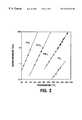
- FIG. 2is a graph of vapor pressure versus temperature for tantalum (Ta) halides.
- FIG. 3is a photograph of a scanning electron micrograph (SEM) of a tantalum nitride (TaN x ) film deposited using a tantalum pentafluoride (TaF 5 ) precursor.
- SEMscanning electron micrograph
- FIG. 4is a photograph of a SEM of a TaN x film deposited using a tantalum pentabromide (TaBr 5 ) precursor.
- FIG. 5is an Auger spectrum tracing of a TaN x film deposited using a TaBr 5 precursor deposited on a copper layer.
- Refractory transition metalssuch as tantalum (Ta) and their nitride films (TaN) are effective diffusion barriers to copper (Cu). Their effectiveness is due to their high thermal stability, high conductivity and resistance to diffusion of foreign elements or impurities. Ta and TaN are especially attractive due to their chemical inertness with Cu; no compounds form between Cu and Ta or Cu and N.
- Tantalum halidesprovide a convenient inorganic source for Ta and TaN.
- the inorganic precursoris a tantalum pentahalide (TaX 5 ) where X represents the halides fluorine (F), chlorine (Cl) and bromine (Br).
- Table 1shows relevant thermodynamic properties of the tantalum halide precursors, specifically tantalum pentafluoride (TaF 5 ), tantalum pentachloride (TaCl 5 ) and tantalum bromide (TaBr 5 ), with tantalum pentaiodide (Tal 5 ) included for comparison.
- the TaF 5 , TaCl 5 and TaBr 5 precursor materialsare all solids at room temperature (18° C.-22° C.).
- a chemical vapor deposition (CVD) system 10includes a CVD reaction chamber 11 and a precursor delivery system 12 .
- a reactionis carried out to convert a precursor gas of, for example, tantalum chloride (TaCl) or other tantalum halide compound, into a film such as a barrier layer film of tantalum (Ta) or tantalum nitride (TaN X ).
- the TaN filmis not limited to any particular stoichiometry (TaN x ), since TaN x can be continuously varied by changing the ratios of the gases in any given deposition.
- TaN xencompasses a tantalum nitride film of any stoichiometry.
- the precursor delivery system 12includes a source 13 of precursor gas having a gas outlet 14 , which communicates through a metering system 15 with a gas inlet 16 to the CVD reaction chamber 11 .
- the source 13generates a precursor vapor, for example a tantalum halide vapor, from a tantalum halide compound.
- the compoundis one that is in a solid state when at standard temperature and pressure.
- the precursor sourceis maintained, preferably by controlled heating, at a temperature that will produce a desired vapor pressure of precursor.
- the vapor pressureis one that is itself sufficient to deliver the precursor vapor to the reaction chamber 11 , preferably without the use of a carrier gas.
- the metering system 15maintains a flow of the precursor gas vapor from the source 13 into the reactor 11 at a rate that is sufficient to maintain a commercially viable CVD process in the reaction chamber 11 .
- the reaction chamber 11is a generally conventional CVD reactor and includes a vacuum chamber 20 that is bounded by a vacuum tight chamber wall 21 .
- a substrate support or susceptor 22on which a substrate such as a semiconductor wafer 23 is supported.
- the chamber 20is maintained at a vacuum appropriate for the performance of a CVD reaction that will deposit a film such as a Ta/TaN x barrier layer on the semiconductor wafer substrate 23 .
- a preferred pressure range for the CVD reaction chamber 11is in the range of from 0.2 to 5.0 Torr.
- the vacuumis maintained by controlled operation of a vacuum pump 24 and of inlet gas sources 25 that include the delivery system 12 and may also include reducing gas sources 26 of, for example, hydrogen (H 2 ), nitrogen (N 2 ) or ammonia (NH 3 ) for use in carrying out a tantalum reduction reaction, and an inert gas source 27 for a gas such as argon (Ar) or helium (He).
- reducing gas sources 26of, for example, hydrogen (H 2 ), nitrogen (N 2 ) or ammonia (NH 3 ) for use in carrying out a tantalum reduction reaction
- an inert gas source 27for a gas such as argon (Ar) or helium (He).
- the gases from the sources 25enter the chamber 20 through a showerhead 28 that is situated at one end of the chamber 20 opposite the substrate 23 , generally parallel to and facing the substrate 23 .
- the precursor gas source 13includes a sealed evaporator 30 that includes a cylindrical evaporation vessel 31 having a vertically oriented axis 32 .
- the vessel 31is bounded by a cylindrical wall 33 formed of a high temperature tolerant and non-corrosive material such as the alloy INCONEL 600, the inside surface 34 of which is highly polished and smooth.
- the wall 33has a flat circular closed bottom 35 and an open top, which is sealed by a cover 36 of the same heat tolerant and non-corrosive material as the wall 33 .
- the outlet 14 of the source 13is situated in the cover 36 .
- the cover 36is sealed to a flange ring 37 that is integral to the top of the wall 33 by a high temperature tolerant vacuum compatible metal seal 38 such as a HELICOFLEX seal, which is formed of a C-shaped nickel tube surrounding an INCONEL coil spring.
- a conventional elastomeric O-ring seal 38may be used to seal the cover.
- a source 39 of a carrier gaswhich is preferably an inert gas such as He or Ar.
- the source 13includes a mass of precursor material such as tantalum fluoride, chloride or bromide (TaX), preferably as the pentahalide (TaX 5 ), at the bottom of the vessel 31 , which is loaded into the vessel 31 at standard temperature and pressure in a solid state.
- the vessel 31is filled with tantalum halide vapor by sealing the chamber with the solid mass of TaX therein.
- the halideis supplied as a precursor mass 40 that is placed at the bottom of the vessel 31 , where it is heated, preferably to a liquid state as long as the resulting vapor pressure is in an acceptable range.
- Purge gas and TaX vaporsare, however, first evacuated from the vessel 31 with a vacuum pump 41 . Where the mass 40 is liquid, the vapor lies above the level of the liquid mass 40 . Because wall 33 is a vertical cylinder, the surface area of TaX mass 40 , if a liquid, remains constant regardless of the level of depletion of the TaX.
- the delivery system 12is not limited to direct delivery of a precursor 40 but can be used in the alternative for delivery of precursor 40 along with a carrier gas, which can be introduced into the vessel 31 from gas source 39 .
- a carrier gasmay be hydrogen (H 2 ) or an inert gas such as helium (He) or argon (Ar).
- a carrier gasmay be introduced into the vessel 31 so as to distribute across the top surface of the precursor mass 40 or may be introduced into the vessel 31 so as to percolate through the mass 40 from the bottom 35 of the vessel 31 with upward diffusion in order to achieve maximum surface area exposure of the mass 40 to the carrier gas.
- a carrier gasmay be introduced into the vessel 31 so as to distribute across the top surface of the precursor mass 40 or may be introduced into the vessel 31 so as to percolate through the mass 40 from the bottom 35 of the vessel 31 with upward diffusion in order to achieve maximum surface area exposure of the mass 40 to the carrier gas.
- Yet another alternativeis to vaporize a liquid that is in the vessel 31 .
- such alternativesadd
- the bottom 35 of the wall 33is maintained in thermal communication with a heater 44 , which maintains the precursor 40 at a controlled temperature, preferably above its melting point, that will produce a vapor pressure of greater than about 3 Torr in the absence of a carrier gas (i.e., a direct delivery system), and a lower vapor pressure such as about 1 Torr when a carrier gas is used.
- a carrier gasi.e., a direct delivery system
- a lower vapor pressuresuch as about 1 Torr when a carrier gas is used.
- the exact vapor pressuredepends upon other variables such as the quantity of carrier gas, the surface area of the substrate 23 , and so on.
- a vapor pressurecan be maintained at the preferred pressure of 5 Torr or above by heating the a tantalum halide precursor in the 95° C. to 205° C.
- the desired temperatureis at least about 95° C. for TaF 5
- the desired temperatureis at least about 145° C. for TaCl 5
- the desired temperatureis at least about 205° C. for TaBr 5 .
- the melting points of the respective fluoride, chloride and bromide tantalum pentahalide compoundsare in the 97° C. to 265° C. range.
- a much higher temperatureis required for tantalum pentaiodide (Tal 5 ) to produce a sufficient vapor pressure in the vessel 31 .
- Temperaturesshould not be so high as to cause premature reaction of the gases in the showerhead 28 or otherwise before contacting the wafer 23 .
- a temperature of 180° C.is assumed to be the control temperature for the heating of the bottom 35 of the vessel 31 .
- This temperatureis appropriate for producing a desired vapor pressure with a titanium tetraiodide (Til 4 ) precursor.
- Ti 4titanium tetraiodide
- the coveris maintained at a higher temperature than the heater 44 at the bottom 35 of the wall 33 of, for example, 190° C., by a separately controlled heater 45 that is in thermal contact with the outside of the cover 36 .
- the sides of the chamber wall 33are surrounded by an annular trapped air space 46 , which is contained between the chamber wall 33 and a surrounding concentric outer aluminum wall or can 47 .
- the can 47is further surrounded by an annular layer of silicon foam insulation 48 .
- This temperature maintaining arrangementmaintains the vapor in a volume of the vessel 31 bounded by the cover 36 , the sides of the walls 33 and the surface 42 of the precursor mass 40 in the desired example temperature range of between 180° C. and 190° C. and the pressure greater than about 3 Torr, preferably at greater than 5 Torr.
- the temperature that is appropriate to maintain the desired pressurewill vary with the precursor material, which is primarily contemplated as a being a tantalum or titanium halide compound.
- the vapor flow metering system 15includes a delivery tube 50 of at least 1 ⁇ 2 inch in diameter, or at least 10 millimeters inside diameter, and preferably larger so as to provide no appreciable pressure drop at the flow rate desired, which is at least approximately 2 to 40 standard cubic centimeters per minute (sccm).
- the tube 50extends from the precursor gas source 13 to which it connects at its upstream end to the outlet 14 , to the reactor 11 to which it connects at its downstream end to the inlet 16 .
- the entire length of the tube 50 from the evaporator outlet 14 to the reactor inlet 16 and the showerhead 28 of the reactor chamber 20are also preferably heated to above the evaporation temperature of the precursor material 40 , for example, to 195° C.
- baffle plate 51in which is centered a circular orifice 52 , which preferably has a diameter of approximately 0.089 inches.
- the pressure drop from gauge 156 to gauge 2 57is regulated by control valve 53 .
- This pressure drop after control valve 53 through orifice 52 and into reaction chamber 11is greater than about 10 milliTorr and will be proportional to the flow rate.
- a shut-off valve 54is provided in the line 50 between the outlet 14 of the evaporator 13 and the control valve 53 to close the vessel 31 of the evaporator 13 .
- Pressure sensors 55 - 58are provided in the system 10 to provide information to a controller 60 for use in controlling the system 10 , including controlling the flow rate of precursor gas from the delivery system 15 into the chamber 20 of the CVD reactor 11 .
- the pressure sensorsinclude sensor 55 connected to the tube 50 between the outlet 14 of the evaporator 13 and the shut-off valve 54 to monitor the pressure in the evaporation vessel 31 .
- a pressure sensor 56is connected to the tube 50 between the control valve 53 and the baffle 51 to monitor the pressure upstream of the orifice 52
- a pressure sensor 57is connected to the tube 50 between the baffle 51 and the reactor inlet 16 to monitor the pressure downstream of the orifice 52 .
- a further pressure sensor 58is connected to the chamber 20 of the reaction chamber 11 to monitor the pressure in the CVD chamber 20 .
- Control of the flow of precursor vapor into the CVD chamber 20 of the reaction chamber 11is achieved by the controller 60 in response to the pressures sensed by the sensors 55 - 58 , particularly the sensors 56 and 57 which determine the pressure drop across the orifice 52 .
- the actual flow of precursor vapor through the tube 52is a function of the pressures monitored by pressure sensors 56 and 57 , and can be determined from the ratio of the pressure measured by sensor 56 on the upstream side of the orifice 52 , to the pressure measured by sensor 57 on the downstream side of the orifice 52 .
- the actual flow of precursor vapor through the tube 52is a function of only the pressure monitored by pressure sensor 57 .
- the existence of choked or unchoked flowcan be determined by the controller 60 by interpreting the process conditions.
- the flow rate of precursor gascan be determined by the controller 60 through calculation.
- accurate determination of the actual flow rate of precursor gasis calculated by retrieving flow rate data from lookup or multiplier tables stored in a non-volatile memory 61 accessible by the controller 60 .
- the desired flow ratecan be maintained by a closed loop feedback control of one or more of the variable orifice control valve 53 , the CVD chamber pressure through evacuation pump 24 or control of reducing or inert gases from sources 26 and 27 , or by control of the temperature and vapor pressure of the precursor gas in vessel 31 by control of heaters 44 , 45 .
- the solid TaF 5 , TaCl 5 and TaBr 5 precursor material 40is sealed in a cylindrical corrosion resistant metal vessel 31 that maximizes the available surface area of the precursor material.
- Vapor from either TaF 5 , TaCl 5 or TaBr 5was delivered directly, that is, without the use of a carrier gas, by a high conductance delivery system into a reaction chamber 11 .
- the reaction chamber 11was heated to a temperature of at least about 100° C. to prevent condensation of vapor or deposition by-products.
- the controlled direct delivery of tantalum halide vapor into the reaction chamber 11was accomplished by heating the solid tantalum halide precursor 40 to a temperature in the range of about 95° C.-205° C., the choice depending upon the particular precursor. The temperature was sufficient to vaporize the precursor 40 to provide a vapor pressure to deliver the tantalum halide vapor to the chamber 11 . Thus, a carrier gas was not necessary. A sufficient vapor pressure was greater than about 3 Torr. This pressure was required to maintain a constant pressure drop across a defined orifice in a high conductance delivery system while delivering up to about 50 sccm tantalum halide precursor to a reaction chamber 11 operating in the range of about 0.1-2.0 Torr.
- the temperatures to obtain the desired pressures in a direct delivery systemwere in the range of about 83° C.-95° C. and preferably about 95° C. with TaF 5 , in the range of about 130° C.-150° C. and preferably about 145° C. with TaCl 5 , and in the range of about 202° C.-218° C. and preferably about 205° C. with TaBr 5 . Under these conditions, TaF 5 is a liquid while TaCl 5 and TaBr 5 remain solid.
- FIG. 2shows the relationship between the measured vapor pressure and temperature for the precursors TaF 5 , TaCl 5 and TaBr 5 , with Tal 5 included for comparison.
- the desired pressurewas greater than about 3 Torr and preferably greater than 5 Torr.
- the vapor pressure for TaF 5 , TaCl 5 and TaBr 5was desirably low enough to be able to deposit tantalum in the absence of a carrier gas but yet sufficient to maintain a constant pressure drop across a defined orifice in a high conductance delivery system and still be able to deliver up to 50 sscm TaX 5 to a reaction chamber 11 operating at 0.1-2.0 Torr.
- the vapor pressure for Tal 5was determined to be too low for practical implementation in the described apparatus.
- the open circlesrepresent published values, while closed squares for TaBr 5 , TaF 5 , TaCl 5 and Tal 5 represent the inventors' experimental data.
- the selected TaX 5 vaporwas combined with ammonia (NH 3 ) above the substrate, which had been heated to a temperature between about 300° C.-500° C.
- Argon (Ar)nitrogen (N 2 ), hydrogen (H 2 ) and helium (He) could also be used, either singularly or in combination, as process gases.
- Process conditions for deposition of good quality thermal CVD tantalum nitride filmsare given in Table 2, where slm is standard liters per minute and W/cm 2 is watts per centimeter squared.
- TaX 5 temperature95° C. (TaF 5 ), 145° C. (TaCl 5 ), 205° C. (TaBr 5 )
- TaX 5 flow1-50 sccm H 2 flow 0-10 slm Ar, He flow 0-10 slm Process Pressure 0.2-5.0 Torr NH 3 flow 0.1-10 slm N 2 flow 0-10 slm
- the film deposited by the method of the inventiondisplays characteristics important to the formation of an IC.
- the filmis in the range of low enough electrical resistivity for low interconnect impedences (less than 1000 ⁇ cm and preferably less than 500 ⁇ cm), and the film has good conformality and good step coverage (greater than 0.3).
- the level of impuritiesare low (less than 2 atomic percent).
- the deposition ratesare sufficient for throughput considerations (greater than 100 ⁇ /min) and the process uses a low wafer temperature (less than 450° C.) and thus is compatible with other thin film materials used in the device, including materials with dielectric constants lower than that of SiO 2 .
- a TaN x film deposited using a TaF 5 precursor at a flow of 6 sccmhad a resistivity of greater than about 1 ⁇ 10 7 ⁇ cm. Under these conditions the deposition rate was 850 ⁇ /min and the step coverage was 0.2. As the TaF 5 precursor flow was increased to 10 sccm with the temperature maintained at 415° C., the pressure maintained at 0.3 Torr and the NH 3 flow maintained at 1.0 slm, the resistivity decreased to 7 ⁇ 10 6 ⁇ cm.
- the deposition rateincreased to 1000 ⁇ /min and the step coverage increased to 1.0.
- the TaF 5 precursor flowwas further increased to 28 sccm with the temperature maintained at 415° C., the pressure maintained at 0.3 Torr and the NH 3 flow maintained at 1.0 slm, the resistivity further decreased to 4 ⁇ 10 5 ⁇ cm.
- the deposition rateincreased to 1115 ⁇ /min while the step coverage remained at 1.0.
- a TaN film deposited using a TaBr 5 precursor at a flow of 10 sccmhad a resistivity of greater than about 1 ⁇ 10 7 ⁇ cm. Under these conditions the deposition rate was 200 ⁇ /min and the step coverage was 0.6.
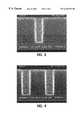
- FIGS. 3-4Scanning electron micrographs (SEM) of TaN x films deposited by thermal CVD according to the invention were obtained and are shown in FIGS. 3-4.
- FIG. 3is a SEM of a TaN x film using TaF 5 as the precursor.
- FIG. 4is a SEM of a TaN x film using TaBr 5 as the precursor.
- FIG. 3 and FIG. 4shows a 3:1 aspect ratio structure with representative bottom step coverage and side wall coverage for TaF 5 and TaBr 5 precursors.
- the step coveragerepresents the film thickness on the bottom of the feature divided by the film thickness on the surface of the substrate adjacent the feature, also called the field.
- Table 3the step coverage for TaF 5 precursor TaN x films with a TaF 5 flow of 6 sccm was 0.2.
- the step coverageincreased to 1.0 when the TaF 5 flow was increased to either 10 sccm or 28 sccm while the temperature was maintained at 415° C.
- the step coverage for TaBr 5 precursor TaN filmswas 0.6 at a TaBr 5 flow of 10 sccm and a temperature of 425° C.
- the TaF 5 based TaN x filmappeared to have better step coverage than the TaBr 5 based TaN film.
- the TaN x filmsgenerally appeared to have good dense morphologies.
- the TaBr 5 based TaN x filmgenerally appeared to be smoother than the TaF 5 based film, which appeared rougher. Based on experience with other films using TaF 5 and TaBr 5 precursors, it is presumed that TaCl 5 based TaN x films deposited according to the method of the invention would yield an intermediate step coverage and film morphology between TaF 5 and TaBr 5 based TaN x films.
- Ta compatibility with copperwas determined. Since in practice the Ta film will be integral, that is, in direct contact with copper, little or no attack or etching of the copper should take place during Ta deposition. Ta compatibility with copper was tested by placing a Si wafer containing a 500 ⁇ layer of titanium nitride (TiN) deposited by PVD and a 2000 ⁇ layer of copper deposited by PVD into the reaction chamber 11 . A Ta film was deposited by PECVD on top of the copper layer using the process of the invention with either a TaF 5 , TaCl 5 or TaBr 5 precursor.
- TiNtitanium nitride
- the resulting filmwas evaluated by Auger electron spectroscopy. Analysis of the Auger spectrum confirmed the clean interface and the minimal diffusion between the Cu and TaN x layer. The analysis also determined the level of impurities present in the film.
- the Auger analysis spectrumis shown in FIG. 5 with TaBr 5 used as the precursor for depositing TaN x on a Cu layer in a Cu/TiN/Si stack.
- FIG. 5indicates that the TaN x film was nitrogen rich (x>1.0), which is consistent with the results shown in Table 3.
- the N 2 rich TaN x filmis expected to have a relatively high electrical resistivity.
- FIG. 5also shows a good sharp interface between the TaN x layer and Cu, which suggests little or no attack of the Cu surface during TaN deposition.
- the bromide concentrationwas determined to be less than 2 atomic percent.
- TaF 5 based TaN x films deposited by thermal CVD according to the method of the inventionappearmost promising due to the high deposition rate and 100% step coverage.
- Ta filmsmay be deposited by PECVD
- TaN x filmsmay be deposited by PECVD or plasma treated thermal CVD as disclosed in, respectively, PECVD OF Ta FILMS FROM TANTALUM HALIDE PRECURSORS (Ser. No. 09/300,583), PECVD OF TaN FILMS FROM TANTALUM HALIDE PRECURSORS (U.S. Pat. No. 6,265,311) and PLASMA TREATED THERMAL CVD OF TaN FILMS FROM TANTALUM HALIDE PRECURSORS (U.S. Pat. No.
- Ta/TaN x bilayersmay be deposited by CVD and TaN x , may be used for plug fill according to the invention as disclosed in, respectively, INTEGRATION OF CVD Ta AND TaN, FILMS FROM TANTALUM HALIDE PRECURSORS (Ser. No. 09/300,632) and CVD TaN x PLUG FORMATION FROM TANTALUM HALIDE PRECURSORS (Ser. No.
Landscapes
- Chemical & Material Sciences (AREA)
- Engineering & Computer Science (AREA)
- Computer Hardware Design (AREA)
- Microelectronics & Electronic Packaging (AREA)
- General Chemical & Material Sciences (AREA)
- Condensed Matter Physics & Semiconductors (AREA)
- General Physics & Mathematics (AREA)
- Manufacturing & Machinery (AREA)
- Chemical Kinetics & Catalysis (AREA)
- Physics & Mathematics (AREA)
- Power Engineering (AREA)
- Inorganic Chemistry (AREA)
- Materials Engineering (AREA)
- Mechanical Engineering (AREA)
- Metallurgy (AREA)
- Organic Chemistry (AREA)
- Chemical Vapour Deposition (AREA)
- Electrodes Of Semiconductors (AREA)
Abstract
Description
The invention relates to the formation of integrated circuits, and specifically to chemical vapor deposition of tantalum nitride films from tantalum halide precursors.
Integrated circuits (IC) provide the pathways for signal transport in an electrical device. An IC in a device is composed of a number of active transistors contained in a silicon base layer of a semiconductor substrate. To increase the capacity of an IC, large numbers of interconnections with metal “wires” are made between one active transistor in the silicon base of the substrate and another active transistor in the silicon base of the substrate. The interconnections, collectively known as the metal interconnection of a circuit, are made through holes, vias or trenches that are cut into a substrate. The particular point of the metal interconnection which actually makes contact with the silicon base is known as the contact. The remainder of the hole, via or trench is filled with a conductive material, termed a contact plug. As transistor densities continue to increase, forming higher level integrated circuits, the diameter of the contact plug must decrease to allow for the increased number of interconnections, multilevel metalization structures and higher aspect ratio vias.
Aluminum has been the accepted standard for contacts and interconnections in integrated circuits. However, problems with its electromigration and its high electrical resistivity require new materials for newer structures with submicron dimensions. Copper holds promise as the interconnect material for the next generation of integrated circuits in ultra large scale integration (ULSI) circuitry, yet its formation of copper silicide (Cu—Si) compounds at low temperatures and its electromigration through a silicon oxide (SiO2) are disadvantages to its use.
As the shift from aluminum to copper as an interconnect element of choice occurs, new materials are required to serve as a barrier, preventing copper diffusion into the underlying dielectric layers of the substrate and to form an effective “glue” layer for subsequent copper deposition. New materials are also required to serve as a liner, adhering subsequently deposited copper to the substrate. The liner must also provide a low electrical resistance interface between copper and the barrier material. Barrier layers that were previously used with aluminum, such as titanium (Ti) and titanium nitride (TiN) barrier layers deposited either by physical vapor deposition (PVD) methods such as sputtering and/or chemical vapor deposition (CVD), are ineffective as barriers to copper. In addition, Ti reacts with copper to form copper titanium compounds at the relatively low temperatures used with PVD and/or CVD.
Sputtered tantalum (Ta) and reactive sputtered tantalum nitride (TaN) have been demonstrated to be good diffusion barriers between copper and a silicon substrate due to their high conductivity, high thermal stability and resistance to diffusion of foreign atoms. However, the deposited Ta and/or TaN film has inherently poor step coverage due to its shadowing effects. Thus the sputtering process is limited to relatively large feature sizes (>0.3 μm) and small aspect ratio contact vias. CVD offers the inherent advantage over PVD of better conformality, even in small structures (<0.25 μm) with high aspect ratios. However, CVD of Ta and TaN with metal-organic sources such as tertbutylimidotris(diethylamido)tantalum (TBTDET), pentakis(dimethylamino)tantalum (PDMAT) and pentakis(diethylamino)tantalum (PDEAT) yields mixed results. Additional problems with Ta and TaN are that all resulting films have relatively high concentrations of oxygen and carbon impurities and require the use of a carrier gas.
The need to use a carrier gas presents the disadvantage that the concentration of the precursor gas in the carrier is not precisely known. As a result, accurate metering of a mixture of a carrier gas and a precursor gas to the CVD reaction chamber does not insure accurate metering of the precursor gas alone to the reactor. This can cause the reactants in the CVD chamber to be either too rich or too lean. The use of a carrier gas also presents the disadvantage that particulates are frequently picked up by the flowing carrier gas and delivered as contaminants to the CVD reaction chamber. Particulates on the surface of a semiconductor wafer during processing can result in the production of defective semiconductor devices.
Thus, a process to deposit TaN by a thermal CVD method would provide an advantage in the formation of copper barriers in the next generation of IC. Ideally, the deposited film will have a high step coverage (the ratio of the coating thickness at the bottom of a feature to the thickness on the sides of a feature or on the top surface of the substrate or wafer adjacent the feature), good diffusion barrier properties, minimal impurities, low resistivity, good conformality (even coverage of complex topography of high aspect ratio features) and ideally the process will have a high deposition rate.
The invention is directed to a method of depositing a tantalum nitride (TaNx) film from a tantalum halide precursor on a substrate. The tantalum halide precursor is delivered at a temperature sufficient to vaporize the precursor to provide a vaporization pressure to deliver the tantalum vapor to a reaction chamber containing the substrate. The vaporization pressure is greater than about 3 Torr. The vapor is combined with a process gas containing nitrogen and TaNxis deposited on the substrate by a thermal chemical vapor deposition (CVD) process. The tantalum halide precursor is tantalum fluoride (TaF), tantalum chloride (TaCl) or tantalum bromide (TaBr), preferably tantalum pentafluoride (TaF5), tantalum pentachloride (TaCl5) or tantalum pentabromide (TaBr5). The substrate temperature is in the range of about 300° C.-500° C.
The invention is also directed to a method of depositing a TaNxfilm from a TaF5or TaCl5precursor on a substrate by elevating the precursor temperature sufficient to vaporize the precursor. The vapor is combined with a process gas containing nitrogen and the TaNxfilm is deposited by thermal CVD.
The invention is further directed to method of depositing a TaNxfilm from a TaBr5precursor on a substrate without a carrier gas. The temperature of the precursor is elevated sufficient to produce a tantalum vapor. The vapor is combined with a process gas containing nitrogen and the TaNxfilm is deposited on the substrate by thermal CVD.
The invention is still further directed to a substrate integral with a copper layer and a TaNxlayer in which diffusion of copper is prevented by the TaNxlayer.
The TaNxlayer deposited according to the invention has minimal impurities and low resistivity. The film provides good step coverage, good conformality in high aspect ratio features and is a good diffusion barrier to a copper film.
It will be appreciated that the disclosed method and substrates of the invention have an array of applications. These and other advantages will be further understood with reference to the following drawings and detailed description.
FIG. 1 is a schematic of an apparatus for thermal chemical vapor deposition (CVD).
FIG. 2 is a graph of vapor pressure versus temperature for tantalum (Ta) halides.
FIG. 3 is a photograph of a scanning electron micrograph (SEM) of a tantalum nitride (TaNx) film deposited using a tantalum pentafluoride (TaF5) precursor.
FIG. 4 is a photograph of a SEM of a TaNxfilm deposited using a tantalum pentabromide (TaBr5) precursor.
FIG. 5 is an Auger spectrum tracing of a TaNxfilm deposited using a TaBr5precursor deposited on a copper layer.
Refractory transition metals such as tantalum (Ta) and their nitride films (TaN) are effective diffusion barriers to copper (Cu). Their effectiveness is due to their high thermal stability, high conductivity and resistance to diffusion of foreign elements or impurities. Ta and TaN are especially attractive due to their chemical inertness with Cu; no compounds form between Cu and Ta or Cu and N.
Tantalum halides provide a convenient inorganic source for Ta and TaN. Specifically, the inorganic precursor is a tantalum pentahalide (TaX5) where X represents the halides fluorine (F), chlorine (Cl) and bromine (Br). Table 1 shows relevant thermodynamic properties of the tantalum halide precursors, specifically tantalum pentafluoride (TaF5), tantalum pentachloride (TaCl5) and tantalum bromide (TaBr5), with tantalum pentaiodide (Tal5) included for comparison. The TaF5, TaCl5and TaBr5precursor materials are all solids at room temperature (18° C.-22° C.).
| TABLE 1 | |||
| MELTING | BOILING | CHANGE IN HEAT OF | |
| PRECURSOR | POINT | POINT | FORMATION (ΔHf) |
| TaF5 | 97° C. | 230° C. | −455 kcal/mole |
| TaCl5 | 216° C. | 242° C. | −205 kcal/mole |
| TaBr5 | 265° C. | 349° C. | −143 kcal/mole |
| Tal5 | 367° C. | 397° C. | −82 kcal/mole |
In chemical vapor deposition (CVD) processes, gas precursors are activated using either thermal energy or electrical energy. Upon activation, the gas precursors react chemically to form a film. A preferred method of CVD is illustrated in FIG.1 and is disclosed in copending application Ser. No. 09/300,669, now abandoned, entitled APPARATUS AND METHODS FOR DELIVERY OF VAPOR FROM SOLID SOURCES TO A CVD CHAMBER by Westendorp et al. filed on the same date as the present application and assigned to Tokyo Electron Limited and incorporated by reference herein in its entirety. A chemical vapor deposition (CVD)system 10 includes a CVD reaction chamber11 and a precursor delivery system12. In the reaction chamber11, a reaction is carried out to convert a precursor gas of, for example, tantalum chloride (TaCl) or other tantalum halide compound, into a film such as a barrier layer film of tantalum (Ta) or tantalum nitride (TaNX). The TaN film is not limited to any particular stoichiometry (TaNx), since TaNxcan be continuously varied by changing the ratios of the gases in any given deposition. Thus, as used herein, TaNxencompasses a tantalum nitride film of any stoichiometry.
The precursor delivery system12 includes asource 13 of precursor gas having a gas outlet14, which communicates through ametering system 15 with a gas inlet16 to the CVD reaction chamber11. Thesource 13 generates a precursor vapor, for example a tantalum halide vapor, from a tantalum halide compound. The compound is one that is in a solid state when at standard temperature and pressure. The precursor source is maintained, preferably by controlled heating, at a temperature that will produce a desired vapor pressure of precursor. Preferably, the vapor pressure is one that is itself sufficient to deliver the precursor vapor to the reaction chamber11, preferably without the use of a carrier gas. Themetering system 15 maintains a flow of the precursor gas vapor from thesource 13 into the reactor11 at a rate that is sufficient to maintain a commercially viable CVD process in the reaction chamber11.
The reaction chamber11 is a generally conventional CVD reactor and includes avacuum chamber 20 that is bounded by a vacuumtight chamber wall 21. In thechamber 20 is situated a substrate support orsusceptor 22 on which a substrate such as a semiconductor wafer23 is supported. Thechamber 20 is maintained at a vacuum appropriate for the performance of a CVD reaction that will deposit a film such as a Ta/TaNxbarrier layer on the semiconductor wafer substrate23. A preferred pressure range for the CVD reaction chamber11 is in the range of from 0.2 to 5.0 Torr. The vacuum is maintained by controlled operation of avacuum pump 24 and of inlet gas sources25 that include the delivery system12 and may also include reducinggas sources 26 of, for example, hydrogen (H2), nitrogen (N2) or ammonia (NH3) for use in carrying out a tantalum reduction reaction, and an inert gas source27 for a gas such as argon (Ar) or helium (He). The gases from the sources25 enter thechamber 20 through ashowerhead 28 that is situated at one end of thechamber 20 opposite the substrate23, generally parallel to and facing the substrate23.
Theprecursor gas source 13 includes a sealedevaporator 30 that includes a cylindrical evaporation vessel31 having a vertically orientedaxis 32. The vessel31 is bounded by acylindrical wall 33 formed of a high temperature tolerant and non-corrosive material such as the alloy INCONEL 600, theinside surface 34 of which is highly polished and smooth. Thewall 33 has a flat circular closed bottom35 and an open top, which is sealed by a cover36 of the same heat tolerant and non-corrosive material as thewall 33. The outlet14 of thesource 13 is situated in the cover36. When high temperatures are used, such as with Til4or TaBr5, the cover36 is sealed to a flange ring37 that is integral to the top of thewall 33 by a high temperature tolerant vacuum compatible metal seal38 such as a HELICOFLEX seal, which is formed of a C-shaped nickel tube surrounding an INCONEL coil spring. With TaCl5and TaF5, a conventional elastomeric O-ring seal38 may be used to seal the cover.
Connected to the vessel31 through the cover36 is asource 39 of a carrier gas, which is preferably an inert gas such as He or Ar. Thesource 13 includes a mass of precursor material such as tantalum fluoride, chloride or bromide (TaX), preferably as the pentahalide (TaX5), at the bottom of the vessel31, which is loaded into the vessel31 at standard temperature and pressure in a solid state. The vessel31 is filled with tantalum halide vapor by sealing the chamber with the solid mass of TaX therein. The halide is supplied as aprecursor mass 40 that is placed at the bottom of the vessel31, where it is heated, preferably to a liquid state as long as the resulting vapor pressure is in an acceptable range. Purge gas and TaX vapors are, however, first evacuated from the vessel31 with avacuum pump 41. Where themass 40 is liquid, the vapor lies above the level of theliquid mass 40. Becausewall 33 is a vertical cylinder, the surface area ofTaX mass 40, if a liquid, remains constant regardless of the level of depletion of the TaX.
The delivery system12 is not limited to direct delivery of aprecursor 40 but can be used in the alternative for delivery ofprecursor 40 along with a carrier gas, which can be introduced into the vessel31 fromgas source 39. Such a gas may be hydrogen (H2) or an inert gas such as helium (He) or argon (Ar). Where a carrier gas is used, it may be introduced into the vessel31 so as to distribute across the top surface of theprecursor mass 40 or may be introduced into the vessel31 so as to percolate through the mass40 from the bottom35 of the vessel31 with upward diffusion in order to achieve maximum surface area exposure of the mass40 to the carrier gas. Yet another alternative is to vaporize a liquid that is in the vessel31. However, such alternatives add undesired particulates and do not provide the controlled delivery rate achieved by the direct delivery of the precursor, that is, delivery without the use of a carrier gas. Therefore, direct delivery of the precursor is preferred.
To maintain the temperature of theprecursor 40 in the vessel31, the bottom35 of thewall 33 is maintained in thermal communication with aheater 44, which maintains theprecursor 40 at a controlled temperature, preferably above its melting point, that will produce a vapor pressure of greater than about 3 Torr in the absence of a carrier gas (i.e., a direct delivery system), and a lower vapor pressure such as about 1 Torr when a carrier gas is used. The exact vapor pressure depends upon other variables such as the quantity of carrier gas, the surface area of the substrate23, and so on. In a direct delivery system for tantalum, a vapor pressure can be maintained at the preferred pressure of 5 Torr or above by heating the a tantalum halide precursor in the 95° C. to 205° C. range as shown in FIG.2. For TaX5the desired temperature is at least about 95° C. for TaF5, the desired temperature is at least about 145° C. for TaCl5, and the desired temperature is at least about 205° C. for TaBr5. The melting points of the respective fluoride, chloride and bromide tantalum pentahalide compounds are in the 97° C. to 265° C. range. A much higher temperature is required for tantalum pentaiodide (Tal5) to produce a sufficient vapor pressure in the vessel31. Temperatures should not be so high as to cause premature reaction of the gases in theshowerhead 28 or otherwise before contacting the wafer23.
For purposes of example, a temperature of 180° C. is assumed to be the control temperature for the heating of the bottom35 of the vessel31. This temperature is appropriate for producing a desired vapor pressure with a titanium tetraiodide (Til4) precursor. Given this temperature at the bottom35 of the vessel31, to prevent condensation of the precursor vapor on thewalls 33 and cover36 of the vessel31, the cover is maintained at a higher temperature than theheater 44 at the bottom35 of thewall 33 of, for example, 190° C., by a separately controlledheater 45 that is in thermal contact with the outside of the cover36. The sides of thechamber wall 33 are surrounded by an annulartrapped air space 46, which is contained between thechamber wall 33 and a surrounding concentric outer aluminum wall or can47. Thecan 47 is further surrounded by an annular layer ofsilicon foam insulation 48. This temperature maintaining arrangement maintains the vapor in a volume of the vessel31 bounded by the cover36, the sides of thewalls 33 and thesurface 42 of theprecursor mass 40 in the desired example temperature range of between 180° C. and 190° C. and the pressure greater than about 3 Torr, preferably at greater than 5 Torr. The temperature that is appropriate to maintain the desired pressure will vary with the precursor material, which is primarily contemplated as a being a tantalum or titanium halide compound.
The vaporflow metering system 15 includes adelivery tube 50 of at least ½ inch in diameter, or at least 10 millimeters inside diameter, and preferably larger so as to provide no appreciable pressure drop at the flow rate desired, which is at least approximately 2 to 40 standard cubic centimeters per minute (sccm). Thetube 50 extends from theprecursor gas source 13 to which it connects at its upstream end to the outlet14, to the reactor11 to which it connects at its downstream end to the inlet16. The entire length of thetube 50 from the evaporator outlet14 to the reactor inlet16 and theshowerhead 28 of thereactor chamber 20 are also preferably heated to above the evaporation temperature of theprecursor material 40, for example, to 195° C.
In thetube 50 is provided baffle plate51 in which is centered a circular orifice52, which preferably has a diameter of approximately 0.089 inches. The pressure drop from gauge156 to gauge257 is regulated bycontrol valve 53. This pressure drop aftercontrol valve 53 through orifice52 and into reaction chamber11 is greater than about 10 milliTorr and will be proportional to the flow rate. A shut-off valve54 is provided in theline 50 between the outlet14 of theevaporator 13 and thecontrol valve 53 to close the vessel31 of theevaporator 13.
Pressure sensors55-58 are provided in thesystem 10 to provide information to acontroller 60 for use in controlling thesystem 10, including controlling the flow rate of precursor gas from thedelivery system 15 into thechamber 20 of the CVD reactor11. The pressure sensors includesensor 55 connected to thetube 50 between the outlet14 of theevaporator 13 and the shut-off valve54 to monitor the pressure in the evaporation vessel31. Apressure sensor 56 is connected to thetube 50 between thecontrol valve 53 and the baffle51 to monitor the pressure upstream of the orifice52, while apressure sensor 57 is connected to thetube 50 between the baffle51 and the reactor inlet16 to monitor the pressure downstream of the orifice52. Afurther pressure sensor 58 is connected to thechamber 20 of the reaction chamber11 to monitor the pressure in theCVD chamber 20.
Control of the flow of precursor vapor into theCVD chamber 20 of the reaction chamber11 is achieved by thecontroller 60 in response to the pressures sensed by the sensors55-58, particularly thesensors pressure sensors sensor 56 on the upstream side of the orifice52, to the pressure measured bysensor 57 on the downstream side of the orifice52.
When the conditions are such that the flow of precursor vapor through the orifice52 is choked flow, the actual flow of precursor vapor through the tube52 is a function of only the pressure monitored bypressure sensor 57. In either case, the existence of choked or unchoked flow can be determined by thecontroller 60 by interpreting the process conditions. When the determination is made by thecontroller 60, the flow rate of precursor gas can be determined by thecontroller 60 through calculation.
Preferably, accurate determination of the actual flow rate of precursor gas is calculated by retrieving flow rate data from lookup or multiplier tables stored in anon-volatile memory 61 accessible by thecontroller 60. When the actual flow rate of the precursor vapor is determined, the desired flow rate can be maintained by a closed loop feedback control of one or more of the variableorifice control valve 53, the CVD chamber pressure throughevacuation pump 24 or control of reducing or inert gases fromsources 26 and27, or by control of the temperature and vapor pressure of the precursor gas in vessel31 by control ofheaters
As shown in FIG. 1, the solid TaF5, TaCl5and TaBr5precursor material40 is sealed in a cylindrical corrosion resistant metal vessel31 that maximizes the available surface area of the precursor material. Vapor from either TaF5, TaCl5or TaBr5was delivered directly, that is, without the use of a carrier gas, by a high conductance delivery system into a reaction chamber11. The reaction chamber11 was heated to a temperature of at least about 100° C. to prevent condensation of vapor or deposition by-products.
The controlled direct delivery of tantalum halide vapor into the reaction chamber11 was accomplished by heating the solidtantalum halide precursor 40 to a temperature in the range of about 95° C.-205° C., the choice depending upon the particular precursor. The temperature was sufficient to vaporize theprecursor 40 to provide a vapor pressure to deliver the tantalum halide vapor to the chamber11. Thus, a carrier gas was not necessary. A sufficient vapor pressure was greater than about 3 Torr. This pressure was required to maintain a constant pressure drop across a defined orifice in a high conductance delivery system while delivering up to about 50 sccm tantalum halide precursor to a reaction chamber11 operating in the range of about 0.1-2.0 Torr. The temperatures to obtain the desired pressures in a direct delivery system were in the range of about 83° C.-95° C. and preferably about 95° C. with TaF5, in the range of about 130° C.-150° C. and preferably about 145° C. with TaCl5, and in the range of about 202° C.-218° C. and preferably about 205° C. with TaBr5. Under these conditions, TaF5is a liquid while TaCl5and TaBr5remain solid.
FIG. 2 shows the relationship between the measured vapor pressure and temperature for the precursors TaF5, TaCl5and TaBr5, with Tal5included for comparison. As previously stated, the desired pressure was greater than about 3 Torr and preferably greater than 5 Torr. Also as previously stated, the vapor pressure for TaF5, TaCl5and TaBr5was desirably low enough to be able to deposit tantalum in the absence of a carrier gas but yet sufficient to maintain a constant pressure drop across a defined orifice in a high conductance delivery system and still be able to deliver up to 50 sscm TaX5to a reaction chamber11 operating at 0.1-2.0 Torr. The vapor pressure for Tal5was determined to be too low for practical implementation in the described apparatus. For TaBr5the open circles represent published values, while closed squares for TaBr5, TaF5, TaCl5and Tal5represent the inventors' experimental data.
The selected TaX5vapor was combined with ammonia (NH3) above the substrate, which had been heated to a temperature between about 300° C.-500° C. Argon (Ar), nitrogen (N2), hydrogen (H2) and helium (He) could also be used, either singularly or in combination, as process gases. Process conditions for deposition of good quality thermal CVD tantalum nitride films are given in Table 2, where slm is standard liters per minute and W/cm2is watts per centimeter squared.
| TABLE 2 | |
| Substrate Temperature | 300° C.-500° C. |
| TaX5temperature | 95° C. (TaF5), 145° C. (TaCl5), 205° C. (TaBr5) |
| TaX5flow | 1-50 sccm |
| H2flow | 0-10 slm |
| Ar, He flow | 0-10 slm |
| Process Pressure | 0.2-5.0 Torr |
| NH3flow | 0.1-10 slm |
| N2flow | 0-10 slm |
The TaF5and TaBr5based thermal CVD TaNxfilm properties for process conditions using the method of the invention are given in Table 3. Representative values were selected from among the depositions of TaNxfrom a Ta(X)5precursor (TaF5n=10, TaBr5n=22) on 200 mm silicon (Si) and silicon dioxide (SiO2) substrates. In addition, Ta/TaNxbilayers were also deposited (TaF5n=3, TaBr5n=1). The properties of the deposited TaNxfilms as listed in Table 3 were uniform within plus or minus 20% across the wafer.
| TABLE 3 | |||||||||
| NH3 | Deposition | Halogen | |||||||
| TaX5flow | flow | Pressure | Temp. | Rate | Resistivity | Step | conc. | ||
| Film | Precursor | (sccm) | (slm) | (Torr) | (° C.) | (Å/min) | (μΩcm) | Coverage | (atomic %) |
| TaN | TaF5 | 6 | 1 | 0.3 | 415 | 850 | >1 × 10⁷ | 0.2 | <2 | |
| TaF | 5 | 10 | 1 | 0.3 | 415 | 1000 | 7 × 10⁶ | 1 | <2 | |
| TaF | 5 | 28 | 1 | 0.3 | 415 | 1115 | 4 × 10⁵ | 1 | <2 | |
| TaBr | 5 | 10 | 1 | 1 | 425 | 200 | >1 × 10⁷ | 0.6 | <2 | |
The film deposited by the method of the invention displays characteristics important to the formation of an IC. The film is in the range of low enough electrical resistivity for low interconnect impedences (less than 1000 μΩcm and preferably less than 500 μΩcm), and the film has good conformality and good step coverage (greater than 0.3). In addition, the level of impurities are low (less than 2 atomic percent). Also, the deposition rates are sufficient for throughput considerations (greater than 100 Å/min) and the process uses a low wafer temperature (less than 450° C.) and thus is compatible with other thin film materials used in the device, including materials with dielectric constants lower than that of SiO2.
At a temperature of 415° C., a pressure of 0.3 Torr and a NH3flow of 1.0 slm, a TaNxfilm deposited using a TaF5precursor at a flow of 6 sccm had a resistivity of greater than about 1×10⁷μΩcm. Under these conditions the deposition rate was 850 Å/min and the step coverage was 0.2. As the TaF5precursor flow was increased to 10 sccm with the temperature maintained at 415° C., the pressure maintained at 0.3 Torr and the NH3flow maintained at 1.0 slm, the resistivity decreased to 7×10⁶μΩcm. At this TaF5flow of 10 sccm, the deposition rate increased to 1000 Å/min and the step coverage increased to 1.0. As the TaF5precursor flow was further increased to 28 sccm with the temperature maintained at 415° C., the pressure maintained at 0.3 Torr and the NH3flow maintained at 1.0 slm, the resistivity further decreased to 4×10⁵μΩcm. At this TaF5flow of 28 sccm, the deposition rate increased to 1115 Å/min while the step coverage remained at 1.0. At a temperature of 425° C., a pressure of 1.0 Torr and at a NH3flow of 1.0 slm, a TaN film deposited using a TaBr5precursor at a flow of 10 sccm had a resistivity of greater than about 1×10⁷μΩcm. Under these conditions the deposition rate was 200 Å/min and the step coverage was 0.6.
Scanning electron micrographs (SEM) of TaNxfilms deposited by thermal CVD according to the invention were obtained and are shown in FIGS. 3-4. FIG. 3 is a SEM of a TaNxfilm using TaF5as the precursor. FIG. 4 is a SEM of a TaNxfilm using TaBr5as the precursor.
FIG.3 and FIG. 4 shows a 3:1 aspect ratio structure with representative bottom step coverage and side wall coverage for TaF5and TaBr5precursors. The step coverage represents the film thickness on the bottom of the feature divided by the film thickness on the surface of the substrate adjacent the feature, also called the field. As shown in Table 3, the step coverage for TaF5precursor TaNxfilms with a TaF5flow of 6 sccm was 0.2. The step coverage increased to 1.0 when the TaF5flow was increased to either 10 sccm or 28 sccm while the temperature was maintained at 415° C. The step coverage for TaBr5precursor TaN films was 0.6 at a TaBr5flow of 10 sccm and a temperature of 425° C. The TaF5based TaNxfilm appeared to have better step coverage than the TaBr5based TaN film.
As shown in FIG.3 and FIG. 4, the TaNxfilms generally appeared to have good dense morphologies. The TaBr5based TaNxfilm generally appeared to be smoother than the TaF5based film, which appeared rougher. Based on experience with other films using TaF5and TaBr5precursors, it is presumed that TaCl5based TaNxfilms deposited according to the method of the invention would yield an intermediate step coverage and film morphology between TaF5and TaBr5based TaNxfilms.
The compatibility of the Ta film process of the present invention with copper was determined. Since in practice the Ta film will be integral, that is, in direct contact with copper, little or no attack or etching of the copper should take place during Ta deposition. Ta compatibility with copper was tested by placing a Si wafer containing a 500 Å layer of titanium nitride (TiN) deposited by PVD and a 2000 Å layer of copper deposited by PVD into the reaction chamber11. A Ta film was deposited by PECVD on top of the copper layer using the process of the invention with either a TaF5, TaCl5or TaBr5precursor.
The resulting film was evaluated by Auger electron spectroscopy. Analysis of the Auger spectrum confirmed the clean interface and the minimal diffusion between the Cu and TaNxlayer. The analysis also determined the level of impurities present in the film. The Auger analysis spectrum is shown in FIG. 5 with TaBr5used as the precursor for depositing TaNxon a Cu layer in a Cu/TiN/Si stack. FIG. 5 indicates that the TaNxfilm was nitrogen rich (x>1.0), which is consistent with the results shown in Table 3. The N2rich TaNxfilm is expected to have a relatively high electrical resistivity. FIG. 5 also shows a good sharp interface between the TaNxlayer and Cu, which suggests little or no attack of the Cu surface during TaN deposition. The bromide concentration was determined to be less than 2 atomic percent.
Therefore, a method of producing high quality thermal CVD TaN film suitable for integration with IC interconnect elements that contain Cu has been demonstrated. The method is based on the vapor delivery of either TaF5, TaCl5or TaBr5precursors. All of the resulting TaNxfilms from the three precursors demonstrated reasonable step coverage, low residual impurity concentrations, sufficiently high deposition rates and no signs of TaNxetching of copper. Of the precursors, TaF5based TaNxfilms deposited by thermal CVD according to the method of the invention appearmost promising due to the high deposition rate and 100% step coverage.
It should be understood that the embodiments of the present invention shown and described in the specification are only preferred embodiments of the inventors who are skilled in the art and are not limiting in any way. For example, Ta films may be deposited by PECVD, and TaNxfilms may be deposited by PECVD or plasma treated thermal CVD as disclosed in, respectively, PECVD OF Ta FILMS FROM TANTALUM HALIDE PRECURSORS (Ser. No. 09/300,583), PECVD OF TaN FILMS FROM TANTALUM HALIDE PRECURSORS (U.S. Pat. No. 6,265,311) and PLASMA TREATED THERMAL CVD OF TaN FILMS FROM TANTALUM HALIDE PRECURSORS (U.S. Pat. No. 268,288) all of which are invented by Hautala and Westendorp, are assigned to Tokyo Electron Limited, are copending applications filed on the same date as the present application and are expressly incorporated by reference herein in their entirety. Furthermore, Ta/TaNxbilayers may be deposited by CVD and TaNx, may be used for plug fill according to the invention as disclosed in, respectively, INTEGRATION OF CVD Ta AND TaN, FILMS FROM TANTALUM HALIDE PRECURSORS (Ser. No. 09/300,632) and CVD TaNxPLUG FORMATION FROM TANTALUM HALIDE PRECURSORS (Ser. No. 09/300,647, now abandoned), both of which are invented by Hautala and Westendorp, assigned to Tokyo Electron Limited, are copending applications filed on the same date as the present application and are expressly incorporated by reference herein in their entirety. Therefore, various changes, modifications or alterations to these embodiments may be made or resorted to without departing from the spirit of the invention and the scope of the following claims.
Claims (18)
1. A method of depositing a tantalum nitride (TaNx) barrier film on a semiconductor device substrate having a temperature in the range of about 300° C.-500° C., the method comprising providing a vapor of a tantalum pentachloride precursor to a reaction chamber containing said substrate by heating said precursor to a temperature sufficient to vaporize said precursor, then combining said vapor above said substrate with a process gas consisting essentially of nitrogen and hydrogen and optionally one or more of argon and helium by providing said process gas to said reaction chamber concurrently with providing said vapor to said reaction chamber to deposit said TaNxon said substrate by a thermal chemical vapor deposition (CVD) process, wherein the deposited TaNxfilm contains less than 2 atomic percent chlorine.
2. The method ofclaim 1 wherein said heating of said precursor is to a temperature sufficient to provide a vapor pressure of said tantalum pentachloride precursor of at least 3 Torr.
3. The method ofclaim 1 wherein said delivery of said precursor is in the range of about 1-50 sccm.
4. The method ofclaim 1 wherein said process gas includes hydrogen gas at a flow of up to about 10 slm.
5. The method ofclaim 1 wherein said process gas is at a flow in the range of about 0.1-10 slm.
6. The method ofclaim 1 wherein said process gas is ammonia at a flow of 0.1-10 slm.
7. The method ofclaim 1 wherein said depositing occurs at a pressure of said chamber in the range of about 0.2-5.0 Torr.
8. The method ofclaim 1 wherein said film is integral with a copper layer of said substrate.
9. The method ofclaim 1 wherein said TaNxis deposited at a rate of at least about 100 Å/min.
10. The method ofclaim 1 wherein said substrate comprises an integrated circuit containing a high aspect ratio feature.
11. The method ofclaim 1 wherein said precursor is delivered to said reaction chamber without a carrier gas.
12. The method ofclaim 1 further comprising depositing said TaNxfilm sequentially with a tantalum film.
13. The method ofclaim 1 wherein said heating of said precursor is to a temperature of about 145° C.
14. A method of depositing a tantalum nitride (TaNx) barrier film on a semiconductor device substrate having a temperature in the range of about 300° C.-500° C., the method comprising delivering a tantalum pentachloride precursor to a reaction chamber containing said substrate without a carrier gas by elevating a temperature of said precursor sufficient to produce a vapor of said precursor to provide a pressure of at least about 3 Torr to deliver said vapor of said precursor, combining said vapor above said substrate with a process gas consisting essentially of hydrogen and nitrogen by delivering said process gas to said reaction chamber concurrently with delivering said vapor to said reaction chamber, and depositing said TaNxon said substrate by a thermal chemical vapor deposition (CVD) process wherein the deposited TaNxfilm contains less than 2 atomic percent chlorine.
15. The method ofclaim 14 wherein said elevated temperature is less than a temperature that would cause a reaction between said precursor vapor and said process gas.
16. The method ofclaim 15 wherein said elevated temperature is in the range of about 130° C. to about 150° C.
17. The method ofclaim 15 wherein said elevated temperature is about 145° C.
18. The method ofclaim 14 wherein said pressure to deliver said vapor is at least about 5 Torr.
Priority Applications (6)
| Application Number | Priority Date | Filing Date | Title |
|---|---|---|---|
| US09/300,661US6410433B1 (en) | 1999-04-27 | 1999-04-27 | Thermal CVD of TaN films from tantalum halide precursors |
| JP2000613853AJP4919534B2 (en) | 1999-04-27 | 2000-04-25 | Thermal CVD of TaN films from tantalum halide precursors |
| KR1020017013564AKR100658857B1 (en) | 1999-04-27 | 2000-04-25 | Thermal CD of TAN film from tantalum halide precursor |
| PCT/US2000/011111WO2000065123A1 (en) | 1999-04-27 | 2000-04-25 | THERMAL CVD OF TaN FILMS FROM TANTALUM HALIDE PRECURSORS |
| TW089107858ATWI251621B (en) | 1999-04-27 | 2000-04-26 | Thermal CVD of TaN films from tantalum halide precursors |
| US09/911,913US6900129B2 (en) | 1999-04-27 | 2001-07-24 | CVD of tantalum and tantalum nitride films from tantalum halide precursors |
Applications Claiming Priority (1)
| Application Number | Priority Date | Filing Date | Title |
|---|---|---|---|
| US09/300,661US6410433B1 (en) | 1999-04-27 | 1999-04-27 | Thermal CVD of TaN films from tantalum halide precursors |
Related Parent Applications (1)
| Application Number | Title | Priority Date | Filing Date |
|---|---|---|---|
| US09/300,583ContinuationUS6413860B1 (en) | 1999-04-27 | 1999-04-27 | PECVD of Ta films from tanatalum halide precursors |
Related Child Applications (2)
| Application Number | Title | Priority Date | Filing Date |
|---|---|---|---|
| US09/300,658ContinuationUS6265311B1 (en) | 1999-04-27 | 1999-04-27 | PECVD of TaN films from tantalum halide precursors |
| US09/911,913ContinuationUS6900129B2 (en) | 1999-04-27 | 2001-07-24 | CVD of tantalum and tantalum nitride films from tantalum halide precursors |
Publications (1)
| Publication Number | Publication Date |
|---|---|
| US6410433B1true US6410433B1 (en) | 2002-06-25 |
Family
ID=23160068
Family Applications (1)
| Application Number | Title | Priority Date | Filing Date |
|---|---|---|---|
| US09/300,661Expired - Fee RelatedUS6410433B1 (en) | 1999-04-27 | 1999-04-27 | Thermal CVD of TaN films from tantalum halide precursors |
Country Status (5)
| Country | Link |
|---|---|
| US (1) | US6410433B1 (en) |
| JP (1) | JP4919534B2 (en) |
| KR (1) | KR100658857B1 (en) |
| TW (1) | TWI251621B (en) |
| WO (1) | WO2000065123A1 (en) |
Cited By (301)
| Publication number | Priority date | Publication date | Assignee | Title |
|---|---|---|---|---|
| US20040187778A1 (en)* | 2002-11-26 | 2004-09-30 | Stmicroelectronics S.A. | Process and device for producing a layer of tantalum pentoxide on a carrier material, in particular titanium nitride, and integrated circuit incorporating a layer of tantalum pentoxide |
| WO2005047561A1 (en)* | 2003-11-13 | 2005-05-26 | International Business Machines Corporation | Cvd tantalum compounds for fet gate electrodes |
| US20080238617A1 (en)* | 2004-03-19 | 2008-10-02 | Carmen Kuhl | Detector Logic and Radio Identification Device and Method for Enhancing Terminal Operations |
| US20080268642A1 (en)* | 2007-04-20 | 2008-10-30 | Kazutaka Yanagita | Deposition of transition metal carbide containing films |
| US20100258052A1 (en)* | 2009-04-10 | 2010-10-14 | Applied Materials, Inc. | Hvpe precursor source hardware |
| US20110318505A1 (en)* | 2008-12-09 | 2011-12-29 | Akiko Yamamoto | Method for forming tantalum nitride film and film-forming apparatus for forming the same |
| US9090989B2 (en) | 2012-05-24 | 2015-07-28 | Ii-Vi Incorporated | Vanadium compensated, SI SiC single crystals of NU and PI type and the crystal growth process thereof |
| US9322110B2 (en) | 2013-02-21 | 2016-04-26 | Ii-Vi Incorporated | Vanadium doped SiC single crystals and method thereof |
| CN109402603A (en)* | 2017-08-16 | 2019-03-01 | 通用汽车环球科技运作有限责任公司 | For manufacturing the method and system of stainless steel substrate |
| US10844484B2 (en) | 2017-09-22 | 2020-11-24 | Asm Ip Holding B.V. | Apparatus for dispensing a vapor phase reactant to a reaction chamber and related methods |
| US10847366B2 (en) | 2018-11-16 | 2020-11-24 | Asm Ip Holding B.V. | Methods for depositing a transition metal chalcogenide film on a substrate by a cyclical deposition process |
| US10844486B2 (en) | 2009-04-06 | 2020-11-24 | Asm Ip Holding B.V. | Semiconductor processing reactor and components thereof |
| US10851456B2 (en) | 2016-04-21 | 2020-12-01 | Asm Ip Holding B.V. | Deposition of metal borides |
| US10858737B2 (en) | 2014-07-28 | 2020-12-08 | Asm Ip Holding B.V. | Showerhead assembly and components thereof |
| US10867786B2 (en) | 2018-03-30 | 2020-12-15 | Asm Ip Holding B.V. | Substrate processing method |
| US10867788B2 (en) | 2016-12-28 | 2020-12-15 | Asm Ip Holding B.V. | Method of forming a structure on a substrate |
| US10886123B2 (en) | 2017-06-02 | 2021-01-05 | Asm Ip Holding B.V. | Methods for forming low temperature semiconductor layers and related semiconductor device structures |
| US10883175B2 (en) | 2018-08-09 | 2021-01-05 | Asm Ip Holding B.V. | Vertical furnace for processing substrates and a liner for use therein |
| US10892156B2 (en) | 2017-05-08 | 2021-01-12 | Asm Ip Holding B.V. | Methods for forming a silicon nitride film on a substrate and related semiconductor device structures |
| US10910262B2 (en) | 2017-11-16 | 2021-02-02 | Asm Ip Holding B.V. | Method of selectively depositing a capping layer structure on a semiconductor device structure |
| US10914004B2 (en) | 2018-06-29 | 2021-02-09 | Asm Ip Holding B.V. | Thin-film deposition method and manufacturing method of semiconductor device |
| US10923344B2 (en) | 2017-10-30 | 2021-02-16 | Asm Ip Holding B.V. | Methods for forming a semiconductor structure and related semiconductor structures |
| US10928731B2 (en) | 2017-09-21 | 2021-02-23 | Asm Ip Holding B.V. | Method of sequential infiltration synthesis treatment of infiltrateable material and structures and devices formed using same |
| US10934619B2 (en) | 2016-11-15 | 2021-03-02 | Asm Ip Holding B.V. | Gas supply unit and substrate processing apparatus including the gas supply unit |
| US10941490B2 (en) | 2014-10-07 | 2021-03-09 | Asm Ip Holding B.V. | Multiple temperature range susceptor, assembly, reactor and system including the susceptor, and methods of using the same |
| US10943771B2 (en) | 2016-10-26 | 2021-03-09 | Asm Ip Holding B.V. | Methods for thermally calibrating reaction chambers |
| US10950432B2 (en) | 2017-04-25 | 2021-03-16 | Asm Ip Holding B.V. | Method of depositing thin film and method of manufacturing semiconductor device |
| USD913980S1 (en) | 2018-02-01 | 2021-03-23 | Asm Ip Holding B.V. | Gas supply plate for semiconductor manufacturing apparatus |
| US10975470B2 (en) | 2018-02-23 | 2021-04-13 | Asm Ip Holding B.V. | Apparatus for detecting or monitoring for a chemical precursor in a high temperature environment |
| US11004977B2 (en) | 2017-07-19 | 2021-05-11 | Asm Ip Holding B.V. | Method for depositing a group IV semiconductor and related semiconductor device structures |
| US11001925B2 (en) | 2016-12-19 | 2021-05-11 | Asm Ip Holding B.V. | Substrate processing apparatus |
| US11015245B2 (en) | 2014-03-19 | 2021-05-25 | Asm Ip Holding B.V. | Gas-phase reactor and system having exhaust plenum and components thereof |
| US11018047B2 (en) | 2018-01-25 | 2021-05-25 | Asm Ip Holding B.V. | Hybrid lift pin |
| US11018002B2 (en) | 2017-07-19 | 2021-05-25 | Asm Ip Holding B.V. | Method for selectively depositing a Group IV semiconductor and related semiconductor device structures |
| US11024523B2 (en) | 2018-09-11 | 2021-06-01 | Asm Ip Holding B.V. | Substrate processing apparatus and method |
| US11022879B2 (en) | 2017-11-24 | 2021-06-01 | Asm Ip Holding B.V. | Method of forming an enhanced unexposed photoresist layer |
| US11031242B2 (en) | 2018-11-07 | 2021-06-08 | Asm Ip Holding B.V. | Methods for depositing a boron doped silicon germanium film |
| USD922229S1 (en) | 2019-06-05 | 2021-06-15 | Asm Ip Holding B.V. | Device for controlling a temperature of a gas supply unit |
| US11049751B2 (en) | 2018-09-14 | 2021-06-29 | Asm Ip Holding B.V. | Cassette supply system to store and handle cassettes and processing apparatus equipped therewith |
| US11056567B2 (en) | 2018-05-11 | 2021-07-06 | Asm Ip Holding B.V. | Method of forming a doped metal carbide film on a substrate and related semiconductor device structures |
| US11056344B2 (en) | 2017-08-30 | 2021-07-06 | Asm Ip Holding B.V. | Layer forming method |
| US11053591B2 (en) | 2018-08-06 | 2021-07-06 | Asm Ip Holding B.V. | Multi-port gas injection system and reactor system including same |
| US11069510B2 (en) | 2017-08-30 | 2021-07-20 | Asm Ip Holding B.V. | Substrate processing apparatus |
| US11081345B2 (en) | 2018-02-06 | 2021-08-03 | Asm Ip Holding B.V. | Method of post-deposition treatment for silicon oxide film |
| US11087997B2 (en) | 2018-10-31 | 2021-08-10 | Asm Ip Holding B.V. | Substrate processing apparatus for processing substrates |
| US11088002B2 (en) | 2018-03-29 | 2021-08-10 | Asm Ip Holding B.V. | Substrate rack and a substrate processing system and method |
| US11094582B2 (en) | 2016-07-08 | 2021-08-17 | Asm Ip Holding B.V. | Selective deposition method to form air gaps |
| US11094546B2 (en) | 2017-10-05 | 2021-08-17 | Asm Ip Holding B.V. | Method for selectively depositing a metallic film on a substrate |
| US11101370B2 (en) | 2016-05-02 | 2021-08-24 | Asm Ip Holding B.V. | Method of forming a germanium oxynitride film |
| US11107676B2 (en) | 2016-07-28 | 2021-08-31 | Asm Ip Holding B.V. | Method and apparatus for filling a gap |
| US11114283B2 (en)* | 2018-03-16 | 2021-09-07 | Asm Ip Holding B.V. | Reactor, system including the reactor, and methods of manufacturing and using same |
| US11114294B2 (en) | 2019-03-08 | 2021-09-07 | Asm Ip Holding B.V. | Structure including SiOC layer and method of forming same |
| USD930782S1 (en) | 2019-08-22 | 2021-09-14 | Asm Ip Holding B.V. | Gas distributor |
| US11127617B2 (en) | 2017-11-27 | 2021-09-21 | Asm Ip Holding B.V. | Storage device for storing wafer cassettes for use with a batch furnace |
| US11127589B2 (en) | 2019-02-01 | 2021-09-21 | Asm Ip Holding B.V. | Method of topology-selective film formation of silicon oxide |
| USD931978S1 (en) | 2019-06-27 | 2021-09-28 | Asm Ip Holding B.V. | Showerhead vacuum transport |
| US11139308B2 (en) | 2015-12-29 | 2021-10-05 | Asm Ip Holding B.V. | Atomic layer deposition of III-V compounds to form V-NAND devices |
| US11139191B2 (en) | 2017-08-09 | 2021-10-05 | Asm Ip Holding B.V. | Storage apparatus for storing cassettes for substrates and processing apparatus equipped therewith |
| US11158513B2 (en) | 2018-12-13 | 2021-10-26 | Asm Ip Holding B.V. | Methods for forming a rhenium-containing film on a substrate by a cyclical deposition process and related semiconductor device structures |
| US11164955B2 (en) | 2017-07-18 | 2021-11-02 | Asm Ip Holding B.V. | Methods for forming a semiconductor device structure and related semiconductor device structures |
| US11168395B2 (en) | 2018-06-29 | 2021-11-09 | Asm Ip Holding B.V. | Temperature-controlled flange and reactor system including same |
| USD935572S1 (en) | 2019-05-24 | 2021-11-09 | Asm Ip Holding B.V. | Gas channel plate |
| US11171025B2 (en) | 2019-01-22 | 2021-11-09 | Asm Ip Holding B.V. | Substrate processing device |
| US11205585B2 (en) | 2016-07-28 | 2021-12-21 | Asm Ip Holding B.V. | Substrate processing apparatus and method of operating the same |
| US11217444B2 (en) | 2018-11-30 | 2022-01-04 | Asm Ip Holding B.V. | Method for forming an ultraviolet radiation responsive metal oxide-containing film |
| US11222772B2 (en) | 2016-12-14 | 2022-01-11 | Asm Ip Holding B.V. | Substrate processing apparatus |
| USD940837S1 (en) | 2019-08-22 | 2022-01-11 | Asm Ip Holding B.V. | Electrode |
| US11227782B2 (en) | 2019-07-31 | 2022-01-18 | Asm Ip Holding B.V. | Vertical batch furnace assembly |
| US11227789B2 (en) | 2019-02-20 | 2022-01-18 | Asm Ip Holding B.V. | Method and apparatus for filling a recess formed within a substrate surface |
| US11233133B2 (en) | 2015-10-21 | 2022-01-25 | Asm Ip Holding B.V. | NbMC layers |
| US11230766B2 (en) | 2018-03-29 | 2022-01-25 | Asm Ip Holding B.V. | Substrate processing apparatus and method |
| US11232963B2 (en) | 2018-10-03 | 2022-01-25 | Asm Ip Holding B.V. | Substrate processing apparatus and method |
| US11242598B2 (en) | 2015-06-26 | 2022-02-08 | Asm Ip Holding B.V. | Structures including metal carbide material, devices including the structures, and methods of forming same |
| US11251040B2 (en) | 2019-02-20 | 2022-02-15 | Asm Ip Holding B.V. | Cyclical deposition method including treatment step and apparatus for same |
| US11251068B2 (en) | 2018-10-19 | 2022-02-15 | Asm Ip Holding B.V. | Substrate processing apparatus and substrate processing method |
| US11251035B2 (en) | 2016-12-22 | 2022-02-15 | Asm Ip Holding B.V. | Method of forming a structure on a substrate |
| USD944946S1 (en) | 2019-06-14 | 2022-03-01 | Asm Ip Holding B.V. | Shower plate |
| US11270899B2 (en) | 2018-06-04 | 2022-03-08 | Asm Ip Holding B.V. | Wafer handling chamber with moisture reduction |
| US11274369B2 (en) | 2018-09-11 | 2022-03-15 | Asm Ip Holding B.V. | Thin film deposition method |
| US11282698B2 (en) | 2019-07-19 | 2022-03-22 | Asm Ip Holding B.V. | Method of forming topology-controlled amorphous carbon polymer film |
| US11286558B2 (en) | 2019-08-23 | 2022-03-29 | Asm Ip Holding B.V. | Methods for depositing a molybdenum nitride film on a surface of a substrate by a cyclical deposition process and related semiconductor device structures including a molybdenum nitride film |
| US11286562B2 (en) | 2018-06-08 | 2022-03-29 | Asm Ip Holding B.V. | Gas-phase chemical reactor and method of using same |
| US11289326B2 (en) | 2019-05-07 | 2022-03-29 | Asm Ip Holding B.V. | Method for reforming amorphous carbon polymer film |
| USD947913S1 (en) | 2019-05-17 | 2022-04-05 | Asm Ip Holding B.V. | Susceptor shaft |
| US11295980B2 (en) | 2017-08-30 | 2022-04-05 | Asm Ip Holding B.V. | Methods for depositing a molybdenum metal film over a dielectric surface of a substrate by a cyclical deposition process and related semiconductor device structures |
| US11296189B2 (en) | 2018-06-21 | 2022-04-05 | Asm Ip Holding B.V. | Method for depositing a phosphorus doped silicon arsenide film and related semiconductor device structures |
| USD948463S1 (en) | 2018-10-24 | 2022-04-12 | Asm Ip Holding B.V. | Susceptor for semiconductor substrate supporting apparatus |
| US11306395B2 (en) | 2017-06-28 | 2022-04-19 | Asm Ip Holding B.V. | Methods for depositing a transition metal nitride film on a substrate by atomic layer deposition and related deposition apparatus |
| USD949319S1 (en) | 2019-08-22 | 2022-04-19 | Asm Ip Holding B.V. | Exhaust duct |
| US11315794B2 (en) | 2019-10-21 | 2022-04-26 | Asm Ip Holding B.V. | Apparatus and methods for selectively etching films |
| US11339476B2 (en) | 2019-10-08 | 2022-05-24 | Asm Ip Holding B.V. | Substrate processing device having connection plates, substrate processing method |
| US11342216B2 (en) | 2019-02-20 | 2022-05-24 | Asm Ip Holding B.V. | Cyclical deposition method and apparatus for filling a recess formed within a substrate surface |
| US11345999B2 (en) | 2019-06-06 | 2022-05-31 | Asm Ip Holding B.V. | Method of using a gas-phase reactor system including analyzing exhausted gas |
| US11355338B2 (en) | 2019-05-10 | 2022-06-07 | Asm Ip Holding B.V. | Method of depositing material onto a surface and structure formed according to the method |
| US11361990B2 (en) | 2018-05-28 | 2022-06-14 | Asm Ip Holding B.V. | Substrate processing method and device manufactured by using the same |
| US11374112B2 (en) | 2017-07-19 | 2022-06-28 | Asm Ip Holding B.V. | Method for depositing a group IV semiconductor and related semiconductor device structures |
| US11378337B2 (en) | 2019-03-28 | 2022-07-05 | Asm Ip Holding B.V. | Door opener and substrate processing apparatus provided therewith |
| US11387106B2 (en) | 2018-02-14 | 2022-07-12 | Asm Ip Holding B.V. | Method for depositing a ruthenium-containing film on a substrate by a cyclical deposition process |
| US11387120B2 (en) | 2017-09-28 | 2022-07-12 | Asm Ip Holding B.V. | Chemical dispensing apparatus and methods for dispensing a chemical to a reaction chamber |
| US11390950B2 (en) | 2017-01-10 | 2022-07-19 | Asm Ip Holding B.V. | Reactor system and method to reduce residue buildup during a film deposition process |
| US11390945B2 (en) | 2019-07-03 | 2022-07-19 | Asm Ip Holding B.V. | Temperature control assembly for substrate processing apparatus and method of using same |
| US11390946B2 (en) | 2019-01-17 | 2022-07-19 | Asm Ip Holding B.V. | Methods of forming a transition metal containing film on a substrate by a cyclical deposition process |
| US11393690B2 (en) | 2018-01-19 | 2022-07-19 | Asm Ip Holding B.V. | Deposition method |
| US11398382B2 (en) | 2018-03-27 | 2022-07-26 | Asm Ip Holding B.V. | Method of forming an electrode on a substrate and a semiconductor device structure including an electrode |
| US11401605B2 (en) | 2019-11-26 | 2022-08-02 | Asm Ip Holding B.V. | Substrate processing apparatus |
| US11410851B2 (en) | 2017-02-15 | 2022-08-09 | Asm Ip Holding B.V. | Methods for forming a metallic film on a substrate by cyclical deposition and related semiconductor device structures |
| US11411088B2 (en) | 2018-11-16 | 2022-08-09 | Asm Ip Holding B.V. | Methods for forming a metal silicate film on a substrate in a reaction chamber and related semiconductor device structures |
| US11417545B2 (en) | 2017-08-08 | 2022-08-16 | Asm Ip Holding B.V. | Radiation shield |
| US11414760B2 (en) | 2018-10-08 | 2022-08-16 | Asm Ip Holding B.V. | Substrate support unit, thin film deposition apparatus including the same, and substrate processing apparatus including the same |
| US11424119B2 (en) | 2019-03-08 | 2022-08-23 | Asm Ip Holding B.V. | Method for selective deposition of silicon nitride layer and structure including selectively-deposited silicon nitride layer |
| US11430674B2 (en) | 2018-08-22 | 2022-08-30 | Asm Ip Holding B.V. | Sensor array, apparatus for dispensing a vapor phase reactant to a reaction chamber and related methods |
| US11430640B2 (en) | 2019-07-30 | 2022-08-30 | Asm Ip Holding B.V. | Substrate processing apparatus |
| US11437241B2 (en) | 2020-04-08 | 2022-09-06 | Asm Ip Holding B.V. | Apparatus and methods for selectively etching silicon oxide films |
| US11443926B2 (en) | 2019-07-30 | 2022-09-13 | Asm Ip Holding B.V. | Substrate processing apparatus |
| US11447864B2 (en) | 2019-04-19 | 2022-09-20 | Asm Ip Holding B.V. | Layer forming method and apparatus |
| US11447861B2 (en) | 2016-12-15 | 2022-09-20 | Asm Ip Holding B.V. | Sequential infiltration synthesis apparatus and a method of forming a patterned structure |
| US11453943B2 (en) | 2016-05-25 | 2022-09-27 | Asm Ip Holding B.V. | Method for forming carbon-containing silicon/metal oxide or nitride film by ALD using silicon precursor and hydrocarbon precursor |
| USD965044S1 (en) | 2019-08-19 | 2022-09-27 | Asm Ip Holding B.V. | Susceptor shaft |
| USD965524S1 (en) | 2019-08-19 | 2022-10-04 | Asm Ip Holding B.V. | Susceptor support |
| US11469098B2 (en) | 2018-05-08 | 2022-10-11 | Asm Ip Holding B.V. | Methods for depositing an oxide film on a substrate by a cyclical deposition process and related device structures |
| US11476109B2 (en) | 2019-06-11 | 2022-10-18 | Asm Ip Holding B.V. | Method of forming an electronic structure using reforming gas, system for performing the method, and structure formed using the method |
| US11473195B2 (en) | 2018-03-01 | 2022-10-18 | Asm Ip Holding B.V. | Semiconductor processing apparatus and a method for processing a substrate |
| US11482418B2 (en) | 2018-02-20 | 2022-10-25 | Asm Ip Holding B.V. | Substrate processing method and apparatus |
| US11482412B2 (en) | 2018-01-19 | 2022-10-25 | Asm Ip Holding B.V. | Method for depositing a gap-fill layer by plasma-assisted deposition |
| US11482533B2 (en) | 2019-02-20 | 2022-10-25 | Asm Ip Holding B.V. | Apparatus and methods for plug fill deposition in 3-D NAND applications |
| US11488819B2 (en) | 2018-12-04 | 2022-11-01 | Asm Ip Holding B.V. | Method of cleaning substrate processing apparatus |
| US11488854B2 (en) | 2020-03-11 | 2022-11-01 | Asm Ip Holding B.V. | Substrate handling device with adjustable joints |
| US11495459B2 (en) | 2019-09-04 | 2022-11-08 | Asm Ip Holding B.V. | Methods for selective deposition using a sacrificial capping layer |
| US11492703B2 (en) | 2018-06-27 | 2022-11-08 | Asm Ip Holding B.V. | Cyclic deposition methods for forming metal-containing material and films and structures including the metal-containing material |
| US11501968B2 (en) | 2019-11-15 | 2022-11-15 | Asm Ip Holding B.V. | Method for providing a semiconductor device with silicon filled gaps |
| US11501973B2 (en) | 2018-01-16 | 2022-11-15 | Asm Ip Holding B.V. | Method for depositing a material film on a substrate within a reaction chamber by a cyclical deposition process and related device structures |
| US11499222B2 (en) | 2018-06-27 | 2022-11-15 | Asm Ip Holding B.V. | Cyclic deposition methods for forming metal-containing material and films and structures including the metal-containing material |
| US11499226B2 (en) | 2018-11-02 | 2022-11-15 | Asm Ip Holding B.V. | Substrate supporting unit and a substrate processing device including the same |
| US11501956B2 (en) | 2012-10-12 | 2022-11-15 | Asm Ip Holding B.V. | Semiconductor reaction chamber showerhead |
| US11515188B2 (en) | 2019-05-16 | 2022-11-29 | Asm Ip Holding B.V. | Wafer boat handling device, vertical batch furnace and method |
| US11515187B2 (en) | 2020-05-01 | 2022-11-29 | Asm Ip Holding B.V. | Fast FOUP swapping with a FOUP handler |
| US11521851B2 (en) | 2020-02-03 | 2022-12-06 | Asm Ip Holding B.V. | Method of forming structures including a vanadium or indium layer |
| US11527403B2 (en) | 2019-12-19 | 2022-12-13 | Asm Ip Holding B.V. | Methods for filling a gap feature on a substrate surface and related semiconductor structures |
| US11527400B2 (en) | 2019-08-23 | 2022-12-13 | Asm Ip Holding B.V. | Method for depositing silicon oxide film having improved quality by peald using bis(diethylamino)silane |
| US11530876B2 (en) | 2020-04-24 | 2022-12-20 | Asm Ip Holding B.V. | Vertical batch furnace assembly comprising a cooling gas supply |
| US11532757B2 (en) | 2016-10-27 | 2022-12-20 | Asm Ip Holding B.V. | Deposition of charge trapping layers |
| US11530483B2 (en) | 2018-06-21 | 2022-12-20 | Asm Ip Holding B.V. | Substrate processing system |
| US11551925B2 (en) | 2019-04-01 | 2023-01-10 | Asm Ip Holding B.V. | Method for manufacturing a semiconductor device |
| US11551912B2 (en) | 2020-01-20 | 2023-01-10 | Asm Ip Holding B.V. | Method of forming thin film and method of modifying surface of thin film |
| USD975665S1 (en) | 2019-05-17 | 2023-01-17 | Asm Ip Holding B.V. | Susceptor shaft |
| US11557474B2 (en) | 2019-07-29 | 2023-01-17 | Asm Ip Holding B.V. | Methods for selective deposition utilizing n-type dopants and/or alternative dopants to achieve high dopant incorporation |
| US11562901B2 (en) | 2019-09-25 | 2023-01-24 | Asm Ip Holding B.V. | Substrate processing method |
| US11572620B2 (en) | 2018-11-06 | 2023-02-07 | Asm Ip Holding B.V. | Methods for selectively depositing an amorphous silicon film on a substrate |
| US11581186B2 (en) | 2016-12-15 | 2023-02-14 | Asm Ip Holding B.V. | Sequential infiltration synthesis apparatus |
| US11587821B2 (en) | 2017-08-08 | 2023-02-21 | Asm Ip Holding B.V. | Substrate lift mechanism and reactor including same |
| US11587815B2 (en) | 2019-07-31 | 2023-02-21 | Asm Ip Holding B.V. | Vertical batch furnace assembly |
| US11587814B2 (en) | 2019-07-31 | 2023-02-21 | Asm Ip Holding B.V. | Vertical batch furnace assembly |
| US11594450B2 (en) | 2019-08-22 | 2023-02-28 | Asm Ip Holding B.V. | Method for forming a structure with a hole |
| USD979506S1 (en) | 2019-08-22 | 2023-02-28 | Asm Ip Holding B.V. | Insulator |
| US11594600B2 (en) | 2019-11-05 | 2023-02-28 | Asm Ip Holding B.V. | Structures with doped semiconductor layers and methods and systems for forming same |
| US11605528B2 (en) | 2019-07-09 | 2023-03-14 | Asm Ip Holding B.V. | Plasma device using coaxial waveguide, and substrate treatment method |
| USD980813S1 (en) | 2021-05-11 | 2023-03-14 | Asm Ip Holding B.V. | Gas flow control plate for substrate processing apparatus |
| USD980814S1 (en) | 2021-05-11 | 2023-03-14 | Asm Ip Holding B.V. | Gas distributor for substrate processing apparatus |
| US11610774B2 (en) | 2019-10-02 | 2023-03-21 | Asm Ip Holding B.V. | Methods for forming a topographically selective silicon oxide film by a cyclical plasma-enhanced deposition process |
| US11610775B2 (en) | 2016-07-28 | 2023-03-21 | Asm Ip Holding B.V. | Method and apparatus for filling a gap |
| US11615970B2 (en) | 2019-07-17 | 2023-03-28 | Asm Ip Holding B.V. | Radical assist ignition plasma system and method |
| USD981973S1 (en) | 2021-05-11 | 2023-03-28 | Asm Ip Holding B.V. | Reactor wall for substrate processing apparatus |
| US11626308B2 (en) | 2020-05-13 | 2023-04-11 | Asm Ip Holding B.V. | Laser alignment fixture for a reactor system |
| US11626316B2 (en) | 2019-11-20 | 2023-04-11 | Asm Ip Holding B.V. | Method of depositing carbon-containing material on a surface of a substrate, structure formed using the method, and system for forming the structure |
| US11629407B2 (en) | 2019-02-22 | 2023-04-18 | Asm Ip Holding B.V. | Substrate processing apparatus and method for processing substrates |
| US11629406B2 (en) | 2018-03-09 | 2023-04-18 | Asm Ip Holding B.V. | Semiconductor processing apparatus comprising one or more pyrometers for measuring a temperature of a substrate during transfer of the substrate |
| US11637011B2 (en) | 2019-10-16 | 2023-04-25 | Asm Ip Holding B.V. | Method of topology-selective film formation of silicon oxide |
| US11637014B2 (en) | 2019-10-17 | 2023-04-25 | Asm Ip Holding B.V. | Methods for selective deposition of doped semiconductor material |
| US11639811B2 (en) | 2017-11-27 | 2023-05-02 | Asm Ip Holding B.V. | Apparatus including a clean mini environment |
| US11639548B2 (en) | 2019-08-21 | 2023-05-02 | Asm Ip Holding B.V. | Film-forming material mixed-gas forming device and film forming device |
| US11644758B2 (en) | 2020-07-17 | 2023-05-09 | Asm Ip Holding B.V. | Structures and methods for use in photolithography |
| US11646197B2 (en) | 2018-07-03 | 2023-05-09 | Asm Ip Holding B.V. | Method for depositing silicon-free carbon-containing film as gap-fill layer by pulse plasma-assisted deposition |
| US11646205B2 (en) | 2019-10-29 | 2023-05-09 | Asm Ip Holding B.V. | Methods of selectively forming n-type doped material on a surface, systems for selectively forming n-type doped material, and structures formed using same |
| US11646184B2 (en) | 2019-11-29 | 2023-05-09 | Asm Ip Holding B.V. | Substrate processing apparatus |
| US11643724B2 (en) | 2019-07-18 | 2023-05-09 | Asm Ip Holding B.V. | Method of forming structures using a neutral beam |
| US11646204B2 (en) | 2020-06-24 | 2023-05-09 | Asm Ip Holding B.V. | Method for forming a layer provided with silicon |
| US11649546B2 (en) | 2016-07-08 | 2023-05-16 | Asm Ip Holding B.V. | Organic reactants for atomic layer deposition |
| US11658030B2 (en) | 2017-03-29 | 2023-05-23 | Asm Ip Holding B.V. | Method for forming doped metal oxide films on a substrate by cyclical deposition and related semiconductor device structures |
| US11658029B2 (en) | 2018-12-14 | 2023-05-23 | Asm Ip Holding B.V. | Method of forming a device structure using selective deposition of gallium nitride and system for same |
| US11658035B2 (en) | 2020-06-30 | 2023-05-23 | Asm Ip Holding B.V. | Substrate processing method |
| US11664199B2 (en) | 2018-10-19 | 2023-05-30 | Asm Ip Holding B.V. | Substrate processing apparatus and substrate processing method |
| US11664267B2 (en) | 2019-07-10 | 2023-05-30 | Asm Ip Holding B.V. | Substrate support assembly and substrate processing device including the same |
| US11664245B2 (en) | 2019-07-16 | 2023-05-30 | Asm Ip Holding B.V. | Substrate processing device |
| US11674220B2 (en) | 2020-07-20 | 2023-06-13 | Asm Ip Holding B.V. | Method for depositing molybdenum layers using an underlayer |
| US11676812B2 (en) | 2016-02-19 | 2023-06-13 | Asm Ip Holding B.V. | Method for forming silicon nitride film selectively on top/bottom portions |
| US11680839B2 (en) | 2019-08-05 | 2023-06-20 | Asm Ip Holding B.V. | Liquid level sensor for a chemical source vessel |
| USD990534S1 (en) | 2020-09-11 | 2023-06-27 | Asm Ip Holding B.V. | Weighted lift pin |
| US11685991B2 (en) | 2018-02-14 | 2023-06-27 | Asm Ip Holding B.V. | Method for depositing a ruthenium-containing film on a substrate by a cyclical deposition process |
| USD990441S1 (en) | 2021-09-07 | 2023-06-27 | Asm Ip Holding B.V. | Gas flow control plate |
| US11688603B2 (en) | 2019-07-17 | 2023-06-27 | Asm Ip Holding B.V. | Methods of forming silicon germanium structures |
| US11705333B2 (en) | 2020-05-21 | 2023-07-18 | Asm Ip Holding B.V. | Structures including multiple carbon layers and methods of forming and using same |
| US11718913B2 (en) | 2018-06-04 | 2023-08-08 | Asm Ip Holding B.V. | Gas distribution system and reactor system including same |
| US11725280B2 (en) | 2020-08-26 | 2023-08-15 | Asm Ip Holding B.V. | Method for forming metal silicon oxide and metal silicon oxynitride layers |
| US11725277B2 (en) | 2011-07-20 | 2023-08-15 | Asm Ip Holding B.V. | Pressure transmitter for a semiconductor processing environment |
| US11735422B2 (en) | 2019-10-10 | 2023-08-22 | Asm Ip Holding B.V. | Method of forming a photoresist underlayer and structure including same |
| US11742198B2 (en) | 2019-03-08 | 2023-08-29 | Asm Ip Holding B.V. | Structure including SiOCN layer and method of forming same |
| US11742189B2 (en) | 2015-03-12 | 2023-08-29 | Asm Ip Holding B.V. | Multi-zone reactor, system including the reactor, and method of using the same |
| US11769682B2 (en) | 2017-08-09 | 2023-09-26 | Asm Ip Holding B.V. | Storage apparatus for storing cassettes for substrates and processing apparatus equipped therewith |
| US11767589B2 (en) | 2020-05-29 | 2023-09-26 | Asm Ip Holding B.V. | Substrate processing device |
| US11776846B2 (en) | 2020-02-07 | 2023-10-03 | Asm Ip Holding B.V. | Methods for depositing gap filling fluids and related systems and devices |
| US11781221B2 (en) | 2019-05-07 | 2023-10-10 | Asm Ip Holding B.V. | Chemical source vessel with dip tube |
| US11781243B2 (en) | 2020-02-17 | 2023-10-10 | Asm Ip Holding B.V. | Method for depositing low temperature phosphorous-doped silicon |
| US11804364B2 (en) | 2020-05-19 | 2023-10-31 | Asm Ip Holding B.V. | Substrate processing apparatus |
| US11802338B2 (en) | 2017-07-26 | 2023-10-31 | Asm Ip Holding B.V. | Chemical treatment, deposition and/or infiltration apparatus and method for using the same |
| US11810788B2 (en) | 2016-11-01 | 2023-11-07 | Asm Ip Holding B.V. | Methods for forming a transition metal niobium nitride film on a substrate by atomic layer deposition and related semiconductor device structures |
| US11814747B2 (en) | 2019-04-24 | 2023-11-14 | Asm Ip Holding B.V. | Gas-phase reactor system-with a reaction chamber, a solid precursor source vessel, a gas distribution system, and a flange assembly |
| US11821078B2 (en) | 2020-04-15 | 2023-11-21 | Asm Ip Holding B.V. | Method for forming precoat film and method for forming silicon-containing film |
| US11823866B2 (en) | 2020-04-02 | 2023-11-21 | Asm Ip Holding B.V. | Thin film forming method |
| US11823876B2 (en) | 2019-09-05 | 2023-11-21 | Asm Ip Holding B.V. | Substrate processing apparatus |
| US11827981B2 (en) | 2020-10-14 | 2023-11-28 | Asm Ip Holding B.V. | Method of depositing material on stepped structure |
| US11830730B2 (en) | 2017-08-29 | 2023-11-28 | Asm Ip Holding B.V. | Layer forming method and apparatus |
| US11828707B2 (en) | 2020-02-04 | 2023-11-28 | Asm Ip Holding B.V. | Method and apparatus for transmittance measurements of large articles |
| US11830738B2 (en) | 2020-04-03 | 2023-11-28 | Asm Ip Holding B.V. | Method for forming barrier layer and method for manufacturing semiconductor device |
| US11840761B2 (en) | 2019-12-04 | 2023-12-12 | Asm Ip Holding B.V. | Substrate processing apparatus |
| US11848200B2 (en) | 2017-05-08 | 2023-12-19 | Asm Ip Holding B.V. | Methods for selectively forming a silicon nitride film on a substrate and related semiconductor device structures |
| US11873557B2 (en) | 2020-10-22 | 2024-01-16 | Asm Ip Holding B.V. | Method of depositing vanadium metal |
| US11876356B2 (en) | 2020-03-11 | 2024-01-16 | Asm Ip Holding B.V. | Lockout tagout assembly and system and method of using same |
| US11887857B2 (en) | 2020-04-24 | 2024-01-30 | Asm Ip Holding B.V. | Methods and systems for depositing a layer comprising vanadium, nitrogen, and a further element |
| US11885020B2 (en) | 2020-12-22 | 2024-01-30 | Asm Ip Holding B.V. | Transition metal deposition method |
| US11885023B2 (en) | 2018-10-01 | 2024-01-30 | Asm Ip Holding B.V. | Substrate retaining apparatus, system including the apparatus, and method of using same |
| USD1012873S1 (en) | 2020-09-24 | 2024-01-30 | Asm Ip Holding B.V. | Electrode for semiconductor processing apparatus |
| US11885013B2 (en) | 2019-12-17 | 2024-01-30 | Asm Ip Holding B.V. | Method of forming vanadium nitride layer and structure including the vanadium nitride layer |
| US11891696B2 (en) | 2020-11-30 | 2024-02-06 | Asm Ip Holding B.V. | Injector configured for arrangement within a reaction chamber of a substrate processing apparatus |
| US11901179B2 (en) | 2020-10-28 | 2024-02-13 | Asm Ip Holding B.V. | Method and device for depositing silicon onto substrates |
| US11898243B2 (en) | 2020-04-24 | 2024-02-13 | Asm Ip Holding B.V. | Method of forming vanadium nitride-containing layer |
| US11915929B2 (en) | 2019-11-26 | 2024-02-27 | Asm Ip Holding B.V. | Methods for selectively forming a target film on a substrate comprising a first dielectric surface and a second metallic surface |
| US11923181B2 (en) | 2019-11-29 | 2024-03-05 | Asm Ip Holding B.V. | Substrate processing apparatus for minimizing the effect of a filling gas during substrate processing |
| US11923190B2 (en) | 2018-07-03 | 2024-03-05 | Asm Ip Holding B.V. | Method for depositing silicon-free carbon-containing film as gap-fill layer by pulse plasma-assisted deposition |
| US11929251B2 (en) | 2019-12-02 | 2024-03-12 | Asm Ip Holding B.V. | Substrate processing apparatus having electrostatic chuck and substrate processing method |
| US11946137B2 (en) | 2020-12-16 | 2024-04-02 | Asm Ip Holding B.V. | Runout and wobble measurement fixtures |
| US11959168B2 (en) | 2020-04-29 | 2024-04-16 | Asm Ip Holding B.V. | Solid source precursor vessel |
| US11961741B2 (en) | 2020-03-12 | 2024-04-16 | Asm Ip Holding B.V. | Method for fabricating layer structure having target topological profile |
| USD1023959S1 (en) | 2021-05-11 | 2024-04-23 | Asm Ip Holding B.V. | Electrode for substrate processing apparatus |
| US11967488B2 (en) | 2013-02-01 | 2024-04-23 | Asm Ip Holding B.V. | Method for treatment of deposition reactor |
| US11976359B2 (en) | 2020-01-06 | 2024-05-07 | Asm Ip Holding B.V. | Gas supply assembly, components thereof, and reactor system including same |
| US11986868B2 (en) | 2020-02-28 | 2024-05-21 | Asm Ip Holding B.V. | System dedicated for parts cleaning |
| US11987881B2 (en) | 2020-05-22 | 2024-05-21 | Asm Ip Holding B.V. | Apparatus for depositing thin films using hydrogen peroxide |
| US11996292B2 (en) | 2019-10-25 | 2024-05-28 | Asm Ip Holding B.V. | Methods for filling a gap feature on a substrate surface and related semiconductor structures |
| US11993843B2 (en) | 2017-08-31 | 2024-05-28 | Asm Ip Holding B.V. | Substrate processing apparatus |
| US11996289B2 (en) | 2020-04-16 | 2024-05-28 | Asm Ip Holding B.V. | Methods of forming structures including silicon germanium and silicon layers, devices formed using the methods, and systems for performing the methods |
| US11996309B2 (en) | 2019-05-16 | 2024-05-28 | Asm Ip Holding B.V. | Wafer boat handling device, vertical batch furnace and method |
| US11993847B2 (en) | 2020-01-08 | 2024-05-28 | Asm Ip Holding B.V. | Injector |
| US12009241B2 (en) | 2019-10-14 | 2024-06-11 | Asm Ip Holding B.V. | Vertical batch furnace assembly with detector to detect cassette |
| US12006572B2 (en) | 2019-10-08 | 2024-06-11 | Asm Ip Holding B.V. | Reactor system including a gas distribution assembly for use with activated species and method of using same |
| US12009224B2 (en) | 2020-09-29 | 2024-06-11 | Asm Ip Holding B.V. | Apparatus and method for etching metal nitrides |
| US12020934B2 (en) | 2020-07-08 | 2024-06-25 | Asm Ip Holding B.V. | Substrate processing method |
| US12025484B2 (en) | 2018-05-08 | 2024-07-02 | Asm Ip Holding B.V. | Thin film forming method |
| US12027365B2 (en) | 2020-11-24 | 2024-07-02 | Asm Ip Holding B.V. | Methods for filling a gap and related systems and devices |
| US12033885B2 (en) | 2020-01-06 | 2024-07-09 | Asm Ip Holding B.V. | Channeled lift pin |
| US12040199B2 (en) | 2018-11-28 | 2024-07-16 | Asm Ip Holding B.V. | Substrate processing apparatus for processing substrates |
| US12040200B2 (en) | 2017-06-20 | 2024-07-16 | Asm Ip Holding B.V. | Semiconductor processing apparatus and methods for calibrating a semiconductor processing apparatus |
| US12040177B2 (en) | 2020-08-18 | 2024-07-16 | Asm Ip Holding B.V. | Methods for forming a laminate film by cyclical plasma-enhanced deposition processes |
| US12051602B2 (en) | 2020-05-04 | 2024-07-30 | Asm Ip Holding B.V. | Substrate processing system for processing substrates with an electronics module located behind a door in a front wall of the substrate processing system |
| US12051567B2 (en) | 2020-10-07 | 2024-07-30 | Asm Ip Holding B.V. | Gas supply unit and substrate processing apparatus including gas supply unit |
| US12057314B2 (en) | 2020-05-15 | 2024-08-06 | Asm Ip Holding B.V. | Methods for silicon germanium uniformity control using multiple precursors |
| US12074022B2 (en) | 2020-08-27 | 2024-08-27 | Asm Ip Holding B.V. | Method and system for forming patterned structures using multiple patterning process |
| US12087586B2 (en) | 2020-04-15 | 2024-09-10 | Asm Ip Holding B.V. | Method of forming chromium nitride layer and structure including the chromium nitride layer |
| US12107005B2 (en) | 2020-10-06 | 2024-10-01 | Asm Ip Holding B.V. | Deposition method and an apparatus for depositing a silicon-containing material |
| US12106944B2 (en) | 2020-06-02 | 2024-10-01 | Asm Ip Holding B.V. | Rotating substrate support |
| US12112940B2 (en) | 2019-07-19 | 2024-10-08 | Asm Ip Holding B.V. | Method of forming topology-controlled amorphous carbon polymer film |
| US12125700B2 (en) | 2020-01-16 | 2024-10-22 | Asm Ip Holding B.V. | Method of forming high aspect ratio features |
| US12131885B2 (en) | 2020-12-22 | 2024-10-29 | Asm Ip Holding B.V. | Plasma treatment device having matching box |
| US12129545B2 (en) | 2020-12-22 | 2024-10-29 | Asm Ip Holding B.V. | Precursor capsule, a vessel and a method |
| US12148609B2 (en) | 2020-09-16 | 2024-11-19 | Asm Ip Holding B.V. | Silicon oxide deposition method |
| US12154824B2 (en) | 2020-08-14 | 2024-11-26 | Asm Ip Holding B.V. | Substrate processing method |
| US12159788B2 (en) | 2020-12-14 | 2024-12-03 | Asm Ip Holding B.V. | Method of forming structures for threshold voltage control |
| US12169361B2 (en) | 2019-07-30 | 2024-12-17 | Asm Ip Holding B.V. | Substrate processing apparatus and method |
| US12173402B2 (en) | 2018-02-15 | 2024-12-24 | Asm Ip Holding B.V. | Method of forming a transition metal containing film on a substrate by a cyclical deposition process, a method for supplying a transition metal halide compound to a reaction chamber, and related vapor deposition apparatus |
| US12173404B2 (en) | 2020-03-17 | 2024-12-24 | Asm Ip Holding B.V. | Method of depositing epitaxial material, structure formed using the method, and system for performing the method |
| US12195852B2 (en) | 2020-11-23 | 2025-01-14 | Asm Ip Holding B.V. | Substrate processing apparatus with an injector |
| US12203166B2 (en) | 2020-05-07 | 2025-01-21 | Asm Ip Holding B.V. | Apparatus and methods for performing an in-situ etch of reaction chambers with fluorine-based radicals |
| US12209308B2 (en) | 2020-11-12 | 2025-01-28 | Asm Ip Holding B.V. | Reactor and related methods |
| US12211742B2 (en) | 2020-09-10 | 2025-01-28 | Asm Ip Holding B.V. | Methods for depositing gap filling fluid |
| US12218000B2 (en) | 2020-09-25 | 2025-02-04 | Asm Ip Holding B.V. | Semiconductor processing method |
| US12217954B2 (en) | 2020-08-25 | 2025-02-04 | Asm Ip Holding B.V. | Method of cleaning a surface |
| US12218269B2 (en) | 2020-02-13 | 2025-02-04 | Asm Ip Holding B.V. | Substrate processing apparatus including light receiving device and calibration method of light receiving device |
| US12217946B2 (en) | 2020-10-15 | 2025-02-04 | Asm Ip Holding B.V. | Method of manufacturing semiconductor device, and substrate treatment apparatus using ether-CAT |
| USD1060598S1 (en) | 2021-12-03 | 2025-02-04 | Asm Ip Holding B.V. | Split showerhead cover |
| US12221357B2 (en) | 2020-04-24 | 2025-02-11 | Asm Ip Holding B.V. | Methods and apparatus for stabilizing vanadium compounds |
| US12230531B2 (en) | 2018-04-09 | 2025-02-18 | Asm Ip Holding B.V. | Substrate supporting apparatus, substrate processing apparatus including the same, and substrate processing method |
| US12243747B2 (en) | 2020-04-24 | 2025-03-04 | Asm Ip Holding B.V. | Methods of forming structures including vanadium boride and vanadium phosphide layers |
| US12240760B2 (en) | 2016-03-18 | 2025-03-04 | Asm Ip Holding B.V. | Aligned carbon nanotubes |
| US12243757B2 (en) | 2020-05-21 | 2025-03-04 | Asm Ip Holding B.V. | Flange and apparatus for processing substrates |
| US12243742B2 (en) | 2020-04-21 | 2025-03-04 | Asm Ip Holding B.V. | Method for processing a substrate |
| US12241158B2 (en) | 2020-07-20 | 2025-03-04 | Asm Ip Holding B.V. | Method for forming structures including transition metal layers |
| US12247286B2 (en) | 2019-08-09 | 2025-03-11 | Asm Ip Holding B.V. | Heater assembly including cooling apparatus and method of using same |
| US12252785B2 (en) | 2019-06-10 | 2025-03-18 | Asm Ip Holding B.V. | Method for cleaning quartz epitaxial chambers |
| US12255053B2 (en) | 2020-12-10 | 2025-03-18 | Asm Ip Holding B.V. | Methods and systems for depositing a layer |
| US12266524B2 (en) | 2020-06-16 | 2025-04-01 | Asm Ip Holding B.V. | Method for depositing boron containing silicon germanium layers |
| US12272527B2 (en) | 2018-05-09 | 2025-04-08 | Asm Ip Holding B.V. | Apparatus for use with hydrogen radicals and method of using same |
| US12276023B2 (en) | 2017-08-04 | 2025-04-15 | Asm Ip Holding B.V. | Showerhead assembly for distributing a gas within a reaction chamber |
| US12278129B2 (en) | 2020-03-04 | 2025-04-15 | Asm Ip Holding B.V. | Alignment fixture for a reactor system |
| US12288710B2 (en) | 2020-12-18 | 2025-04-29 | Asm Ip Holding B.V. | Wafer processing apparatus with a rotatable table |
| US12322591B2 (en) | 2020-07-27 | 2025-06-03 | Asm Ip Holding B.V. | Thin film deposition process |
| US12378665B2 (en) | 2018-10-26 | 2025-08-05 | Asm Ip Holding B.V. | High temperature coatings for a preclean and etch apparatus and related methods |
| US12406846B2 (en) | 2020-05-26 | 2025-09-02 | Asm Ip Holding B.V. | Method for depositing boron and gallium containing silicon germanium layers |
| US12410515B2 (en) | 2020-01-29 | 2025-09-09 | Asm Ip Holding B.V. | Contaminant trap system for a reactor system |
| US12428726B2 (en) | 2019-10-08 | 2025-09-30 | Asm Ip Holding B.V. | Gas injection system and reactor system including same |
| US12431354B2 (en) | 2020-07-01 | 2025-09-30 | Asm Ip Holding B.V. | Silicon nitride and silicon oxide deposition methods using fluorine inhibitor |
| US12431334B2 (en) | 2020-02-13 | 2025-09-30 | Asm Ip Holding B.V. | Gas distribution assembly |
| US12444599B2 (en) | 2021-12-08 | 2025-10-14 | Asm Ip Holding B.V. | Method for forming an ultraviolet radiation responsive metal oxide-containing film |
Families Citing this family (7)
| Publication number | Priority date | Publication date | Assignee | Title |
|---|---|---|---|---|
| US7394402B2 (en) | 2001-02-02 | 2008-07-01 | Honeywell International Inc. | Tailwind alerting system to prevent runway overruns |
| KR100466309B1 (en)* | 2002-05-21 | 2005-01-13 | 삼성전자주식회사 | method and apparatus for forming a metal layer in a semiconductor device |
| KR100449782B1 (en)* | 2001-07-19 | 2004-09-22 | 삼성전자주식회사 | Method of depositing an atomic layer, and method of depositing a thin layer and a metal layer using the same |
| KR100527048B1 (en)* | 2003-08-29 | 2005-11-09 | 주식회사 아이피에스 | Method for depositing thin film on wafer |
| DE102005033102A1 (en) | 2005-07-15 | 2007-01-25 | H.C. Starck Gmbh | New tantalum- or niobium compounds useful as precursors for tantalum nitride- and niobium nitride layering by means of chemical vapor deposition procedure |
| DE102006037955A1 (en)* | 2006-08-12 | 2008-02-14 | H.C. Starck Gmbh | Tantalum and niobium compounds and their use for Chemical Vapor Deposition (CVD) |
| DE102007049015A1 (en) | 2007-10-11 | 2009-04-16 | H.C. Starck Gmbh | New tantalum and niobium compounds |
Citations (21)
| Publication number | Priority date | Publication date | Assignee | Title |
|---|---|---|---|---|
| EP0077535A1 (en)* | 1981-10-20 | 1983-04-27 | Siemens Aktiengesellschaft | Method for the production of layers of high melting metals at low substrate temperatures |
| US4535000A (en) | 1982-11-22 | 1985-08-13 | Gordon Roy G | Chemical vapor deposition of titanium nitride and like films |
| US4678769A (en) | 1985-08-05 | 1987-07-07 | Shell Oil Company | Apparatus for catalyst preparation by reactive sublimation |
| JPS6474720A (en)* | 1987-09-17 | 1989-03-20 | Toshiba Corp | Formation of high melting metal film |
| US4859617A (en) | 1987-06-09 | 1989-08-22 | Oki Electric Industry Co., Ltd. | Thin-film transistor fabrication process |
| US4882224A (en) | 1988-03-30 | 1989-11-21 | Tdk Corporation | Magnetic particles, method for making and electromagnetic clutch using same |
| US4884123A (en) | 1987-02-19 | 1989-11-28 | Advanced Micro Devices, Inc. | Contact plug and interconnect employing a barrier lining and a backfilled conductor material |
| US5017403A (en) | 1989-04-13 | 1991-05-21 | Massachusetts Institute Of Technology | Process for forming planarized films |
| JPH03209869A (en) | 1990-01-12 | 1991-09-12 | Nec Corp | Manufacture of capacitor insulating film |
| US5173327A (en) | 1991-06-18 | 1992-12-22 | Micron Technology, Inc. | LPCVD process for depositing titanium films for semiconductor devices |
| US5177589A (en) | 1990-01-29 | 1993-01-05 | Hitachi, Ltd. | Refractory metal thin film having a particular step coverage factor and ratio of surface roughness |
| US5271963A (en) | 1992-11-16 | 1993-12-21 | Materials Research Corporation | Elimination of low temperature ammonia salt in TiCl4 NH3 CVD reaction |
| US5326404A (en) | 1991-12-19 | 1994-07-05 | Sony Corporation | Plasma processing apparatus |
| US5380678A (en) | 1991-03-12 | 1995-01-10 | Yu; Chang | Bilayer barrier metal method for obtaining 100% step-coverage in contact vias without junction degradation |
| US5466971A (en) | 1992-07-08 | 1995-11-14 | Seiko Epson Corporation | Semiconductor device having a multilayer interconnection layer |
| EP0875924A2 (en)* | 1997-04-29 | 1998-11-04 | Applied Materials, Inc. | Improved tantalum-containing barrier layers for copper |
| US5919531A (en)* | 1997-03-26 | 1999-07-06 | Gelest, Inc. | Tantalum and tantalum-based films and methods of making the same |
| US6139922A (en) | 1999-05-18 | 2000-10-31 | Gelest, Inc. | Tantalum and tantalum-based films formed using fluorine-containing source precursors and methods of making the same |
| US6143657A (en)* | 1999-01-04 | 2000-11-07 | Taiwan Semiconductor Manufacturing Company | Method of increasing the stability of a copper to copper interconnection process and structure manufactured thereby |
| US6197683B1 (en)* | 1997-09-29 | 2001-03-06 | Samsung Electronics Co., Ltd. | Method of forming metal nitride film by chemical vapor deposition and method of forming metal contact of semiconductor device using the same |
| JP3209869B2 (en) | 1994-12-01 | 2001-09-17 | 高野 雅弘 | Solid rocket motor and solid propellant injection method for solid rocket motor |
Family Cites Families (2)
| Publication number | Priority date | Publication date | Assignee | Title |
|---|---|---|---|---|
| JPH03104871A (en)* | 1989-09-20 | 1991-05-01 | Nippon Steel Corp | Production of thin film by magnetic field microwave plasma cvd method |
| JP4097747B2 (en)* | 1997-08-07 | 2008-06-11 | 株式会社アルバック | Barrier film formation method |
- 1999
- 1999-04-27USUS09/300,661patent/US6410433B1/ennot_activeExpired - Fee Related
- 2000
- 2000-04-25WOPCT/US2000/011111patent/WO2000065123A1/enactiveIP Right Grant
- 2000-04-25JPJP2000613853Apatent/JP4919534B2/ennot_activeExpired - Fee Related
- 2000-04-25KRKR1020017013564Apatent/KR100658857B1/ennot_activeExpired - Fee Related
- 2000-04-26TWTW089107858Apatent/TWI251621B/ennot_activeIP Right Cessation
Patent Citations (21)
| Publication number | Priority date | Publication date | Assignee | Title |
|---|---|---|---|---|
| EP0077535A1 (en)* | 1981-10-20 | 1983-04-27 | Siemens Aktiengesellschaft | Method for the production of layers of high melting metals at low substrate temperatures |
| US4535000A (en) | 1982-11-22 | 1985-08-13 | Gordon Roy G | Chemical vapor deposition of titanium nitride and like films |
| US4678769A (en) | 1985-08-05 | 1987-07-07 | Shell Oil Company | Apparatus for catalyst preparation by reactive sublimation |
| US4884123A (en) | 1987-02-19 | 1989-11-28 | Advanced Micro Devices, Inc. | Contact plug and interconnect employing a barrier lining and a backfilled conductor material |
| US4859617A (en) | 1987-06-09 | 1989-08-22 | Oki Electric Industry Co., Ltd. | Thin-film transistor fabrication process |
| JPS6474720A (en)* | 1987-09-17 | 1989-03-20 | Toshiba Corp | Formation of high melting metal film |
| US4882224A (en) | 1988-03-30 | 1989-11-21 | Tdk Corporation | Magnetic particles, method for making and electromagnetic clutch using same |
| US5017403A (en) | 1989-04-13 | 1991-05-21 | Massachusetts Institute Of Technology | Process for forming planarized films |
| JPH03209869A (en) | 1990-01-12 | 1991-09-12 | Nec Corp | Manufacture of capacitor insulating film |
| US5177589A (en) | 1990-01-29 | 1993-01-05 | Hitachi, Ltd. | Refractory metal thin film having a particular step coverage factor and ratio of surface roughness |
| US5380678A (en) | 1991-03-12 | 1995-01-10 | Yu; Chang | Bilayer barrier metal method for obtaining 100% step-coverage in contact vias without junction degradation |
| US5173327A (en) | 1991-06-18 | 1992-12-22 | Micron Technology, Inc. | LPCVD process for depositing titanium films for semiconductor devices |
| US5326404A (en) | 1991-12-19 | 1994-07-05 | Sony Corporation | Plasma processing apparatus |
| US5466971A (en) | 1992-07-08 | 1995-11-14 | Seiko Epson Corporation | Semiconductor device having a multilayer interconnection layer |
| US5271963A (en) | 1992-11-16 | 1993-12-21 | Materials Research Corporation | Elimination of low temperature ammonia salt in TiCl4 NH3 CVD reaction |
| JP3209869B2 (en) | 1994-12-01 | 2001-09-17 | 高野 雅弘 | Solid rocket motor and solid propellant injection method for solid rocket motor |
| US5919531A (en)* | 1997-03-26 | 1999-07-06 | Gelest, Inc. | Tantalum and tantalum-based films and methods of making the same |
| EP0875924A2 (en)* | 1997-04-29 | 1998-11-04 | Applied Materials, Inc. | Improved tantalum-containing barrier layers for copper |
| US6197683B1 (en)* | 1997-09-29 | 2001-03-06 | Samsung Electronics Co., Ltd. | Method of forming metal nitride film by chemical vapor deposition and method of forming metal contact of semiconductor device using the same |
| US6143657A (en)* | 1999-01-04 | 2000-11-07 | Taiwan Semiconductor Manufacturing Company | Method of increasing the stability of a copper to copper interconnection process and structure manufactured thereby |
| US6139922A (en) | 1999-05-18 | 2000-10-31 | Gelest, Inc. | Tantalum and tantalum-based films formed using fluorine-containing source precursors and methods of making the same |
Non-Patent Citations (7)
| Title |
|---|
| Chemical Abstract 107:226249, abstract of Proc-Electrochem. Soc. (1987) 87-8, pp. 1203-12 (no month).** |
| Chen et al., J. Vac. Sci. Technol. B, 16(5), Sep./Oct. 1998.** |
| Chen et al., Low Temperature Plasma-Assisted Chemical Vapor Deposition of Tantalum Nitride from Tantalum Pentabromide for Copper Metallization, J. Vac. Sci. Technol. B 17(1), Jan./Feb. 1999 pp 182-185. |
| Funakubo et al., Preparation of TaNx-TiN Films by CVD, J. Ceramic Soc. Jpn. Int. Ed. vol. 98 (173-178) (1990) (no month). |
| Hieber, Thin Solid Films, 24 (1974), pp157-164. (no month available).** |
| Kaloyeros et al., Journal of the Electrochemical Society, 146(1) pp 170-176 (1999) (no month available).** |
| Takahashi et al., Journal of the Less-Common Metals, 52, (1977) pp 29-36 (no month available).** |
Cited By (362)
| Publication number | Priority date | Publication date | Assignee | Title |
|---|---|---|---|---|
| US20040187778A1 (en)* | 2002-11-26 | 2004-09-30 | Stmicroelectronics S.A. | Process and device for producing a layer of tantalum pentoxide on a carrier material, in particular titanium nitride, and integrated circuit incorporating a layer of tantalum pentoxide |
| WO2005047561A1 (en)* | 2003-11-13 | 2005-05-26 | International Business Machines Corporation | Cvd tantalum compounds for fet gate electrodes |
| US20080238617A1 (en)* | 2004-03-19 | 2008-10-02 | Carmen Kuhl | Detector Logic and Radio Identification Device and Method for Enhancing Terminal Operations |
| US20080268642A1 (en)* | 2007-04-20 | 2008-10-30 | Kazutaka Yanagita | Deposition of transition metal carbide containing films |
| US20110318505A1 (en)* | 2008-12-09 | 2011-12-29 | Akiko Yamamoto | Method for forming tantalum nitride film and film-forming apparatus for forming the same |
| US10844486B2 (en) | 2009-04-06 | 2020-11-24 | Asm Ip Holding B.V. | Semiconductor processing reactor and components thereof |
| US20100258052A1 (en)* | 2009-04-10 | 2010-10-14 | Applied Materials, Inc. | Hvpe precursor source hardware |
| US8491720B2 (en)* | 2009-04-10 | 2013-07-23 | Applied Materials, Inc. | HVPE precursor source hardware |
| US11725277B2 (en) | 2011-07-20 | 2023-08-15 | Asm Ip Holding B.V. | Pressure transmitter for a semiconductor processing environment |
| US9090989B2 (en) | 2012-05-24 | 2015-07-28 | Ii-Vi Incorporated | Vanadium compensated, SI SiC single crystals of NU and PI type and the crystal growth process thereof |
| USRE48378E1 (en) | 2012-05-24 | 2021-01-05 | Ii-Vi Delaware, Inc. | Vanadium compensated, SI SiC single crystals of NU and PI type and the crystal growth process thereof |
| US11501956B2 (en) | 2012-10-12 | 2022-11-15 | Asm Ip Holding B.V. | Semiconductor reaction chamber showerhead |
| US11967488B2 (en) | 2013-02-01 | 2024-04-23 | Asm Ip Holding B.V. | Method for treatment of deposition reactor |
| US9322110B2 (en) | 2013-02-21 | 2016-04-26 | Ii-Vi Incorporated | Vanadium doped SiC single crystals and method thereof |
| US11015245B2 (en) | 2014-03-19 | 2021-05-25 | Asm Ip Holding B.V. | Gas-phase reactor and system having exhaust plenum and components thereof |
| US10858737B2 (en) | 2014-07-28 | 2020-12-08 | Asm Ip Holding B.V. | Showerhead assembly and components thereof |
| US11795545B2 (en) | 2014-10-07 | 2023-10-24 | Asm Ip Holding B.V. | Multiple temperature range susceptor, assembly, reactor and system including the susceptor, and methods of using the same |
| US10941490B2 (en) | 2014-10-07 | 2021-03-09 | Asm Ip Holding B.V. | Multiple temperature range susceptor, assembly, reactor and system including the susceptor, and methods of using the same |
| US11742189B2 (en) | 2015-03-12 | 2023-08-29 | Asm Ip Holding B.V. | Multi-zone reactor, system including the reactor, and method of using the same |
| US11242598B2 (en) | 2015-06-26 | 2022-02-08 | Asm Ip Holding B.V. | Structures including metal carbide material, devices including the structures, and methods of forming same |
| US11233133B2 (en) | 2015-10-21 | 2022-01-25 | Asm Ip Holding B.V. | NbMC layers |
| US11956977B2 (en) | 2015-12-29 | 2024-04-09 | Asm Ip Holding B.V. | Atomic layer deposition of III-V compounds to form V-NAND devices |
| US11139308B2 (en) | 2015-12-29 | 2021-10-05 | Asm Ip Holding B.V. | Atomic layer deposition of III-V compounds to form V-NAND devices |
| US11676812B2 (en) | 2016-02-19 | 2023-06-13 | Asm Ip Holding B.V. | Method for forming silicon nitride film selectively on top/bottom portions |
| US12240760B2 (en) | 2016-03-18 | 2025-03-04 | Asm Ip Holding B.V. | Aligned carbon nanotubes |
| US10851456B2 (en) | 2016-04-21 | 2020-12-01 | Asm Ip Holding B.V. | Deposition of metal borides |
| US11101370B2 (en) | 2016-05-02 | 2021-08-24 | Asm Ip Holding B.V. | Method of forming a germanium oxynitride film |
| US11453943B2 (en) | 2016-05-25 | 2022-09-27 | Asm Ip Holding B.V. | Method for forming carbon-containing silicon/metal oxide or nitride film by ALD using silicon precursor and hydrocarbon precursor |
| US11649546B2 (en) | 2016-07-08 | 2023-05-16 | Asm Ip Holding B.V. | Organic reactants for atomic layer deposition |
| US11749562B2 (en) | 2016-07-08 | 2023-09-05 | Asm Ip Holding B.V. | Selective deposition method to form air gaps |
| US11094582B2 (en) | 2016-07-08 | 2021-08-17 | Asm Ip Holding B.V. | Selective deposition method to form air gaps |
| US11107676B2 (en) | 2016-07-28 | 2021-08-31 | Asm Ip Holding B.V. | Method and apparatus for filling a gap |
| US11205585B2 (en) | 2016-07-28 | 2021-12-21 | Asm Ip Holding B.V. | Substrate processing apparatus and method of operating the same |
| US11610775B2 (en) | 2016-07-28 | 2023-03-21 | Asm Ip Holding B.V. | Method and apparatus for filling a gap |
| US11694892B2 (en) | 2016-07-28 | 2023-07-04 | Asm Ip Holding B.V. | Method and apparatus for filling a gap |
| US10943771B2 (en) | 2016-10-26 | 2021-03-09 | Asm Ip Holding B.V. | Methods for thermally calibrating reaction chambers |
| US11532757B2 (en) | 2016-10-27 | 2022-12-20 | Asm Ip Holding B.V. | Deposition of charge trapping layers |
| US11810788B2 (en) | 2016-11-01 | 2023-11-07 | Asm Ip Holding B.V. | Methods for forming a transition metal niobium nitride film on a substrate by atomic layer deposition and related semiconductor device structures |
| US10934619B2 (en) | 2016-11-15 | 2021-03-02 | Asm Ip Holding B.V. | Gas supply unit and substrate processing apparatus including the gas supply unit |
| US11396702B2 (en) | 2016-11-15 | 2022-07-26 | Asm Ip Holding B.V. | Gas supply unit and substrate processing apparatus including the gas supply unit |
| US11222772B2 (en) | 2016-12-14 | 2022-01-11 | Asm Ip Holding B.V. | Substrate processing apparatus |
| US12000042B2 (en) | 2016-12-15 | 2024-06-04 | Asm Ip Holding B.V. | Sequential infiltration synthesis apparatus and a method of forming a patterned structure |
| US11970766B2 (en) | 2016-12-15 | 2024-04-30 | Asm Ip Holding B.V. | Sequential infiltration synthesis apparatus |
| US11851755B2 (en) | 2016-12-15 | 2023-12-26 | Asm Ip Holding B.V. | Sequential infiltration synthesis apparatus and a method of forming a patterned structure |
| US11581186B2 (en) | 2016-12-15 | 2023-02-14 | Asm Ip Holding B.V. | Sequential infiltration synthesis apparatus |
| US11447861B2 (en) | 2016-12-15 | 2022-09-20 | Asm Ip Holding B.V. | Sequential infiltration synthesis apparatus and a method of forming a patterned structure |
| US11001925B2 (en) | 2016-12-19 | 2021-05-11 | Asm Ip Holding B.V. | Substrate processing apparatus |
| US11251035B2 (en) | 2016-12-22 | 2022-02-15 | Asm Ip Holding B.V. | Method of forming a structure on a substrate |
| US10867788B2 (en) | 2016-12-28 | 2020-12-15 | Asm Ip Holding B.V. | Method of forming a structure on a substrate |
| US11390950B2 (en) | 2017-01-10 | 2022-07-19 | Asm Ip Holding B.V. | Reactor system and method to reduce residue buildup during a film deposition process |
| US12043899B2 (en) | 2017-01-10 | 2024-07-23 | Asm Ip Holding B.V. | Reactor system and method to reduce residue buildup during a film deposition process |
| US12106965B2 (en) | 2017-02-15 | 2024-10-01 | Asm Ip Holding B.V. | Methods for forming a metallic film on a substrate by cyclical deposition and related semiconductor device structures |
| US11410851B2 (en) | 2017-02-15 | 2022-08-09 | Asm Ip Holding B.V. | Methods for forming a metallic film on a substrate by cyclical deposition and related semiconductor device structures |
| US11658030B2 (en) | 2017-03-29 | 2023-05-23 | Asm Ip Holding B.V. | Method for forming doped metal oxide films on a substrate by cyclical deposition and related semiconductor device structures |
| US10950432B2 (en) | 2017-04-25 | 2021-03-16 | Asm Ip Holding B.V. | Method of depositing thin film and method of manufacturing semiconductor device |
| US11848200B2 (en) | 2017-05-08 | 2023-12-19 | Asm Ip Holding B.V. | Methods for selectively forming a silicon nitride film on a substrate and related semiconductor device structures |
| US10892156B2 (en) | 2017-05-08 | 2021-01-12 | Asm Ip Holding B.V. | Methods for forming a silicon nitride film on a substrate and related semiconductor device structures |
| US10886123B2 (en) | 2017-06-02 | 2021-01-05 | Asm Ip Holding B.V. | Methods for forming low temperature semiconductor layers and related semiconductor device structures |
| US12040200B2 (en) | 2017-06-20 | 2024-07-16 | Asm Ip Holding B.V. | Semiconductor processing apparatus and methods for calibrating a semiconductor processing apparatus |
| US11306395B2 (en) | 2017-06-28 | 2022-04-19 | Asm Ip Holding B.V. | Methods for depositing a transition metal nitride film on a substrate by atomic layer deposition and related deposition apparatus |
| US11976361B2 (en) | 2017-06-28 | 2024-05-07 | Asm Ip Holding B.V. | Methods for depositing a transition metal nitride film on a substrate by atomic layer deposition and related deposition apparatus |
| US11164955B2 (en) | 2017-07-18 | 2021-11-02 | Asm Ip Holding B.V. | Methods for forming a semiconductor device structure and related semiconductor device structures |
| US11695054B2 (en) | 2017-07-18 | 2023-07-04 | Asm Ip Holding B.V. | Methods for forming a semiconductor device structure and related semiconductor device structures |
| US11374112B2 (en) | 2017-07-19 | 2022-06-28 | Asm Ip Holding B.V. | Method for depositing a group IV semiconductor and related semiconductor device structures |
| US11004977B2 (en) | 2017-07-19 | 2021-05-11 | Asm Ip Holding B.V. | Method for depositing a group IV semiconductor and related semiconductor device structures |
| US12363960B2 (en) | 2017-07-19 | 2025-07-15 | Asm Ip Holding B.V. | Method for depositing a Group IV semiconductor and related semiconductor device structures |
| US11018002B2 (en) | 2017-07-19 | 2021-05-25 | Asm Ip Holding B.V. | Method for selectively depositing a Group IV semiconductor and related semiconductor device structures |
| US11802338B2 (en) | 2017-07-26 | 2023-10-31 | Asm Ip Holding B.V. | Chemical treatment, deposition and/or infiltration apparatus and method for using the same |
| US12276023B2 (en) | 2017-08-04 | 2025-04-15 | Asm Ip Holding B.V. | Showerhead assembly for distributing a gas within a reaction chamber |
| US11417545B2 (en) | 2017-08-08 | 2022-08-16 | Asm Ip Holding B.V. | Radiation shield |
| US11587821B2 (en) | 2017-08-08 | 2023-02-21 | Asm Ip Holding B.V. | Substrate lift mechanism and reactor including same |
| US11769682B2 (en) | 2017-08-09 | 2023-09-26 | Asm Ip Holding B.V. | Storage apparatus for storing cassettes for substrates and processing apparatus equipped therewith |
| US11139191B2 (en) | 2017-08-09 | 2021-10-05 | Asm Ip Holding B.V. | Storage apparatus for storing cassettes for substrates and processing apparatus equipped therewith |
| US10236517B2 (en)* | 2017-08-16 | 2019-03-19 | GM Global Technology Operations LLC | Method for manufacturing and cleaning a stainless steel fuel cell bipolar plate |
| CN109402603A (en)* | 2017-08-16 | 2019-03-01 | 通用汽车环球科技运作有限责任公司 | For manufacturing the method and system of stainless steel substrate |
| US11830730B2 (en) | 2017-08-29 | 2023-11-28 | Asm Ip Holding B.V. | Layer forming method and apparatus |
| US11581220B2 (en) | 2017-08-30 | 2023-02-14 | Asm Ip Holding B.V. | Methods for depositing a molybdenum metal film over a dielectric surface of a substrate by a cyclical deposition process and related semiconductor device structures |
| US11295980B2 (en) | 2017-08-30 | 2022-04-05 | Asm Ip Holding B.V. | Methods for depositing a molybdenum metal film over a dielectric surface of a substrate by a cyclical deposition process and related semiconductor device structures |
| US11069510B2 (en) | 2017-08-30 | 2021-07-20 | Asm Ip Holding B.V. | Substrate processing apparatus |
| US11056344B2 (en) | 2017-08-30 | 2021-07-06 | Asm Ip Holding B.V. | Layer forming method |
| US11993843B2 (en) | 2017-08-31 | 2024-05-28 | Asm Ip Holding B.V. | Substrate processing apparatus |
| US10928731B2 (en) | 2017-09-21 | 2021-02-23 | Asm Ip Holding B.V. | Method of sequential infiltration synthesis treatment of infiltrateable material and structures and devices formed using same |
| US10844484B2 (en) | 2017-09-22 | 2020-11-24 | Asm Ip Holding B.V. | Apparatus for dispensing a vapor phase reactant to a reaction chamber and related methods |
| US11387120B2 (en) | 2017-09-28 | 2022-07-12 | Asm Ip Holding B.V. | Chemical dispensing apparatus and methods for dispensing a chemical to a reaction chamber |
| US11094546B2 (en) | 2017-10-05 | 2021-08-17 | Asm Ip Holding B.V. | Method for selectively depositing a metallic film on a substrate |
| US12033861B2 (en) | 2017-10-05 | 2024-07-09 | Asm Ip Holding B.V. | Method for selectively depositing a metallic film on a substrate |
| US10923344B2 (en) | 2017-10-30 | 2021-02-16 | Asm Ip Holding B.V. | Methods for forming a semiconductor structure and related semiconductor structures |
| US12040184B2 (en) | 2017-10-30 | 2024-07-16 | Asm Ip Holding B.V. | Methods for forming a semiconductor structure and related semiconductor structures |
| US10910262B2 (en) | 2017-11-16 | 2021-02-02 | Asm Ip Holding B.V. | Method of selectively depositing a capping layer structure on a semiconductor device structure |
| US11022879B2 (en) | 2017-11-24 | 2021-06-01 | Asm Ip Holding B.V. | Method of forming an enhanced unexposed photoresist layer |
| US11639811B2 (en) | 2017-11-27 | 2023-05-02 | Asm Ip Holding B.V. | Apparatus including a clean mini environment |
| US11682572B2 (en) | 2017-11-27 | 2023-06-20 | Asm Ip Holdings B.V. | Storage device for storing wafer cassettes for use with a batch furnace |
| US11127617B2 (en) | 2017-11-27 | 2021-09-21 | Asm Ip Holding B.V. | Storage device for storing wafer cassettes for use with a batch furnace |
| US11501973B2 (en) | 2018-01-16 | 2022-11-15 | Asm Ip Holding B.V. | Method for depositing a material film on a substrate within a reaction chamber by a cyclical deposition process and related device structures |
| US12119228B2 (en) | 2018-01-19 | 2024-10-15 | Asm Ip Holding B.V. | Deposition method |
| US11482412B2 (en) | 2018-01-19 | 2022-10-25 | Asm Ip Holding B.V. | Method for depositing a gap-fill layer by plasma-assisted deposition |
| US11393690B2 (en) | 2018-01-19 | 2022-07-19 | Asm Ip Holding B.V. | Deposition method |
| US11972944B2 (en) | 2018-01-19 | 2024-04-30 | Asm Ip Holding B.V. | Method for depositing a gap-fill layer by plasma-assisted deposition |
| US11018047B2 (en) | 2018-01-25 | 2021-05-25 | Asm Ip Holding B.V. | Hybrid lift pin |
| USD913980S1 (en) | 2018-02-01 | 2021-03-23 | Asm Ip Holding B.V. | Gas supply plate for semiconductor manufacturing apparatus |
| US11735414B2 (en) | 2018-02-06 | 2023-08-22 | Asm Ip Holding B.V. | Method of post-deposition treatment for silicon oxide film |
| US11081345B2 (en) | 2018-02-06 | 2021-08-03 | Asm Ip Holding B.V. | Method of post-deposition treatment for silicon oxide film |
| US11387106B2 (en) | 2018-02-14 | 2022-07-12 | Asm Ip Holding B.V. | Method for depositing a ruthenium-containing film on a substrate by a cyclical deposition process |
| US11685991B2 (en) | 2018-02-14 | 2023-06-27 | Asm Ip Holding B.V. | Method for depositing a ruthenium-containing film on a substrate by a cyclical deposition process |
| US12173402B2 (en) | 2018-02-15 | 2024-12-24 | Asm Ip Holding B.V. | Method of forming a transition metal containing film on a substrate by a cyclical deposition process, a method for supplying a transition metal halide compound to a reaction chamber, and related vapor deposition apparatus |
| US11482418B2 (en) | 2018-02-20 | 2022-10-25 | Asm Ip Holding B.V. | Substrate processing method and apparatus |
| US10975470B2 (en) | 2018-02-23 | 2021-04-13 | Asm Ip Holding B.V. | Apparatus for detecting or monitoring for a chemical precursor in a high temperature environment |
| US11939673B2 (en) | 2018-02-23 | 2024-03-26 | Asm Ip Holding B.V. | Apparatus for detecting or monitoring for a chemical precursor in a high temperature environment |
| US11473195B2 (en) | 2018-03-01 | 2022-10-18 | Asm Ip Holding B.V. | Semiconductor processing apparatus and a method for processing a substrate |
| US11629406B2 (en) | 2018-03-09 | 2023-04-18 | Asm Ip Holding B.V. | Semiconductor processing apparatus comprising one or more pyrometers for measuring a temperature of a substrate during transfer of the substrate |
| US11114283B2 (en)* | 2018-03-16 | 2021-09-07 | Asm Ip Holding B.V. | Reactor, system including the reactor, and methods of manufacturing and using same |
| US12020938B2 (en) | 2018-03-27 | 2024-06-25 | Asm Ip Holding B.V. | Method of forming an electrode on a substrate and a semiconductor device structure including an electrode |
| US11398382B2 (en) | 2018-03-27 | 2022-07-26 | Asm Ip Holding B.V. | Method of forming an electrode on a substrate and a semiconductor device structure including an electrode |
| US11230766B2 (en) | 2018-03-29 | 2022-01-25 | Asm Ip Holding B.V. | Substrate processing apparatus and method |
| US11088002B2 (en) | 2018-03-29 | 2021-08-10 | Asm Ip Holding B.V. | Substrate rack and a substrate processing system and method |
| US10867786B2 (en) | 2018-03-30 | 2020-12-15 | Asm Ip Holding B.V. | Substrate processing method |
| US12230531B2 (en) | 2018-04-09 | 2025-02-18 | Asm Ip Holding B.V. | Substrate supporting apparatus, substrate processing apparatus including the same, and substrate processing method |
| US11469098B2 (en) | 2018-05-08 | 2022-10-11 | Asm Ip Holding B.V. | Methods for depositing an oxide film on a substrate by a cyclical deposition process and related device structures |
| US12025484B2 (en) | 2018-05-08 | 2024-07-02 | Asm Ip Holding B.V. | Thin film forming method |
| US12272527B2 (en) | 2018-05-09 | 2025-04-08 | Asm Ip Holding B.V. | Apparatus for use with hydrogen radicals and method of using same |
| US11056567B2 (en) | 2018-05-11 | 2021-07-06 | Asm Ip Holding B.V. | Method of forming a doped metal carbide film on a substrate and related semiconductor device structures |
| US11908733B2 (en) | 2018-05-28 | 2024-02-20 | Asm Ip Holding B.V. | Substrate processing method and device manufactured by using the same |
| US11361990B2 (en) | 2018-05-28 | 2022-06-14 | Asm Ip Holding B.V. | Substrate processing method and device manufactured by using the same |
| US11837483B2 (en) | 2018-06-04 | 2023-12-05 | Asm Ip Holding B.V. | Wafer handling chamber with moisture reduction |
| US11718913B2 (en) | 2018-06-04 | 2023-08-08 | Asm Ip Holding B.V. | Gas distribution system and reactor system including same |
| US11270899B2 (en) | 2018-06-04 | 2022-03-08 | Asm Ip Holding B.V. | Wafer handling chamber with moisture reduction |
| US11286562B2 (en) | 2018-06-08 | 2022-03-29 | Asm Ip Holding B.V. | Gas-phase chemical reactor and method of using same |
| US11296189B2 (en) | 2018-06-21 | 2022-04-05 | Asm Ip Holding B.V. | Method for depositing a phosphorus doped silicon arsenide film and related semiconductor device structures |
| US11530483B2 (en) | 2018-06-21 | 2022-12-20 | Asm Ip Holding B.V. | Substrate processing system |
| US11814715B2 (en) | 2018-06-27 | 2023-11-14 | Asm Ip Holding B.V. | Cyclic deposition methods for forming metal-containing material and films and structures including the metal-containing material |
| US11492703B2 (en) | 2018-06-27 | 2022-11-08 | Asm Ip Holding B.V. | Cyclic deposition methods for forming metal-containing material and films and structures including the metal-containing material |
| US11499222B2 (en) | 2018-06-27 | 2022-11-15 | Asm Ip Holding B.V. | Cyclic deposition methods for forming metal-containing material and films and structures including the metal-containing material |
| US11952658B2 (en) | 2018-06-27 | 2024-04-09 | Asm Ip Holding B.V. | Cyclic deposition methods for forming metal-containing material and films and structures including the metal-containing material |
| US10914004B2 (en) | 2018-06-29 | 2021-02-09 | Asm Ip Holding B.V. | Thin-film deposition method and manufacturing method of semiconductor device |
| US11168395B2 (en) | 2018-06-29 | 2021-11-09 | Asm Ip Holding B.V. | Temperature-controlled flange and reactor system including same |
| US11646197B2 (en) | 2018-07-03 | 2023-05-09 | Asm Ip Holding B.V. | Method for depositing silicon-free carbon-containing film as gap-fill layer by pulse plasma-assisted deposition |
| US11923190B2 (en) | 2018-07-03 | 2024-03-05 | Asm Ip Holding B.V. | Method for depositing silicon-free carbon-containing film as gap-fill layer by pulse plasma-assisted deposition |
| US11053591B2 (en) | 2018-08-06 | 2021-07-06 | Asm Ip Holding B.V. | Multi-port gas injection system and reactor system including same |
| US10883175B2 (en) | 2018-08-09 | 2021-01-05 | Asm Ip Holding B.V. | Vertical furnace for processing substrates and a liner for use therein |
| US11430674B2 (en) | 2018-08-22 | 2022-08-30 | Asm Ip Holding B.V. | Sensor array, apparatus for dispensing a vapor phase reactant to a reaction chamber and related methods |
| US11024523B2 (en) | 2018-09-11 | 2021-06-01 | Asm Ip Holding B.V. | Substrate processing apparatus and method |
| US11274369B2 (en) | 2018-09-11 | 2022-03-15 | Asm Ip Holding B.V. | Thin film deposition method |
| US11804388B2 (en) | 2018-09-11 | 2023-10-31 | Asm Ip Holding B.V. | Substrate processing apparatus and method |
| US11049751B2 (en) | 2018-09-14 | 2021-06-29 | Asm Ip Holding B.V. | Cassette supply system to store and handle cassettes and processing apparatus equipped therewith |
| US11885023B2 (en) | 2018-10-01 | 2024-01-30 | Asm Ip Holding B.V. | Substrate retaining apparatus, system including the apparatus, and method of using same |
| US11232963B2 (en) | 2018-10-03 | 2022-01-25 | Asm Ip Holding B.V. | Substrate processing apparatus and method |
| US11414760B2 (en) | 2018-10-08 | 2022-08-16 | Asm Ip Holding B.V. | Substrate support unit, thin film deposition apparatus including the same, and substrate processing apparatus including the same |
| US11664199B2 (en) | 2018-10-19 | 2023-05-30 | Asm Ip Holding B.V. | Substrate processing apparatus and substrate processing method |
| US11251068B2 (en) | 2018-10-19 | 2022-02-15 | Asm Ip Holding B.V. | Substrate processing apparatus and substrate processing method |
| USD948463S1 (en) | 2018-10-24 | 2022-04-12 | Asm Ip Holding B.V. | Susceptor for semiconductor substrate supporting apparatus |
| US12378665B2 (en) | 2018-10-26 | 2025-08-05 | Asm Ip Holding B.V. | High temperature coatings for a preclean and etch apparatus and related methods |
| US11087997B2 (en) | 2018-10-31 | 2021-08-10 | Asm Ip Holding B.V. | Substrate processing apparatus for processing substrates |
| US11735445B2 (en) | 2018-10-31 | 2023-08-22 | Asm Ip Holding B.V. | Substrate processing apparatus for processing substrates |
| US11866823B2 (en) | 2018-11-02 | 2024-01-09 | Asm Ip Holding B.V. | Substrate supporting unit and a substrate processing device including the same |
| US11499226B2 (en) | 2018-11-02 | 2022-11-15 | Asm Ip Holding B.V. | Substrate supporting unit and a substrate processing device including the same |
| US11572620B2 (en) | 2018-11-06 | 2023-02-07 | Asm Ip Holding B.V. | Methods for selectively depositing an amorphous silicon film on a substrate |
| US11031242B2 (en) | 2018-11-07 | 2021-06-08 | Asm Ip Holding B.V. | Methods for depositing a boron doped silicon germanium film |
| US11798999B2 (en) | 2018-11-16 | 2023-10-24 | Asm Ip Holding B.V. | Methods for forming a metal silicate film on a substrate in a reaction chamber and related semiconductor device structures |
| US11244825B2 (en) | 2018-11-16 | 2022-02-08 | Asm Ip Holding B.V. | Methods for depositing a transition metal chalcogenide film on a substrate by a cyclical deposition process |
| US11411088B2 (en) | 2018-11-16 | 2022-08-09 | Asm Ip Holding B.V. | Methods for forming a metal silicate film on a substrate in a reaction chamber and related semiconductor device structures |
| US10847366B2 (en) | 2018-11-16 | 2020-11-24 | Asm Ip Holding B.V. | Methods for depositing a transition metal chalcogenide film on a substrate by a cyclical deposition process |
| US12040199B2 (en) | 2018-11-28 | 2024-07-16 | Asm Ip Holding B.V. | Substrate processing apparatus for processing substrates |
| US11217444B2 (en) | 2018-11-30 | 2022-01-04 | Asm Ip Holding B.V. | Method for forming an ultraviolet radiation responsive metal oxide-containing film |
| US11488819B2 (en) | 2018-12-04 | 2022-11-01 | Asm Ip Holding B.V. | Method of cleaning substrate processing apparatus |
| US11158513B2 (en) | 2018-12-13 | 2021-10-26 | Asm Ip Holding B.V. | Methods for forming a rhenium-containing film on a substrate by a cyclical deposition process and related semiconductor device structures |
| US11769670B2 (en) | 2018-12-13 | 2023-09-26 | Asm Ip Holding B.V. | Methods for forming a rhenium-containing film on a substrate by a cyclical deposition process and related semiconductor device structures |
| US11658029B2 (en) | 2018-12-14 | 2023-05-23 | Asm Ip Holding B.V. | Method of forming a device structure using selective deposition of gallium nitride and system for same |
| US11959171B2 (en) | 2019-01-17 | 2024-04-16 | Asm Ip Holding B.V. | Methods of forming a transition metal containing film on a substrate by a cyclical deposition process |
| US11390946B2 (en) | 2019-01-17 | 2022-07-19 | Asm Ip Holding B.V. | Methods of forming a transition metal containing film on a substrate by a cyclical deposition process |
| US11171025B2 (en) | 2019-01-22 | 2021-11-09 | Asm Ip Holding B.V. | Substrate processing device |
| US11127589B2 (en) | 2019-02-01 | 2021-09-21 | Asm Ip Holding B.V. | Method of topology-selective film formation of silicon oxide |
| US11251040B2 (en) | 2019-02-20 | 2022-02-15 | Asm Ip Holding B.V. | Cyclical deposition method including treatment step and apparatus for same |
| US11342216B2 (en) | 2019-02-20 | 2022-05-24 | Asm Ip Holding B.V. | Cyclical deposition method and apparatus for filling a recess formed within a substrate surface |
| US11615980B2 (en) | 2019-02-20 | 2023-03-28 | Asm Ip Holding B.V. | Method and apparatus for filling a recess formed within a substrate surface |
| US11227789B2 (en) | 2019-02-20 | 2022-01-18 | Asm Ip Holding B.V. | Method and apparatus for filling a recess formed within a substrate surface |
| US11482533B2 (en) | 2019-02-20 | 2022-10-25 | Asm Ip Holding B.V. | Apparatus and methods for plug fill deposition in 3-D NAND applications |
| US11798834B2 (en) | 2019-02-20 | 2023-10-24 | Asm Ip Holding B.V. | Cyclical deposition method and apparatus for filling a recess formed within a substrate surface |
| US12176243B2 (en) | 2019-02-20 | 2024-12-24 | Asm Ip Holding B.V. | Method and apparatus for filling a recess formed within a substrate surface |
| US11629407B2 (en) | 2019-02-22 | 2023-04-18 | Asm Ip Holding B.V. | Substrate processing apparatus and method for processing substrates |
| US12410522B2 (en) | 2019-02-22 | 2025-09-09 | Asm Ip Holding B.V. | Substrate processing apparatus and method for processing substrates |
| US11901175B2 (en) | 2019-03-08 | 2024-02-13 | Asm Ip Holding B.V. | Method for selective deposition of silicon nitride layer and structure including selectively-deposited silicon nitride layer |
| US11424119B2 (en) | 2019-03-08 | 2022-08-23 | Asm Ip Holding B.V. | Method for selective deposition of silicon nitride layer and structure including selectively-deposited silicon nitride layer |
| US11742198B2 (en) | 2019-03-08 | 2023-08-29 | Asm Ip Holding B.V. | Structure including SiOCN layer and method of forming same |
| US11114294B2 (en) | 2019-03-08 | 2021-09-07 | Asm Ip Holding B.V. | Structure including SiOC layer and method of forming same |
| US11378337B2 (en) | 2019-03-28 | 2022-07-05 | Asm Ip Holding B.V. | Door opener and substrate processing apparatus provided therewith |
| US11551925B2 (en) | 2019-04-01 | 2023-01-10 | Asm Ip Holding B.V. | Method for manufacturing a semiconductor device |
| US11447864B2 (en) | 2019-04-19 | 2022-09-20 | Asm Ip Holding B.V. | Layer forming method and apparatus |
| US11814747B2 (en) | 2019-04-24 | 2023-11-14 | Asm Ip Holding B.V. | Gas-phase reactor system-with a reaction chamber, a solid precursor source vessel, a gas distribution system, and a flange assembly |
| US11289326B2 (en) | 2019-05-07 | 2022-03-29 | Asm Ip Holding B.V. | Method for reforming amorphous carbon polymer film |
| US11781221B2 (en) | 2019-05-07 | 2023-10-10 | Asm Ip Holding B.V. | Chemical source vessel with dip tube |
| US11355338B2 (en) | 2019-05-10 | 2022-06-07 | Asm Ip Holding B.V. | Method of depositing material onto a surface and structure formed according to the method |
| US11996309B2 (en) | 2019-05-16 | 2024-05-28 | Asm Ip Holding B.V. | Wafer boat handling device, vertical batch furnace and method |
| US11515188B2 (en) | 2019-05-16 | 2022-11-29 | Asm Ip Holding B.V. | Wafer boat handling device, vertical batch furnace and method |
| USD975665S1 (en) | 2019-05-17 | 2023-01-17 | Asm Ip Holding B.V. | Susceptor shaft |
| USD947913S1 (en) | 2019-05-17 | 2022-04-05 | Asm Ip Holding B.V. | Susceptor shaft |
| USD935572S1 (en) | 2019-05-24 | 2021-11-09 | Asm Ip Holding B.V. | Gas channel plate |
| USD922229S1 (en) | 2019-06-05 | 2021-06-15 | Asm Ip Holding B.V. | Device for controlling a temperature of a gas supply unit |
| US11453946B2 (en) | 2019-06-06 | 2022-09-27 | Asm Ip Holding B.V. | Gas-phase reactor system including a gas detector |
| US11345999B2 (en) | 2019-06-06 | 2022-05-31 | Asm Ip Holding B.V. | Method of using a gas-phase reactor system including analyzing exhausted gas |
| US12195855B2 (en) | 2019-06-06 | 2025-01-14 | Asm Ip Holding B.V. | Gas-phase reactor system including a gas detector |
| US12252785B2 (en) | 2019-06-10 | 2025-03-18 | Asm Ip Holding B.V. | Method for cleaning quartz epitaxial chambers |
| US11476109B2 (en) | 2019-06-11 | 2022-10-18 | Asm Ip Holding B.V. | Method of forming an electronic structure using reforming gas, system for performing the method, and structure formed using the method |
| US11908684B2 (en) | 2019-06-11 | 2024-02-20 | Asm Ip Holding B.V. | Method of forming an electronic structure using reforming gas, system for performing the method, and structure formed using the method |
| USD944946S1 (en) | 2019-06-14 | 2022-03-01 | Asm Ip Holding B.V. | Shower plate |
| USD931978S1 (en) | 2019-06-27 | 2021-09-28 | Asm Ip Holding B.V. | Showerhead vacuum transport |
| US11390945B2 (en) | 2019-07-03 | 2022-07-19 | Asm Ip Holding B.V. | Temperature control assembly for substrate processing apparatus and method of using same |
| US11746414B2 (en) | 2019-07-03 | 2023-09-05 | Asm Ip Holding B.V. | Temperature control assembly for substrate processing apparatus and method of using same |
| US11605528B2 (en) | 2019-07-09 | 2023-03-14 | Asm Ip Holding B.V. | Plasma device using coaxial waveguide, and substrate treatment method |
| US11664267B2 (en) | 2019-07-10 | 2023-05-30 | Asm Ip Holding B.V. | Substrate support assembly and substrate processing device including the same |
| US12107000B2 (en) | 2019-07-10 | 2024-10-01 | Asm Ip Holding B.V. | Substrate support assembly and substrate processing device including the same |
| US11996304B2 (en) | 2019-07-16 | 2024-05-28 | Asm Ip Holding B.V. | Substrate processing device |
| US11664245B2 (en) | 2019-07-16 | 2023-05-30 | Asm Ip Holding B.V. | Substrate processing device |
| US11615970B2 (en) | 2019-07-17 | 2023-03-28 | Asm Ip Holding B.V. | Radical assist ignition plasma system and method |
| US11688603B2 (en) | 2019-07-17 | 2023-06-27 | Asm Ip Holding B.V. | Methods of forming silicon germanium structures |
| US12129548B2 (en) | 2019-07-18 | 2024-10-29 | Asm Ip Holding B.V. | Method of forming structures using a neutral beam |
| US11643724B2 (en) | 2019-07-18 | 2023-05-09 | Asm Ip Holding B.V. | Method of forming structures using a neutral beam |
| US11282698B2 (en) | 2019-07-19 | 2022-03-22 | Asm Ip Holding B.V. | Method of forming topology-controlled amorphous carbon polymer film |
| US12112940B2 (en) | 2019-07-19 | 2024-10-08 | Asm Ip Holding B.V. | Method of forming topology-controlled amorphous carbon polymer film |
| US11557474B2 (en) | 2019-07-29 | 2023-01-17 | Asm Ip Holding B.V. | Methods for selective deposition utilizing n-type dopants and/or alternative dopants to achieve high dopant incorporation |
| US11430640B2 (en) | 2019-07-30 | 2022-08-30 | Asm Ip Holding B.V. | Substrate processing apparatus |
| US11443926B2 (en) | 2019-07-30 | 2022-09-13 | Asm Ip Holding B.V. | Substrate processing apparatus |
| US12169361B2 (en) | 2019-07-30 | 2024-12-17 | Asm Ip Holding B.V. | Substrate processing apparatus and method |
| US11587814B2 (en) | 2019-07-31 | 2023-02-21 | Asm Ip Holding B.V. | Vertical batch furnace assembly |
| US11227782B2 (en) | 2019-07-31 | 2022-01-18 | Asm Ip Holding B.V. | Vertical batch furnace assembly |
| US11876008B2 (en) | 2019-07-31 | 2024-01-16 | Asm Ip Holding B.V. | Vertical batch furnace assembly |
| US11587815B2 (en) | 2019-07-31 | 2023-02-21 | Asm Ip Holding B.V. | Vertical batch furnace assembly |
| US11680839B2 (en) | 2019-08-05 | 2023-06-20 | Asm Ip Holding B.V. | Liquid level sensor for a chemical source vessel |
| US12247286B2 (en) | 2019-08-09 | 2025-03-11 | Asm Ip Holding B.V. | Heater assembly including cooling apparatus and method of using same |
| USD965524S1 (en) | 2019-08-19 | 2022-10-04 | Asm Ip Holding B.V. | Susceptor support |
| USD965044S1 (en) | 2019-08-19 | 2022-09-27 | Asm Ip Holding B.V. | Susceptor shaft |
| US11639548B2 (en) | 2019-08-21 | 2023-05-02 | Asm Ip Holding B.V. | Film-forming material mixed-gas forming device and film forming device |
| US11594450B2 (en) | 2019-08-22 | 2023-02-28 | Asm Ip Holding B.V. | Method for forming a structure with a hole |
| USD979506S1 (en) | 2019-08-22 | 2023-02-28 | Asm Ip Holding B.V. | Insulator |
| US12040229B2 (en) | 2019-08-22 | 2024-07-16 | Asm Ip Holding B.V. | Method for forming a structure with a hole |
| USD930782S1 (en) | 2019-08-22 | 2021-09-14 | Asm Ip Holding B.V. | Gas distributor |
| USD949319S1 (en) | 2019-08-22 | 2022-04-19 | Asm Ip Holding B.V. | Exhaust duct |
| USD940837S1 (en) | 2019-08-22 | 2022-01-11 | Asm Ip Holding B.V. | Electrode |
| US12033849B2 (en) | 2019-08-23 | 2024-07-09 | Asm Ip Holding B.V. | Method for depositing silicon oxide film having improved quality by PEALD using bis(diethylamino)silane |
| US11527400B2 (en) | 2019-08-23 | 2022-12-13 | Asm Ip Holding B.V. | Method for depositing silicon oxide film having improved quality by peald using bis(diethylamino)silane |
| US11827978B2 (en) | 2019-08-23 | 2023-11-28 | Asm Ip Holding B.V. | Methods for depositing a molybdenum nitride film on a surface of a substrate by a cyclical deposition process and related semiconductor device structures including a molybdenum nitride film |
| US11286558B2 (en) | 2019-08-23 | 2022-03-29 | Asm Ip Holding B.V. | Methods for depositing a molybdenum nitride film on a surface of a substrate by a cyclical deposition process and related semiconductor device structures including a molybdenum nitride film |
| US11898242B2 (en) | 2019-08-23 | 2024-02-13 | Asm Ip Holding B.V. | Methods for forming a polycrystalline molybdenum film over a surface of a substrate and related structures including a polycrystalline molybdenum film |
| US11495459B2 (en) | 2019-09-04 | 2022-11-08 | Asm Ip Holding B.V. | Methods for selective deposition using a sacrificial capping layer |
| US11823876B2 (en) | 2019-09-05 | 2023-11-21 | Asm Ip Holding B.V. | Substrate processing apparatus |
| US11562901B2 (en) | 2019-09-25 | 2023-01-24 | Asm Ip Holding B.V. | Substrate processing method |
| US11610774B2 (en) | 2019-10-02 | 2023-03-21 | Asm Ip Holding B.V. | Methods for forming a topographically selective silicon oxide film by a cyclical plasma-enhanced deposition process |
| US12230497B2 (en) | 2019-10-02 | 2025-02-18 | Asm Ip Holding B.V. | Methods for forming a topographically selective silicon oxide film by a cyclical plasma-enhanced deposition process |
| US11339476B2 (en) | 2019-10-08 | 2022-05-24 | Asm Ip Holding B.V. | Substrate processing device having connection plates, substrate processing method |
| US12428726B2 (en) | 2019-10-08 | 2025-09-30 | Asm Ip Holding B.V. | Gas injection system and reactor system including same |
| US12006572B2 (en) | 2019-10-08 | 2024-06-11 | Asm Ip Holding B.V. | Reactor system including a gas distribution assembly for use with activated species and method of using same |
| US11735422B2 (en) | 2019-10-10 | 2023-08-22 | Asm Ip Holding B.V. | Method of forming a photoresist underlayer and structure including same |
| US12009241B2 (en) | 2019-10-14 | 2024-06-11 | Asm Ip Holding B.V. | Vertical batch furnace assembly with detector to detect cassette |
| US11637011B2 (en) | 2019-10-16 | 2023-04-25 | Asm Ip Holding B.V. | Method of topology-selective film formation of silicon oxide |
| US11637014B2 (en) | 2019-10-17 | 2023-04-25 | Asm Ip Holding B.V. | Methods for selective deposition of doped semiconductor material |
| US11315794B2 (en) | 2019-10-21 | 2022-04-26 | Asm Ip Holding B.V. | Apparatus and methods for selectively etching films |
| US11996292B2 (en) | 2019-10-25 | 2024-05-28 | Asm Ip Holding B.V. | Methods for filling a gap feature on a substrate surface and related semiconductor structures |
| US11646205B2 (en) | 2019-10-29 | 2023-05-09 | Asm Ip Holding B.V. | Methods of selectively forming n-type doped material on a surface, systems for selectively forming n-type doped material, and structures formed using same |
| US11594600B2 (en) | 2019-11-05 | 2023-02-28 | Asm Ip Holding B.V. | Structures with doped semiconductor layers and methods and systems for forming same |
| US12266695B2 (en) | 2019-11-05 | 2025-04-01 | Asm Ip Holding B.V. | Structures with doped semiconductor layers and methods and systems for forming same |
| US11501968B2 (en) | 2019-11-15 | 2022-11-15 | Asm Ip Holding B.V. | Method for providing a semiconductor device with silicon filled gaps |
| US11626316B2 (en) | 2019-11-20 | 2023-04-11 | Asm Ip Holding B.V. | Method of depositing carbon-containing material on a surface of a substrate, structure formed using the method, and system for forming the structure |
| US11915929B2 (en) | 2019-11-26 | 2024-02-27 | Asm Ip Holding B.V. | Methods for selectively forming a target film on a substrate comprising a first dielectric surface and a second metallic surface |
| US11401605B2 (en) | 2019-11-26 | 2022-08-02 | Asm Ip Holding B.V. | Substrate processing apparatus |
| US11923181B2 (en) | 2019-11-29 | 2024-03-05 | Asm Ip Holding B.V. | Substrate processing apparatus for minimizing the effect of a filling gas during substrate processing |
| US11646184B2 (en) | 2019-11-29 | 2023-05-09 | Asm Ip Holding B.V. | Substrate processing apparatus |
| US11929251B2 (en) | 2019-12-02 | 2024-03-12 | Asm Ip Holding B.V. | Substrate processing apparatus having electrostatic chuck and substrate processing method |
| US11840761B2 (en) | 2019-12-04 | 2023-12-12 | Asm Ip Holding B.V. | Substrate processing apparatus |
| US11885013B2 (en) | 2019-12-17 | 2024-01-30 | Asm Ip Holding B.V. | Method of forming vanadium nitride layer and structure including the vanadium nitride layer |
| US11527403B2 (en) | 2019-12-19 | 2022-12-13 | Asm Ip Holding B.V. | Methods for filling a gap feature on a substrate surface and related semiconductor structures |
| US12119220B2 (en) | 2019-12-19 | 2024-10-15 | Asm Ip Holding B.V. | Methods for filling a gap feature on a substrate surface and related semiconductor structures |
| US11976359B2 (en) | 2020-01-06 | 2024-05-07 | Asm Ip Holding B.V. | Gas supply assembly, components thereof, and reactor system including same |
| US12033885B2 (en) | 2020-01-06 | 2024-07-09 | Asm Ip Holding B.V. | Channeled lift pin |
| US11993847B2 (en) | 2020-01-08 | 2024-05-28 | Asm Ip Holding B.V. | Injector |
| US12125700B2 (en) | 2020-01-16 | 2024-10-22 | Asm Ip Holding B.V. | Method of forming high aspect ratio features |
| US11551912B2 (en) | 2020-01-20 | 2023-01-10 | Asm Ip Holding B.V. | Method of forming thin film and method of modifying surface of thin film |
| US12410515B2 (en) | 2020-01-29 | 2025-09-09 | Asm Ip Holding B.V. | Contaminant trap system for a reactor system |
| US11521851B2 (en) | 2020-02-03 | 2022-12-06 | Asm Ip Holding B.V. | Method of forming structures including a vanadium or indium layer |
| US11828707B2 (en) | 2020-02-04 | 2023-11-28 | Asm Ip Holding B.V. | Method and apparatus for transmittance measurements of large articles |
| US11776846B2 (en) | 2020-02-07 | 2023-10-03 | Asm Ip Holding B.V. | Methods for depositing gap filling fluids and related systems and devices |
| US12218269B2 (en) | 2020-02-13 | 2025-02-04 | Asm Ip Holding B.V. | Substrate processing apparatus including light receiving device and calibration method of light receiving device |
| US12431334B2 (en) | 2020-02-13 | 2025-09-30 | Asm Ip Holding B.V. | Gas distribution assembly |
| US11781243B2 (en) | 2020-02-17 | 2023-10-10 | Asm Ip Holding B.V. | Method for depositing low temperature phosphorous-doped silicon |
| US11986868B2 (en) | 2020-02-28 | 2024-05-21 | Asm Ip Holding B.V. | System dedicated for parts cleaning |
| US12278129B2 (en) | 2020-03-04 | 2025-04-15 | Asm Ip Holding B.V. | Alignment fixture for a reactor system |
| US11837494B2 (en) | 2020-03-11 | 2023-12-05 | Asm Ip Holding B.V. | Substrate handling device with adjustable joints |
| US11488854B2 (en) | 2020-03-11 | 2022-11-01 | Asm Ip Holding B.V. | Substrate handling device with adjustable joints |
| US11876356B2 (en) | 2020-03-11 | 2024-01-16 | Asm Ip Holding B.V. | Lockout tagout assembly and system and method of using same |
| US11961741B2 (en) | 2020-03-12 | 2024-04-16 | Asm Ip Holding B.V. | Method for fabricating layer structure having target topological profile |
| US12173404B2 (en) | 2020-03-17 | 2024-12-24 | Asm Ip Holding B.V. | Method of depositing epitaxial material, structure formed using the method, and system for performing the method |
| US11823866B2 (en) | 2020-04-02 | 2023-11-21 | Asm Ip Holding B.V. | Thin film forming method |
| US11830738B2 (en) | 2020-04-03 | 2023-11-28 | Asm Ip Holding B.V. | Method for forming barrier layer and method for manufacturing semiconductor device |
| US11437241B2 (en) | 2020-04-08 | 2022-09-06 | Asm Ip Holding B.V. | Apparatus and methods for selectively etching silicon oxide films |
| US11821078B2 (en) | 2020-04-15 | 2023-11-21 | Asm Ip Holding B.V. | Method for forming precoat film and method for forming silicon-containing film |
| US12087586B2 (en) | 2020-04-15 | 2024-09-10 | Asm Ip Holding B.V. | Method of forming chromium nitride layer and structure including the chromium nitride layer |
| US11996289B2 (en) | 2020-04-16 | 2024-05-28 | Asm Ip Holding B.V. | Methods of forming structures including silicon germanium and silicon layers, devices formed using the methods, and systems for performing the methods |
| US12243742B2 (en) | 2020-04-21 | 2025-03-04 | Asm Ip Holding B.V. | Method for processing a substrate |
| US11887857B2 (en) | 2020-04-24 | 2024-01-30 | Asm Ip Holding B.V. | Methods and systems for depositing a layer comprising vanadium, nitrogen, and a further element |
| US12130084B2 (en) | 2020-04-24 | 2024-10-29 | Asm Ip Holding B.V. | Vertical batch furnace assembly comprising a cooling gas supply |
| US12221357B2 (en) | 2020-04-24 | 2025-02-11 | Asm Ip Holding B.V. | Methods and apparatus for stabilizing vanadium compounds |
| US11898243B2 (en) | 2020-04-24 | 2024-02-13 | Asm Ip Holding B.V. | Method of forming vanadium nitride-containing layer |
| US12243747B2 (en) | 2020-04-24 | 2025-03-04 | Asm Ip Holding B.V. | Methods of forming structures including vanadium boride and vanadium phosphide layers |
| US11530876B2 (en) | 2020-04-24 | 2022-12-20 | Asm Ip Holding B.V. | Vertical batch furnace assembly comprising a cooling gas supply |
| US11959168B2 (en) | 2020-04-29 | 2024-04-16 | Asm Ip Holding B.V. | Solid source precursor vessel |
| US11515187B2 (en) | 2020-05-01 | 2022-11-29 | Asm Ip Holding B.V. | Fast FOUP swapping with a FOUP handler |
| US11798830B2 (en) | 2020-05-01 | 2023-10-24 | Asm Ip Holding B.V. | Fast FOUP swapping with a FOUP handler |
| US12051602B2 (en) | 2020-05-04 | 2024-07-30 | Asm Ip Holding B.V. | Substrate processing system for processing substrates with an electronics module located behind a door in a front wall of the substrate processing system |
| US12203166B2 (en) | 2020-05-07 | 2025-01-21 | Asm Ip Holding B.V. | Apparatus and methods for performing an in-situ etch of reaction chambers with fluorine-based radicals |
| US11626308B2 (en) | 2020-05-13 | 2023-04-11 | Asm Ip Holding B.V. | Laser alignment fixture for a reactor system |
| US12057314B2 (en) | 2020-05-15 | 2024-08-06 | Asm Ip Holding B.V. | Methods for silicon germanium uniformity control using multiple precursors |
| US11804364B2 (en) | 2020-05-19 | 2023-10-31 | Asm Ip Holding B.V. | Substrate processing apparatus |
| US11705333B2 (en) | 2020-05-21 | 2023-07-18 | Asm Ip Holding B.V. | Structures including multiple carbon layers and methods of forming and using same |
| US12243757B2 (en) | 2020-05-21 | 2025-03-04 | Asm Ip Holding B.V. | Flange and apparatus for processing substrates |
| US11987881B2 (en) | 2020-05-22 | 2024-05-21 | Asm Ip Holding B.V. | Apparatus for depositing thin films using hydrogen peroxide |
| US12406846B2 (en) | 2020-05-26 | 2025-09-02 | Asm Ip Holding B.V. | Method for depositing boron and gallium containing silicon germanium layers |
| US11767589B2 (en) | 2020-05-29 | 2023-09-26 | Asm Ip Holding B.V. | Substrate processing device |
| US12106944B2 (en) | 2020-06-02 | 2024-10-01 | Asm Ip Holding B.V. | Rotating substrate support |
| US12266524B2 (en) | 2020-06-16 | 2025-04-01 | Asm Ip Holding B.V. | Method for depositing boron containing silicon germanium layers |
| US11646204B2 (en) | 2020-06-24 | 2023-05-09 | Asm Ip Holding B.V. | Method for forming a layer provided with silicon |
| US11658035B2 (en) | 2020-06-30 | 2023-05-23 | Asm Ip Holding B.V. | Substrate processing method |
| US12431354B2 (en) | 2020-07-01 | 2025-09-30 | Asm Ip Holding B.V. | Silicon nitride and silicon oxide deposition methods using fluorine inhibitor |
| US12020934B2 (en) | 2020-07-08 | 2024-06-25 | Asm Ip Holding B.V. | Substrate processing method |
| US11644758B2 (en) | 2020-07-17 | 2023-05-09 | Asm Ip Holding B.V. | Structures and methods for use in photolithography |
| US12055863B2 (en) | 2020-07-17 | 2024-08-06 | Asm Ip Holding B.V. | Structures and methods for use in photolithography |
| US12241158B2 (en) | 2020-07-20 | 2025-03-04 | Asm Ip Holding B.V. | Method for forming structures including transition metal layers |
| US11674220B2 (en) | 2020-07-20 | 2023-06-13 | Asm Ip Holding B.V. | Method for depositing molybdenum layers using an underlayer |
| US12322591B2 (en) | 2020-07-27 | 2025-06-03 | Asm Ip Holding B.V. | Thin film deposition process |
| US12154824B2 (en) | 2020-08-14 | 2024-11-26 | Asm Ip Holding B.V. | Substrate processing method |
| US12040177B2 (en) | 2020-08-18 | 2024-07-16 | Asm Ip Holding B.V. | Methods for forming a laminate film by cyclical plasma-enhanced deposition processes |
| US12217954B2 (en) | 2020-08-25 | 2025-02-04 | Asm Ip Holding B.V. | Method of cleaning a surface |
| US11725280B2 (en) | 2020-08-26 | 2023-08-15 | Asm Ip Holding B.V. | Method for forming metal silicon oxide and metal silicon oxynitride layers |
| US12074022B2 (en) | 2020-08-27 | 2024-08-27 | Asm Ip Holding B.V. | Method and system for forming patterned structures using multiple patterning process |
| US12211742B2 (en) | 2020-09-10 | 2025-01-28 | Asm Ip Holding B.V. | Methods for depositing gap filling fluid |
| USD990534S1 (en) | 2020-09-11 | 2023-06-27 | Asm Ip Holding B.V. | Weighted lift pin |
| US12148609B2 (en) | 2020-09-16 | 2024-11-19 | Asm Ip Holding B.V. | Silicon oxide deposition method |
| USD1012873S1 (en) | 2020-09-24 | 2024-01-30 | Asm Ip Holding B.V. | Electrode for semiconductor processing apparatus |
| US12218000B2 (en) | 2020-09-25 | 2025-02-04 | Asm Ip Holding B.V. | Semiconductor processing method |
| US12009224B2 (en) | 2020-09-29 | 2024-06-11 | Asm Ip Holding B.V. | Apparatus and method for etching metal nitrides |
| US12107005B2 (en) | 2020-10-06 | 2024-10-01 | Asm Ip Holding B.V. | Deposition method and an apparatus for depositing a silicon-containing material |
| US12051567B2 (en) | 2020-10-07 | 2024-07-30 | Asm Ip Holding B.V. | Gas supply unit and substrate processing apparatus including gas supply unit |
| US11827981B2 (en) | 2020-10-14 | 2023-11-28 | Asm Ip Holding B.V. | Method of depositing material on stepped structure |
| US12217946B2 (en) | 2020-10-15 | 2025-02-04 | Asm Ip Holding B.V. | Method of manufacturing semiconductor device, and substrate treatment apparatus using ether-CAT |
| US11873557B2 (en) | 2020-10-22 | 2024-01-16 | Asm Ip Holding B.V. | Method of depositing vanadium metal |
| US11901179B2 (en) | 2020-10-28 | 2024-02-13 | Asm Ip Holding B.V. | Method and device for depositing silicon onto substrates |
| US12209308B2 (en) | 2020-11-12 | 2025-01-28 | Asm Ip Holding B.V. | Reactor and related methods |
| US12195852B2 (en) | 2020-11-23 | 2025-01-14 | Asm Ip Holding B.V. | Substrate processing apparatus with an injector |
| US12027365B2 (en) | 2020-11-24 | 2024-07-02 | Asm Ip Holding B.V. | Methods for filling a gap and related systems and devices |
| US11891696B2 (en) | 2020-11-30 | 2024-02-06 | Asm Ip Holding B.V. | Injector configured for arrangement within a reaction chamber of a substrate processing apparatus |
| US12255053B2 (en) | 2020-12-10 | 2025-03-18 | Asm Ip Holding B.V. | Methods and systems for depositing a layer |
| US12159788B2 (en) | 2020-12-14 | 2024-12-03 | Asm Ip Holding B.V. | Method of forming structures for threshold voltage control |
| US11946137B2 (en) | 2020-12-16 | 2024-04-02 | Asm Ip Holding B.V. | Runout and wobble measurement fixtures |
| US12288710B2 (en) | 2020-12-18 | 2025-04-29 | Asm Ip Holding B.V. | Wafer processing apparatus with a rotatable table |
| US11885020B2 (en) | 2020-12-22 | 2024-01-30 | Asm Ip Holding B.V. | Transition metal deposition method |
| US12131885B2 (en) | 2020-12-22 | 2024-10-29 | Asm Ip Holding B.V. | Plasma treatment device having matching box |
| US12129545B2 (en) | 2020-12-22 | 2024-10-29 | Asm Ip Holding B.V. | Precursor capsule, a vessel and a method |
| US12442082B2 (en) | 2021-05-04 | 2025-10-14 | Asm Ip Holding B.V. | Reactor system comprising a tuning circuit |
| USD1023959S1 (en) | 2021-05-11 | 2024-04-23 | Asm Ip Holding B.V. | Electrode for substrate processing apparatus |
| USD981973S1 (en) | 2021-05-11 | 2023-03-28 | Asm Ip Holding B.V. | Reactor wall for substrate processing apparatus |
| USD980814S1 (en) | 2021-05-11 | 2023-03-14 | Asm Ip Holding B.V. | Gas distributor for substrate processing apparatus |
| USD980813S1 (en) | 2021-05-11 | 2023-03-14 | Asm Ip Holding B.V. | Gas flow control plate for substrate processing apparatus |
| USD990441S1 (en) | 2021-09-07 | 2023-06-27 | Asm Ip Holding B.V. | Gas flow control plate |
| USD1060598S1 (en) | 2021-12-03 | 2025-02-04 | Asm Ip Holding B.V. | Split showerhead cover |
| US12444599B2 (en) | 2021-12-08 | 2025-10-14 | Asm Ip Holding B.V. | Method for forming an ultraviolet radiation responsive metal oxide-containing film |
Also Published As
| Publication number | Publication date |
|---|---|
| JP4919534B2 (en) | 2012-04-18 |
| KR100658857B1 (en) | 2006-12-15 |
| WO2000065123A1 (en) | 2000-11-02 |
| KR20020010611A (en) | 2002-02-04 |
| JP2002543282A (en) | 2002-12-17 |
| TWI251621B (en) | 2006-03-21 |
Similar Documents
| Publication | Publication Date | Title |
|---|---|---|
| US6410433B1 (en) | Thermal CVD of TaN films from tantalum halide precursors | |
| US6265311B1 (en) | PECVD of TaN films from tantalum halide precursors | |
| US6268288B1 (en) | Plasma treated thermal CVD of TaN films from tantalum halide precursors | |
| US6410432B1 (en) | CVD of integrated Ta and TaNx films from tantalum halide precursors | |
| US6455414B1 (en) | Method for improving the adhesion of sputtered copper films to CVD transition metal based underlayers | |
| US6586330B1 (en) | Method for depositing conformal nitrified tantalum silicide films by thermal CVD | |
| US20050079708A1 (en) | Method of depositing metal layers from metal-carbonyl precursors | |
| US20030211736A1 (en) | Method for depositing tantalum silicide films by thermal chemical vapor deposition | |
| WO2000065649A1 (en) | CVD TiN PLUG FORMATION FROM TITANIUM HALIDE PRECURSORS | |
| US6413860B1 (en) | PECVD of Ta films from tanatalum halide precursors | |
| WO2000065126A1 (en) | Cvd tantalum nitride plug formation from tantalum halide precursors |
Legal Events
| Date | Code | Title | Description |
|---|---|---|---|
| AS | Assignment | Owner name:TOKYO ELECTRON LIMITED, JAPAN Free format text:ASSIGNMENT OF ASSIGNORS INTEREST;ASSIGNORS:HAUTALA, JOHN J.;WESTENDORP, JOHANNES F. M.;REEL/FRAME:009927/0261;SIGNING DATES FROM 19990331 TO 19990422 | |
| FEPP | Fee payment procedure | Free format text:PAYOR NUMBER ASSIGNED (ORIGINAL EVENT CODE: ASPN); ENTITY STATUS OF PATENT OWNER: LARGE ENTITY | |
| CC | Certificate of correction | ||
| FPAY | Fee payment | Year of fee payment:4 | |
| FPAY | Fee payment | Year of fee payment:8 | |
| REMI | Maintenance fee reminder mailed | ||
| LAPS | Lapse for failure to pay maintenance fees | ||
| STCH | Information on status: patent discontinuation | Free format text:PATENT EXPIRED DUE TO NONPAYMENT OF MAINTENANCE FEES UNDER 37 CFR 1.362 | |
| FP | Lapsed due to failure to pay maintenance fee | Effective date:20140625 |