US6407412B1 - MOS varactor structure with engineered voltage control range - Google Patents
MOS varactor structure with engineered voltage control rangeDownload PDFInfo
- Publication number
- US6407412B1 US6407412B1US09/523,592US52359200AUS6407412B1US 6407412 B1US6407412 B1US 6407412B1US 52359200 AUS52359200 AUS 52359200AUS 6407412 B1US6407412 B1US 6407412B1
- Authority
- US
- United States
- Prior art keywords
- gate
- varactor
- threshold
- type
- well
- Prior art date
- Legal status (The legal status is an assumption and is not a legal conclusion. Google has not performed a legal analysis and makes no representation as to the accuracy of the status listed.)
- Expired - Lifetime
Links
- 230000008878couplingEffects0.000claimsabstractdescription6
- 238000010168coupling processMethods0.000claimsabstractdescription6
- 238000005859coupling reactionMethods0.000claimsabstractdescription6
- 239000007943implantSubstances0.000claimsdescription20
- 239000000758substrateSubstances0.000claimsdescription18
- 239000012212insulatorSubstances0.000claimsdescription14
- 238000000034methodMethods0.000claimsdescription12
- 239000012535impuritySubstances0.000claimsdescription3
- ZOXJGFHDIHLPTG-UHFFFAOYSA-NBoronChemical compound[B]ZOXJGFHDIHLPTG-UHFFFAOYSA-N0.000claimsdescription2
- 229910052796boronInorganic materials0.000claimsdescription2
- BHEPBYXIRTUNPN-UHFFFAOYSA-Nhydridophosphorus(.) (triplet)Chemical group[PH]BHEPBYXIRTUNPN-UHFFFAOYSA-N0.000claimsdescription2
- 150000001875compoundsChemical class0.000claims1
- 239000004065semiconductorSubstances0.000abstractdescription4
- 230000008901benefitEffects0.000abstractdescription3
- 229910044991metal oxideInorganic materials0.000abstractdescription3
- 150000004706metal oxidesChemical class0.000abstractdescription3
- 230000009286beneficial effectEffects0.000abstractdescription2
- 230000008569processEffects0.000description6
- 230000008859changeEffects0.000description3
- 238000006243chemical reactionMethods0.000description3
- 238000013461designMethods0.000description3
- 238000004891communicationMethods0.000description2
- 239000002131composite materialSubstances0.000description2
- 238000010276constructionMethods0.000description2
- 230000000694effectsEffects0.000description2
- 238000009413insulationMethods0.000description2
- 239000000463materialSubstances0.000description2
- 238000013459approachMethods0.000description1
- 239000003990capacitorSubstances0.000description1
- 230000007423decreaseEffects0.000description1
- 238000010586diagramMethods0.000description1
- 230000014509gene expressionEffects0.000description1
- 238000004519manufacturing processMethods0.000description1
- 238000012545processingMethods0.000description1
- 230000007704transitionEffects0.000description1
Images


Classifications
- H—ELECTRICITY
- H10—SEMICONDUCTOR DEVICES; ELECTRIC SOLID-STATE DEVICES NOT OTHERWISE PROVIDED FOR
- H10D—INORGANIC ELECTRIC SEMICONDUCTOR DEVICES
- H10D84/00—Integrated devices formed in or on semiconductor substrates that comprise only semiconducting layers, e.g. on Si wafers or on GaAs-on-Si wafers
- H10D84/201—Integrated devices formed in or on semiconductor substrates that comprise only semiconducting layers, e.g. on Si wafers or on GaAs-on-Si wafers characterised by the integration of only components covered by H10D1/00 or H10D8/00, e.g. RLC circuits
- H10D84/204—Integrated devices formed in or on semiconductor substrates that comprise only semiconducting layers, e.g. on Si wafers or on GaAs-on-Si wafers characterised by the integration of only components covered by H10D1/00 or H10D8/00, e.g. RLC circuits of combinations of diodes or capacitors or resistors
- H10D84/212—Integrated devices formed in or on semiconductor substrates that comprise only semiconducting layers, e.g. on Si wafers or on GaAs-on-Si wafers characterised by the integration of only components covered by H10D1/00 or H10D8/00, e.g. RLC circuits of combinations of diodes or capacitors or resistors of only capacitors
- H10D84/215—Integrated devices formed in or on semiconductor substrates that comprise only semiconducting layers, e.g. on Si wafers or on GaAs-on-Si wafers characterised by the integration of only components covered by H10D1/00 or H10D8/00, e.g. RLC circuits of combinations of diodes or capacitors or resistors of only capacitors of only varactors
Definitions
- the inventionrelates to semiconductor devices and specifically to a varactor implemented using metal-oxide semiconductors.
- a varactoris, essentially, a variable voltage capacitor.
- the capacitance of a varactorwhen within its operating parameters, decreases as a voltage applied to the device increases.
- Such a deviceis useful in the design and construction of oscillator circuits now commonly used for, among other things, communications devices.
- LC oscillatoroffers the best combination of high-speed operation low-noise performance, and low power consumption.
- the operating frequency of an LC oscillatoris normally controlled or tuned by varying the voltage across the terminals of a varactor.
- a varactorshould ideally have a high maximum to minimum capacitance ratio. This is because the capacitance range of a varactor, the difference between its maximum capacitance and its minimum capacitance over the full sweep of its control voltage, is proportional to the attainable tuning range of the oscillator.
- a large capacitance rangemeans a much larger attainable tuning range of the oscillator.
- Such a wide tuning rangeallows the communication device using the oscillator to be more robust over a wide variation of components, temperatures, and processes.
- a varactoris a large voltage control range.
- the varactor's change in capacitanceshould occur over a large voltage range.
- Such a propertyallows the LC oscillator to be more immune to noise or small fluctuations in the control voltage.
- a third desirable characteristic for a varactoris a linear voltage control range.
- the mathematical relation between a varactor's input voltage and its capacitanceshould ideally be as linear as possible.
- a varactor's capacitance-voltage reactionshould be monotonic without gross non-linearity.
- the PN-junction varactoris predominantly used in LC oscillators. Both these structures can be implemented using standard CMOS processes.
- the main drawback of the PN junction varactoris a low maximum to minimum capacitance ratio. This ratio is reduced further in deep submicron processes due to the higher doping levels needed in source/drain and well areas.
- the MOS varactordoes not suffer on this account, with a high maximum to minimum capacitance ratio of roughly four to one for a typical 0.25 ⁇ m CMOS process.
- the MOS varactor's ratioincreases in deep submicron processes due to the thinner gate oxide used.
- the MOS varactor's transition from maximum to minimum capacitanceis abrupt. This gives a MOS varactor a small, highly non-linear voltage control range.
- a varactorthat has the advantages of a MOS varactor and without its drawbacks. Accordingly, what is sought is a varactor with a large maximum to minimum capacitance ratio and a large, generally linear voltage control range.
- the present inventionrelates to a metal oxide semiconductor (MOS) varactor that takes advantage of the beneficial characteristics of MOS varactors to provide a high maximum to minimum capacitance ratio.
- MOSmetal oxide semiconductor
- C-Vcapacitance voltage
- a pair of MOS varactors, one with a p+ type gate and one with a n+ doped gate connected in parallelapproximates the desired result.
- further varactor elementswith their threshold voltages shifted by either implanting specific properties in their bodies or by providing offset voltages, a more linear C-V curve is attained while preserving the desired capacitance ratio.
- the present inventionprovides a varactor comprising a varactor element pair, the element pair comprising a p gate varactor element and an n gate varactor element coupled in parallel, each varactor element having a structure chosen from the group comprising:
- a bodyconstructed out of a p type substrate; an n well implanted in the body; a gate contact; a gate insulator coupled between the gate contact and the body and electronically isolating the body from the gate contact; and two n+ regions of the body doped with n type impurities, said two regions being positioned on opposite sides of the gate insulator; and
- a bodyconstructed out of an n type substrate; a p well implanted in the body; a gate contact; a gate insulator coupled between the gate contact and the body and electronically isolating the body from the gate contact and two p+ regions of the body doped with p type impurities, said two regions being positioned on opposite sides of the gate insulator
- the p gate varactor elementhas a p type gate contact constructed to have p type properties
- the n gate varactor elementhas an n type gate contact constructed to have n type properties
- all n+ regions or p+ regions of both p and n gate varactor elementsare coupled together to at least one voltage source
- all gate contacts of both n gate and p gate varactor elementsare coupled together to an output and the voltage source is coupled to ground.
- the present inventionprovides a varactor comprising a plurality of varactor elements coupled in parallel between an output and a voltage source, each of said plurality of varactor elements being chosen from a group comprising, a p varactor element having a p type gate and an n varactor element having an n type gate; each varactor having a body constructed of a p type substrate and having at least two n+ doped regions and a gate insulator electronically isolating the gate from the body wherein each gate is coupled to the output, each n+ region is coupled to the voltage source and the voltage source is coupled to ground.
- Yet another embodiment of the present inventionprovides a method of extending a voltage control range of a varactor while maintaining a high maximum to minimum capacitance ratio of the varactor, the method comprising coupling in parallel at least one pair of varactor elements comprising, an n varactor element having an n+ doped gate, a p varactor element having a p+ doped gate, said gates being coupled to an output and n+ doped regions of bodies, said gates being coupled to a voltage source.
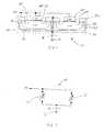
- FIG. 1is a side cross-sectional view of an embodiment of the invention showing the structure of the varactor elements
- FIG. 2is a schematic representation of FIG. 1;
- FIG. 3is a plot of the individual C-V curves of the varactor elements in FIG. 1;
- FIG. 4is a plot of the combined C-V curve of the varactor elements in FIG. 1;
- FIG. 5is a cross sectional view of an embodiment of the invention using four varactor elements
- FIG. 6is a plot of the individual C-V curves of the varactor elements of FIG. 5 .
- FIG. 7is a composite C-V curve of the four varactor elements of FIG. 6;
- FIG. 8is a cross sectional view of an alternative embodiment of the configuration of FIG. 5.
- FIG. 9is an alternative embodiment of the varactor illustrated in FIG. 1 .
- the varactor pair 10is comprised of two varactor elements 20 , 30 .
- Varactor element 20is an n gate varactor element with an n+ doped gate contact 40 isolated from an n-well 50 by an n gate insulation 60 .
- the n-well 50has regions 70 which are n+ doped.
- the n-well 50is implanted in a p type substrate or body 51 .
- the n+ doped regions 70are both coupled to a voltage source 80 which is, in turn, coupled to ground 90 .
- the varactor element 30is p gate varactor element with a structure generally similar to that of the varactor element 20 .
- the varactor element 30also has, similar to varactor 20 , an n-well 50 and n+ doped regions 70 .
- Varactor element 30also has an n gate insulator 100 which electrically isolates the body 50 from a p+ type gate contact 110 .
- the construction of the varactor elements 20 and 30are generally similar except for the gate contacts 40 and 110 .
- the gate contacts, 40 , 110are both coupled to the output OUT while all the n+ doped regions 70 are coupled together to the voltage source 80 .
- FIG. 2a schematic diagram shows the general interconnections and circuit equivalents of FIG. 1 .
- the varactor 10is essentially two varactor elements 20 , 30 which are coupled in parallel and which are further coupled to a voltage source 80 .
- C-V curvesThe capacitance-voltage characteristics (C-V curves) of varactor elements 20 , 30 are illustrated in FIG. 3 .
- curve 30 Acorresponds to the C-V curve for varactor element 30
- curve 20 Acorresponds to the C-V curve for varactor element 20 .
- the C-V curves of each of the varactor elementsare identical but shifted in voltage. This is accomplished because the n+ and p+ gates (respectively 40 , 110 ) have different contact potentials, ⁇ MS to the n-well 50 .
- the shiftcan be related by the difference in flatband voltage, V fb (as indicated in FIG. 3) of the two structures.
- V fbP⁇ MSP ⁇ Q f C ox + V tadjP Eqn . ⁇ 2
- C oxis the gate-oxide capacitance
- Q fis the fixed oxide charge
- V tadjP and V tadjNare threshold adjust implant offsets.
- the contact potentials ⁇ MSNfor Varactor N and ⁇ MSP (for Varactor P) are ⁇ 50 mV and 1.1 V, respectively.
- ⁇ V fbV fbP ⁇ V fbN 32 1.15V.
- the shift between C-V curvesis equal to ⁇ V fb as shown in FIG. 3 .
- FIG. 4shows the sum of the C-V curves for varactor elements 20 , 30 and, as can be seen, this sum has a larger voltage control range than either varactor element separately.
- Varactor elements 20 and 30are still coupled in parallel but two new threshold adjusted varactor elements 130 , 140 have also been coupled in parallel.
- Threshold adjusted varactor elements 130 , 140are similar in structure to varactor elements 20 , 30 . However, while threshold adjusted varactor element 130 is essentially an n gate varactor element, there is an important difference. Threshold adjusted varactor element 130 is a threshold adjust n gate varactor element having a threshold adjust implant 150 implanted into its n-well 50 .
- threshold adjusted varactor element 140is similar to p gate varactor element except that the threshold adjusted varactor element 140 is a threshold adjusted p gate varactor element having a threshold adjust implant 160 implanted into its n-well 50 .
- Curves 20 A and 30 Acorrespond to varactor elements 20 and 30 .
- Curves 130 A and 140 Acorrespond to varactor elements 130 and 140 .
- the equivalent capacitance of this structurethe sum of the curves 20 A, 30 A, 130 A, 140 A, is shown in FIG. 7 .
- the maximum to minimum capacitance ratiois maintained while that voltage control range is made more linear. Correct placing of the two additional curves can approximate an inverse-parabolic capacitance voltage dependence.
- V tadjNV tadjP in Eqn. 1 and Eqn. 2.
- V tadjNmust be an n type implant (e.g.
- V tadjPmust be a p type implant (e.g. boron or BF 2 ) such that the characteristics of the threshold adjusted varactor element 140 is the same as that for the varactor element 30 with a shift in the C-V curve to the right of 300 mV.
- FIG. 5is not the only one possible for adjusting the threshold of the varactor's.
- FIG. 8shows an alternative embodiment of the varactor 10 .
- channel implantsare not used on threshold adjusted varactor elements 130 , 140 . Instead, an n voltage source 170 and a p voltage source 180 are used. N voltage source 170 and p voltage source 180 are used to shift the C-V curves of threshold adjusted varactor elements 130 , and 140 respectively.
- the effect provided by the implants 150 , 160can be achieved. This approach avoids the complexity of introducing various implants and offers more flexibility in selecting the voltage range and linearity.
- FIG. 9illustrates an n type substrate implementation of the varactor pair 10 shown in FIG. 1 .
- FIG. 9is an illustration of a varactor pair 10 A comprising two varactor elements 220 , 230 .
- Varactor element 220is an n gate varactor element with an n+ doped gate contact 240 isolated from a p well 250 by an n gate insulation 260 .
- the p well 250has regions 270 which are p+ doped.
- the p well 250is implanted in an n type substrate or body 251 .
- the p+ doped regions 270are both coupled to a voltage source 80 which is, in turn coupled to ground 90 .
- Varactor element 230is a p gate varactor element with a structure generally similar to that of the varactor element 220 .
- varactor element 230has a p well 250 having p+ doped regions 270 .
- the gate insulator 300isolates the p well 250 from a p+ doped gate contact 310 .
- FIG. 9The structure illustrated in FIG. 9 can be used in much the same way as the structure pictured in FIG. 1 .
- MOS transistors with n+ and p+ gatesfor the NMOS and PMOS devices, respectively
- n+ and p+ gatesfor the NMOS and PMOS devices, respectively
- threshold adjust implantsis common in MOS processing.
- special masks to block threshold adjust implantare used to produce devices with different threshold voltages.
Landscapes
- Metal-Oxide And Bipolar Metal-Oxide Semiconductor Integrated Circuits (AREA)
- Semiconductor Integrated Circuits (AREA)
Abstract
Description


Claims (13)
Priority Applications (2)
| Application Number | Priority Date | Filing Date | Title |
|---|---|---|---|
| US09/523,592US6407412B1 (en) | 2000-03-10 | 2000-03-10 | MOS varactor structure with engineered voltage control range |
| CA002311080ACA2311080A1 (en) | 2000-03-10 | 2000-06-09 | Mos varactor structure with engineered voltage control range |
Applications Claiming Priority (1)
| Application Number | Priority Date | Filing Date | Title |
|---|---|---|---|
| US09/523,592US6407412B1 (en) | 2000-03-10 | 2000-03-10 | MOS varactor structure with engineered voltage control range |
Publications (1)
| Publication Number | Publication Date |
|---|---|
| US6407412B1true US6407412B1 (en) | 2002-06-18 |
Family
ID=24085616
Family Applications (1)
| Application Number | Title | Priority Date | Filing Date |
|---|---|---|---|
| US09/523,592Expired - LifetimeUS6407412B1 (en) | 2000-03-10 | 2000-03-10 | MOS varactor structure with engineered voltage control range |
Country Status (2)
| Country | Link |
|---|---|
| US (1) | US6407412B1 (en) |
| CA (1) | CA2311080A1 (en) |
Cited By (53)
| Publication number | Priority date | Publication date | Assignee | Title |
|---|---|---|---|---|
| US20030052389A1 (en)* | 2001-09-19 | 2003-03-20 | Mitsubishi Denki Kabushiki Kaisha | Semiconductor device including a capacitance |
| US20030085449A1 (en)* | 2001-11-08 | 2003-05-08 | International Business Machines Corporation | Method to increase the tuning voltage range of MOS varactors |
| WO2003069679A1 (en)* | 2002-02-15 | 2003-08-21 | Infineon Technologies Ag | Integrated, matchable capacitor |
| US6638841B2 (en)* | 2001-10-31 | 2003-10-28 | United Microelectronics Corp. | Method for reducing gate length bias |
| US6674333B1 (en) | 2002-10-15 | 2004-01-06 | Motorola, Inc. | Band switchable voltage controlled oscillator with substantially constant tuning range |
| US20040195643A1 (en)* | 2003-04-01 | 2004-10-07 | Texas Instruments Incorporated | Variable reactor (varactor) with engineered capacitance-voltage characteristics |
| US20050127411A1 (en)* | 2003-03-03 | 2005-06-16 | Fujitsu Limited | Mos type variable capacitance device |
| US20050184314A1 (en)* | 2004-02-25 | 2005-08-25 | Titus Ward S. | MOS varactor for LC VCOs |
| US6943399B1 (en)* | 2004-04-13 | 2005-09-13 | United Microelectronics Corp. | Varactor and differential varactor |
| US20050239260A1 (en)* | 2004-04-21 | 2005-10-27 | Bor-Min Tseng | Compensated linearity voltage-control-capacitor device by standard CMOS process |
| US20050264335A1 (en)* | 2004-05-28 | 2005-12-01 | Soe Zaw M | Digitally programmable I/Q phase offset compensation |
| US20060043454A1 (en)* | 2004-08-27 | 2006-03-02 | International Business Machines Corporation | Mos varactor using isolation well |
| US7098751B1 (en) | 2004-08-27 | 2006-08-29 | National Semiconductor Corporation | Tunable capacitance circuit for voltage control oscillator |
| WO2006063240A3 (en)* | 2004-12-09 | 2006-09-21 | Honeywell Int Inc | Varactor |
| US20070029587A1 (en)* | 2005-08-08 | 2007-02-08 | International Business Machines Corporation | Mos varactor with segmented gate doping |
| US20070252200A1 (en)* | 2004-09-08 | 2007-11-01 | Ju Jae-Ll | High voltage transistor and method for fabricating the same |
| CN100353568C (en)* | 2004-04-07 | 2007-12-05 | 联华电子股份有限公司 | Variable capacitor and differential variable capacitor |
| US20080149983A1 (en)* | 2006-12-20 | 2008-06-26 | International Business Machines Corporation | Metal-oxide-semiconductor (mos) varactors and methods of forming mos varactors |
| US20080246119A1 (en)* | 2007-04-05 | 2008-10-09 | Chartered Semiconductor Manufacturing, Ltd. | Large tuning range junction varactor |
| US20090079033A1 (en)* | 2007-09-20 | 2009-03-26 | Chartered Semiconductor Manufacturing, Ltd. | Lateral junction varactor with large tuning range |
| US20100019351A1 (en)* | 2008-07-28 | 2010-01-28 | Albert Ratnakumar | Varactors with enhanced tuning ranges |
| US20100019300A1 (en)* | 2008-06-25 | 2010-01-28 | The Trustees Of Columbia University In The City Of New York | Multilayer integrated circuit having an inductor in stacked arrangement with a distributed capacitor |
| US20120281336A1 (en)* | 2011-05-05 | 2012-11-08 | Fabio Alessio Marino | Semiconductor variable capacitor |
| US8395455B1 (en) | 2011-10-14 | 2013-03-12 | United Microelectronics Corp. | Ring oscillator |
| US8421509B1 (en) | 2011-10-25 | 2013-04-16 | United Microelectronics Corp. | Charge pump circuit with low clock feed-through |
| US8493806B1 (en) | 2012-01-03 | 2013-07-23 | United Microelectronics Corporation | Sense-amplifier circuit of memory and calibrating method thereof |
| US8588020B2 (en) | 2011-11-16 | 2013-11-19 | United Microelectronics Corporation | Sense amplifier and method for determining values of voltages on bit-line pair |
| US20130320421A1 (en)* | 2012-05-29 | 2013-12-05 | Kai-Ling Chiu | Metal-oxide-semiconductor capacitor |
| US8643521B1 (en) | 2012-11-28 | 2014-02-04 | United Microelectronics Corp. | Digital-to-analog converter with greater output resistance |
| US8669897B1 (en) | 2012-11-05 | 2014-03-11 | United Microelectronics Corp. | Asynchronous successive approximation register analog-to-digital converter and operating method thereof |
| US8692608B2 (en) | 2011-09-19 | 2014-04-08 | United Microelectronics Corp. | Charge pump system capable of stabilizing an output voltage |
| US8711598B1 (en) | 2012-11-21 | 2014-04-29 | United Microelectronics Corp. | Memory cell and memory cell array using the same |
| US8724404B2 (en) | 2012-10-15 | 2014-05-13 | United Microelectronics Corp. | Memory, supply voltage generation circuit, and operation method of a supply voltage generation circuit used for a memory array |
| US8866536B1 (en) | 2013-11-14 | 2014-10-21 | United Microelectronics Corp. | Process monitoring circuit and method |
| US8873295B2 (en) | 2012-11-27 | 2014-10-28 | United Microelectronics Corporation | Memory and operation method thereof |
| US20140332928A1 (en)* | 2012-05-08 | 2014-11-13 | Fabio Alessio Marino | Digital Semiconductor Variable Capacitor |
| US8917109B2 (en) | 2013-04-03 | 2014-12-23 | United Microelectronics Corporation | Method and device for pulse width estimation |
| US8947911B1 (en) | 2013-11-07 | 2015-02-03 | United Microelectronics Corp. | Method and circuit for optimizing bit line power consumption |
| US8953401B2 (en) | 2012-12-07 | 2015-02-10 | United Microelectronics Corp. | Memory device and method for driving memory array thereof |
| US8970197B2 (en) | 2012-08-03 | 2015-03-03 | United Microelectronics Corporation | Voltage regulating circuit configured to have output voltage thereof modulated digitally |
| US9030221B2 (en) | 2011-09-20 | 2015-05-12 | United Microelectronics Corporation | Circuit structure of test-key and test method thereof |
| US9030886B2 (en) | 2012-12-07 | 2015-05-12 | United Microelectronics Corp. | Memory device and driving method thereof |
| US20150194538A1 (en)* | 2011-05-05 | 2015-07-09 | Eta Semiconductor Inc. | Multiple Control Transcap Variable Capacitor |
| US9105355B2 (en) | 2013-07-04 | 2015-08-11 | United Microelectronics Corporation | Memory cell array operated with multiple operation voltage |
| US9143143B2 (en) | 2014-01-13 | 2015-09-22 | United Microelectronics Corp. | VCO restart up circuit and method thereof |
| US9236466B1 (en) | 2011-10-07 | 2016-01-12 | Mie Fujitsu Semiconductor Limited | Analog circuits having improved insulated gate transistors, and methods therefor |
| US9299699B2 (en) | 2013-03-13 | 2016-03-29 | Taiwan Semiconductor Manufacturing Company, Ltd. | Multi-gate and complementary varactors in FinFET process |
| WO2016165627A1 (en)* | 2015-04-15 | 2016-10-20 | Huawei Technologies Co., Ltd. | Apparatus and method for low loss coupling capacitor |
| CN106206259A (en)* | 2016-08-30 | 2016-12-07 | 上海华力微电子有限公司 | A kind of method reducing variodenser minimum capacity |
| US9614107B2 (en) | 2011-11-08 | 2017-04-04 | International Business Machines Corporation | Quantum capacitance graphene varactors and fabrication methods |
| CN109411488A (en)* | 2017-08-15 | 2019-03-01 | 台湾积体电路制造股份有限公司 | A kind of semiconductor devices and forming method thereof |
| US20190158021A1 (en)* | 2017-11-22 | 2019-05-23 | Seiko Epson Corporation | Temperature-compensated crystal oscillator, and electronic device using the same |
| US11380679B2 (en)* | 2018-09-25 | 2022-07-05 | Intel Corporation | FET capacitor circuit architectures for tunable load and input matching |
Citations (6)
| Publication number | Priority date | Publication date | Assignee | Title |
|---|---|---|---|---|
| US5159426A (en)* | 1988-04-29 | 1992-10-27 | Dallas Semiconductor Corporation | Integrated circuit with improved battery protection |
| US5864158A (en)* | 1997-04-04 | 1999-01-26 | Advanced Micro Devices, Inc. | Trench-gated vertical CMOS device |
| US6100770A (en)* | 1997-09-11 | 2000-08-08 | Telefonaktiebolaget Lm Ericsson (Publ) | MIS transistor varactor device and oscillator using same |
| US6211745B1 (en)* | 1999-05-03 | 2001-04-03 | Silicon Wave, Inc. | Method and apparatus for digitally controlling the capacitance of an integrated circuit device using mos-field effect transistors |
| US6218703B1 (en)* | 1995-07-23 | 2001-04-17 | Ricoh Company, Ltd. | Semiconductor device with control electrodes formed from semiconductor material |
| US6268778B1 (en)* | 1999-05-03 | 2001-07-31 | Silicon Wave, Inc. | Method and apparatus for fully integrating a voltage controlled oscillator on an integrated circuit |
- 2000
- 2000-03-10USUS09/523,592patent/US6407412B1/ennot_activeExpired - Lifetime
- 2000-06-09CACA002311080Apatent/CA2311080A1/ennot_activeAbandoned
Patent Citations (6)
| Publication number | Priority date | Publication date | Assignee | Title |
|---|---|---|---|---|
| US5159426A (en)* | 1988-04-29 | 1992-10-27 | Dallas Semiconductor Corporation | Integrated circuit with improved battery protection |
| US6218703B1 (en)* | 1995-07-23 | 2001-04-17 | Ricoh Company, Ltd. | Semiconductor device with control electrodes formed from semiconductor material |
| US5864158A (en)* | 1997-04-04 | 1999-01-26 | Advanced Micro Devices, Inc. | Trench-gated vertical CMOS device |
| US6100770A (en)* | 1997-09-11 | 2000-08-08 | Telefonaktiebolaget Lm Ericsson (Publ) | MIS transistor varactor device and oscillator using same |
| US6211745B1 (en)* | 1999-05-03 | 2001-04-03 | Silicon Wave, Inc. | Method and apparatus for digitally controlling the capacitance of an integrated circuit device using mos-field effect transistors |
| US6268778B1 (en)* | 1999-05-03 | 2001-07-31 | Silicon Wave, Inc. | Method and apparatus for fully integrating a voltage controlled oscillator on an integrated circuit |
Cited By (92)
| Publication number | Priority date | Publication date | Assignee | Title |
|---|---|---|---|---|
| US6858918B2 (en)* | 2001-09-19 | 2005-02-22 | Renesas Technology Corp. | Semiconductor device including a capacitance |
| US7608879B2 (en) | 2001-09-19 | 2009-10-27 | Renesas Technology Corp. | Semiconductor device including a capacitance |
| US7339238B2 (en) | 2001-09-19 | 2008-03-04 | Renesas Technology Corp. | Semiconductor device including a capacitance |
| US20030052389A1 (en)* | 2001-09-19 | 2003-03-20 | Mitsubishi Denki Kabushiki Kaisha | Semiconductor device including a capacitance |
| US20050087779A1 (en)* | 2001-09-19 | 2005-04-28 | Renesas Technology Corp. | Semiconductor device including a capacitance |
| US20060289906A1 (en)* | 2001-09-19 | 2006-12-28 | Renesas Technology Corp. | Semiconductor device including a capacitance |
| US7112835B2 (en) | 2001-09-19 | 2006-09-26 | Renesas Technology Corp. | Semiconductor device including a capacitance |
| US20070296009A1 (en)* | 2001-09-19 | 2007-12-27 | Renesas Technology Corp. | Semiconductor device including a capacitance |
| US6638841B2 (en)* | 2001-10-31 | 2003-10-28 | United Microelectronics Corp. | Method for reducing gate length bias |
| US6667539B2 (en)* | 2001-11-08 | 2003-12-23 | International Business Machines Corporation | Method to increase the tuning voltage range of MOS varactors |
| US20030085449A1 (en)* | 2001-11-08 | 2003-05-08 | International Business Machines Corporation | Method to increase the tuning voltage range of MOS varactors |
| US20050067674A1 (en)* | 2002-02-15 | 2005-03-31 | Judith Maget | Integrated tuneable capacitance |
| WO2003069679A1 (en)* | 2002-02-15 | 2003-08-21 | Infineon Technologies Ag | Integrated, matchable capacitor |
| US6674333B1 (en) | 2002-10-15 | 2004-01-06 | Motorola, Inc. | Band switchable voltage controlled oscillator with substantially constant tuning range |
| US7622760B2 (en) | 2003-03-03 | 2009-11-24 | Fujitsu Microelectronics Limited | MOS type variable capacitance device |
| US20050127411A1 (en)* | 2003-03-03 | 2005-06-16 | Fujitsu Limited | Mos type variable capacitance device |
| EP1553636A4 (en)* | 2003-03-03 | 2006-08-30 | Fujitsu Ltd | CAPACITIVE DEVICE WITH VARIABLE MOS |
| US6847095B2 (en) | 2003-04-01 | 2005-01-25 | Texas Instruments Incorporated | Variable reactor (varactor) with engineered capacitance-voltage characteristics |
| US20040195643A1 (en)* | 2003-04-01 | 2004-10-07 | Texas Instruments Incorporated | Variable reactor (varactor) with engineered capacitance-voltage characteristics |
| US20050184314A1 (en)* | 2004-02-25 | 2005-08-25 | Titus Ward S. | MOS varactor for LC VCOs |
| US7038527B2 (en) | 2004-02-25 | 2006-05-02 | Analog Devices, Inc. | MOS varactor for LC VCOs |
| CN100353568C (en)* | 2004-04-07 | 2007-12-05 | 联华电子股份有限公司 | Variable capacitor and differential variable capacitor |
| US6943399B1 (en)* | 2004-04-13 | 2005-09-13 | United Microelectronics Corp. | Varactor and differential varactor |
| US7223667B2 (en) | 2004-04-21 | 2007-05-29 | Taiwan Semiconductor Manufacturing Company, Ltd. | Compensated linearity voltage-control-capacitor device by standard CMOS process |
| US20050239260A1 (en)* | 2004-04-21 | 2005-10-27 | Bor-Min Tseng | Compensated linearity voltage-control-capacitor device by standard CMOS process |
| US7068089B2 (en)* | 2004-05-28 | 2006-06-27 | Wionics Research | Digitally programmable I/Q phase offset compensation |
| US20050264335A1 (en)* | 2004-05-28 | 2005-12-01 | Soe Zaw M | Digitally programmable I/Q phase offset compensation |
| US7098751B1 (en) | 2004-08-27 | 2006-08-29 | National Semiconductor Corporation | Tunable capacitance circuit for voltage control oscillator |
| US7714412B2 (en) | 2004-08-27 | 2010-05-11 | International Business Machines Corporation | MOS varactor using isolation well |
| US20060043454A1 (en)* | 2004-08-27 | 2006-03-02 | International Business Machines Corporation | Mos varactor using isolation well |
| US20070252200A1 (en)* | 2004-09-08 | 2007-11-01 | Ju Jae-Ll | High voltage transistor and method for fabricating the same |
| US7531872B2 (en)* | 2004-09-08 | 2009-05-12 | Magnachip Semiconductor, Ltd. | High voltage transistor and method for fabricating the same |
| WO2006063240A3 (en)* | 2004-12-09 | 2006-09-21 | Honeywell Int Inc | Varactor |
| US20070029587A1 (en)* | 2005-08-08 | 2007-02-08 | International Business Machines Corporation | Mos varactor with segmented gate doping |
| US7545007B2 (en) | 2005-08-08 | 2009-06-09 | International Business Machines Corporation | MOS varactor with segmented gate doping |
| US20080149983A1 (en)* | 2006-12-20 | 2008-06-26 | International Business Machines Corporation | Metal-oxide-semiconductor (mos) varactors and methods of forming mos varactors |
| US20080246119A1 (en)* | 2007-04-05 | 2008-10-09 | Chartered Semiconductor Manufacturing, Ltd. | Large tuning range junction varactor |
| US8450832B2 (en) | 2007-04-05 | 2013-05-28 | Globalfoundries Singapore Pte. Ltd. | Large tuning range junction varactor |
| US20090079033A1 (en)* | 2007-09-20 | 2009-03-26 | Chartered Semiconductor Manufacturing, Ltd. | Lateral junction varactor with large tuning range |
| US7952131B2 (en) | 2007-09-20 | 2011-05-31 | Chartered Semiconductor Manufacturing, Ltd. | Lateral junction varactor with large tuning range |
| US20100258910A1 (en)* | 2007-09-20 | 2010-10-14 | Globalfoundries Singapore Pte. Ltd. | Lateral junction varactor with large tuning range |
| US7741187B2 (en) | 2007-09-20 | 2010-06-22 | Chartered Semiconductor Manufacturing, Ltd. | Lateral junction varactor with large tuning range |
| US20100019300A1 (en)* | 2008-06-25 | 2010-01-28 | The Trustees Of Columbia University In The City Of New York | Multilayer integrated circuit having an inductor in stacked arrangement with a distributed capacitor |
| WO2010014355A3 (en)* | 2008-07-28 | 2010-04-08 | Altera Corporation | Varactors with enhanced tuning ranges |
| CN102165597A (en)* | 2008-07-28 | 2011-08-24 | 阿尔特拉公司 | Varactors with enhanced tuning ranges |
| US20100019351A1 (en)* | 2008-07-28 | 2010-01-28 | Albert Ratnakumar | Varactors with enhanced tuning ranges |
| US20120281336A1 (en)* | 2011-05-05 | 2012-11-08 | Fabio Alessio Marino | Semiconductor variable capacitor |
| US9401436B2 (en)* | 2011-05-05 | 2016-07-26 | Qualcomm Incorporated | Multiple control transcap variable capacitor |
| US8498094B2 (en)* | 2011-05-05 | 2013-07-30 | Eta Semiconductor Inc. | Semiconductor variable capacitor |
| US20150194538A1 (en)* | 2011-05-05 | 2015-07-09 | Eta Semiconductor Inc. | Multiple Control Transcap Variable Capacitor |
| US8692608B2 (en) | 2011-09-19 | 2014-04-08 | United Microelectronics Corp. | Charge pump system capable of stabilizing an output voltage |
| US9030221B2 (en) | 2011-09-20 | 2015-05-12 | United Microelectronics Corporation | Circuit structure of test-key and test method thereof |
| US9236466B1 (en) | 2011-10-07 | 2016-01-12 | Mie Fujitsu Semiconductor Limited | Analog circuits having improved insulated gate transistors, and methods therefor |
| US8395455B1 (en) | 2011-10-14 | 2013-03-12 | United Microelectronics Corp. | Ring oscillator |
| US8421509B1 (en) | 2011-10-25 | 2013-04-16 | United Microelectronics Corp. | Charge pump circuit with low clock feed-through |
| US9893212B2 (en) | 2011-11-08 | 2018-02-13 | International Business Machines Corporation | Quantum capacitance graphene varactors and fabrication methods |
| US9614107B2 (en) | 2011-11-08 | 2017-04-04 | International Business Machines Corporation | Quantum capacitance graphene varactors and fabrication methods |
| US11024750B2 (en) | 2011-11-08 | 2021-06-01 | International Business Machines Corporation | Quantum capacitance graphene varactors and fabrication methods |
| US10636917B2 (en) | 2011-11-08 | 2020-04-28 | International Business Machines Corporation | Quantum capacitance graphene varactors and fabrication methods |
| US8588020B2 (en) | 2011-11-16 | 2013-11-19 | United Microelectronics Corporation | Sense amplifier and method for determining values of voltages on bit-line pair |
| US8493806B1 (en) | 2012-01-03 | 2013-07-23 | United Microelectronics Corporation | Sense-amplifier circuit of memory and calibrating method thereof |
| US8963289B2 (en)* | 2012-05-08 | 2015-02-24 | Eta Semiconductor Inc. | Digital semiconductor variable capacitor |
| US20140332928A1 (en)* | 2012-05-08 | 2014-11-13 | Fabio Alessio Marino | Digital Semiconductor Variable Capacitor |
| US8664705B2 (en)* | 2012-05-29 | 2014-03-04 | United Microelectronics Corp. | Metal-oxide-semiconductor capacitor |
| US20130320421A1 (en)* | 2012-05-29 | 2013-12-05 | Kai-Ling Chiu | Metal-oxide-semiconductor capacitor |
| US8970197B2 (en) | 2012-08-03 | 2015-03-03 | United Microelectronics Corporation | Voltage regulating circuit configured to have output voltage thereof modulated digitally |
| US8804440B1 (en) | 2012-10-15 | 2014-08-12 | United Microelectronics Corporation | Memory for a voltage regulator circuit |
| US8767485B1 (en) | 2012-10-15 | 2014-07-01 | United Microelectronics Corp. | Operation method of a supply voltage generation circuit used for a memory array |
| US8724404B2 (en) | 2012-10-15 | 2014-05-13 | United Microelectronics Corp. | Memory, supply voltage generation circuit, and operation method of a supply voltage generation circuit used for a memory array |
| US8669897B1 (en) | 2012-11-05 | 2014-03-11 | United Microelectronics Corp. | Asynchronous successive approximation register analog-to-digital converter and operating method thereof |
| US8711598B1 (en) | 2012-11-21 | 2014-04-29 | United Microelectronics Corp. | Memory cell and memory cell array using the same |
| US8873295B2 (en) | 2012-11-27 | 2014-10-28 | United Microelectronics Corporation | Memory and operation method thereof |
| US8643521B1 (en) | 2012-11-28 | 2014-02-04 | United Microelectronics Corp. | Digital-to-analog converter with greater output resistance |
| US8953401B2 (en) | 2012-12-07 | 2015-02-10 | United Microelectronics Corp. | Memory device and method for driving memory array thereof |
| US9030886B2 (en) | 2012-12-07 | 2015-05-12 | United Microelectronics Corp. | Memory device and driving method thereof |
| US9299699B2 (en) | 2013-03-13 | 2016-03-29 | Taiwan Semiconductor Manufacturing Company, Ltd. | Multi-gate and complementary varactors in FinFET process |
| US9698146B2 (en) | 2013-03-13 | 2017-07-04 | Taiwan Semiconductor Manufacturing Company, Ltd. | Multi-gate and complementary varactors in FinFET process |
| US8917109B2 (en) | 2013-04-03 | 2014-12-23 | United Microelectronics Corporation | Method and device for pulse width estimation |
| US9105355B2 (en) | 2013-07-04 | 2015-08-11 | United Microelectronics Corporation | Memory cell array operated with multiple operation voltage |
| US8947911B1 (en) | 2013-11-07 | 2015-02-03 | United Microelectronics Corp. | Method and circuit for optimizing bit line power consumption |
| US8866536B1 (en) | 2013-11-14 | 2014-10-21 | United Microelectronics Corp. | Process monitoring circuit and method |
| US9143143B2 (en) | 2014-01-13 | 2015-09-22 | United Microelectronics Corp. | VCO restart up circuit and method thereof |
| US10586878B2 (en) | 2015-04-15 | 2020-03-10 | Futurewei Technologies, Inc. | Apparatus and method for a low loss coupling capacitor |
| US9837555B2 (en) | 2015-04-15 | 2017-12-05 | Futurewei Technologies, Inc. | Apparatus and method for a low loss coupling capacitor |
| WO2016165627A1 (en)* | 2015-04-15 | 2016-10-20 | Huawei Technologies Co., Ltd. | Apparatus and method for low loss coupling capacitor |
| US11569393B2 (en) | 2015-04-15 | 2023-01-31 | Futurewei Technologies, Inc. | Apparatus and method for a low loss coupling capacitor |
| CN106206259A (en)* | 2016-08-30 | 2016-12-07 | 上海华力微电子有限公司 | A kind of method reducing variodenser minimum capacity |
| CN106206259B (en)* | 2016-08-30 | 2019-05-31 | 上海华力微电子有限公司 | A method of reducing variodenser minimum capacity |
| CN109411488A (en)* | 2017-08-15 | 2019-03-01 | 台湾积体电路制造股份有限公司 | A kind of semiconductor devices and forming method thereof |
| CN109411488B (en)* | 2017-08-15 | 2021-09-10 | 台湾积体电路制造股份有限公司 | Semiconductor device and forming method thereof |
| US20190158021A1 (en)* | 2017-11-22 | 2019-05-23 | Seiko Epson Corporation | Temperature-compensated crystal oscillator, and electronic device using the same |
| US11380679B2 (en)* | 2018-09-25 | 2022-07-05 | Intel Corporation | FET capacitor circuit architectures for tunable load and input matching |
Also Published As
| Publication number | Publication date |
|---|---|
| CA2311080A1 (en) | 2001-09-10 |
Similar Documents
| Publication | Publication Date | Title |
|---|---|---|
| US6407412B1 (en) | MOS varactor structure with engineered voltage control range | |
| US8809835B2 (en) | RF circuits including transistors having strained material layers | |
| KR100682286B1 (en) | Linear Capacitor Structure in CMOS Processing | |
| US8143936B2 (en) | Application of control signal and forward body-bias signal to an active device | |
| AU9192498A (en) | Electrical devices and a method of manufacturing the same | |
| US6621128B2 (en) | Method of fabricating a MOS capacitor | |
| US7078787B1 (en) | Design and operation of gate-enhanced junction varactor with gradual capacitance variation | |
| US5565375A (en) | Method of fabricating a self-cascoding CMOS device | |
| EP1553636B1 (en) | Mos variable capacitive device | |
| US6514824B1 (en) | Semiconductor device with a pair of transistors having dual work function gate electrodes | |
| US20010015449A1 (en) | Semiconductor - oxide - semiconductor capacitor formed in intergtated circuit | |
| US20040082124A1 (en) | High performance varactor diodes | |
| US6600205B2 (en) | Method for making low voltage transistors with increased breakdown voltage to substrate having three different MOS transistors | |
| US7223667B2 (en) | Compensated linearity voltage-control-capacitor device by standard CMOS process | |
| US6653716B1 (en) | Varactor and method of forming a varactor with an increased linear tuning range | |
| US6847095B2 (en) | Variable reactor (varactor) with engineered capacitance-voltage characteristics | |
| EP1981087B1 (en) | Electrical device comprising a voltage dependant capacitance and method for manufacturing the same | |
| US20050067674A1 (en) | Integrated tuneable capacitance | |
| DE69708147T2 (en) | NNN / PPP LOGICAL ARRANGEMENTS WITH ULTRA-LOW PERFORMANCE DELAY PRODUCT | |
| WO1993013547A2 (en) | Integrated circuit | |
| US6825546B1 (en) | CMOS varactor with constant dC/dV characteristic | |
| EP0616725A1 (en) | Electrical isolation in integrated circuits | |
| US20040067600A1 (en) | Reduced gate leakage current in thin gate dielectric CMOS integrated circuits | |
| DE69027312T2 (en) | FIELD EFFECT TRANSISTOR WITH FERMI THRESHOLD VOLTAGE | |
| DE10139396A1 (en) | Integrated circuit with a varactor for a voltage controlled oscillator has source and drain implants outside gate joined by homogeneously doped substrate region |
Legal Events
| Date | Code | Title | Description |
|---|---|---|---|
| AS | Assignment | Owner name:PMC-SIERRA INC., CANADA Free format text:ASSIGNMENT OF ASSIGNORS INTEREST;ASSIGNORS:INIEWSKI, KRZYSZTOF;MAGIEROWSKI, SEBASTIAN CLAUDIUSZ;REEL/FRAME:010670/0904;SIGNING DATES FROM 20000215 TO 20000229 | |
| STCF | Information on status: patent grant | Free format text:PATENTED CASE | |
| FEPP | Fee payment procedure | Free format text:PAYOR NUMBER ASSIGNED (ORIGINAL EVENT CODE: ASPN); ENTITY STATUS OF PATENT OWNER: LARGE ENTITY Free format text:PAYER NUMBER DE-ASSIGNED (ORIGINAL EVENT CODE: RMPN); ENTITY STATUS OF PATENT OWNER: LARGE ENTITY | |
| FPAY | Fee payment | Year of fee payment:4 | |
| FPAY | Fee payment | Year of fee payment:8 | |
| AS | Assignment | Owner name:BANK OF AMERICA, N.A., NORTH CAROLINA Free format text:SECURITY INTEREST IN PATENTS;ASSIGNORS:PMC-SIERRA, INC.;PMC-SIERRA US, INC.;WINTEGRA, INC.;REEL/FRAME:030947/0710 Effective date:20130802 | |
| FPAY | Fee payment | Year of fee payment:12 | |
| AS | Assignment | Owner name:PMC-SIERRA US, INC., CALIFORNIA Free format text:RELEASE BY SECURED PARTY;ASSIGNOR:BANK OF AMERICA, N.A.;REEL/FRAME:037675/0129 Effective date:20160115 Owner name:WINTEGRA, INC., CALIFORNIA Free format text:RELEASE BY SECURED PARTY;ASSIGNOR:BANK OF AMERICA, N.A.;REEL/FRAME:037675/0129 Effective date:20160115 Owner name:PMC-SIERRA, INC., CALIFORNIA Free format text:RELEASE BY SECURED PARTY;ASSIGNOR:BANK OF AMERICA, N.A.;REEL/FRAME:037675/0129 Effective date:20160115 | |
| AS | Assignment | Owner name:MORGAN STANLEY SENIOR FUNDING, INC., NEW YORK Free format text:PATENT SECURITY AGREEMENT;ASSIGNORS:MICROSEMI STORAGE SOLUTIONS, INC. (F/K/A PMC-SIERRA, INC.);MICROSEMI STORAGE SOLUTIONS (U.S.), INC. (F/K/A PMC-SIERRA US, INC.);REEL/FRAME:037689/0719 Effective date:20160115 | |
| AS | Assignment | Owner name:MICROSEMI STORAGE SOLUTIONS (U.S.), INC., CALIFORN Free format text:RELEASE BY SECURED PARTY;ASSIGNOR:MORGAN STANLEY SENIOR FUNDING, INC.;REEL/FRAME:046251/0271 Effective date:20180529 Owner name:MICROSEMI STORAGE SOLUTIONS, INC., CALIFORNIA Free format text:RELEASE BY SECURED PARTY;ASSIGNOR:MORGAN STANLEY SENIOR FUNDING, INC.;REEL/FRAME:046251/0271 Effective date:20180529 | |
| AS | Assignment | Owner name:JPMORGAN CHASE BANK, N.A., AS ADMINISTRATIVE AGENT, ILLINOIS Free format text:SECURITY INTEREST;ASSIGNORS:MICROCHIP TECHNOLOGY INCORPORATED;SILICON STORAGE TECHNOLOGY, INC.;ATMEL CORPORATION;AND OTHERS;REEL/FRAME:046426/0001 Effective date:20180529 Owner name:JPMORGAN CHASE BANK, N.A., AS ADMINISTRATIVE AGENT Free format text:SECURITY INTEREST;ASSIGNORS:MICROCHIP TECHNOLOGY INCORPORATED;SILICON STORAGE TECHNOLOGY, INC.;ATMEL CORPORATION;AND OTHERS;REEL/FRAME:046426/0001 Effective date:20180529 | |
| AS | Assignment | Owner name:WELLS FARGO BANK, NATIONAL ASSOCIATION, AS NOTES COLLATERAL AGENT, CALIFORNIA Free format text:SECURITY INTEREST;ASSIGNORS:MICROCHIP TECHNOLOGY INCORPORATED;SILICON STORAGE TECHNOLOGY, INC.;ATMEL CORPORATION;AND OTHERS;REEL/FRAME:047103/0206 Effective date:20180914 Owner name:WELLS FARGO BANK, NATIONAL ASSOCIATION, AS NOTES C Free format text:SECURITY INTEREST;ASSIGNORS:MICROCHIP TECHNOLOGY INCORPORATED;SILICON STORAGE TECHNOLOGY, INC.;ATMEL CORPORATION;AND OTHERS;REEL/FRAME:047103/0206 Effective date:20180914 | |
| AS | Assignment | Owner name:JPMORGAN CHASE BANK, N.A., AS ADMINISTRATIVE AGENT, DELAWARE Free format text:SECURITY INTEREST;ASSIGNORS:MICROCHIP TECHNOLOGY INC.;SILICON STORAGE TECHNOLOGY, INC.;ATMEL CORPORATION;AND OTHERS;REEL/FRAME:053311/0305 Effective date:20200327 | |
| AS | Assignment | Owner name:ATMEL CORPORATION, ARIZONA Free format text:RELEASE BY SECURED PARTY;ASSIGNOR:JPMORGAN CHASE BANK, N.A, AS ADMINISTRATIVE AGENT;REEL/FRAME:053466/0011 Effective date:20200529 Owner name:MICROSEMI STORAGE SOLUTIONS, INC., ARIZONA Free format text:RELEASE BY SECURED PARTY;ASSIGNOR:JPMORGAN CHASE BANK, N.A, AS ADMINISTRATIVE AGENT;REEL/FRAME:053466/0011 Effective date:20200529 Owner name:MICROSEMI CORPORATION, CALIFORNIA Free format text:RELEASE BY SECURED PARTY;ASSIGNOR:JPMORGAN CHASE BANK, N.A, AS ADMINISTRATIVE AGENT;REEL/FRAME:053466/0011 Effective date:20200529 Owner name:MICROCHIP TECHNOLOGY INC., ARIZONA Free format text:RELEASE BY SECURED PARTY;ASSIGNOR:JPMORGAN CHASE BANK, N.A, AS ADMINISTRATIVE AGENT;REEL/FRAME:053466/0011 Effective date:20200529 Owner name:SILICON STORAGE TECHNOLOGY, INC., ARIZONA Free format text:RELEASE BY SECURED PARTY;ASSIGNOR:JPMORGAN CHASE BANK, N.A, AS ADMINISTRATIVE AGENT;REEL/FRAME:053466/0011 Effective date:20200529 | |
| AS | Assignment | Owner name:WELLS FARGO BANK, NATIONAL ASSOCIATION, MINNESOTA Free format text:SECURITY INTEREST;ASSIGNORS:MICROCHIP TECHNOLOGY INC.;SILICON STORAGE TECHNOLOGY, INC.;ATMEL CORPORATION;AND OTHERS;REEL/FRAME:053468/0705 Effective date:20200529 | |
| AS | Assignment | Owner name:WELLS FARGO BANK, NATIONAL ASSOCIATION, AS COLLATERAL AGENT, MINNESOTA Free format text:SECURITY INTEREST;ASSIGNORS:MICROCHIP TECHNOLOGY INCORPORATED;SILICON STORAGE TECHNOLOGY, INC.;ATMEL CORPORATION;AND OTHERS;REEL/FRAME:055671/0612 Effective date:20201217 | |
| AS | Assignment | Owner name:MICROSEMI STORAGE SOLUTIONS, INC., ARIZONA Free format text:RELEASE BY SECURED PARTY;ASSIGNOR:JPMORGAN CHASE BANK, N.A., AS ADMINISTRATIVE AGENT;REEL/FRAME:059333/0222 Effective date:20220218 Owner name:MICROSEMI CORPORATION, ARIZONA Free format text:RELEASE BY SECURED PARTY;ASSIGNOR:JPMORGAN CHASE BANK, N.A., AS ADMINISTRATIVE AGENT;REEL/FRAME:059333/0222 Effective date:20220218 Owner name:ATMEL CORPORATION, ARIZONA Free format text:RELEASE BY SECURED PARTY;ASSIGNOR:JPMORGAN CHASE BANK, N.A., AS ADMINISTRATIVE AGENT;REEL/FRAME:059333/0222 Effective date:20220218 Owner name:SILICON STORAGE TECHNOLOGY, INC., ARIZONA Free format text:RELEASE BY SECURED PARTY;ASSIGNOR:JPMORGAN CHASE BANK, N.A., AS ADMINISTRATIVE AGENT;REEL/FRAME:059333/0222 Effective date:20220218 Owner name:MICROCHIP TECHNOLOGY INCORPORATED, ARIZONA Free format text:RELEASE BY SECURED PARTY;ASSIGNOR:JPMORGAN CHASE BANK, N.A., AS ADMINISTRATIVE AGENT;REEL/FRAME:059333/0222 Effective date:20220218 | |
| AS | Assignment | Owner name:MICROSEMI STORAGE SOLUTIONS, INC., ARIZONA Free format text:RELEASE BY SECURED PARTY;ASSIGNOR:WELLS FARGO BANK, NATIONAL ASSOCIATION, AS NOTES COLLATERAL AGENT;REEL/FRAME:059358/0001 Effective date:20220228 Owner name:MICROSEMI CORPORATION, ARIZONA Free format text:RELEASE BY SECURED PARTY;ASSIGNOR:WELLS FARGO BANK, NATIONAL ASSOCIATION, AS NOTES COLLATERAL AGENT;REEL/FRAME:059358/0001 Effective date:20220228 Owner name:ATMEL CORPORATION, ARIZONA Free format text:RELEASE BY SECURED PARTY;ASSIGNOR:WELLS FARGO BANK, NATIONAL ASSOCIATION, AS NOTES COLLATERAL AGENT;REEL/FRAME:059358/0001 Effective date:20220228 Owner name:SILICON STORAGE TECHNOLOGY, INC., ARIZONA Free format text:RELEASE BY SECURED PARTY;ASSIGNOR:WELLS FARGO BANK, NATIONAL ASSOCIATION, AS NOTES COLLATERAL AGENT;REEL/FRAME:059358/0001 Effective date:20220228 Owner name:MICROCHIP TECHNOLOGY INCORPORATED, ARIZONA Free format text:RELEASE BY SECURED PARTY;ASSIGNOR:WELLS FARGO BANK, NATIONAL ASSOCIATION, AS NOTES COLLATERAL AGENT;REEL/FRAME:059358/0001 Effective date:20220228 | |
| AS | Assignment | Owner name:MICROSEMI STORAGE SOLUTIONS, INC., ARIZONA Free format text:RELEASE BY SECURED PARTY;ASSIGNOR:WELLS FARGO BANK, NATIONAL ASSOCIATION, AS NOTES COLLATERAL AGENT;REEL/FRAME:059863/0400 Effective date:20220228 Owner name:MICROSEMI CORPORATION, ARIZONA Free format text:RELEASE BY SECURED PARTY;ASSIGNOR:WELLS FARGO BANK, NATIONAL ASSOCIATION, AS NOTES COLLATERAL AGENT;REEL/FRAME:059863/0400 Effective date:20220228 Owner name:ATMEL CORPORATION, ARIZONA Free format text:RELEASE BY SECURED PARTY;ASSIGNOR:WELLS FARGO BANK, NATIONAL ASSOCIATION, AS NOTES COLLATERAL AGENT;REEL/FRAME:059863/0400 Effective date:20220228 Owner name:SILICON STORAGE TECHNOLOGY, INC., ARIZONA Free format text:RELEASE BY SECURED PARTY;ASSIGNOR:WELLS FARGO BANK, NATIONAL ASSOCIATION, AS NOTES COLLATERAL AGENT;REEL/FRAME:059863/0400 Effective date:20220228 Owner name:MICROCHIP TECHNOLOGY INCORPORATED, ARIZONA Free format text:RELEASE BY SECURED PARTY;ASSIGNOR:WELLS FARGO BANK, NATIONAL ASSOCIATION, AS NOTES COLLATERAL AGENT;REEL/FRAME:059863/0400 Effective date:20220228 | |
| AS | Assignment | Owner name:MICROSEMI STORAGE SOLUTIONS, INC., ARIZONA Free format text:RELEASE BY SECURED PARTY;ASSIGNOR:WELLS FARGO BANK, NATIONAL ASSOCIATION, AS NOTES COLLATERAL AGENT;REEL/FRAME:059363/0001 Effective date:20220228 Owner name:MICROSEMI CORPORATION, ARIZONA Free format text:RELEASE BY SECURED PARTY;ASSIGNOR:WELLS FARGO BANK, NATIONAL ASSOCIATION, AS NOTES COLLATERAL AGENT;REEL/FRAME:059363/0001 Effective date:20220228 Owner name:ATMEL CORPORATION, ARIZONA Free format text:RELEASE BY SECURED PARTY;ASSIGNOR:WELLS FARGO BANK, NATIONAL ASSOCIATION, AS NOTES COLLATERAL AGENT;REEL/FRAME:059363/0001 Effective date:20220228 Owner name:SILICON STORAGE TECHNOLOGY, INC., ARIZONA Free format text:RELEASE BY SECURED PARTY;ASSIGNOR:WELLS FARGO BANK, NATIONAL ASSOCIATION, AS NOTES COLLATERAL AGENT;REEL/FRAME:059363/0001 Effective date:20220228 Owner name:MICROCHIP TECHNOLOGY INCORPORATED, ARIZONA Free format text:RELEASE BY SECURED PARTY;ASSIGNOR:WELLS FARGO BANK, NATIONAL ASSOCIATION, AS NOTES COLLATERAL AGENT;REEL/FRAME:059363/0001 Effective date:20220228 | |
| AS | Assignment | Owner name:MICROSEMI STORAGE SOLUTIONS, INC., ARIZONA Free format text:RELEASE BY SECURED PARTY;ASSIGNOR:WELLS FARGO BANK, NATIONAL ASSOCIATION, AS NOTES COLLATERAL AGENT;REEL/FRAME:060894/0437 Effective date:20220228 Owner name:MICROSEMI CORPORATION, ARIZONA Free format text:RELEASE BY SECURED PARTY;ASSIGNOR:WELLS FARGO BANK, NATIONAL ASSOCIATION, AS NOTES COLLATERAL AGENT;REEL/FRAME:060894/0437 Effective date:20220228 Owner name:ATMEL CORPORATION, ARIZONA Free format text:RELEASE BY SECURED PARTY;ASSIGNOR:WELLS FARGO BANK, NATIONAL ASSOCIATION, AS NOTES COLLATERAL AGENT;REEL/FRAME:060894/0437 Effective date:20220228 Owner name:SILICON STORAGE TECHNOLOGY, INC., ARIZONA Free format text:RELEASE BY SECURED PARTY;ASSIGNOR:WELLS FARGO BANK, NATIONAL ASSOCIATION, AS NOTES COLLATERAL AGENT;REEL/FRAME:060894/0437 Effective date:20220228 Owner name:MICROCHIP TECHNOLOGY INCORPORATED, ARIZONA Free format text:RELEASE BY SECURED PARTY;ASSIGNOR:WELLS FARGO BANK, NATIONAL ASSOCIATION, AS NOTES COLLATERAL AGENT;REEL/FRAME:060894/0437 Effective date:20220228 |