US6406555B1 - Point of use dilution tool and method - Google Patents
Point of use dilution tool and methodDownload PDFInfo
- Publication number
- US6406555B1 US6406555B1US09/495,180US49518000AUS6406555B1US 6406555 B1US6406555 B1US 6406555B1US 49518000 AUS49518000 AUS 49518000AUS 6406555 B1US6406555 B1US 6406555B1
- Authority
- US
- United States
- Prior art keywords
- solution
- fluid
- filter
- flow rate
- wafer
- Prior art date
- Legal status (The legal status is an assumption and is not a legal conclusion. Google has not performed a legal analysis and makes no representation as to the accuracy of the status listed.)
- Expired - Lifetime
Links
Images

Classifications
- H—ELECTRICITY
- H01—ELECTRIC ELEMENTS
- H01L—SEMICONDUCTOR DEVICES NOT COVERED BY CLASS H10
- H01L21/00—Processes or apparatus adapted for the manufacture or treatment of semiconductor or solid state devices or of parts thereof
- H01L21/67—Apparatus specially adapted for handling semiconductor or electric solid state devices during manufacture or treatment thereof; Apparatus specially adapted for handling wafers during manufacture or treatment of semiconductor or electric solid state devices or components ; Apparatus not specifically provided for elsewhere
- H01L21/67005—Apparatus not specifically provided for elsewhere
- H01L21/67011—Apparatus for manufacture or treatment
- H01L21/67017—Apparatus for fluid treatment
- H01L21/67028—Apparatus for fluid treatment for cleaning followed by drying, rinsing, stripping, blasting or the like
- H—ELECTRICITY
- H01—ELECTRIC ELEMENTS
- H01L—SEMICONDUCTOR DEVICES NOT COVERED BY CLASS H10
- H01L21/00—Processes or apparatus adapted for the manufacture or treatment of semiconductor or solid state devices or of parts thereof
- H01L21/02—Manufacture or treatment of semiconductor devices or of parts thereof
- H01L21/02041—Cleaning
- H01L21/02057—Cleaning during device manufacture
- H01L21/0206—Cleaning during device manufacture during, before or after processing of insulating layers
- H01L21/02063—Cleaning during device manufacture during, before or after processing of insulating layers the processing being the formation of vias or contact holes
- B—PERFORMING OPERATIONS; TRANSPORTING
- B01—PHYSICAL OR CHEMICAL PROCESSES OR APPARATUS IN GENERAL
- B01F—MIXING, e.g. DISSOLVING, EMULSIFYING OR DISPERSING
- B01F35/00—Accessories for mixers; Auxiliary operations or auxiliary devices; Parts or details of general application
- B01F35/80—Forming a predetermined ratio of the substances to be mixed
- B01F35/83—Forming a predetermined ratio of the substances to be mixed by controlling the ratio of two or more flows, e.g. using flow sensing or flow controlling devices
- B01F35/831—Forming a predetermined ratio of the substances to be mixed by controlling the ratio of two or more flows, e.g. using flow sensing or flow controlling devices using one or more pump or other dispensing mechanisms for feeding the flows in predetermined proportion, e.g. one of the pumps being driven by one of the flows
- H—ELECTRICITY
- H01—ELECTRIC ELEMENTS
- H01L—SEMICONDUCTOR DEVICES NOT COVERED BY CLASS H10
- H01L21/00—Processes or apparatus adapted for the manufacture or treatment of semiconductor or solid state devices or of parts thereof
- H01L21/02—Manufacture or treatment of semiconductor devices or of parts thereof
- H01L21/02041—Cleaning
- H01L21/02057—Cleaning during device manufacture
Definitions
- the present inventionrelates in general to preparing a solution by mixing through a filter, and more specifically to preparing a solution through a filter to remove residue from an integrated circuit.
- a chemical-mechanical polishing (CMP) stepis often used to polish away a blanket tungsten layer to the remaining tungsten plugs or to planarize an interlayer dielectric (ILD) material that isolates one interconnect layer from another.
- CMPchemical-mechanical polishing
- the wafer surfaceis mechanically polished using a slurry comprised of alumina particles suspended in an aqueous solution having a pH of 1.8-3.8.
- the low pH of the aqueous solutionproduces a zeta potential in the alumina particles opposite to that of the wafer, which creates an attraction force that causes many of the alumina particles to adhere to the wafer surface.
- Such particlesproduce photolithographic defects and wafer contamination which can result in a failure of the integrated circuit.
- the particlesare removed with a cleaning solution whose pH is set to about 12.0 to alter the polarity of the zeta potential and weaken the attraction force between the wafer and the particle.
- a cleaning solutionwhose pH is set to about 12.0 to alter the polarity of the zeta potential and weaken the attraction force between the wafer and the particle.
- an ammonium hydroxide solution having a 2% concentration by weightprovides the correct pH for removing particles. Control over the concentration is important. Too low a concentration does not sufficiently raise the pH and therefore inhibits particle removal by inadequately altering the zeta potential of the particles. Too high a concentration results in a more caustic solution which can corrode wafer materials such as tungsten plugs which are used to fill interlayer via openings.
- Ammonium hydroxideis commercially available at a 30% concentration by weight. Prior art processes produce a 2% concentration by manually diluting 30% ammonium hydroxide with de-ionized (DI) water in a bulk storage tank, where it is hand-mixed and stored until needed. However, hand-mixing and hand-pouring such a strongly basic solution presents a safety hazard to people handling the chemical and those working in the area of the storage tank. Moreover, ammonia gas is highly volatile. When ammonia evaporates from the solution, not only does the safety hazard increase, but also the concentration of the NH 4 OH in the cleaning solution drops significantly, lowering the pH of the diluted solution below acceptable levels.
- DIde-ionized
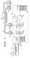
- FIG. 1is a flow diagram of an integrated circuit manufacturing apparatus
- FIG. 2is a diagram of an ammonium hydroxide dilution tool.
- Integrated circuit manufacturing processesinclude numerous steps in which substances are introduced in a wafer or on its surface, and other steps in which material is removed.
- a photolithographic stepincludes depositing a photoresist on the wafer surface, developing the photoresist and removing the undeveloped portion to form a pattern of geometric shapes for exposing portions of the wafer to further processing steps. When these steps are completed, the remaining photoresist is removed.
- Such photolithographic stepsare examples where all of an originally deposited material is residue which must be removed to prevent the fabrication of a defective device.
- a silicon dioxide layersuch as an interlayer dielectric is deposited or grown on the wafer and a pattern is formed with a photoresist layer. The silicon dioxide is selectively etched in the exposed portions of the photoresist to provide openings for connecting between interconnect layers.
- processing stepsare included to remove unwanted material from the wafer to prevent an integrated circuit defect or failure.
- unwanted materialis designated as residue, and includes unwanted material remaining from previous steps as well as material from the current step, such as particles or other impurities introduced by a non-deposition step such as a cleaning step.
- a solutionincludes at least a homogeneous mixture of fluids which does not settle and whose proportions are not fixed, i.e., can be varied.
- a solutioncan include true solutions, colloidal solutions, suspensions and the like.
- FIG. 1is a diagram showing the flow of a semiconductor wafer through part of an integrated circuit manufacturing system which includes a chemical-mechanical polishing (CMP) tool 10 , a wafer scrubber 20 and a dilution tool 100 .
- CMPchemical-mechanical polishing
- CMP tool 10receives an incoming semiconductor wafer at an input 11 and produces a polished, planarized wafer at an output 12 .
- CMP toolis fully automated such that wafers are handled within CMP tool 10 by means of robot arms or similar devices controlled by a control unit within the tool.
- the incoming waferis received after depositing an interconnect dielectric layer or after a metal such as tungsten has been applied as a blanket layer to plug the interlayer via openings in the dielectric layer.
- a typical slurryincludes alumina particles mixed with de-ionized (DI) water with potassium iodate functioning as the buffer.
- DIde-ionized
- the slurryis applied to a first spinning platen designated as the primary platen.
- the alumina particlesproduce a highly abrasive slurry which is applied at a rate that ensures that a specified amount of material is abraded from the wafer at a determinable rate.
- the above polishing stepleaves a residue of potassium iodate, ferric nitrate, tungsten and alumina particles on the wafer.
- Such materialsare contaminants which can cause defects in the wafer that result in inaccurate geometric patterns being produced, structural defects in an integrated circuit component, or corrosion damage which can lead to an integrated circuit failure.
- alumina particlestheir hardness leaves scratches on the surface of the wafer which can also damage an integrated circuit. Therefore, after the first polishing, the wafer is rinsed with DI water to remove the potassium iodate, ferric nitrate, and some of the loose alumina particles.
- Other alumina particlesremain attached to the wafer because their zeta potential is opposite in polarity to the zeta potential of the wafer surface, which produces an attraction force causing the particles to adhere to the wafer.
- the waferAfter rinsing, the wafer is transported to a secondary rotating platen in CMP 100 to receive a second polishing step to buff the scratches from the wafer surface.
- This stepis similar to the first polishing step except that the slurry particles are comprised of softer silicon dioxide in a solution of NH 4 OH or potassium hydroxide and DI water.
- Potassium hydroxideis used to raise the pH of the slurry so that the zeta potential of the silicon dioxide in the slurry is sufficient to prevent agglomeration.
- the zeta potential of the alumina used for the metal polish stepis altered with the result being less affinity of the alumina particles for the oxide surface to facilitate the removal of the alumina particles.
- the waferAfter buffing, the wafer again is rinsed with DI water and kept wet until further processing. Once a wafer dries, it is nearly impossible to remove the particles without damaging the wafer.
- a batch of wet polished wafersare transported from CMP tool 10 to wafer scrubber 20 .
- the wafersare loaded in a cassette 24 and kept wet with DI water from spray heads 22 .
- a waferis scrubbed by passing between brushes 26 , which are formed from a soft, spongy material such as polyvinyl acetate (PVA) and include small protrusions or stubs (not shown) around the circumference. Brushes 26 rotate as the wafer passes such that the protrusions conform to the wafer to gently rub off particles and other residue without damaging the surface. When hydrated, brushes 26 have a high water content, which provides self-lubrication to maintain contact without damaging the wafer.
- PVApolyvinyl acetate
- a 2% NH 4 OH solutionis formed in dilution tool 100 and controlled by a valve 94 to drip onto brush 26 to scrub a wafer.
- the 2% NH 4 OH solutionhas a pH of approximately 12.0, which further modifies the zeta potential of the remaining alumina particles on the wafer to facilitate their removal with brush 26 .
- Control of the NH 4 OH concentrationis critical, because if the concentration is too low, the zeta potential is insufficiently modified and alumina particles retain their affinity to the wafer. If the concentration is too high, wafer materials such as tungsten plugs erode. In either case, damage to the wafer and device failure is likely.
- a concentration ranging from 1.5-2.5% by weighthas been determined to be adequate for removing alumina particles and other residue without damage to the wafer.
- Other methods besides drippingcould be used to apply NH 4 OH solution to brush 26 .
- sprayingcould be used provided that the evaporation of ammonia (NH 3 ) from the finely divided spray particles is controlled to prevent a reduction in the concentration of the solution and a lowered pH.
- brushes 26After scrubbing a number of wafers, particulate matter and other wafer residue accumulate in brushes 26 , some of which can be re-introduced onto the wafer. Therefore, a second scrubbing step is performed using brushes 28 , which are of similar composition as brushes 26 but are cleaner because much of the residue was previously removed by brushes 26 .
- Valve 95controls the flow rate for dripping 2% NH 4 OH solution onto brushes 28 in a step similar to the step described for brushes 26 . Brushes 26 and 28 are rinsed from time to time with the 2% NH 4 OH to remove accumulated particles.
- the waferis moved to a spin drier comprising an infrared or equivalent heat source 30 , a spray nozzle 31 and a spinner 32 .
- the remaining residueis removed from the wafer by rinsing with DI water applied through nozzle 31 while the wafer spins on spinner 32 .
- nozzle 31is turned off and heat source 30 is switched on to spin dry the wafer.
- the dried waferis loaded in a dry cassette 34 for removal from scrubber 20 .
- NH 4 OHis typically obtained in high concentrations which, owing to its hazardous nature, reduces the number of containers that are transported and handled.
- a standard 30% concentrationis widely available commercially and is typically used.
- Dilution tool 100receives the 30% NH 4 OH from a storage tank 91 and DI water from a storage tank 92 .
- the 30% NH 4 OHis diluted with DI water to produce a solution of NH 4 OH with a 2% concentration which flows through tube 93 to valves 94 - 95 and to scrubber 20 as described above.
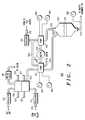
- FIG. 2is a schematic diagram of a dilution and delivery tool 100 including pressure regulators 112 - 114 , a pressure relief valve 116 , a storage ampule 118 , a filter 130 , a conductivity meter 166 , pumps 141 - 142 and a motor 143 .
- Bulk volumes of 30% NH 4 OH solutionare stored in a centralized chemical distribution module (CDM) for delivery to various processing stations in a wafer fabrication facility.
- 30% NH 4 OHis delivered to dilution tool 100 through a tube 151 .
- DI wateris also pumped with a pressure in a range from 10,500-42,200 kilograms per square meter (Kg/M 2 ) gauge through tube 152 .
- Pressure regulator 113reduces the pressure going into ampule 118 and pump 142 to approximately 3,500 Kg/M 2 gauge.
- the 2% NH 4 OH solutionis produced locally near wafer scrubber 20 .
- Ampule 118provides local buffer storage to decouple dilution tool 100 from CDM delivery problems, operating as a local reservoir to ensure a continuous supply of 30% NH 4 OH to dilution tool 100 .
- Sensors 120 - 121are capacitive sensors used to detect the fluid level in ampule 118 . When ampule 118 is full, i.e., at the level of sensors 120 , a signal is sent to the CDM to stop delivering NH 4 OH.
- Continuity in the 30% NH 4 OH supplyis provided by setting sensors 121 to send a delivery command to the CDM before ampule 118 is empty, while an adequate amount of NH 4 OH remains in ampule 118 to operate dilution tool 100 until the CDM has time to replenish the supply.
- sensors 121can be set to send a delivery signal to the CDM when a forty-five minute supply of NH 4 OH remains in ampule 118 .
- sensors 120 and 121are configured in duplicate to provide redundancy as shown. Each of the sensors 120 and 121 communicates with the CDM independently.
- Clean, dry airis pressurized and coupled to ampule 118 through a pressure regulator 113 , which maintains a constant positive pressure in ampule 118 to prevent effervescence and to keep pump 141 primed to avoid pump cavitation.
- the constant pressure within the ampule 118allows decoupling of bulk supply pressure, with its attendant variations in pressure, thus ensuring a stable inlet pressure at the metering pump 141 .
- pressure regulator 113is configured to maintain the pressure within ampule 118 between 3,500 and 5,625 Kg/M 2 gauge.
- dilution tool 100maintains an intermittent flow of 2% NH 4 OH to wafer scrubber 20 even when wafers are not being scrubbed. This flow ensures the purity of the chemicals in that only a miniscule residue volume, and preferably a zero residue volume, of the chemicals is present in the system.
- the presence of an intermittent flowalso has the advantage of continuously cleaning particles from brush 26 .
- ampule 118When ampule 118 is being refilled, the incoming NH 4 OH increases the pressure in ampule 118 above 5,625 Kg/M 2 gauge.
- a pressure relief valve 116is coupled to ampule 118 to bleed off the excess air/NH 3 mixture to maintain the pressure in tube 154 within the specified range of 3,500-5,625 Kg/M 2 gauge.
- Pumps 141 - 142are sealless metering pumps which are commercially available and have numerous advantages when used in semiconductor manufacturing.
- the wetted components of pumps 141 - 142are fabricated with fluoropolymers such as polytetrafluoroethylene (PTFE) and ceramics to allow pumping a wide variety of chemicals without corroding.
- fluoropolymerssuch as polytetrafluoroethylene (PTFE) and ceramics to allow pumping a wide variety of chemicals without corroding.
- PTFEpolytetrafluoroethylene
- citric, oxalic and glacial acetic acidscan be pumped without damage as well as NH 4 OH and potassium hydroxide.
- the pump rotordoes not contact the wall of the pump cavity, which reduces friction and wear and prevents contamination from particles abraded from the pump.
- semiconductor processing chemicalssuch as NH 4 OH can be pumped while maintaining a high level of purity.
- the flow rates through pumps 141 - 142are easily and accurately controlled by an external adjustment that tilts the angle of the rotating piston within the pump cavity (stroke volume).
- the external adjustmentmay be controlled either manually or by a servo control in either an open or closed loop system as is well known in the art.
- pump 141has a small pump head which produces a flow rate of NH 4 OH of four microliters per revolution. Hence, when operating at a low speed of three revolutions per second, the flow rate is twelve microliters per second.
- Dial indicators 162 - 165reveal the amount of tilt in each pump head in order to calibrate flow rates for pumps 141 - 142 , which can be varied manually, mechanically, electronically, etc. Once set, the flow rates remain in a constant ratio even when the overall volume of fluid through pumps 141 - 142 varies. Alternatively, one dial indicator per pump head will indicate pump tilt.
- Pump 142receives DI water through an intake tube 152 at a pressure between 24,600 and 26,725 Kg/M 2 gauge.
- a pressure regulator 114maintains pressure going into pump 142 between 3,500-5,625 Kg/M 2 gauge.
- Pump 142is of similar construction as pump 141 but is substantially larger because fifteen times more water flows through pump 142 to dilute the 30% NH 4 OH solution down to a 2% concentration.
- Motor 143drives pumps 141 - 142 with a single shaft 144 to ensure that pumps 141 - 142 rotate at the same speed and therefore provide NH 4 OH and DI water flow rates at a constant ratio.
- a fixed volume of fluidis pumped through each of the pumps 141 - 142 during each revolution or cycle of motor 143 , so the flow rates can be varied together by adjusting the speed of motor 143 . That is, to produce a larger volume of 2% NH 4 OH solution, the speed of motor 143 is increased accordingly.
- the ratio of the flow rates of 30% NH 4 OH to DI waterremains constant at the higher speed.
- Such speed controlcan be provided by an operator or by using sensors (not shown) coupled to motor 143 through a feedback mechanism (not shown) from wafer scrubber 20 .
- This arrangementallows time-of-use mixing since the pump can generate, in real time, as much or as little 2% NH 4 OH as required to support the cleaning process.
- pumps 141 - 142are sealless, a clearance, e.g., of twenty millionths of a centimeter, is provided between the rotor and pump cavity wall to prevent friction from abrading particles from the pump.
- This clearanceresults in a predetermined portion of chemicals slipping past the pump piston under pressure, which takes the pump out of calibration.
- pumps 141 - 142have approximately one percent pump slip, which means that one percent of the flow is due to input pressure rather than pump action. If the input pressure is too high, the percentage of pump slip increases and results in a deviation from the desired flow rate. Such a deviation can alter the concentration of the solution and result in inadequate or excessive scrubbing of the semiconductor wafer.
- regulators 112 - 114maintain the pressure of fluids going into pumps 141 - 142 within a range from 3,500-5,625 Kg/M 2 gauge.
- a wetting line 154runs from the DI water line to pump 141 to function as a wetting gland of pump 141 .
- a continuous trickle of DI water to wet the rotor of pump 141provides a wet seal to prevent volatile NH 3 from evaporating from the 30% NH 4 OH solution and escaping into the atmosphere as pump 141 rotates.
- Such wettingprevents NH 3 from escaping to create a hazard to the environment or to persons in the vicinity.
- the trickle flowhas the additional advantage of preventing stagnation to ensure the purity of the DI water. Excess DI water is drained from pump 141 through tube 155 .
- Filter 130provides a filtering function as well as a mixing function as described below.
- the filtering functionis achieved with a filter element 131 formed from PTFE which screens out particles larger than 0.2 micrometers in diameter.
- the alumina particles in the CMP slurryare larger than 0.2 micrometers in diameter, so effective cleaning requires a 2% NH 4 OH solution having particles less than 0.2 micrometers in diameter.
- manifold mixingrequires a high rate of flow to agitate the fluids sufficiently to prevent the formation of isolated layers in the manifold.
- the flow ratesare relatively low, such as in dilution tool 100 , there is insufficient agitation present to reliably form a homogeneous solution.
- the 30% NH 4 OH and DI waterhave different densities and flow rates, and are difficult to dissolve homogeneously.
- Dilution tool 100achieves the mixing function at flow rates as low as 0.1 milliliters per second by combining a first fluid (30% NH 4 OH) and a second fluid (DI water) through filter 130 to form the desired 2% NH 4 OH solution to remove residue from a wafer.
- the heaviest fluid or the fluid with the highest flow rateis introduced in filter above the other fluid so as to fall through the other fluid to prevent the fluids from segregating into stratified layers.
- the 30% NH 4 OHis introduced into filter 130 at input port 132 and DI water is introduced at input port 133 , where port 133 is disposed in filter 130 above port 132 .
- port 133is disposed at an elevation approximately three centimeters above that of port 132 .
- filter 130Operation of filter 130 is as follows. Recall that the DI water flows to filter 130 at fifteen times the flow rate of 30% NH 4 OH and that the NH 4 OH is introduced into filter 130 at a lower level. Hence, the larger volume of DI water falls through and turbulates the 30% NH 4 OH, thereby breaking up the NH 4 OH boundary layers or gradients to improve mixing in filter 130 . The turbulence results in more intimate contact between the fluids in filter 130 , which is prolonged and enhanced by the tortuous path through filter element 131 to complete the formation of dilute 2% NH 4 OH solution in filter 130 . The desired 2% NH 4 OH solution flows out of filter 130 through tube 153 to wafer scrubber 20 .
- dilute citric acidis a solution used for removing iron precipitates from the surface of a semiconductor wafer after metal polish.
- prior art systemsuse chemical methods which sample the solution from the bulk storage tank.
- concentrationis determined by removing a sample of solution from the tank and measuring one of its physical or chemical properties, such as specific gravity.
- many waferscan be processed with the solution during the time needed to evaluate the sample, so substantial damage can occur before discovering that the concentration has fallen outside of the specified range.
- a further disadvantage of such systemsis the need to open the system to the atmosphere to take the sample, increasing the risk of contamination and exposing persons in the vicinity to hazardous chemicals.
- prior art systemsare susceptible to samples not being representative of the bulk solutions because of the loss of volatile chemicals at sample taking, sample transport, sample storage, and sample assay, e.g., titration.
- the present inventionuses a conductivity meter 166 disposed in tube 153 to measure the conductivity or resistivity of the solution, which is a function of the concentration of NH 3 .
- Conductivity meter 166remains disposed in tube 153 such that a reading can be taken at any time, or even continuously, to determine conductivity. Such a determination is made in significantly less time than the sample evaluation which characterizes prior art systems. Hence, appropriate steps can be taken to reduce damage to wafers when a defective solution is detected.
- Conductivity meter 166has the further advantage that concentration can be determined without opening the system, which reduces contamination and avoids the risk of exposing nearby persons to hazardous chemicals.
- the conductivity window and the materials of constructionare selected to match the chemical being detected, such as for example, NH 3 , at the concentrations desired in the final mixture.
- the sealless pumpscould be driven by separate motors which can be controlled independently to adjust the solution at the filter output.
- the conductivity metercan measure the conductivity of the solution to provide a control signal to adjust the speed of each motor or the output stroke volume of each pump head to vary the concentration of the solution.
- the motor adjustmentis provided by a feedback path from the conductivity meter to the motors which includes electrical or mechanical devices.
- concentration of the output solutione.g., 2% NH 4 OH
- concentration of the input fluidse.g., 30% NH 4 OH
- Experiment 1Experiment 2
- Experiment 3Manifold Manifold Filter Mixing/ Mixing/Constant Mixing/Intermittent Intermittent Flow Flow Flow Conductivity in ⁇ S Conductivity in ⁇ S 943 1100 1108 972 1121 1107 1065 1087 1108 1069 1087 1122 1072 1096 1122 1072 1083 1122 1105 1083 1111 1096 1096 1109 1051 1099 1116 1096 1099 1115 1099 1069 1114 1099 1122 1098 1074 1122 1097 1022 1024 1122 1002 1104 1122
- the measured conductivities of the resulting filter mixed solutionremained essentially constant and exhibited very low fluctuations in the range of less than about 25 ⁇ S. Such low fluctuations indicate that a homogeneous mixture was produced.
- the present inventionprovides a novel dilution tool and a method of manufacturing an integrated circuit that includes preparing a solution of two fluids for removing residue from a semiconductor wafer.
- the fluidsare mixed in a filter to form the desired solution.
- Sealless pumps driven by a common motorpump the fluids while maintaining a constant ratio of flow rates as the flow rate of the solution varies.
- the concentration of the solutionis determined by measuring the conductivity with a conductivity meter.
- the solution's concentrationis monitored and controlled in a closed loop control system by tilting the angle of the rotating piston within the pump cavity.
- a dilute NH 4 OH solutionis formed in the amount needed, at exactly the time the solution is needed, avoiding the need to prepare and store bulk quantities of a solution whose concentration varies with the evaporation of NH 3 gas.
- the tooloperates in a sealed enclosure to reduce safety and environmental hazards and the need to handle caustic chemicals.
Landscapes
- Engineering & Computer Science (AREA)
- Manufacturing & Machinery (AREA)
- Physics & Mathematics (AREA)
- Condensed Matter Physics & Semiconductors (AREA)
- General Physics & Mathematics (AREA)
- Computer Hardware Design (AREA)
- Microelectronics & Electronic Packaging (AREA)
- Power Engineering (AREA)
- Chemical Kinetics & Catalysis (AREA)
- Chemical & Material Sciences (AREA)
- Cleaning Or Drying Semiconductors (AREA)
- Grinding-Machine Dressing And Accessory Apparatuses (AREA)
- Filtration Of Liquid (AREA)
Abstract
Description
| Experiment 1 | Experiment 2 | Experiment 3 |
| Manifold | Manifold | Filter Mixing/ |
| Mixing/Constant | Mixing/Intermittent | Intermittent |
| Flow | Flow | Flow |
| Conductivity in μS | Conductivity in μS | Conductivity in μS |
| 943 | 1100 | 1108 |
| 972 | 1121 | 1107 |
| 1065 | 1087 | 1108 |
| 1069 | 1087 | 1122 |
| 1072 | 1096 | 1122 |
| 1072 | 1083 | 1122 |
| 1105 | 1083 | 1111 |
| 1096 | 1096 | 1109 |
| 1051 | 1099 | 1116 |
| 1096 | 1099 | 1115 |
| 1099 | 1069 | 1114 |
| 1099 | 1122 | 1098 |
| 1074 | 1122 | 1097 |
| 1022 | 1024 | 1122 |
| 1002 | 1104 | 1122 |
Claims (14)
Priority Applications (1)
| Application Number | Priority Date | Filing Date | Title |
|---|---|---|---|
| US09/495,180US6406555B1 (en) | 1997-07-01 | 2000-02-01 | Point of use dilution tool and method |
Applications Claiming Priority (2)
| Application Number | Priority Date | Filing Date | Title |
|---|---|---|---|
| US08/886,741US6070600A (en) | 1997-07-01 | 1997-07-01 | Point of use dilution tool and method |
| US09/495,180US6406555B1 (en) | 1997-07-01 | 2000-02-01 | Point of use dilution tool and method |
Related Parent Applications (1)
| Application Number | Title | Priority Date | Filing Date |
|---|---|---|---|
| US08/886,741Continuation-In-PartUS6070600A (en) | 1997-07-01 | 1997-07-01 | Point of use dilution tool and method |
Publications (1)
| Publication Number | Publication Date |
|---|---|
| US6406555B1true US6406555B1 (en) | 2002-06-18 |
Family
ID=25389667
Family Applications (2)
| Application Number | Title | Priority Date | Filing Date |
|---|---|---|---|
| US08/886,741Expired - Fee RelatedUS6070600A (en) | 1997-07-01 | 1997-07-01 | Point of use dilution tool and method |
| US09/495,180Expired - LifetimeUS6406555B1 (en) | 1997-07-01 | 2000-02-01 | Point of use dilution tool and method |
Family Applications Before (1)
| Application Number | Title | Priority Date | Filing Date |
|---|---|---|---|
| US08/886,741Expired - Fee RelatedUS6070600A (en) | 1997-07-01 | 1997-07-01 | Point of use dilution tool and method |
Country Status (6)
| Country | Link |
|---|---|
| US (2) | US6070600A (en) |
| JP (1) | JPH1119871A (en) |
| KR (1) | KR100597325B1 (en) |
| CN (1) | CN1145204C (en) |
| SG (1) | SG77642A1 (en) |
| TW (1) | TW393677B (en) |
Cited By (4)
| Publication number | Priority date | Publication date | Assignee | Title |
|---|---|---|---|---|
| US20050001508A1 (en)* | 2003-07-01 | 2005-01-06 | Mitsubishi Denki Kabushiki Kaisha | Rotor for rotary electric rotor |
| US20060217896A1 (en)* | 2003-03-28 | 2006-09-28 | Advanced Technology Materials, Inc. | Photometrically modulated delivery of reagents |
| US20060237061A1 (en)* | 2003-03-28 | 2006-10-26 | Arno Jose I | In-situ gas blending and dilution system for delivery of dilute gas at a predetermined concentration |
| WO2007002288A3 (en)* | 2005-06-22 | 2007-04-05 | Advanced Tech Materials | Apparatus and process for integrated gas blending |
Families Citing this family (9)
| Publication number | Priority date | Publication date | Assignee | Title |
|---|---|---|---|---|
| US6070600A (en)* | 1997-07-01 | 2000-06-06 | Motorola, Inc. | Point of use dilution tool and method |
| US6276997B1 (en)* | 1998-12-23 | 2001-08-21 | Shinhwa Li | Use of chemical mechanical polishing and/or poly-vinyl-acetate scrubbing to restore quality of used semiconductor wafers |
| US6267142B1 (en)* | 1999-06-25 | 2001-07-31 | Lam Research Corporation | Fluid delivery stablization for wafer preparation systems |
| US6405399B1 (en)* | 1999-06-25 | 2002-06-18 | Lam Research Corporation | Method and system of cleaning a wafer after chemical mechanical polishing or plasma processing |
| EP1094506A3 (en) | 1999-10-18 | 2004-03-03 | Applied Materials, Inc. | Capping layer for extreme low dielectric constant films |
| US20030011774A1 (en)* | 2001-06-05 | 2003-01-16 | Dibello Gerald N. | Methods and systems for monitoring process fluids |
| US6589099B2 (en) | 2001-07-09 | 2003-07-08 | Motorola, Inc. | Method for chemical mechanical polishing (CMP) with altering the concentration of oxidizing agent in slurry |
| US7520287B2 (en)* | 2005-01-28 | 2009-04-21 | Kozy David M | Aqueous tube cleaning apparatus and method |
| US20130068264A1 (en)* | 2011-09-21 | 2013-03-21 | Nanya Technology Corporation | Wafer scrubber apparatus |
Citations (12)
| Publication number | Priority date | Publication date | Assignee | Title |
|---|---|---|---|---|
| US3286992A (en)* | 1965-11-29 | 1966-11-22 | Little Inc A | Mixing device |
| US3905395A (en)* | 1972-12-28 | 1975-09-16 | Hewlett Packard Gmbh | Mixing chamber |
| US4159929A (en)* | 1978-05-17 | 1979-07-03 | Hooker Chemicals & Plastics Corp. | Chemical and electro-chemical process for production of alkali metal chlorates |
| US4506987A (en)* | 1982-09-08 | 1985-03-26 | The United States Of America As Represented By The United States Department Of Energy | High pressure liquid chromatographic gradient mixer |
| US4531456A (en)* | 1984-09-26 | 1985-07-30 | Fmc Corporation | Liquid distribution trough |
| US5316384A (en)* | 1992-11-13 | 1994-05-31 | Unosource Controls, Inc. | Primary-secondary circuit hydraulic interface |
| US5439663A (en)* | 1994-08-01 | 1995-08-08 | Fmc Corporation | Method for producing Caro's acid |
| US5779355A (en)* | 1997-02-27 | 1998-07-14 | Roger H. Woods Limited | Mixing apparatus venturi coupled multiple shear mixing apparatus for repairing a liquid-solid slurry |
| US5792354A (en)* | 1994-02-10 | 1998-08-11 | Pharmacia Biotech Ab | Filter well and method for its manufacture |
| US5985045A (en) | 1994-10-24 | 1999-11-16 | Motorola, Inc. | Process for polishing a semiconductor substrate |
| JPH11342323A (en)* | 1998-03-27 | 1999-12-14 | Bayer Ag | Static mixer module |
| US6070600A (en)* | 1997-07-01 | 2000-06-06 | Motorola, Inc. | Point of use dilution tool and method |
Family Cites Families (5)
| Publication number | Priority date | Publication date | Assignee | Title |
|---|---|---|---|---|
| US4911761A (en)* | 1984-05-21 | 1990-03-27 | Cfm Technologies Research Associates | Process and apparatus for drying surfaces |
| JP3341033B2 (en)* | 1993-06-22 | 2002-11-05 | 忠弘 大見 | Rotating chemical solution cleaning method and cleaning device |
| US5407526A (en)* | 1993-06-30 | 1995-04-18 | Intel Corporation | Chemical mechanical polishing slurry delivery and mixing system |
| US5772784A (en)* | 1994-11-14 | 1998-06-30 | Yieldup International | Ultra-low particle semiconductor cleaner |
| US5664990A (en)* | 1996-07-29 | 1997-09-09 | Integrated Process Equipment Corp. | Slurry recycling in CMP apparatus |
- 1997
- 1997-07-01USUS08/886,741patent/US6070600A/ennot_activeExpired - Fee Related
- 1998
- 1998-04-23TWTW087106258Apatent/TW393677B/ennot_activeIP Right Cessation
- 1998-06-25SGSG1998001519Apatent/SG77642A1/enunknown
- 1998-06-30CNCNB981155553Apatent/CN1145204C/ennot_activeExpired - Fee Related
- 1998-06-30JPJP10199832Apatent/JPH1119871A/enactivePending
- 1998-07-01KRKR1019980026343Apatent/KR100597325B1/ennot_activeExpired - Fee Related
- 2000
- 2000-02-01USUS09/495,180patent/US6406555B1/ennot_activeExpired - Lifetime
Patent Citations (12)
| Publication number | Priority date | Publication date | Assignee | Title |
|---|---|---|---|---|
| US3286992A (en)* | 1965-11-29 | 1966-11-22 | Little Inc A | Mixing device |
| US3905395A (en)* | 1972-12-28 | 1975-09-16 | Hewlett Packard Gmbh | Mixing chamber |
| US4159929A (en)* | 1978-05-17 | 1979-07-03 | Hooker Chemicals & Plastics Corp. | Chemical and electro-chemical process for production of alkali metal chlorates |
| US4506987A (en)* | 1982-09-08 | 1985-03-26 | The United States Of America As Represented By The United States Department Of Energy | High pressure liquid chromatographic gradient mixer |
| US4531456A (en)* | 1984-09-26 | 1985-07-30 | Fmc Corporation | Liquid distribution trough |
| US5316384A (en)* | 1992-11-13 | 1994-05-31 | Unosource Controls, Inc. | Primary-secondary circuit hydraulic interface |
| US5792354A (en)* | 1994-02-10 | 1998-08-11 | Pharmacia Biotech Ab | Filter well and method for its manufacture |
| US5439663A (en)* | 1994-08-01 | 1995-08-08 | Fmc Corporation | Method for producing Caro's acid |
| US5985045A (en) | 1994-10-24 | 1999-11-16 | Motorola, Inc. | Process for polishing a semiconductor substrate |
| US5779355A (en)* | 1997-02-27 | 1998-07-14 | Roger H. Woods Limited | Mixing apparatus venturi coupled multiple shear mixing apparatus for repairing a liquid-solid slurry |
| US6070600A (en)* | 1997-07-01 | 2000-06-06 | Motorola, Inc. | Point of use dilution tool and method |
| JPH11342323A (en)* | 1998-03-27 | 1999-12-14 | Bayer Ag | Static mixer module |
Cited By (14)
| Publication number | Priority date | Publication date | Assignee | Title |
|---|---|---|---|---|
| US7925450B2 (en) | 2003-03-28 | 2011-04-12 | Advanced Technology Materials, Inc. | Photometrically modulated delivery of reagents |
| US20060217896A1 (en)* | 2003-03-28 | 2006-09-28 | Advanced Technology Materials, Inc. | Photometrically modulated delivery of reagents |
| US20060237061A1 (en)* | 2003-03-28 | 2006-10-26 | Arno Jose I | In-situ gas blending and dilution system for delivery of dilute gas at a predetermined concentration |
| US7325560B2 (en) | 2003-03-28 | 2008-02-05 | Advanced Technology Materials, Inc. | In-situ gas blending and dilution system for delivery of dilute gas at a predetermined concentration |
| US7373257B2 (en) | 2003-03-28 | 2008-05-13 | Advanced Technology Materials, Inc. | Photometrically modulated delivery of reagents |
| US20080213925A1 (en)* | 2003-03-28 | 2008-09-04 | Advanced Technology Materials, Inc. | Photometrically modulated delivery of reagents |
| US7711496B2 (en) | 2003-03-28 | 2010-05-04 | Advanced Technology Materials, Inc. | Photometrically modulated delivery of reagents |
| US20100217415A1 (en)* | 2003-03-28 | 2010-08-26 | Advanced Technology Materials, Inc. | Photometrically modulated delivery of reagents |
| US8244482B2 (en) | 2003-03-28 | 2012-08-14 | Advanced Technology Materials, Inc. | Photometrically modulated delivery of reagents |
| US20050001508A1 (en)* | 2003-07-01 | 2005-01-06 | Mitsubishi Denki Kabushiki Kaisha | Rotor for rotary electric rotor |
| WO2007002288A3 (en)* | 2005-06-22 | 2007-04-05 | Advanced Tech Materials | Apparatus and process for integrated gas blending |
| US20100224264A1 (en)* | 2005-06-22 | 2010-09-09 | Advanced Technology Materials, Inc. | Apparatus and process for integrated gas blending |
| TWI402098B (en)* | 2005-06-22 | 2013-07-21 | Advanced Tech Materials | Apparatus and process for integrated gas blending |
| US9666435B2 (en) | 2005-06-22 | 2017-05-30 | Entegris, Inc. | Apparatus and process for integrated gas blending |
Also Published As
| Publication number | Publication date |
|---|---|
| CN1208950A (en) | 1999-02-24 |
| US6070600A (en) | 2000-06-06 |
| TW393677B (en) | 2000-06-11 |
| KR100597325B1 (en) | 2006-09-28 |
| CN1145204C (en) | 2004-04-07 |
| JPH1119871A (en) | 1999-01-26 |
| KR19990013494A (en) | 1999-02-25 |
| SG77642A1 (en) | 2001-01-16 |
Similar Documents
| Publication | Publication Date | Title |
|---|---|---|
| US6406555B1 (en) | Point of use dilution tool and method | |
| US6554467B2 (en) | Process and apparatus for blending and distributing a slurry solution | |
| US7118445B2 (en) | Semiconductor workpiece processing methods, a method of preparing semiconductor workpiece process fluid, and a method of delivering semiconductor workpiece process fluid to a semiconductor processor | |
| US6910943B2 (en) | Planarization apparatus and method | |
| US7344298B2 (en) | Method and apparatus for blending process materials | |
| EP0822033A1 (en) | Slurry recycling in chemical-mechanical polishing (CMP) apparatus | |
| US6048256A (en) | Apparatus and method for continuous delivery and conditioning of a polishing slurry | |
| US6338671B1 (en) | Apparatus for supplying polishing liquid | |
| US7743783B2 (en) | Method and apparatus for recycling process fluids | |
| US6357458B2 (en) | Cleaning apparatus and cleaning method | |
| US6039055A (en) | Wafer cleaning with dissolved gas concentration control | |
| US20020142617A1 (en) | Method for evaluating a wafer cleaning operation | |
| JP2006222467A (en) | Planarization processing apparatus | |
| US6130163A (en) | Stabilization of slurry used in chemical mechanical polishing of semiconductor wafers by adjustment of PH of deionized water | |
| JPH0737851A (en) | Cleaning equipment | |
| US20250303329A1 (en) | Filter with metal-organic framework for cmp processing | |
| Singh et al. | A symposium | |
| EP0849778A2 (en) | Improvements in or relating to wafer polishing | |
| CN115155410A (en) | A polishing liquid storage and mixing device | |
| JP2986515B2 (en) | Polishing method and polishing apparatus used therefor |
Legal Events
| Date | Code | Title | Description |
|---|---|---|---|
| AS | Assignment | Owner name:MOTOROLA, INC., ILLINOIS Free format text:ASSIGNMENT OF ASSIGNORS INTEREST;ASSIGNORS:GROOTEGOED, JAMES A.;VANELL, JAMES F.;REEL/FRAME:011073/0958 Effective date:20000516 | |
| STCF | Information on status: patent grant | Free format text:PATENTED CASE | |
| AS | Assignment | Owner name:FREESCALE SEMICONDUCTOR, INC., TEXAS Free format text:ASSIGNMENT OF ASSIGNORS INTEREST;ASSIGNOR:MOTOROLA, INC.;REEL/FRAME:015698/0657 Effective date:20040404 Owner name:FREESCALE SEMICONDUCTOR, INC.,TEXAS Free format text:ASSIGNMENT OF ASSIGNORS INTEREST;ASSIGNOR:MOTOROLA, INC.;REEL/FRAME:015698/0657 Effective date:20040404 | |
| FPAY | Fee payment | Year of fee payment:4 | |
| AS | Assignment | Owner name:CITIBANK, N.A. AS COLLATERAL AGENT, NEW YORK Free format text:SECURITY AGREEMENT;ASSIGNORS:FREESCALE SEMICONDUCTOR, INC.;FREESCALE ACQUISITION CORPORATION;FREESCALE ACQUISITION HOLDINGS CORP.;AND OTHERS;REEL/FRAME:018855/0129 Effective date:20061201 Owner name:CITIBANK, N.A. AS COLLATERAL AGENT,NEW YORK Free format text:SECURITY AGREEMENT;ASSIGNORS:FREESCALE SEMICONDUCTOR, INC.;FREESCALE ACQUISITION CORPORATION;FREESCALE ACQUISITION HOLDINGS CORP.;AND OTHERS;REEL/FRAME:018855/0129 Effective date:20061201 | |
| FPAY | Fee payment | Year of fee payment:8 | |
| AS | Assignment | Owner name:CITIBANK, N.A., AS COLLATERAL AGENT,NEW YORK Free format text:SECURITY AGREEMENT;ASSIGNOR:FREESCALE SEMICONDUCTOR, INC.;REEL/FRAME:024397/0001 Effective date:20100413 Owner name:CITIBANK, N.A., AS COLLATERAL AGENT, NEW YORK Free format text:SECURITY AGREEMENT;ASSIGNOR:FREESCALE SEMICONDUCTOR, INC.;REEL/FRAME:024397/0001 Effective date:20100413 | |
| AS | Assignment | Owner name:CITIBANK, N.A., AS NOTES COLLATERAL AGENT, NEW YORK Free format text:SECURITY AGREEMENT;ASSIGNOR:FREESCALE SEMICONDUCTOR, INC.;REEL/FRAME:030633/0424 Effective date:20130521 Owner name:CITIBANK, N.A., AS NOTES COLLATERAL AGENT, NEW YOR Free format text:SECURITY AGREEMENT;ASSIGNOR:FREESCALE SEMICONDUCTOR, INC.;REEL/FRAME:030633/0424 Effective date:20130521 | |
| AS | Assignment | Owner name:CITIBANK, N.A., AS NOTES COLLATERAL AGENT, NEW YORK Free format text:SECURITY AGREEMENT;ASSIGNOR:FREESCALE SEMICONDUCTOR, INC.;REEL/FRAME:031591/0266 Effective date:20131101 Owner name:CITIBANK, N.A., AS NOTES COLLATERAL AGENT, NEW YOR Free format text:SECURITY AGREEMENT;ASSIGNOR:FREESCALE SEMICONDUCTOR, INC.;REEL/FRAME:031591/0266 Effective date:20131101 | |
| FPAY | Fee payment | Year of fee payment:12 | |
| AS | Assignment | Owner name:FREESCALE SEMICONDUCTOR, INC., TEXAS Free format text:PATENT RELEASE;ASSIGNOR:CITIBANK, N.A., AS COLLATERAL AGENT;REEL/FRAME:037354/0225 Effective date:20151207 Owner name:FREESCALE SEMICONDUCTOR, INC., TEXAS Free format text:PATENT RELEASE;ASSIGNOR:CITIBANK, N.A., AS COLLATERAL AGENT;REEL/FRAME:037356/0553 Effective date:20151207 Owner name:FREESCALE SEMICONDUCTOR, INC., TEXAS Free format text:PATENT RELEASE;ASSIGNOR:CITIBANK, N.A., AS COLLATERAL AGENT;REEL/FRAME:037356/0143 Effective date:20151207 | |
| AS | Assignment | Owner name:MORGAN STANLEY SENIOR FUNDING, INC., MARYLAND Free format text:ASSIGNMENT AND ASSUMPTION OF SECURITY INTEREST IN PATENTS;ASSIGNOR:CITIBANK, N.A.;REEL/FRAME:037486/0517 Effective date:20151207 | |
| AS | Assignment | Owner name:MORGAN STANLEY SENIOR FUNDING, INC., MARYLAND Free format text:ASSIGNMENT AND ASSUMPTION OF SECURITY INTEREST IN PATENTS;ASSIGNOR:CITIBANK, N.A.;REEL/FRAME:037518/0292 Effective date:20151207 | |
| AS | Assignment | Owner name:MORGAN STANLEY SENIOR FUNDING, INC., MARYLAND Free format text:SUPPLEMENT TO THE SECURITY AGREEMENT;ASSIGNOR:FREESCALE SEMICONDUCTOR, INC.;REEL/FRAME:039138/0001 Effective date:20160525 | |
| AS | Assignment | Owner name:NXP, B.V., F/K/A FREESCALE SEMICONDUCTOR, INC., NETHERLANDS Free format text:RELEASE BY SECURED PARTY;ASSIGNOR:MORGAN STANLEY SENIOR FUNDING, INC.;REEL/FRAME:040925/0001 Effective date:20160912 Owner name:NXP, B.V., F/K/A FREESCALE SEMICONDUCTOR, INC., NE Free format text:RELEASE BY SECURED PARTY;ASSIGNOR:MORGAN STANLEY SENIOR FUNDING, INC.;REEL/FRAME:040925/0001 Effective date:20160912 | |
| AS | Assignment | Owner name:NXP B.V., NETHERLANDS Free format text:RELEASE BY SECURED PARTY;ASSIGNOR:MORGAN STANLEY SENIOR FUNDING, INC.;REEL/FRAME:040928/0001 Effective date:20160622 | |
| AS | Assignment | Owner name:NXP USA, INC., TEXAS Free format text:CHANGE OF NAME;ASSIGNOR:FREESCALE SEMICONDUCTOR, INC.;REEL/FRAME:040652/0241 Effective date:20161107 Owner name:NXP USA, INC., TEXAS Free format text:MERGER;ASSIGNOR:FREESCALE SEMICONDUCTOR, INC.;REEL/FRAME:040652/0241 Effective date:20161107 | |
| AS | Assignment | Owner name:NXP USA, INC., TEXAS Free format text:CORRECTIVE ASSIGNMENT TO CORRECT THE NATURE OF CONVEYANCE PREVIOUSLY RECORDED AT REEL: 040652 FRAME: 0241. ASSIGNOR(S) HEREBY CONFIRMS THE MERGER AND CHANGE OF NAME;ASSIGNOR:FREESCALE SEMICONDUCTOR, INC.;REEL/FRAME:041260/0850 Effective date:20161107 | |
| AS | Assignment | Owner name:MORGAN STANLEY SENIOR FUNDING, INC., MARYLAND Free format text:CORRECTIVE ASSIGNMENT TO CORRECT THE REMOVE PATENTS 8108266 AND 8062324 AND REPLACE THEM WITH 6108266 AND 8060324 PREVIOUSLY RECORDED ON REEL 037518 FRAME 0292. ASSIGNOR(S) HEREBY CONFIRMS THE ASSIGNMENT AND ASSUMPTION OF SECURITY INTEREST IN PATENTS;ASSIGNOR:CITIBANK, N.A.;REEL/FRAME:041703/0536 Effective date:20151207 | |
| AS | Assignment | Owner name:SHENZHEN XINGUODU TECHNOLOGY CO., LTD., CHINA Free format text:CORRECTIVE ASSIGNMENT TO CORRECT THE TO CORRECT THE APPLICATION NO. FROM 13,883,290 TO 13,833,290 PREVIOUSLY RECORDED ON REEL 041703 FRAME 0536. ASSIGNOR(S) HEREBY CONFIRMS THE THE ASSIGNMENT AND ASSUMPTION OF SECURITYINTEREST IN PATENTS.;ASSIGNOR:MORGAN STANLEY SENIOR FUNDING, INC.;REEL/FRAME:048734/0001 Effective date:20190217 | |
| AS | Assignment | Owner name:NXP B.V., NETHERLANDS Free format text:RELEASE BY SECURED PARTY;ASSIGNOR:MORGAN STANLEY SENIOR FUNDING, INC.;REEL/FRAME:050744/0097 Effective date:20190903 | |
| AS | Assignment | Owner name:MORGAN STANLEY SENIOR FUNDING, INC., MARYLAND Free format text:CORRECTIVE ASSIGNMENT TO CORRECT THE REMOVE APPLICATION11759915 AND REPLACE IT WITH APPLICATION 11759935 PREVIOUSLY RECORDED ON REEL 037486 FRAME 0517. ASSIGNOR(S) HEREBY CONFIRMS THE ASSIGNMENT AND ASSUMPTION OF SECURITYINTEREST IN PATENTS;ASSIGNOR:CITIBANK, N.A.;REEL/FRAME:053547/0421 Effective date:20151207 | |
| AS | Assignment | Owner name:NXP B.V., NETHERLANDS Free format text:CORRECTIVE ASSIGNMENT TO CORRECT THE REMOVEAPPLICATION 11759915 AND REPLACE IT WITH APPLICATION11759935 PREVIOUSLY RECORDED ON REEL 040928 FRAME 0001. ASSIGNOR(S) HEREBY CONFIRMS THE RELEASE OF SECURITYINTEREST;ASSIGNOR:MORGAN STANLEY SENIOR FUNDING, INC.;REEL/FRAME:052915/0001 Effective date:20160622 | |
| AS | Assignment | Owner name:NXP, B.V. F/K/A FREESCALE SEMICONDUCTOR, INC., NETHERLANDS Free format text:CORRECTIVE ASSIGNMENT TO CORRECT THE REMOVEAPPLICATION 11759915 AND REPLACE IT WITH APPLICATION11759935 PREVIOUSLY RECORDED ON REEL 040925 FRAME 0001. ASSIGNOR(S) HEREBY CONFIRMS THE RELEASE OF SECURITYINTEREST;ASSIGNOR:MORGAN STANLEY SENIOR FUNDING, INC.;REEL/FRAME:052917/0001 Effective date:20160912 |