US6406316B1 - Electrical connector with multiple housings - Google Patents
Electrical connector with multiple housingsDownload PDFInfo
- Publication number
- US6406316B1 US6406316B1US09/706,484US70648400AUS6406316B1US 6406316 B1US6406316 B1US 6406316B1US 70648400 AUS70648400 AUS 70648400AUS 6406316 B1US6406316 B1US 6406316B1
- Authority
- US
- United States
- Prior art keywords
- contacts
- housing
- frame
- connector
- plug
- Prior art date
- Legal status (The legal status is an assumption and is not a legal conclusion. Google has not performed a legal analysis and makes no representation as to the accuracy of the status listed.)
- Expired - Lifetime
Links
Images


Classifications
- H—ELECTRICITY
- H05—ELECTRIC TECHNIQUES NOT OTHERWISE PROVIDED FOR
- H05K—PRINTED CIRCUITS; CASINGS OR CONSTRUCTIONAL DETAILS OF ELECTRIC APPARATUS; MANUFACTURE OF ASSEMBLAGES OF ELECTRICAL COMPONENTS
- H05K7/00—Constructional details common to different types of electric apparatus
- H05K7/02—Arrangements of circuit components or wiring on supporting structure
- H05K7/10—Plug-in assemblages of components, e.g. IC sockets
- H05K7/1053—Plug-in assemblages of components, e.g. IC sockets having interior leads
- H05K7/1061—Plug-in assemblages of components, e.g. IC sockets having interior leads co-operating by abutting
- H—ELECTRICITY
- H01—ELECTRIC ELEMENTS
- H01R—ELECTRICALLY-CONDUCTIVE CONNECTIONS; STRUCTURAL ASSOCIATIONS OF A PLURALITY OF MUTUALLY-INSULATED ELECTRICAL CONNECTING ELEMENTS; COUPLING DEVICES; CURRENT COLLECTORS
- H01R12/00—Structural associations of a plurality of mutually-insulated electrical connecting elements, specially adapted for printed circuits, e.g. printed circuit boards [PCB], flat or ribbon cables, or like generally planar structures, e.g. terminal strips, terminal blocks; Coupling devices specially adapted for printed circuits, flat or ribbon cables, or like generally planar structures; Terminals specially adapted for contact with, or insertion into, printed circuits, flat or ribbon cables, or like generally planar structures
- H01R12/70—Coupling devices
- H01R12/71—Coupling devices for rigid printing circuits or like structures
- H01R12/712—Coupling devices for rigid printing circuits or like structures co-operating with the surface of the printed circuit or with a coupling device exclusively provided on the surface of the printed circuit
- H01R12/714—Coupling devices for rigid printing circuits or like structures co-operating with the surface of the printed circuit or with a coupling device exclusively provided on the surface of the printed circuit with contacts abutting directly the printed circuit; Button contacts therefore provided on the printed circuit
- H—ELECTRICITY
- H01—ELECTRIC ELEMENTS
- H01R—ELECTRICALLY-CONDUCTIVE CONNECTIONS; STRUCTURAL ASSOCIATIONS OF A PLURALITY OF MUTUALLY-INSULATED ELECTRICAL CONNECTING ELEMENTS; COUPLING DEVICES; CURRENT COLLECTORS
- H01R12/00—Structural associations of a plurality of mutually-insulated electrical connecting elements, specially adapted for printed circuits, e.g. printed circuit boards [PCB], flat or ribbon cables, or like generally planar structures, e.g. terminal strips, terminal blocks; Coupling devices specially adapted for printed circuits, flat or ribbon cables, or like generally planar structures; Terminals specially adapted for contact with, or insertion into, printed circuits, flat or ribbon cables, or like generally planar structures
- H01R12/70—Coupling devices
- H01R12/82—Coupling devices connected with low or zero insertion force
- H01R12/83—Coupling devices connected with low or zero insertion force connected with pivoting of printed circuits or like after insertion
- H—ELECTRICITY
- H01—ELECTRIC ELEMENTS
- H01R—ELECTRICALLY-CONDUCTIVE CONNECTIONS; STRUCTURAL ASSOCIATIONS OF A PLURALITY OF MUTUALLY-INSULATED ELECTRICAL CONNECTING ELEMENTS; COUPLING DEVICES; CURRENT COLLECTORS
- H01R13/00—Details of coupling devices of the kinds covered by groups H01R12/70 or H01R24/00 - H01R33/00
- H01R13/02—Contact members
- H01R13/193—Means for increasing contact pressure at the end of engagement of coupling part, e.g. zero insertion force or no friction
- H—ELECTRICITY
- H05—ELECTRIC TECHNIQUES NOT OTHERWISE PROVIDED FOR
- H05K—PRINTED CIRCUITS; CASINGS OR CONSTRUCTIONAL DETAILS OF ELECTRIC APPARATUS; MANUFACTURE OF ASSEMBLAGES OF ELECTRICAL COMPONENTS
- H05K7/00—Constructional details common to different types of electric apparatus
- H05K7/02—Arrangements of circuit components or wiring on supporting structure
- H05K7/10—Plug-in assemblages of components, e.g. IC sockets
- H05K7/1053—Plug-in assemblages of components, e.g. IC sockets having interior leads
- H05K7/1076—Plug-in assemblages of components, e.g. IC sockets having interior leads co-operating by sliding
- H05K7/1084—Plug-in assemblages of components, e.g. IC sockets having interior leads co-operating by sliding pin grid array package carriers
Definitions
- the present inventionrelates to an electrical connector. More specifically, the present invention relates to an electrical connector which has a plurality of housings.
- Improvements in computer systems and communications equipmentgenerally involve miniaturization and increased operating speeds. Designers must adapt the electrical connectors used in these systems to handle such changes.
- ZIF connectorsuse a mechanism either to spread a contact apart before receiving its mating contact or to provide mechanical advantage to a contact so that it may spread apart and engage its mating contact.
- ZIF connectorscan be complex and costly, particularly when miniaturization is required.
- the smaller actuatorsmay not have sufficient strength to spread a contact apart or to mate the contacts.
- the actuatorsalso may not fit within footprint limitations.
- ZIF connectorsmay not provide sufficient contact wipe to ensure a stable electrical contact.
- Another type of electrical connectoruses contacts with differential heights. Some of the contacts reside at one elevation, while the others reside at a different elevation. The taller contacts mate first, followed by the shorter contacts. As a result, the connector exhibits a lower peak insertion force. The peak insertion force is lower because not all of the connectors mate in parallel (i.e. at the same time).
- CTEcoefficient of thermal expansion
- an electrical connectorcomprising: a frame; and a plurality of modules retained by the frame.
- Each modulehas: a housing; a plurality of contacts in the housing; and a plurality of fusible elements secured to the contacts for mounting the connector to a substrate.
- an electrical connectorcomprising: a frame having a plurality of walls defining a perimeter of the connector and defining at least one opening; and a plurality of modules positioned within the at least one opening.
- Each modulehas: a housing; a plurality of contacts in the housing; and a plurality of fusible elements secured to the contacts for mounting the connector to a substrate.
- a surface mount electrical connectorhaving a housing with contacts therein.
- the improvementcomprises a plurality of modules forming the housing.
- FIG. 1is a perspective view of a first alternative embodiment of the present invention in an unmated condition
- FIG. 2is a perspective view of the first alternative embodiment in a mated, open condition
- FIG. 3is a perspective view of the first alternative embodiment in a mated, closed condition
- FIG. 4is a plan view of one component of the first alternative embodiment of the present invention.
- FIG. 5is a plan view of another component of the first alternative embodiment of the present invention.
- FIG. 6is a side view of the first alternative embodiment in a mated, closed condition
- FIG. 7is a perspective view of a second alternative embodiment of the present invention in an unmated condition
- FIG. 8is a perspective view of a second alternative embodiment of the present invention in a mated, open condition
- FIG. 9is a perspective view of a second alternative embodiment of the present invention in a mated, closed condition
- FIG. 10is a plan view of one component of the second alternative embodiment of the present invention.
- FIG. 11is a plan view of another component of the second alternative embodiment of the present invention.
- FIG. 12is a side view of the second alternative embodiment in a mated, closed condition
- FIG. 13is a graph depicting the insertion forces for mating a conventional connector compared to mating a connector of the present invention.
- FIGS. 1-12display several alternative embodiments of the present invention.
- the present inventionis a board-to-board electrical connector having plug and receptacle portions. Rather than mating the contacts in parallel (i.e. all of the contacts at the same time), the plug and receptacle portions sequentially mate the contacts.
- the present inventionachieves sequential mating of the contact by preferably rotating the plug portion relative to the receptacle portion. Hinge assemblies on the plug and receptacle portions interface to allow rotation and to precisely align the contacts on the plug and receptacle portions.
- the sequential mating of the contacts in the present inventionpreferably exhibits a lower peak mating force that electrical connectors that mate the contacts in parallel.
- FIGS. 1-6display one alternative embodiment of the present invention.
- An electrical connector 100includes a plug portion 101 and a receptacle portion 103 .
- Connector 100preferably interconnects two substrates S such as printed circuit boards (PCBs) as seen in FIG. 6 .
- Plug 101 and receptacle 103are removably engageable as shown in FIGS. 1-3. Once engaged, plug 101 can rotate relative to receptacle 103 from the open position shown in FIG. 2 to the closed position shown in FIG. 3 . Rotation of plug 101 relative to receptacle 103 allows the sequential mating of the contacts. Plug 101 and receptacle 103 will now be individually described in greater detail.
- plug 101has a generally planar insulative housing 105 , preferably manufactured from a plastic, such as liquid crystal polymer (LCP).
- Housing 105has a mounting end 107 that faces substrate S and a mating end 109 that faces receptacle 103 .
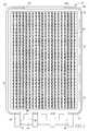
- An array of apertures 147extend through housing 105 from mounting end 107 to mating end 109 .
- An array of contacts 111reside within apertures 147 in housing 105 .
- Apertures 147preferably retain contacts 111 within housing 105 using, for example, a projection 149 extending into aperture 147 from a side wall. Contacts 111 remain within apertures 147 by an interference fit with projection 149 .
- each contact 111generally parallels sides 113 , 115 of housing 105 , and is generally perpendicular to a leading edge 117 and a trailing edge 119 of housing 105 . Since plug 101 and receptacle 103 mate along an axis that is generally parallel to trailing edge 119 , contacts 111 are also generally perpendicular to the mating axis of connector 100 .
- Contacts 111form a series of rows and columns on housing 105 .
- a rowrefers to a group of contacts 111 that extend along the length of housing 105 from leading edge 117 to trailing edge 119 .
- a columnsrefer to a group of contacts 111 that extend along the width of housing 105 between sides 113 , 115 .
- the connectorcould employ several different types of contacts at one time. For example, some contacts could carry a signal or ground, while others carry power. This, for example, allows the connectors of the present invention to be hot matable.
- Housing 105has a wall 121 extending around the perimeter to protects contacts 111 from damage. As seen in FIG. 1, wall 121 could extend around the entire perimeter of housing 105 .
- Leading edge 117 of housing 105includes a tab 123 to assist the user in rotating plug 101 to mate and to unmate with receptacle 103 .
- Trailing edge 119 of housing 105includes a hinge assembly 125 that allows plug 101 to rotate relative to receptacle 103 and to properly align the contacts on plug 101 and receptacle 103 .
- Hinge assembly 125extends generally parallel to the plane of housing 105 . A description of the components of hinge assembly 125 follows.
- a pair of extensions 127project outwardly from trailing edge 119 of housing 105 , each adjacent a respective side 113 , 115 .
- Each extension 127has a curved element 129 flanked by a pair of arms 131 .
- curved elements 129have a first surface 133 shaped to engage a hinge pin on receptacle 103 and a second surface 135 opposite first surface 133 shaped to interact with a block 183 on receptacle 103 .
- Each outermost arm 131has an outwardly facing, or exterior surface 187 , 189 .
- Surfaces 187 , 189interact with corresponding surfaces on the hinge assembly of receptacle 103 to ensure proper alignment of the contacts during mating.
- a centrally located extension 137also projects outwardly from a central location on trailing edge 119 of housing 105 , but extends in a direction opposite of extensions 127 .
- Central extension 137has a curved element 139 flanked by a pair of arms 141 .
- Curved elements 139have a first surface 143 shaped to engage a hinge pin on receptacle 103 and a second surface 145 opposite first surface 133 shaped to interact with a block on receptacle 103 .
- connector 100provides a board-to-board interconnection. Accordingly, plug 101 must mount to substrate S, preferably prior to mating with receptacle 103 .
- Plug 101preferably mounts to substrate S using reflow techniques, in particular Ball Grid Array (BGA) technology.
- BGABall Grid Array
- a fusible element 151such as a solder ball, secures to a tail portion (not shown) of contact 111 .
- International Publication number WO 98/15989International Application number PCT/US97/18066, herein incorporated by reference, describes methods of securing a solder ball to a contact. Fusible element 151 resides, at least partially, within an enlarged portion 153 of aperture 147 .
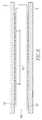
- FIG. 5shows receptacle 103 having a generally planar insulative housing 155 , preferably manufactured from a plastic such as LCP.
- Housing 151has a mounting end 157 facing substrate S and a mating end 159 facing plug 101 .
- An array of apertures 161extend through housing 151 from mounting end 153 to mating end 155 .
- An array of contacts 163reside within apertures 161 in housing 155 .
- Contacts 163can be dual beam contacts and can be retained by the apertures in the same manner as described earlier and as described in International Publication number WO 98/15989.
- each contact 163generally parallels sides 165 , 167 and is generally perpendicular to a leading edge 169 and a trailing edge 171 of housing 155 . Since plug 101 and receptacle 103 mate along an axis that is generally parallel to trailing edge 171 , contacts 163 are also positioned generally perpendicular to the mating axis of connector 100 .
- contacts 163 of receptacle 103form a series of rows and columns on housing 155 . As seen in FIGS. 1 and 2, contacts 163 preferably all have the same elevation. This simplifies the assembly of receptacle 103 .
- each dual beam contact 163preferably have the same length as the other beam. This reduces the amount of material required to form the contact and simplifies the contact forming process.
- Housing 155can have a wall 173 extending around the perimeter to protect contacts 163 from damage. As seen in FIG. 5, wall 173 does not extend around the entire perimeter of housing 155 . Wall 173 has a discontinuity at trailing edge 165 . The discontinuity in wall 173 allows hinge assembly 125 of plug 101 to interact with the hinge assembly of receptacle 103 for complete mating of plug 101 and receptacle 103 .
- Wall 173includes a recessed portion 175 at leading edge 163 of housing 151 .
- Recessed portion 175receives tab 123 on plug 101 when in the mated, closed condition shown in FIGS. 3 and 6.
- Trailing edge 171 of housing 155includes a hinge assembly 177 that allows plug 101 to rotate relative to receptacle 103 .
- Hinge assembly 177extends generally parallel to the plane of housing 155 .
- Hinge assembly 177includes a hinge pin 179 braced by a series of supports 181 along trailing edge 171 of housing 155 .
- a series of blocks 183extend from trailing edge 171 between adjacent supports 181 .
- Blocks 183have curved surfaces 185 that correspond to second surfaces 133 , 143 of extensions 127 and central extension 137 , respectively.
- Curved surfaces 185 of blocks 183have substantially the same shape as second curved surfaces 135 , 145 of extensions 127 and central extension 137 .
- curved surfaces 135 , 145 , 185are circular and have generally the same radius of curvature to ensure proper meshing of hinge assemblies 125 , 177 along the entire mating path. Precise movement of hinge assemblies 125 , 177 ensures proper alignment of contacts 111 , 163 in plug 101 and receptacle 103 during mating.
- Each outermost support 181includes an interior, or inwardly facing surface 195 , 197 of an adjacent block 183 .
- Surfaces 195 , 197interact with surfaces 187 , 189 of hinge assembly 125 to ensure proper alignment of the contacts during mating. Specifically, surfaces 187 , 189 abut surfaces 195 , 197 to laterally align plug 101 relative to receptacle 103 . This helps ensure proper alignment of contacts 111 , 163 during mating.
- connector 100provides a board-to-board interconnection.
- Receptacle 103preferably mounts to substrate S using reflow techniques, in particular BGA technology.
- a fusible elementsuch as a solder ball, secures to a tail portion (not shown) of contact 163 using, for instance, the methods described in the aforementioned International Publication number WO 98/15989.
- the fusible elementresides, at least partially, within an enlarged portion (not shown) of aperture 161 similar to enlarged portion 153 of plug 101 .
- plug 101 and receptacle 103are separate, or unmated, as shown in FIG. 1 .
- hinge assemblies 125 , 177To interface plug 101 and receptacle 103 , hinge assemblies 125 , 177 must mesh as shown in FIG. 2 .
- the features of hinge assemblies 125 , 177 , plug 101 and receptacleenhance the ease of blind mating plug 101 and receptacle 103 .
- extensions 127 and central extension 139enter the openings formed between hinge pin 179 , extensions 181 and trailing edge 171 of housing 155 .
- Arms 131 , 141 of hinge assembly 125enter the areas flanking blocks 183 of hinge assembly 177 .
- Outer surfaces 187 , 189 of arms 131abut inner surfaces 195 , 197 of supports 181 to laterally align plug 101 with receptacle 103 along an axis parallel to trailing edges 119 , 171 .
- curved surfaces 185 of blocks 183begin to abut second surfaces 135 , 145 of extensions 127 and central extension 137 .
- Surfaces 135 , 145 , 185help longitudinally align plug 101 and receptacle 103 along an axis parallel to sides 113 , 115 , 165 , 167 of plug 101 and receptacle 103 .
- the other adjacent surfaces of arm 131 , supports 181 and blocks 185have a clearance therebetween to reduce the amount of force required to rotate plug 101 .
- Extensions 127 and central extension 137provide a retaining force on opposite sides of hinge pin 179 due to the opposite orientation of central extension 137 relative to extensions 127 .
- the retaining forces, along with the placing of extensions 127 and central extension 137 between hinge pin 179 and trailing edge 119 of housing 105prevents separation of plug 101 from receptacle 103 .
- plug 101can only separate from receptacle 103 by reversing the mating process (i.e. rotating plug 101 away from receptacle 103 ).
- the rotation of plug 101begins the mating of contacts 111 , 163 .
- Each contact 111progressively enters into the space between the opposed arms of the dual beam contacts 163 during rotation.
- Each arm of the dual beam contact 163interacts with an opposite surface of blade contact 111 .
- Contact 163retains contact 111 between its resilient dual beams.
- the area between the dual beams of each contact 163is generally parallel to the mating axis of plug 101 and receptacle 103 .
- the column of contacts 111 , 163 closest to trailing edges 119 , 171 of plug 101 and receptacle 103mate first. Mating progresses with each subsequent column away from trailing edges 119 , 171 of plug 101 and receptacle 103 .
- FIGS. 3 and 6shows connector 100 in a fully mated and closed condition. While mated, wall 173 of receptacle 103 can surround wall 121 of plug 101 and tab 123 rests within recess 175 in leading edge 169 of receptacle 103 .
- CTE differentialcan introduce stress into the solder joints that couple the connector and the substrate. Solder joint stress potentially reduces the thermal reliability of the connector.
- CTE differentialcan also warp the connector. Connector warp potentially misaligns the mating connectors, increasing the required peak insertion force. Connector warp may also affect the coplanarity of the fusible elements that couple the connector to the substrate.
- FIGS. 7-12display another alternative embodiment of the present invention. This embodiment helps offset the effects of CTE differential and helps improve coplanarity by using a modular approach.
- the alternative embodimentutilizes several smaller components rather than a unitary, larger component.
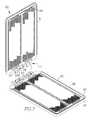
- An electrical connector 200includes a modular plug portion 201 and a modular receptacle portion 203 for interconnecting two substrates S as shown in FIG. 12 .
- Plug 201 and receptacle 203are removably engageable from the unmated condition shown in FIG. 7 to the intermediate, mated, open condition shown in FIG. 8, and ending at the mated, closed condition shown in FIG. 9 .
- Rotation of plug 201 relative to receptacle 203allows the sequential mating of the contacts.
- Plug 201 and receptacle 203will now be described in detail.
- one component of modular plug 201is a frame 205 that supports the remaining components.
- Frame 205is made of a suitable material, including plastic or metal.
- Frame 205can secure to substrate S using, for example, solder or a fastener (not shown).
- Frame 205can provide additional rigidity to substrate S and may serve as a shield, to nearby electrical components, from electromagnetic interference (EMI).
- EMIelectromagnetic interference
- Frame 205has an outer wall 209 defining an opening sized to receive a desired number of removable housings 207 . As seen in FIG. 10, the opening is slightly larger than housing 207 .
- frame 205may include a web 211 that extends between opposed sides of frame 205 . Webs 211 add rigidity to frame 205 and also help retain housing 207 .
- outer wall 209 and web 211define the openings for housings 207 .
- Wall 209 and web 211have projections 213 extending into the opening. Projections 213 engage side walls of housing 207 and maintain housing 207 away from wall 209 . In other words, projections 213 provide a gap between housing 207 and wall 209 to accommodate any housing size variations and any movement of plug 201 during thermal cycles.
- Wall 209also has tabs 215 extending into the opening.
- housing 207rests on tabs 215 when fully inserted within the opening.
- the combination of housing 207 resting on tabs 215 and projections 213 engaging housing 207ensures the retention of housing 207 within frame 205 .
- Frame 205includes a hinge assembly 217 at a trailing edge 219 to allow rotation of plug 201 relative to receptacle 203 .
- Frame 205can be made from metal when, for example, conditions require additional strength from connector 200 or connector 200 will be subjected to numerous mating cycles.
- Hinge assembly 217includes extensions 221 projecting from trailing edge 219 of housing 105 .
- Each extension 221has a curved element 223 flanked by a pair of arms 225 .
- Curved elements 223have a first surface 227 shaped to engage a hinge pin on receptacle 203 and a second surface 229 opposite first curved surface 227 shaped to engage a block 277 on receptacle 203 .
- Each outermost arm 225includes an outwardly facing, or exterior surface 283 , 285 .
- Surfaces 283 , 285interact with corresponding surfaces on the hinge assembly of receptacle 203 to ensure proper alignment of the contacts during mating.
- a centrally located extension 231also projects outwardly from a central location on trailing edge 219 of frame 205 , but extends in a direction opposite of extensions 221 .
- Central extension 231has a curved element 233 flanked by a pair of arms 235 .
- Curved elements 233have a first surface 237 shaped to engage a hinge pin on receptacle 203 and a second surface 239 opposite first curved surface 237 shaped to interact with block 277 on receptacle 203 .
- Plug 201includes a wall 241 projecting from a mating end 243 that faces receptacle 203 .
- Wall 241at least partially extends around the perimeter of frame 205 . As seen in FIG. 10, wall 241 does not reside along trailing edge 219 so as not to interfere with hinge assembly 217 . Wall 241 can protect contacts 247 on housing 207 from damage.
- frame 205can include solder pads 291 .
- Solder pads 291elevate the remainder of frame 205 from substrate S.
- Solder pads 291may help transfer heat to the solder balls on housing 207 during the reflow process and may aid in any visual inspection of the solder balls after securing plug 201 to substrate S.
- solder pads 291can aid in any cleaning that must be done between frame 205 and substrate S after securing to substrate S.
- Frame 205can also secure to substrate S in other manners.
- frame 205could have apertures (not shown) therethrough to receive a fastener (not shown), such as a screw, securable to substrate S.
- housing 207is generally planar and preferably manufactured from a suitable plastic, such as liquid crystal polymer (LCP). Housings 207 seat within the opening in frame 205 .
- LCPliquid crystal polymer
- An array of apertures 245extend through housing 207 .
- Contacts 247reside within apertures 245 , preferably by interference fit.
- FIG. 10displays contacts 247 as blade-type contacts, however other types of contacts, including round pins, could be used.
- Contacts 247form a series of rows and columns on housing 205 . Each contact 247 generally parallels a side 249 of plug 201 and is generally perpendicular to a leading edge 251 of plug 201 .
- aperture 245has an enlarged opening 255 to receive at least a portion of a fusible element 257 , such as a solder ball. Fusible element 257 secures to a tail end of contact 247 .
- a fusible element 257such as a solder ball.
- Fusible element 257secures to a tail end of contact 247 .
- International Publication number WO 98/15989International Application number PCT/US97/18066 describes methods of securing a solder ball to a contact.
- Housing 207can have notches 259 along its outer wall. Some notches 259 are sized to correspond to projections 213 of frame 205 , while other notches 259 are sized to correspond to tabs 215 of frame 205 . Notches 259 help align housing 207 within the opening in frame 205 .
- receptacle 203is identical to plug 201 .
- the followingprovides only a brief summary of the features of receptacle 203 that are similar to features in plug 201 and a more detailed description of the features that differ from plug 201 .
- Modular receptacle 203uses a frame 261 that receives at least one removable housing 263 .
- Frame 261has a wall 265 bordering a portion of the perimeter. Wall 265 can help protect the contacts of housing 263 .
- frame 261has a channel 267 located inwardly from wall 265 .
- Frame 261includes a hinge assembly 269 similar to the hinge assembly in the first alternative embodiment of the present invention.
- Hinge assembly 269includes a hinge pin 271 braced by a series of supports 273 along a trailing edge 275 of frame 261 .
- a series of blocks 277extend from trailing edge 275 of frame 261 between adjacent supports 273 .
- Blocks 277have curved surfaces 279 that correspond to second curved surfaces 229 , 239 of extensions 221 , 231 , respectively.
- Curved surfaces 279 of blocks 277have substantially the same shape as second curved surfaces 229 , 239 of extensions 221 , 231 .
- curved surfaces 229 , 239 , 279are circular and have generally the same radius of curvature to ensure proper meshing of hinge assemblies 217 , 269 along the entire mating path. Precise movement of hinge assemblies 217 , 269 ensures proper alignment of contacts 247 , 281 in plug 201 and receptacle 203 during mating.
- Each outermost support 273includes an interior, or inwardly facing surface 291 , 293 .
- Surfaces 291 , 293interact with surfaces 283 , 285 of hinge assembly 217 to ensure proper alignment of the contacts during mating.
- outer surfaces 283 , 285abut surfaces 291 , 293 to laterally align plug 201 relative to receptacle 203 . This helps ensure proper alignment of contacts 247 , 281 during mating.
- the mating of plug 201 and receptacle 203proceeds as shown in FIGS. 7-9 in the manner described above with respect to the first embodiment.
- Housing 263save the type of contact, is identical to housing 207 of plug 201 .
- FIG. 11demonstrates housing 263 using a dual beam-type contact 281 to mate with blade-type contact 247 of plug 201 .
- contact 281can be any suitable type of contact.
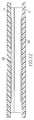
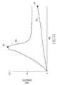
- FIG. 13compares the estimated insertion forces for a typical connector and a connector of the present invention.
- a typical connectorrefers to a connector in which all of the contacts mate in parallel. In other words, a typical contact mates all of the contacts at the same time.
- a typical connectorproduces the insertion force-versus-time path designated 901 in FIG. 13.
- a typical connectorexhibits a peak at the point designated 903 along path 901 . The peak is located approximately midstream along the time period.
- a connector of the present invention(using the same number of contacts, but sequentially mated) produces the insertion force-versus-time path designated 905 in FIG. 13 .
- the connector of the present inventionexhibits a peak at the point designated 907 along path 905 .
- the peakis located approximately at the end of the time period.
- the peak insertion force 907 of a connector of the present inventionis well below the peak insertion force 903 of a typical connector.
Landscapes
- Engineering & Computer Science (AREA)
- Microelectronics & Electronic Packaging (AREA)
- Coupling Device And Connection With Printed Circuit (AREA)
- Details Of Connecting Devices For Male And Female Coupling (AREA)
Abstract
Description
Claims (8)
Priority Applications (1)
| Application Number | Priority Date | Filing Date | Title |
|---|---|---|---|
| US09/706,484US6406316B1 (en) | 1998-01-31 | 2000-11-03 | Electrical connector with multiple housings |
Applications Claiming Priority (4)
| Application Number | Priority Date | Filing Date | Title |
|---|---|---|---|
| US7328198P | 1998-01-31 | 1998-01-31 | |
| US09/209,132US6093042A (en) | 1998-12-10 | 1998-12-10 | High density connector with low insertion force |
| US09/216,574US6155860A (en) | 1998-01-31 | 1998-12-18 | Socket for electrical component |
| US09/706,484US6406316B1 (en) | 1998-01-31 | 2000-11-03 | Electrical connector with multiple housings |
Related Parent Applications (1)
| Application Number | Title | Priority Date | Filing Date |
|---|---|---|---|
| US09/216,574ContinuationUS6155860A (en) | 1998-01-31 | 1998-12-18 | Socket for electrical component |
Publications (1)
| Publication Number | Publication Date |
|---|---|
| US6406316B1true US6406316B1 (en) | 2002-06-18 |
Family
ID=27372262
Family Applications (1)
| Application Number | Title | Priority Date | Filing Date |
|---|---|---|---|
| US09/706,484Expired - LifetimeUS6406316B1 (en) | 1998-01-31 | 2000-11-03 | Electrical connector with multiple housings |
Country Status (1)
| Country | Link |
|---|---|
| US (1) | US6406316B1 (en) |
Cited By (2)
| Publication number | Priority date | Publication date | Assignee | Title |
|---|---|---|---|---|
| US20040266249A1 (en)* | 2003-06-30 | 2004-12-30 | Dobbs Robert William | Pivot component coupled with first circuit board for control of relative alignment of first circuit board connection component with second circuit board connection component |
| EP3297100A3 (en)* | 2016-08-25 | 2018-06-13 | ITT Manufacturing Enterprises LLC | Low profile sealing interconnect with latching interface |
Citations (41)
| Publication number | Priority date | Publication date | Assignee | Title |
|---|---|---|---|---|
| US2779011A (en) | 1954-02-01 | 1957-01-22 | Edison Swan Electric Co Ltd | Manufacture of electrical socket contacts |
| US3133775A (en) | 1962-06-04 | 1964-05-19 | Amp Inc | Multiple contact assembly |
| US3409857A (en) | 1965-08-23 | 1968-11-05 | Amp Inc | Electrical connectors for terminating leads of micro-modular components or the like |
| US3771109A (en) | 1972-05-01 | 1973-11-06 | Bunker Ramo | Electrical connector for integrated circuit device |
| US3865462A (en) | 1973-03-07 | 1975-02-11 | Amp Inc | Preloaded contact and latchable housing assembly |
| US4175821A (en) | 1978-05-15 | 1979-11-27 | Teradyne, Inc. | Electrical connector |
| US4220383A (en) | 1979-04-06 | 1980-09-02 | Amp Incorporated | Surface to surface connector |
| US4257665A (en) | 1978-02-01 | 1981-03-24 | Amp Incorporated | Polarized electrical connector |
| US4341429A (en) | 1980-10-20 | 1982-07-27 | Amp Incorporated | Electrical connector |
| US4354720A (en) | 1980-10-20 | 1982-10-19 | Amp Incorporated | Connector assembly having improved latching means |
| US4368939A (en) | 1980-04-18 | 1983-01-18 | E. I. Du Pont De Nemours And Company | Modular connector housing |
| US4396140A (en) | 1981-01-27 | 1983-08-02 | Bell Telephone Laboratories, Incorporated | Method of bonding electronic components |
| US4504105A (en) | 1982-09-21 | 1985-03-12 | Amp Incorporated | Release mechanism for a connector cover |
| US4503608A (en) | 1983-02-16 | 1985-03-12 | Elfab Corporation | Card edge connector tool and a method of joining a card edge connector |
| US4552422A (en) | 1983-03-14 | 1985-11-12 | Amp Incorporated | Modular receptacle pin grid array |
| US4591230A (en) | 1984-06-29 | 1986-05-27 | Frank Roldan | Electrical connector receptacle |
| NL8500043A (en) | 1985-01-08 | 1986-08-01 | Du Pont Nederland | Multicontact connector strip for printed circuit - can be fitted to other strips for max. packing density |
| US4761140A (en) | 1987-02-20 | 1988-08-02 | Augat Inc. | Minimum insertion force self-cleaning anti-overstress PLCC receiving socket |
| US4836798A (en) | 1987-12-21 | 1989-06-06 | Wells Electronics, Inc. | Zero insertion socket with normally closed contacts |
| US4869681A (en) | 1987-08-28 | 1989-09-26 | Siemens Aktiengesellschaft | Front plug system with lagging end contact arrangement |
| US4887976A (en) | 1988-08-18 | 1989-12-19 | Amp Incorporated | Electrical terminals for flat power cable |
| US4941840A (en) | 1987-12-11 | 1990-07-17 | Universal Co., Ltd. | Circuit board mounting apparatus |
| US5000689A (en) | 1989-01-30 | 1991-03-19 | Japan Aviation Electronics Industry, Ltd. | Connector for integrated circuit packages |
| US5057031A (en) | 1990-08-15 | 1991-10-15 | Aries Electronics, Inc. | Zero insertion force pin grid array test socket |
| US5123855A (en) | 1991-04-26 | 1992-06-23 | Minnesota Mining And Manufacturing Company | Zero insertion force connector for printed circuit boards |
| US5147213A (en) | 1991-10-24 | 1992-09-15 | Minnesota Mining And Manufacturing Company | Zero insertion pressure test socket for pin grid array electronic packages |
| US5215472A (en) | 1991-08-22 | 1993-06-01 | Augat Inc. | High density grid array socket |
| US5268820A (en) | 1992-08-18 | 1993-12-07 | Mitac International Corp. | Mother board assembly |
| US5302136A (en) | 1992-11-23 | 1994-04-12 | Modicon, Inc. | Apparatus for positively preventing misengagement of multipoint connector elements |
| US5378169A (en) | 1993-09-24 | 1995-01-03 | The Whitaker Corporation | Pivotal connector for planar electronic devices |
| US5399108A (en) | 1993-09-08 | 1995-03-21 | Tongrand Limited | LIF PGA socket and contact therein and method making the same |
| US5531605A (en) | 1993-01-06 | 1996-07-02 | Sumitomo Wiring Systems, Ltd. | Lever type connector |
| US5602719A (en) | 1995-11-13 | 1997-02-11 | Intel Corporation | No handle zip socket |
| US5649836A (en) | 1994-10-18 | 1997-07-22 | Japan Aviation Electronics Industry, Limited | Electrical connector having a menber preloading a contact to reduce an insertion force |
| US5762511A (en) | 1994-10-11 | 1998-06-09 | Methode Eletronics, Inc. | Zero insertion force pin grid array socket |
| US5876219A (en) | 1997-08-29 | 1999-03-02 | The Whitaker Corp. | Board-to-board connector assembly |
| US5966023A (en) | 1996-09-16 | 1999-10-12 | Virginia Panel Corporation | Rapid action engagement interface connection system |
| US6004142A (en) | 1997-03-04 | 1999-12-21 | Micron Technology, Inc. | Interposer converter to allow single-sided contact to circuit modules |
| WO2000031829A2 (en) | 1998-11-24 | 2000-06-02 | Teradyne, Inc. | Electrical connector |
| WO2000031832A1 (en) | 1998-11-24 | 2000-06-02 | Teradyne, Inc. | High density electrical connector |
| WO2000031833A1 (en) | 1998-11-24 | 2000-06-02 | Teradyne, Inc. | Electrical connector |
- 2000
- 2000-11-03USUS09/706,484patent/US6406316B1/ennot_activeExpired - Lifetime
Patent Citations (42)
| Publication number | Priority date | Publication date | Assignee | Title |
|---|---|---|---|---|
| US2779011A (en) | 1954-02-01 | 1957-01-22 | Edison Swan Electric Co Ltd | Manufacture of electrical socket contacts |
| US3133775A (en) | 1962-06-04 | 1964-05-19 | Amp Inc | Multiple contact assembly |
| US3409857A (en) | 1965-08-23 | 1968-11-05 | Amp Inc | Electrical connectors for terminating leads of micro-modular components or the like |
| US3771109A (en) | 1972-05-01 | 1973-11-06 | Bunker Ramo | Electrical connector for integrated circuit device |
| US3865462A (en) | 1973-03-07 | 1975-02-11 | Amp Inc | Preloaded contact and latchable housing assembly |
| US4257665A (en) | 1978-02-01 | 1981-03-24 | Amp Incorporated | Polarized electrical connector |
| US4175821A (en) | 1978-05-15 | 1979-11-27 | Teradyne, Inc. | Electrical connector |
| US4220383A (en) | 1979-04-06 | 1980-09-02 | Amp Incorporated | Surface to surface connector |
| US4368939A (en) | 1980-04-18 | 1983-01-18 | E. I. Du Pont De Nemours And Company | Modular connector housing |
| US4354720A (en) | 1980-10-20 | 1982-10-19 | Amp Incorporated | Connector assembly having improved latching means |
| US4341429A (en) | 1980-10-20 | 1982-07-27 | Amp Incorporated | Electrical connector |
| US4396140A (en) | 1981-01-27 | 1983-08-02 | Bell Telephone Laboratories, Incorporated | Method of bonding electronic components |
| US4504105A (en) | 1982-09-21 | 1985-03-12 | Amp Incorporated | Release mechanism for a connector cover |
| US4503608A (en) | 1983-02-16 | 1985-03-12 | Elfab Corporation | Card edge connector tool and a method of joining a card edge connector |
| US4552422A (en) | 1983-03-14 | 1985-11-12 | Amp Incorporated | Modular receptacle pin grid array |
| US4591230A (en) | 1984-06-29 | 1986-05-27 | Frank Roldan | Electrical connector receptacle |
| NL8500043A (en) | 1985-01-08 | 1986-08-01 | Du Pont Nederland | Multicontact connector strip for printed circuit - can be fitted to other strips for max. packing density |
| US4761140A (en) | 1987-02-20 | 1988-08-02 | Augat Inc. | Minimum insertion force self-cleaning anti-overstress PLCC receiving socket |
| US4869681A (en) | 1987-08-28 | 1989-09-26 | Siemens Aktiengesellschaft | Front plug system with lagging end contact arrangement |
| US4941840A (en) | 1987-12-11 | 1990-07-17 | Universal Co., Ltd. | Circuit board mounting apparatus |
| US4836798A (en) | 1987-12-21 | 1989-06-06 | Wells Electronics, Inc. | Zero insertion socket with normally closed contacts |
| US4887976A (en) | 1988-08-18 | 1989-12-19 | Amp Incorporated | Electrical terminals for flat power cable |
| US5000689A (en) | 1989-01-30 | 1991-03-19 | Japan Aviation Electronics Industry, Ltd. | Connector for integrated circuit packages |
| US5057031A (en) | 1990-08-15 | 1991-10-15 | Aries Electronics, Inc. | Zero insertion force pin grid array test socket |
| US5123855A (en) | 1991-04-26 | 1992-06-23 | Minnesota Mining And Manufacturing Company | Zero insertion force connector for printed circuit boards |
| US5215472A (en) | 1991-08-22 | 1993-06-01 | Augat Inc. | High density grid array socket |
| US5147213A (en) | 1991-10-24 | 1992-09-15 | Minnesota Mining And Manufacturing Company | Zero insertion pressure test socket for pin grid array electronic packages |
| US5268820A (en) | 1992-08-18 | 1993-12-07 | Mitac International Corp. | Mother board assembly |
| US5302136A (en) | 1992-11-23 | 1994-04-12 | Modicon, Inc. | Apparatus for positively preventing misengagement of multipoint connector elements |
| US5531605A (en) | 1993-01-06 | 1996-07-02 | Sumitomo Wiring Systems, Ltd. | Lever type connector |
| US5399108A (en) | 1993-09-08 | 1995-03-21 | Tongrand Limited | LIF PGA socket and contact therein and method making the same |
| US5378169A (en) | 1993-09-24 | 1995-01-03 | The Whitaker Corporation | Pivotal connector for planar electronic devices |
| US5762511A (en) | 1994-10-11 | 1998-06-09 | Methode Eletronics, Inc. | Zero insertion force pin grid array socket |
| US5649836A (en) | 1994-10-18 | 1997-07-22 | Japan Aviation Electronics Industry, Limited | Electrical connector having a menber preloading a contact to reduce an insertion force |
| US5602719A (en) | 1995-11-13 | 1997-02-11 | Intel Corporation | No handle zip socket |
| US5966023A (en) | 1996-09-16 | 1999-10-12 | Virginia Panel Corporation | Rapid action engagement interface connection system |
| US6004142A (en) | 1997-03-04 | 1999-12-21 | Micron Technology, Inc. | Interposer converter to allow single-sided contact to circuit modules |
| US5876219A (en) | 1997-08-29 | 1999-03-02 | The Whitaker Corp. | Board-to-board connector assembly |
| WO2000031829A2 (en) | 1998-11-24 | 2000-06-02 | Teradyne, Inc. | Electrical connector |
| WO2000031832A1 (en) | 1998-11-24 | 2000-06-02 | Teradyne, Inc. | High density electrical connector |
| WO2000031833A1 (en) | 1998-11-24 | 2000-06-02 | Teradyne, Inc. | Electrical connector |
| US6152747A (en) | 1998-11-24 | 2000-11-28 | Teradyne, Inc. | Electrical connector |
Cited By (4)
| Publication number | Priority date | Publication date | Assignee | Title |
|---|---|---|---|---|
| US20040266249A1 (en)* | 2003-06-30 | 2004-12-30 | Dobbs Robert William | Pivot component coupled with first circuit board for control of relative alignment of first circuit board connection component with second circuit board connection component |
| US6896539B2 (en)* | 2003-06-30 | 2005-05-24 | Hewlett-Packard Development Company, L.P. | Pivot component coupled with first circuit board for control of relative alignment of first circuit board connection component with second circuit board connection component |
| EP3297100A3 (en)* | 2016-08-25 | 2018-06-13 | ITT Manufacturing Enterprises LLC | Low profile sealing interconnect with latching interface |
| US10476204B2 (en) | 2016-08-25 | 2019-11-12 | Itt Manufacturing Enterprises Llc | Low profile sealing interconnect with latching interface |
Similar Documents
| Publication | Publication Date | Title |
|---|---|---|
| US6482050B1 (en) | Contact for electrical component socket | |
| EP0510995B1 (en) | Electrical connector having reliable terminals | |
| US5320541A (en) | Electrical connector having terminals which cooperate with the edge of a circuit board | |
| EP0416322B1 (en) | Contact terminal in a circuit panel socket | |
| US5545051A (en) | Board to board matable assembly | |
| CN100372180C (en) | Improved socket | |
| US5582519A (en) | Make-first-break-last ground connections | |
| KR0141902B1 (en) | Electrical Connectors for Edge Mount Circuit Boards | |
| EP0543278B1 (en) | Low profile electrical connector | |
| EP1049202B1 (en) | Electrical connector | |
| EP0801821A1 (en) | Electrical connector | |
| EP1128477A2 (en) | Electrical connector with compression contacts | |
| US6350141B1 (en) | Connector frame for a high density electrical connector | |
| US6132258A (en) | Board to board electrical connector | |
| US6093042A (en) | High density connector with low insertion force | |
| KR0138832B1 (en) | Edge mounted circuit board electrical connector | |
| JP3325050B2 (en) | Connector assembly | |
| US6406316B1 (en) | Electrical connector with multiple housings | |
| EP0299989B1 (en) | High density circuit panel socket | |
| US20020115318A1 (en) | Electrical connector and circuit with center ground plane | |
| EP0510869B1 (en) | Electrical connector having terminals which cooperate with the edge of a circuit board | |
| US20020048986A1 (en) | Electrical connector with discrete sections | |
| JPH05299143A (en) | Electric connector | |
| GB2271221A (en) | Mounting an electrical connector on a PCB | |
| CA2571599A1 (en) | Contact for electrical component socket |
Legal Events
| Date | Code | Title | Description |
|---|---|---|---|
| STCF | Information on status: patent grant | Free format text:PATENTED CASE | |
| FPAY | Fee payment | Year of fee payment:4 | |
| AS | Assignment | Owner name:FCI AMERICAS TECHNOLOGY, INC., NEVADA Free format text:CHANGE OF NAME;ASSIGNOR:BERG TECHNOLOGY, INC.;REEL/FRAME:017537/0384 Effective date:20000808 | |
| AS | Assignment | Owner name:BANC OF AMERICA SECURITIES LIMITED, AS SECURITY AG Free format text:SECURITY AGREEMENT;ASSIGNOR:FCI AMERICAS TECHNOLOGY, INC.;REEL/FRAME:017400/0192 Effective date:20060331 | |
| FPAY | Fee payment | Year of fee payment:8 | |
| AS | Assignment | Owner name:FCI AMERICAS TECHNOLOGY, INC., NEVADA Free format text:CHANGE OF NAME;ASSIGNOR:BERG TECHNOLOGY, INC.;REEL/FRAME:026064/0565 Effective date:19990611 Owner name:FCI AMERICAS TECHNOLOGY LLC, NEVADA Free format text:CONVERSION TO LLC;ASSIGNOR:FCI AMERICAS TECHNOLOGY, INC.;REEL/FRAME:026064/0573 Effective date:20090930 | |
| AS | Assignment | Owner name:FCI AMERICAS TECHNOLOGY LLC (F/K/A FCI AMERICAS TE Free format text:RELEASE OF PATENT SECURITY INTEREST AT REEL/FRAME NO. 17400/0192;ASSIGNOR:BANC OF AMERICA SECURITIES LIMITED;REEL/FRAME:029377/0632 Effective date:20121026 | |
| FPAY | Fee payment | Year of fee payment:12 | |
| AS | Assignment | Owner name:WILMINGTON TRUST (LONDON) LIMITED, UNITED KINGDOM Free format text:SECURITY AGREEMENT;ASSIGNOR:FCI AMERICAS TECHNOLOGY LLC;REEL/FRAME:031896/0696 Effective date:20131227 | |
| AS | Assignment | Owner name:FCI AMERICAS TECHNOLOGY LLC, NEVADA Free format text:RELEASE BY SECURED PARTY;ASSIGNOR:WILMINGTON TRUST (LONDON) LIMITED;REEL/FRAME:037484/0169 Effective date:20160108 |