US6405273B1 - Data processing device with memory coupling unit - Google Patents
Data processing device with memory coupling unitDownload PDFInfo
- Publication number
- US6405273B1 US6405273B1US09/192,170US19217098AUS6405273B1US 6405273 B1US6405273 B1US 6405273B1US 19217098 AUS19217098 AUS 19217098AUS 6405273 B1US6405273 B1US 6405273B1
- Authority
- US
- United States
- Prior art keywords
- bus
- memory
- coupling
- sub
- couplers
- Prior art date
- Legal status (The legal status is an assumption and is not a legal conclusion. Google has not performed a legal analysis and makes no representation as to the accuracy of the status listed.)
- Expired - Lifetime
Links
Images


Classifications
- G—PHYSICS
- G06—COMPUTING OR CALCULATING; COUNTING
- G06F—ELECTRIC DIGITAL DATA PROCESSING
- G06F13/00—Interconnection of, or transfer of information or other signals between, memories, input/output devices or central processing units
- G06F13/14—Handling requests for interconnection or transfer
- G06F13/16—Handling requests for interconnection or transfer for access to memory bus
- G06F13/1668—Details of memory controller
- G06F13/1678—Details of memory controller using bus width
Definitions
- the present inventionrelates to a data processing device with a memory coupling unit.
- Data processing devicessuch as microprocessors or microcontrollers comprise one or more register files for intermediate storage of data and addresses.
- the content of these registershas to be loaded and stored into a memory subsystem which can consist of standard memory and/or a cache memory.
- a memory subsystemwhich can consist of standard memory and/or a cache memory.
- an interface between the register file and the memory subsystemis provided which is controlled by respective control units of the microprocessor during load and store cycles.
- Modern microprocessorsprovide superscalar design with the ability of processing multiple instructions in parallel. Furthermore, in digital signal processing some instructions require multiple data which is processed during execution of the respective instruction.
- the interface between the register file and the memorycan be a bottleneck within the processing path and slow down the over all speed of the respective microprocessor.
- a data processing unitwith a register file having a plurality of registers, a memory having a plurality of n-bit input/output ports, and a coupling unit for coupling the memory with the register file, a memory address and select unit for addressing the memory banks.
- the coupling unitcomprises a bus having a bus width of at least 2n-bits forming at least a first and second sub-bus, first couplers for coupling each memory bank or the register file selectively with one of the sub-busses, and second couplers for coupling the register file or the memory banks with the bus.
- the data processing unitcomprises a first and a second register file having a plurality of registers, a memory having a plurality of n-bit input/output ports, a bus having a bus width of at least 2n-bits forming at least a first and second sub-bus, first couplers for coupling each memory bank selectively with one of the sub-busses, second couplers for coupling the first register file with the bus, and third couplers for coupling the second register file with the bus.
- a data processing unitcomprises a first and a second register file having a plurality of registers, a first and second memory each having a plurality of n-bit input/output ports, a first bus having a bus width of at least 2n-bits forming at least a first and second sub-bus, first couplers for coupling each memory bank of said first memory selectively with one of the sub-busses, second couplers for coupling said first register file with said first bus, a second bus having a bus width of at least 2n-bits forming at least a third and fourth sub-bus, third couplers for coupling each memory bank of said second memory selectively with one of the sub-busses, fourth couplers for coupling the second register file with the second bus, and a bus-coupler for coupling the first and second bus.
- FIGS. 1 a and 1 bshow a block diagram of first embodiments including a memory sub-system, a coupling interface and a register file according to the present invention
- FIG. 2shows a block diagram of a second embodiment including a memory sub-system coupled with a register file according to the present invention
- FIG. 3shows a block diagram of a third embodiment with a memory subsystem coupled with a register file according to the present invention
- FIG. 4shows a block diagram of a fourth embodiment with a coupling unit between a memory system and two register files according to the invention
- FIG. 5shows details of the coupling unit coupling multiple banks with a register file
- FIG. 6shows an addressing scheme of a multiple bank memory system
- FIG. 7shows another addressing scheme of a multiple bank memory system
- FIG. 8shows the bus-bridge according to FIG. 4 in more detail
- FIG. 9is a further embodiment showing a memory and a interface of the present invention.
- FIG. 10shows a data transfer of a first type using the embodiment of FIG. 4.
- FIG. 11shows a data transfer of a second type using the embodiment of FIG. 4.
- FIG. 12shows a context switch data transfer using the embodiment of FIG. 4,
- FIG. 13shows a single bus line structure with a bus holder
- FIG. 14shows a different embodiment of a bus holder.
- FIG. 1 ashows an embodiment of simple implementation of the principles according to the present invention.
- a memory sub-systemcontains two memory banks 101 and 102 .
- memory bankmeans a memory block containing either multiple banks or towers organized in one or more data bytes or a single memory organized in multiple bytes.
- the memory sub-systemcan be either cache memory or standard memory.
- the memory banks 101 and 102are addressed and selected by a memory address and select unit 9 .
- Each memory bankoutputs 16 bit data at its respective data input/output port.
- the output portsare coupled with the input of 2 ⁇ 16 multiplexers 401 , 402 , respectively.
- Each multiplexer 401 and 402comprises two 16 bit outputs which are coupled with 16 bit sub-busses 410 and 420 .
- a register file 8is provided which contains a plurality of 16 bit registers 81 , 82 , 83 , 84 , . . . Register file 8 is organized in a way, that two registers are accessible in parallel. Register file 8 is coupled with both 16 bit sub-busses 410 and 420 .
- FIG. 1 bis functional identical to FIG. 1 a.
- the multiplexers 401 and 402are placed between the sub-busses 410 , 420 and the register file 8 .
- the multiplexersare controlled by memory address and select unit 9 .
- Both arrangementsare capable of transferring two 16 bit words from or to register file 8 to or from memory sub-system 1 in parallel.
- the register fileis organized in such a way that two registers are accessible at the same time, for example, register 81 and register 82 or register 83 and register 84 , etc.
- the multiplexerscan perform an alignment in case data to be transferred to the register file 8 is not aligned with memory bank 101 . This will be explained in more detail below. Both arrangements can also transfer a single word (16 bit) from one of the two memory banks 101 , 102 to any register in the register file 8 .
- Additional multiplexers in the register filecan provide transfer of single bytes in this arrangement.
- the whole embodimentcan be expanded to a 8 bit sub-bus system using four 8 bit sub-busses and respective multiplexers.
- FIG. 2shows a block diagram of an interface 4 between a register file 8 and a memory subsystem 1 in a microcontroller or microprocessor.
- the memory sub-system 1comprises 4 memory banks 101 , 102 , 103 , and 104 .
- Each memory bankis organized in 16 bits. In other words, each memory bank has a 16-bit data input/output port.
- a memory address and select unit 9is provided to select each memory bank individually. Unit 9 also provides the addressing of the memory banks which is usually common for all banks but can be provided individually at least in part as will be explained later.
- the interface 4comprises a bus having four 16-bit sub-busses 410 , 420 , 430 , and 440 .
- Each bus 410 , 420 , 430 , and 440is bi-directional and connected to bi-directional input/output ports of four multiplexers 401 , 402 , 403 , and 404 , respectively.
- Each multiplexer 401 , 402 , 403 , and 404couples one of the four sub-busses 410 , 420 , 430 , and 440 with the input/output port of an appropriate memory bank 101 , 102 , 103 , or 104 .
- Register file 8comprises two banks of registers 810 , 820 each having a number of registers.
- Each registerhas 32 bits and comprises an upper 16 bit portion 801 and a lower 16 bit portion 802 .
- the upper portion 801 of register bank 810is coupled with sub-bus 410 , the lower portion 802 with sub-bus 420 , the upper portion 803 of register bank 820 with sub-bus 430 , and the lower portion of register bank 820 with sub-bus 440 .
- the control logic for selecting the sub-busses 410 , 420 , 430 , and 440 and the multiplexers 401 , 402 , 403 , and 404 , etc.is not shown in FIG. 2 .
- the embodiment according to FIG. 2provides the feature of reading and writing of up to two 32 bit long words or four 16 bit words in parallel from or to the memory sub-system 1 .
- the register filehas to be organized in a way that two or more registers are accessible in parallel.
- memory address and select unit 9addresses the memory banks 101 , 102 , 103 , and 104 . If the data from memory 1 are aligned, then multiplexer 401 selects sub-bus 410 , multiplexer 402 selects sub-bus 420 , multiplexer 403 selects sub-bus 430 , and multiplexer 404 selects sub-bus 440 .
- the register select unit(not shown) select one register in each register bank 810 , 820 .
- the same register in each bank 810 and 820are addressed.
- two 32 bit long wordswill be written into the register file in a single cycle. If the data stored in the memory is not aligned, for example, if the two 32 bit long words start in memory bank 102 at address X, followed by the data in banks 103 , and 104 at the same address and ending with data stored in memory bank 101 at the address X+8 (with byte-wise addressing), then memory address and select unit addresses memory banks 102 , 103 , 104 with address X and memory bank 1 with address X+8.
- the respective outputsare coupled with the register file 8 as follows: Multiplexer 401 couples memory bank 101 with sub-bus 440 , multiplexer 402 couples memory bank 102 with sub-bus 410 , multiplexer 403 couples memory bank 103 with sub-bus 420 , and multiplexer 404 couples memory bank 104 with sub-bus 430 .
- the interface 4automatically aligns it for reading or writing in or out of register file 8 .
- This schemeis shown for 16 bit words as the smallest data which can be loaded or stored. Nevertheless, the scheme can be easily adapted to higher or lower data structures, such as 8 bit data or 32 bit data, etc.
- the arrangement according to FIG. 2can also be used to store or load a single 16 bit word from or to memory 1 .
- memory address and select unit 9selects and addresses memory bank 103 .
- the data from the output port of memory bank 3is coupled with sub-bus 410 through multiplexer 403 .
- the register select logic(not shown) select the proper register out of register bank 810 , for example register portion 801 .
- FIG. 2shows the multiplexers or switches between the memory sub-system 1 and the busses 410 , 420 , 430 , and 440 .
- the multiplexers or switchescan be placed between the busses 410 , 420 , 430 , and 440 and the register file 8 .
- the switchescan be on both sides. This is dependent on the implementation and layout of the respective microprocessor or microcontroller.
- FIG. 3shows an embodiment which is expanded in view of the embodiment shown in FIG. 2 .
- the arrangement of FIG. 2is simply doubled. Therefore, two memory blocks are provided within memory sub-system 1 .
- Each memory blockcontains 4 memory banks 101 , 102 , 103 , 104 , 101 ′, 102 ′, 103 ′, and 104 ′.
- the embodimentalso comprises two buses 4 and 4 ′ and respective multiplexers 401 , 402 , 403 , 404 , 401 ′, 402 ′, 403 ′, and 404 ′.
- two separate register files 8 and 8 ′are provided.
- register file 8can be a address register file and register file 8 ′ a data register file.
- the transfer of data into the registerstakes place in the same manner as described above.
- Memory subsystem 1is divided into two separate memory blocks wherein address register file 8 has access only to memory banks 101 , 102 , 103 , and 104 whereas register file 8 ′ has only access to memory banks 101 ′, 102 ′, 103 ′, and 104 ′. In many application this is not disadvantageous as the central processing unit provides means to transfer data from register file 8 to register file 8 ′ and vice versa.
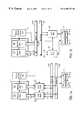
- FIG. 4shows a third embodiment according to the present invention.
- a memory block 1is coupled by a 64 bit read bus 1 a and a 64 bit write bus 1 b with a coupling unit 42 of a first 64 bit bus 46 .
- a single bi-directional buscan be used.
- the two memory bankscan be addressed with either a common address signal generated by a memory address and select unit (not shown) or an individual address signal for each memory bank generated by the memory address and select unit.
- memory address and select unitprovides a address incrementer as will be explained later.
- a second coupling unit 44couples bus 46 with respective 64 bit read and write buses of an address register file 8 .
- a ′indicates the same elements on the data register file side.
- Interface 4comprises a second bus 47 with coupling units 43 and 45 . Between the two busses 46 and 47 a bridge is provided. This bridge 41 is controllable and can couple both busses 46 and 47 . A switch control unit 3 is provided which controls the coupling units 42 , 43 , 44 , and 45 , the bridge 41 and an external interface 7 which can couple external devices through busses 7 a, 7 b, and 7 c.
- FIG. 4shows basically the same elements as FIG. 3 .
- a bridge unit 41is provided. If this bridge unit 41 is activated by switch control 3 , then only up to 2 32 bit long words or 4 16 bit words can be transferred to or from either address register file 8 or data register file 8 ′. Also, only either memory block 1 or memory block 1 ′ can be source or destination in this mode. On the other hand both memory blocks 1 and 1 ′ can form a single memory with consecutive memory addresses and data can be transferred from any location within this memory to any register in the register files 8 and 8 ′. Also, the external interface 7 can provide data which can be transferred to either register file.
- an additional internal interface(not shown), for example, coupled with bus 46 or 47 , can be provided to transfer data from or to other on-chip devices.
- Bridge 41thereby selects the way the data is routed which can be from or to either internal memory bank 1 , 1 ′ to or from the register files 8 , 8 ′, the external interface 7 or internal interface.
- the bridge 41allows a plurality of combinations.
- the bridge 41is deactivated then the content of two 32 bit registers in the address register file and of two 32 bit registers in the data register file can be transferred within one single cycle from or to the memory subsystem 1 , 1 ′.
- Thisis very advantageous in case of a context switch where depending upon implementation the content of a number of registers has to be stored and restored. For example, if a context consists of four data and four address registers a context switch with an embodiment according to FIG. 4 takes only 2 cycles for storing and two cycles for restoring the respective registers.
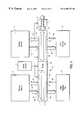
- FIG. 5shows an embodiment of one side of interface 4 including, for example, coupling units 42 , bus 46 , and coupling unit 44 .
- Memory block 1is divided into four memory towers or banks 101 , 102 , 103 , and 104 .
- Bus 46is divided into four 16 bit sub-busses 46 a, 46 b, 46 c, and 46 d. Each memory tower has a 16 bit data input/output port 101 a, 102 a, 103 a, and 104 a.
- Port 101 ais coupled with sub-bus 46 b and sub-bus 46 d.
- Port 102 ais coupled with sub-bus 46 a and sub-bus 46 c.
- Port 103 ais coupled with sub-bus 46 b and sub-bus 46 d.
- Port 104 ais coupled with sub-bus 46 a and sub-bus 46 c.
- Four 16 bit coupling busses 801 , 802 , 803 , and 804are provided.
- Coupling bus 801is coupled with sub-bus 46 a and 46 b.
- Coupling bus 802is coupled with sub-bus 46 b and 46 c.
- Coupling bus 803is coupled with sub-bus 46 c and 46 d.
- Coupling bus 804is coupled with sub-bus 46 d and 46 a.
- Each dot in FIG. 5indicates a coupling of each of the 16 lines of a port or coupling bus with one of the 16 respective lines of the sub-bus. In the upper right corner of FIG.
- FIG. 5an embodiment comprising tri-state buffers for a single bus line is shown.
- the input of a first tri-state driver 48is connected with one line of an input/output port of memory sub-system 1 . Its respective output line is connected to the respective line of bus 46 .
- a second tri-state driver 49is provided. Its input is connected to the same line of bus 46 and its output is connected with the same port of memory subsystem 1 .
- This embodimentshows bi-directional busses. Of course, unidirectional busses can be used as well.
- Memory 1comprises even and odd memory towers each having a port.
- the register file 8comprises a plurality of registers, whereby a number of registers are accessible in parallel.
- the register filehas a bit width which is at least equal to the sum of the bit width of each memory tower port, for example, if four memory towers each having a 16 bit port are used, then the register file 8 comprises at least two 32 bit registers or four 16 bit registers being accessible in parallel.
- the register file interfaceforms a multiple n-bit interface to said register file.
- the coupling buscomprises even and odd sub-busses, whereby first couplers are bi-directional tri-state drivers coupling each odd memory tower with each even sub-bus and each even memory tower with each even sub-bus and whereby the second couplers couple the sub-busses with the register file interface in such a way, that said port of any memory tower can be coupled with any n-bit part of said register file interface.
- each memory tower 101 , 102 , 103 , 104could be selectively coupled with each sub-bus and each coupling bus 801 , 802 , 803 , and 804 would be fixedly coupled with one of the sub-busses 46 a, 46 b, 46 c, 46 d, respectively.
- a further embodimentwould provide all selective couplings between coupling busses 801 , 802 , 803 , 804 and the sub-busses 46 a, 46 b, 46 c, 46 d and fixed connections between the memory towers 101 , 102 , 103 , 104 and the sub-busses 46 a, 46 b, 46 c, 46 d.
- Port 103 ais coupled sub-bus 46 b
- port 104 ais coupled with sub-bus 46 c
- port 101 ais coupled with sub-bus 46 d
- port 102 ais coupled with sub-bus 46 a.
- sub-bus 46 bis coupled with coupling bus 801
- sub-bus 46 cis coupled with coupling bus 802
- sub-bus 46 dis coupled with coupling bus 803
- sub-bus 46 ais coupled with coupling bus 804 .
- FIG. 6 and FIG. 7This access scheme allows access to any unaligned 64 bit data stored within a addressed memory portion of this 4 bank memory block. This type of access is the most common case which usually would need 2 cycles, for example, if a 64 bit data begins in memory bank 102 and ends in memory bank 101 , as shown in FIG. 6, then during a first cycle memory banks 102 , 103 , and 104 would output their data at address X and during a second cycle memory bank 101 outputs its data at address X+8 (bytewise addressing).
- FIG. 6shows an access scheme which allows access of unaligned data in a memory block with a plurality of memory banks within a single cycle.
- FIG. 6are again 4 memory banks 101 . 102 , 103 , and 104 with respective input/output ports 101 a, 102 a, 103 a, and 104 a shown.
- Each bankis addressed by address and select unit 9 by the upper address bit lines 90 which form the main address part of a respective address which addresses a 32 bit data portion of each bank 101 , 102 , 103 , and 104 .
- the 32 bit data portionconsists of two 16 bit memory cells 101 b, 101 c in memory bank 101 , 102 b, 102 c in memory bank 102 , 103 b, 103 c in memory bank 103 , and 104 b, 104 c in memory bank 104 .
- Data in memory block 1are stored in a sequential order such that memory cells 101 b, 102 b, 103 b, 104 b, 101 c, 102 c, 103 c, 104 c, etc. form consecutive memory cells within memory block 1 .
- memory cells 101 b, 102 b, 103 b, and 104 bcontain the upper data part and memory cells 101 c, 102 c, 103 c, and 104 c contain the lower data part of a 128 bit data word.
- Special address bit lines 91 , 92 , 93 , 94are used to select individually upper or lower memory cells in each bank 101 , 102 , 103 , and 104 . For example, as shown in FIG. 6, if unaligned 64 bit data start in memory bank 102 and end in memory bank 101 indicated by the shaded memory cells 102 b, 103 b, 104 b, and 101 c.
- Address and select unit 9selects these memory cells through address lines 90 , 91 , 92 , 93 , and 94 .
- Ports 101 a, 102 a, 103 a, and 104 athen carry the unaligned 64 bit data word which will be aligned through interface 4 as described above.
- FIG. 7shows a second embodiment of memory block 1 .
- two memory banks 105 and 106are provided. Each memory bank is organized in 64 bits.
- Bank 105contains the “upper/lower” data and is addresses by address lines 95 through memory address and select unit 9 to output 64 bit in parallel.
- Bank 106contains the “lower/upper” data and is addressed by address lines 96 through unit 9 to output also 64 bit in parallel.
- Address lines 95 and 96can be partly identical, for example only the least significant bit is handled differently. Depending on this least significant bit it is decided whether bank 105 or 106 contains the upper or lower part.
- Memory address and select unit 9provides an address incrementer to allow different addresses on address lines 95 and 96 .
- the 64 bit outputis fed in four 16 bit portions to four 2 ⁇ 16 multiplexers 107 , 108 , 109 , and 110 .
- the outputs of each multiplexer 101 a, 102 a, 103 a and 104 acarry the unaligned 64 bit data from memory 1 .
- the multiplexersare controlled by memory address and select unit 9 .
- the memory banks 105 and 106are organized in such a way, that data start in the first row of bank 105 , continue in the first row of bank 106 , followed by row 2 of bank 105 and so on. Again, for example, if unaligned 64 bit data start with the third 16 bit portion in memory bank 105 , as indicated by the shadowed memory cells in FIG.
- unit 9selects the same memory lines in bank 105 and 106 .
- multiplexers 107 , 108 , 109 , and 110the respective 16 bit portions of bank 105 or bank 106 are selected and fed to output ports 101 a, 102 a, 103 a, and 104 a.
- multiplexers 109 and 110select bank 105 and multiplexers 107 and 108 select bank 106 .
- the actual alignmentis done by interface 4 as described above.
- address lines 95 and 96must provide select lines for each memory cell within a row of memory banks 105 and 106 .
- FIG. 8shows an embodiment of the bridge unit 41 shown in FIG. 4 .
- Bus 46 and 47each are divided into four 16 bit sub-busses.
- Each line of each sub-bus of bus 46is coupled with the respective line of bus 47 by means of two tri-state drivers.
- FIG. 8shows only drivers for one of sixteen lines for each sub-bus.
- the tri-state driver pairs 450 , 451 ; 460 , 461 ; 470 , 471 ; 480 , 481each form a selectable bi-directional coupling element.
- Each drivereither functions as a read or write driver depending on the source and destination of the respective data.
- the upper or lower drivers of each linecan be enabled commonly or separately for each 16 bit sub-bus.
- each sub-busdifferent directions for each sub-bus are possible and, for example, 32 bit data can be written from memory block 1 to the data register 8 ′ and 32 bit data from memory 1 ′ to address register file 8 .
- Any other combinationis possible depending on the complexity of the bridge unit 41 .
- all top drivers 450 , 460 , 470 , and 480are enabled by a single signal and all bottom drivers 451 , 461 , 471 , and 481 are enabled by a second signal.
- FIG. 9Another embodiment of the memory interface is shown in FIG. 9 .
- a single memory block 120is provided.
- This memory block 120is organized in 128 bits.
- the interface between register file and memoryconsists of 32 double 2 ⁇ 1 multiplexers M 1 -M 32 as primary switches, an intermittent bus 490 and 8 barrel shifters as secondary switches.
- Each multiplexer M 1 -M 32contains two 2 ⁇ 1 multiplexers.
- the multiplexers M 1 -M 32are individually controlled by control signal C.
- Each bit cell output of an addressed row of memory block 120is coupled with an input of a multiplexer M 1 -M 32 . 4 multiplexers M 1 -M 4 ; M 5 -M 8 ; . . . M 29 -M 32 respectively are coupled with one of 8 barrel shifters B 1 -B 8 .
- the barrel shiftersare controlled by signal B.
- the barrel shifters B 1 -B 8output 64 bits in parallel which are fed to the register file.
- the 128 bits of each row of memory block 120are not stored in a consecutive order.
- the bit orderstarts with bit D 0 , D 8 , D 64 , D 72 , D 16 , D 24 , D 80 , D 88 , . . . D 48 , D 56 , D 112 , D 120 , . . . D 55 , D 63 , D 119 , D 127 .
- the orderis divided into eight blocks each having four 4 bit groups.
- the multiplexers M 1 -M 8select two data lines out of a 4 bit group, whereby either the first two and or the second two bits are selected, for example, multiplexer M 1 selects either data pair D 0 , D 8 or data pair D 64 , D 72 .
- the multiplexers M 1 -M 32are controlled separately, in other words each double multiplexer M 1 -M 32 is controlled by a different control line. Therefore, control signal C consists of at least 32 control lines.
- the output of all multiplexersform a 64 bit bus 490 .
- Eight 8-Bit barrel shifters B 1 -B 8form the secondary switches which switch the data on the 64 bit lines of bus 490 .
- Each barrel shifterperforms a left shift in increments of two bit depending on the control signal B which is formed by respective address signals.
- m0, 1, 2, 3, . . .
- Memory address and select unit(not shown) generate select signal A which selects the third row of memory 120 .
- select signal Aselects the third row of memory 120 .
- a switch control unit(not shown), which may be part of memory address and select unit, selects the second data pair of multiplexers M 1 , M 5 , M 9 , M 13 , M 17 , . . . M 29 and the first data pair of all other multiplexers.
- the input of barrel shifter B 1receives the following data signals: D 64 , D 72 , D 16 , D 24 , D 32 , D 40 , D 48 , and D 56 .
- Signal Bis common for all eight barrel shifters and indicates in this example to shift the data byte by one step. As mentioned above, one step is equal to a left shift by two bits.
- the output of barrel shifter B 1carries signals D 16 , D 24 , D 32 , D 40 , D 48 , D 56 , D 64 , D 72 . Even so the output of the barrel shifters B 1 -B 8 are not in the right order, there is a fixed relationship between each output line. Thus, no additional switching is necessary.
- the wiringselects the first bits of each barrel shifter B 1 -B 9 , followed by the second bits of each barrel shifter B 1 -B 9 , etc.
- the register filereceives a data word which is the aligned 64 bit word starting with bit D 16 , D 17 , D 18 , . . . D 79 .
- the principle of this embodimentis to provide multiplexers as first switches which select a predefined number of bits from the data provided by the memory in parallel to the respective internal bus.
- the second switchis used to bring the extracted bits in a predefined order.
- the second switchdoes not necessarily reduce the number of bits but does reorder the bits so that the relation of each consecutive bit is constant.
- the order of consecutive bits stored in the memorycan be arranged in many different ways and does not have to follow the order of the embodiment.
- Principle of the present inventionis to interleave or scramble the bytes, words, or long words stored in memory in an appropriate manner.
- a local multiplexingcan select the respective data bits.
- the write enable signalhas to be also interleaved to access the respective memory cells during a write cycle.
- the write enable signal for the first bytehas to go to bit 0 , 1 , 2 , 3 , . . . 7 which are not in consecutive order.
- the barrel shiftercan of course be realized by multiplexers or in any other known way.
- the output bit lines of barrel shifters B 1 -B 8do not have to be ordered before they are coupled with the register file. Depending on the size of each register this can also be done between the register file and the execution units as only execution units which actually manipulate the content of a register need the content of a data byte or word in order. Nevertheless, in a 32 bit microcomputer with 32 bit registers where a register might store 4 bytes, 2 words or 1 long word, it is advantageous to order the bits fed from the interface to the register file.
- any conventional memoryexternally or internally, can be used as the bit order in the memory is of no concern as long reading and writing lines use the same order. Thus, in case of a dual port memory with different port orders, a rewiring on either port has to be performed to ensure proper order of the memory content.
- FIG. 10shows a data transfer using the embodiment of FIG. 4 .
- Both memory banksare addressed by the same address signal generated by memory address and select unit 9 .
- Each memory bankhas a four 16 Bit-word wide interface, for example 64 bits.
- Bus 46 and bus 47each consist of four 16 Bit wide sub-busses 46 a, 46 b, 46 c, 46 d and 47 a, 47 b, 47 c, 47 d, respectively. If all four 16 Bit words are to be transferred from one memory bank to one of the register files 8 , 8 ′ the transfer takes place with or without usage of bridge 41 . In case of a boundary crossing data from both memory banks have to be transferred into one register file. This scenario is shown in FIG. 10 .
- the first two 16 Bit wordsare stored at the last two memory positions of the first memory bank 1 and the following two 16 Bit words are stored within the second memory bank 1 ′.
- the content of the last two memory cells of the first memory bankare transferred on sub-bus 46 a and 46 b.
- Bridge 41couples sub-bus 46 a with 47 a and sub-bus 46 b with 47 b.
- the second two 16 Bit wordsare transferred from the first two memory cells within the second memory bank 1 ′ onto sub-bus 47 c and 47 d, respectively. Through coupling bus 8 a ′ the four 16 Bit words are transferred into register file 8 ′.
- FIG. 11depicts a second scenario in which a crossing from the second memory bank 1 ′ to the first memory bank 1 takes place.
- memory address and select unit 9has to provide different addresses for each memory bank. Therefore, memory address and select unit 9 comprises an address incrementer to increment an address provided, for example, to memory bank 1 ′ for memory bank 1 . If, for example, four 16 Bit words are stored within the memory under an address, that, for example, the first 16 Bit word is stored in the last memory cell in one row of the second memory bank 1 ′, then the succeeding memory cells are located under a succeeding address in the first memory bank 1 .
- the incrementerincrements the address, in this example by 64, and provides the first memory bank 1 with the incremented address.
- the content of the last memory cell of the addressed row in the second memory bank 1 ′is transferred on sub-busses 47 a.
- the content of the first three memory cells of the row of the first memory bank 1 addressed by the incremented addressare transferred to sub-busses 46 b, 46 c, and 46 d, through the bridge to sub-busses 47 b, 47 c and 47 d.
- the transfer to register file 8 ′takes place in the same manner as described above.
- FIG. 12depicts a third scenario in which, for example, a context switch takes place.
- the purpose of such a transferis to load or store the content of a context represented by the content of a plurality of registers as quickly as possible.
- the bridge 41completely de-couples busses 42 from busses 43 .
- 64 bit from memory bank 1can be transferred to register file 8 in parallel with 64 bits from memory bank 1 ′ to register file 8 ′ or vice versa. Therefore, memory address and select unit 9 addresses both memory banks 1 and 1 ′ with usually the same address were the context content is stored or is to be stored to. External or internal interfaces are usually also de-coupled during such a process.
- FIGS. 10, 11 , and 12do not show the couplers 42 , 43 , 44 , and 45 according to FIG. 4 . for a better overview, only the different data paths are shown.
- FIG. 13shows an embodiment of a single bus line, for example, bus line 46 a.
- Transfer from memory or register file to the busline 46 ais established via two tristate inverters 150 and 156 .
- a simple logicconsisting of NOR gate 151 and 157 controlled by a clock signal 152 and respective logic signals 153 and 158 controls drivers 150 and 152 . If the drivers 150 and 156 are not enabled a special bus holder arrangement secures the status of the bus line in a defined manner.
- the bus holderconsists of a first inverter 154 whose input is coupled with bus line 46 a and whose output is coupled with the input of a second inverter 155 whose output is coupled with bus line 46 a.
- Inverter 155is preferably weak to avoid a unnecessary load on the bus line for one of the drivers 150 or 156 . Such an arrangement avoids congestion problems on a bus line as the bus line is only actively driven during the low phase of the clock signal 152 . During the high phase of the clock signal 152 drivers 150 and 156 are disabled. Thus, an improved signal flow can be achieved.
- FIG. 14shows an improvement of the bus holder.
- a first inverter 160is coupled with a second inverter 161 in series to hold a signal on a bus line.
- the second inverter 161is a strong driver but switched. This driver is only active when the clock signal 152 is high and no other driver is active. These two conditions are anded by an AND gate 162 whose output controls driver 161 .
Landscapes
- Engineering & Computer Science (AREA)
- Theoretical Computer Science (AREA)
- Physics & Mathematics (AREA)
- General Engineering & Computer Science (AREA)
- General Physics & Mathematics (AREA)
- Executing Machine-Instructions (AREA)
- Memory System (AREA)
Abstract
Description
Claims (16)
Priority Applications (4)
| Application Number | Priority Date | Filing Date | Title |
|---|---|---|---|
| US09/192,170US6405273B1 (en) | 1998-11-13 | 1998-11-13 | Data processing device with memory coupling unit |
| EP99116654AEP1001347A3 (en) | 1998-11-13 | 1999-08-26 | Data processing device with memory coupling unit |
| JP11323951AJP2000231535A (en) | 1998-11-13 | 1999-11-15 | Data processor having memory coupling unit |
| US10/141,996US20020129188A1 (en) | 1998-11-13 | 2002-05-08 | Data processing device with memory coupling unit |
Applications Claiming Priority (1)
| Application Number | Priority Date | Filing Date | Title |
|---|---|---|---|
| US09/192,170US6405273B1 (en) | 1998-11-13 | 1998-11-13 | Data processing device with memory coupling unit |
Related Child Applications (1)
| Application Number | Title | Priority Date | Filing Date |
|---|---|---|---|
| US10/141,996DivisionUS20020129188A1 (en) | 1998-11-13 | 2002-05-08 | Data processing device with memory coupling unit |
Publications (1)
| Publication Number | Publication Date |
|---|---|
| US6405273B1true US6405273B1 (en) | 2002-06-11 |
Family
ID=22708548
Family Applications (2)
| Application Number | Title | Priority Date | Filing Date |
|---|---|---|---|
| US09/192,170Expired - LifetimeUS6405273B1 (en) | 1998-11-13 | 1998-11-13 | Data processing device with memory coupling unit |
| US10/141,996AbandonedUS20020129188A1 (en) | 1998-11-13 | 2002-05-08 | Data processing device with memory coupling unit |
Family Applications After (1)
| Application Number | Title | Priority Date | Filing Date |
|---|---|---|---|
| US10/141,996AbandonedUS20020129188A1 (en) | 1998-11-13 | 2002-05-08 | Data processing device with memory coupling unit |
Country Status (3)
| Country | Link |
|---|---|
| US (2) | US6405273B1 (en) |
| EP (1) | EP1001347A3 (en) |
| JP (1) | JP2000231535A (en) |
Cited By (30)
| Publication number | Priority date | Publication date | Assignee | Title |
|---|---|---|---|---|
| US20020129188A1 (en)* | 1998-11-13 | 2002-09-12 | Siemens Microelectronics, Inc. | Data processing device with memory coupling unit |
| US20020199041A1 (en)* | 2001-06-21 | 2002-12-26 | Yamaha Corporation | Data storage with scrambling by crossing parallel bit bus |
| US6584537B1 (en)* | 2000-12-06 | 2003-06-24 | Lsi Logic Corporation | Data-cache data-path |
| US6633576B1 (en)* | 1999-11-04 | 2003-10-14 | William Melaragni | Apparatus and method for interleaved packet storage |
| US20040039952A1 (en)* | 2000-01-31 | 2004-02-26 | Ruban Kanapathippillai | Method and apparatus for power reduction in a digital signal processor integrated circuit |
| US20040044833A1 (en)* | 2002-08-29 | 2004-03-04 | Ryan Kevin J. | System and method for optimizing interconnections of memory devices in a multichip module |
| US6721295B1 (en)* | 2000-08-25 | 2004-04-13 | Texas Instruments Incorporated | Triple data system for high data rate communication systems |
| US20040078608A1 (en)* | 2001-04-02 | 2004-04-22 | Ruban Kanapathippillai | Method and apparatus for power reduction in a digital signal processor integrated circuit |
| US20040153592A1 (en)* | 2001-06-13 | 2004-08-05 | Nokia Corporation | Method for adapting a bus and a bus |
| US6779098B2 (en)* | 2001-01-24 | 2004-08-17 | Renesas Technology Corp. | Data processing device capable of reading and writing of double precision data in one cycle |
| US6823016B1 (en) | 1998-02-20 | 2004-11-23 | Intel Corporation | Method and system for data management in a video decoder |
| US20050147242A1 (en)* | 2002-07-10 | 2005-07-07 | Infineon Technologies Ag | Device and method for performing a cryptoalgorithm |
| US20060047891A1 (en)* | 2004-08-31 | 2006-03-02 | Ralph James | System and method for transmitting data packets in a computer system having a memory hub architecture |
| US20060200598A1 (en)* | 2004-04-08 | 2006-09-07 | Janzen Jeffery W | System and method for optimizing interconnections of components in a multichip memory module |
| US7146454B1 (en)* | 2002-04-16 | 2006-12-05 | Cypress Semiconductor Corporation | Hiding refresh in 1T-SRAM architecture |
| US7282947B2 (en) | 2003-06-11 | 2007-10-16 | Micron Technology, Inc. | Memory module and method having improved signal routing topology |
| US7289347B2 (en) | 2002-08-02 | 2007-10-30 | Micron Technology, Inc. | System and method for optically interconnecting memory devices |
| US7366864B2 (en) | 2004-03-08 | 2008-04-29 | Micron Technology, Inc. | Memory hub architecture having programmable lane widths |
| US7370134B2 (en) | 2004-03-25 | 2008-05-06 | Micron Technology, Inc. | System and method for memory hub-based expansion bus |
| US20080162802A1 (en)* | 2006-12-28 | 2008-07-03 | James Akiyama | Accessing memory using multi-tiling |
| US7461286B2 (en) | 2003-10-27 | 2008-12-02 | Micron Technology, Inc. | System and method for using a learning sequence to establish communications on a high-speed nonsynchronous interface in the absence of clock forwarding |
| US7489875B2 (en) | 2002-08-09 | 2009-02-10 | Micron Technology, Inc. | System and method for multiple bit optical data transmission in memory systems |
| US7546435B2 (en) | 2004-02-05 | 2009-06-09 | Micron Technology. Inc. | Dynamic command and/or address mirroring system and method for memory modules |
| US20130297858A1 (en)* | 2012-04-19 | 2013-11-07 | Stec, Inc. | Systems and methods for providing channel buffer in a solid-state device |
| US8589643B2 (en) | 2003-10-20 | 2013-11-19 | Round Rock Research, Llc | Arbitration system and method for memory responses in a hub-based memory system |
| US8866830B2 (en) | 2005-06-30 | 2014-10-21 | Intel Corporation | Memory controller interface for micro-tiled memory access |
| US20150163518A1 (en)* | 2013-12-10 | 2015-06-11 | Lenovo (Beijing) Limited | Electronic device and information processing method |
| US10187044B1 (en)* | 2016-08-29 | 2019-01-22 | Amazon Technologies, Inc. | Bistable-element for random number generation |
| US20190347223A1 (en)* | 2018-05-10 | 2019-11-14 | Micron Technology, Inc. | Semiconductor device with a time multiplexing mechanism for size efficiency |
| US20190347219A1 (en)* | 2018-05-09 | 2019-11-14 | Micron Technology, Inc. | Memory devices having a reduced global data path footprint and associated systems and methods |
Families Citing this family (10)
| Publication number | Priority date | Publication date | Assignee | Title |
|---|---|---|---|---|
| US6769046B2 (en)* | 2000-02-14 | 2004-07-27 | Palmchip Corporation | System-resource router |
| US7398347B1 (en)* | 2004-07-14 | 2008-07-08 | Altera Corporation | Methods and apparatus for dynamic instruction controlled reconfigurable register file |
| US7209405B2 (en)* | 2005-02-23 | 2007-04-24 | Micron Technology, Inc. | Memory device and method having multiple internal data buses and memory bank interleaving |
| US8332598B2 (en) | 2005-06-23 | 2012-12-11 | Intel Corporation | Memory micro-tiling request reordering |
| US7765366B2 (en) | 2005-06-23 | 2010-07-27 | Intel Corporation | Memory micro-tiling |
| US7558941B2 (en) | 2005-06-30 | 2009-07-07 | Intel Corporation | Automatic detection of micro-tile enabled memory |
| US8032688B2 (en)* | 2005-06-30 | 2011-10-04 | Intel Corporation | Micro-tile memory interfaces |
| US7747833B2 (en)* | 2005-09-30 | 2010-06-29 | Mosaid Technologies Incorporated | Independent link and bank selection |
| US8347026B2 (en)* | 2007-12-21 | 2013-01-01 | Panasonic Corporation | Memory device and memory device control method |
| JP5834178B2 (en)* | 2012-11-08 | 2015-12-16 | パナソニックIpマネジメント株式会社 | Semiconductor circuit bus system |
Citations (1)
| Publication number | Priority date | Publication date | Assignee | Title |
|---|---|---|---|---|
| US5307506A (en)* | 1987-04-20 | 1994-04-26 | Digital Equipment Corporation | High bandwidth multiple computer bus apparatus |
Family Cites Families (9)
| Publication number | Priority date | Publication date | Assignee | Title |
|---|---|---|---|---|
| JPH03186928A (en)* | 1989-12-16 | 1991-08-14 | Mitsubishi Electric Corp | data processing equipment |
| US5226142A (en)* | 1990-11-21 | 1993-07-06 | Ross Technology, Inc. | High performance register file with overlapping windows |
| WO1994003860A1 (en)* | 1992-08-07 | 1994-02-17 | Thinking Machines Corporation | Massively parallel computer including auxiliary vector processor |
| US6513125B1 (en)* | 1993-04-22 | 2003-01-28 | Analog Devices, Inc. | Multi-phase multi-access pipeline memory system in which the pipeline memory can decode addresses issued by one processor while simultaneously accessing memory array by other processor |
| JPH086760A (en)* | 1994-06-20 | 1996-01-12 | Hitachi Ltd | Data processing device |
| US5875470A (en)* | 1995-09-28 | 1999-02-23 | International Business Machines Corporation | Multi-port multiple-simultaneous-access DRAM chip |
| US5954811A (en)* | 1996-01-25 | 1999-09-21 | Analog Devices, Inc. | Digital signal processor architecture |
| US6343356B1 (en)* | 1998-10-09 | 2002-01-29 | Bops, Inc. | Methods and apparatus for dynamic instruction controlled reconfiguration register file with extended precision |
| US6405273B1 (en)* | 1998-11-13 | 2002-06-11 | Infineon Technologies North America Corp. | Data processing device with memory coupling unit |
- 1998
- 1998-11-13USUS09/192,170patent/US6405273B1/ennot_activeExpired - Lifetime
- 1999
- 1999-08-26EPEP99116654Apatent/EP1001347A3/ennot_activeWithdrawn
- 1999-11-15JPJP11323951Apatent/JP2000231535A/enactivePending
- 2002
- 2002-05-08USUS10/141,996patent/US20020129188A1/ennot_activeAbandoned
Patent Citations (1)
| Publication number | Priority date | Publication date | Assignee | Title |
|---|---|---|---|---|
| US5307506A (en)* | 1987-04-20 | 1994-04-26 | Digital Equipment Corporation | High bandwidth multiple computer bus apparatus |
Cited By (66)
| Publication number | Priority date | Publication date | Assignee | Title |
|---|---|---|---|---|
| US8483290B2 (en) | 1998-02-20 | 2013-07-09 | Intel Corporation | Method and system for data management in a video decoder |
| US20100111164A1 (en)* | 1998-02-20 | 2010-05-06 | Hungviet Nguyen | Method and System for Data Management in a Video Decoder |
| US7672372B1 (en) | 1998-02-20 | 2010-03-02 | Intel Corporation | Method and system for data management in a video decoder |
| US6823016B1 (en) | 1998-02-20 | 2004-11-23 | Intel Corporation | Method and system for data management in a video decoder |
| US20020129188A1 (en)* | 1998-11-13 | 2002-09-12 | Siemens Microelectronics, Inc. | Data processing device with memory coupling unit |
| US6633576B1 (en)* | 1999-11-04 | 2003-10-14 | William Melaragni | Apparatus and method for interleaved packet storage |
| US7287148B2 (en) | 2000-01-31 | 2007-10-23 | Intel Corporation | Unified shared pipeline allowing deactivation of RISC/DSP units for power saving |
| US20040039952A1 (en)* | 2000-01-31 | 2004-02-26 | Ruban Kanapathippillai | Method and apparatus for power reduction in a digital signal processor integrated circuit |
| US20040236896A1 (en)* | 2000-01-31 | 2004-11-25 | Ruban Kanapathippillai | Memory with memory clusters for power reduction in an integrated circuit |
| US20040078612A1 (en)* | 2000-01-31 | 2004-04-22 | Ruban Kanapathippillai | Methods for power reduction in a digital signal processor integrated circuit |
| US7233166B2 (en) | 2000-01-31 | 2007-06-19 | Intel Corporation | Bus state keepers |
| US7318115B2 (en) | 2000-01-31 | 2008-01-08 | Intel Corporation | IC memory complex with controller for clusters of memory blocks I/O multiplexed using collar logic |
| US6721295B1 (en)* | 2000-08-25 | 2004-04-13 | Texas Instruments Incorporated | Triple data system for high data rate communication systems |
| US6584537B1 (en)* | 2000-12-06 | 2003-06-24 | Lsi Logic Corporation | Data-cache data-path |
| US6779098B2 (en)* | 2001-01-24 | 2004-08-17 | Renesas Technology Corp. | Data processing device capable of reading and writing of double precision data in one cycle |
| US20040078608A1 (en)* | 2001-04-02 | 2004-04-22 | Ruban Kanapathippillai | Method and apparatus for power reduction in a digital signal processor integrated circuit |
| US20040153592A1 (en)* | 2001-06-13 | 2004-08-05 | Nokia Corporation | Method for adapting a bus and a bus |
| US20020199041A1 (en)* | 2001-06-21 | 2002-12-26 | Yamaha Corporation | Data storage with scrambling by crossing parallel bit bus |
| US7146454B1 (en)* | 2002-04-16 | 2006-12-05 | Cypress Semiconductor Corporation | Hiding refresh in 1T-SRAM architecture |
| US20050147242A1 (en)* | 2002-07-10 | 2005-07-07 | Infineon Technologies Ag | Device and method for performing a cryptoalgorithm |
| US8005212B2 (en)* | 2002-07-10 | 2011-08-23 | Infineon Technologies Ag | Device and method for performing a cryptoalgorithm |
| US7411807B2 (en) | 2002-08-02 | 2008-08-12 | Micron Technology, Inc. | System and method for optically interconnecting memory devices |
| US7289347B2 (en) | 2002-08-02 | 2007-10-30 | Micron Technology, Inc. | System and method for optically interconnecting memory devices |
| US7382639B2 (en) | 2002-08-02 | 2008-06-03 | Micron Technology, Inc. | System and method for optically interconnecting memory devices |
| US7489875B2 (en) | 2002-08-09 | 2009-02-10 | Micron Technology, Inc. | System and method for multiple bit optical data transmission in memory systems |
| US8190819B2 (en) | 2002-08-29 | 2012-05-29 | Micron Technology, Inc. | System and method for optimizing interconnections of memory devices in a multichip module |
| US20110055478A1 (en)* | 2002-08-29 | 2011-03-03 | Ryan Kevin J | System and method for optimizing interconnections of memory devices in a multichip module |
| US7836252B2 (en) | 2002-08-29 | 2010-11-16 | Micron Technology, Inc. | System and method for optimizing interconnections of memory devices in a multichip module |
| US20040044833A1 (en)* | 2002-08-29 | 2004-03-04 | Ryan Kevin J. | System and method for optimizing interconnections of memory devices in a multichip module |
| US7805586B2 (en) | 2002-08-29 | 2010-09-28 | Micron Technology, Inc. | System and method for optimizing interconnections of memory devices in a multichip module |
| US7557601B2 (en) | 2003-06-11 | 2009-07-07 | Micron Technology, Inc. | Memory module and method having improved signal routing topology |
| US7746095B2 (en) | 2003-06-11 | 2010-06-29 | Round Rock Research, Llc | Memory module and method having improved signal routing topology |
| US7282947B2 (en) | 2003-06-11 | 2007-10-16 | Micron Technology, Inc. | Memory module and method having improved signal routing topology |
| US8589643B2 (en) | 2003-10-20 | 2013-11-19 | Round Rock Research, Llc | Arbitration system and method for memory responses in a hub-based memory system |
| US7461286B2 (en) | 2003-10-27 | 2008-12-02 | Micron Technology, Inc. | System and method for using a learning sequence to establish communications on a high-speed nonsynchronous interface in the absence of clock forwarding |
| US7546435B2 (en) | 2004-02-05 | 2009-06-09 | Micron Technology. Inc. | Dynamic command and/or address mirroring system and method for memory modules |
| US7596675B2 (en) | 2004-03-08 | 2009-09-29 | Micron Technology, Inc. | Memory hub architecture having programmable lane widths |
| US20090319750A1 (en)* | 2004-03-08 | 2009-12-24 | Micron Technology, Inc. | Memory hub architecture having programmable lane widths |
| US9274991B2 (en) | 2004-03-08 | 2016-03-01 | Micron Technology, Inc. | Memory hub architecture having programmable lane widths |
| US7366864B2 (en) | 2004-03-08 | 2008-04-29 | Micron Technology, Inc. | Memory hub architecture having programmable lane widths |
| US8775764B2 (en) | 2004-03-08 | 2014-07-08 | Micron Technology, Inc. | Memory hub architecture having programmable lane widths |
| US8015384B2 (en) | 2004-03-08 | 2011-09-06 | Micron Technology, Inc. | Memory hub architecture having programmable lane widths |
| US7370134B2 (en) | 2004-03-25 | 2008-05-06 | Micron Technology, Inc. | System and method for memory hub-based expansion bus |
| US20110145463A1 (en)* | 2004-03-25 | 2011-06-16 | Round Rock Research, Llc | System and method for memory hub-based expansion bus |
| US7899969B2 (en) | 2004-03-25 | 2011-03-01 | Round Rock Research, Llc | System and method for memory hub-based expansion bus |
| US8019924B2 (en) | 2004-03-25 | 2011-09-13 | Round Rock Research, Llc | System and method for memory hub-based expansion bus |
| US8117371B2 (en) | 2004-03-25 | 2012-02-14 | Round Rock Research, Llc | System and method for memory hub-based expansion bus |
| US20060200598A1 (en)* | 2004-04-08 | 2006-09-07 | Janzen Jeffery W | System and method for optimizing interconnections of components in a multichip memory module |
| US8438329B2 (en) | 2004-04-08 | 2013-05-07 | Micron Technology, Inc. | System and method for optimizing interconnections of components in a multichip memory module |
| US7870329B2 (en) | 2004-04-08 | 2011-01-11 | Micron Technology, Inc. | System and method for optimizing interconnections of components in a multichip memory module |
| US7590797B2 (en) | 2004-04-08 | 2009-09-15 | Micron Technology, Inc. | System and method for optimizing interconnections of components in a multichip memory module |
| US8346998B2 (en) | 2004-08-31 | 2013-01-01 | Micron Technology, Inc. | System and method for transmitting data packets in a computer system having a memory hub architecture |
| US7392331B2 (en)* | 2004-08-31 | 2008-06-24 | Micron Technology, Inc. | System and method for transmitting data packets in a computer system having a memory hub architecture |
| US7596641B2 (en) | 2004-08-31 | 2009-09-29 | Micron Technology, Inc. | System and method for transmitting data packets in a computer system having a memory hub architecture |
| US20060047891A1 (en)* | 2004-08-31 | 2006-03-02 | Ralph James | System and method for transmitting data packets in a computer system having a memory hub architecture |
| US7949803B2 (en) | 2004-08-31 | 2011-05-24 | Micron Technology, Inc. | System and method for transmitting data packets in a computer system having a memory hub architecture |
| US8866830B2 (en) | 2005-06-30 | 2014-10-21 | Intel Corporation | Memory controller interface for micro-tiled memory access |
| US8878860B2 (en) | 2006-12-28 | 2014-11-04 | Intel Corporation | Accessing memory using multi-tiling |
| US20080162802A1 (en)* | 2006-12-28 | 2008-07-03 | James Akiyama | Accessing memory using multi-tiling |
| US20130297858A1 (en)* | 2012-04-19 | 2013-11-07 | Stec, Inc. | Systems and methods for providing channel buffer in a solid-state device |
| US20150163518A1 (en)* | 2013-12-10 | 2015-06-11 | Lenovo (Beijing) Limited | Electronic device and information processing method |
| US9298673B2 (en)* | 2013-12-10 | 2016-03-29 | Lenovo (Beijing) Limited | Electronic device and information processing method |
| US10187044B1 (en)* | 2016-08-29 | 2019-01-22 | Amazon Technologies, Inc. | Bistable-element for random number generation |
| US20190347219A1 (en)* | 2018-05-09 | 2019-11-14 | Micron Technology, Inc. | Memory devices having a reduced global data path footprint and associated systems and methods |
| US20190347223A1 (en)* | 2018-05-10 | 2019-11-14 | Micron Technology, Inc. | Semiconductor device with a time multiplexing mechanism for size efficiency |
| US10747693B2 (en)* | 2018-05-10 | 2020-08-18 | Micron Technology, Inc. | Semiconductor device with a time multiplexing mechanism for size efficiency |
Also Published As
| Publication number | Publication date |
|---|---|
| EP1001347A3 (en) | 2003-04-09 |
| EP1001347A2 (en) | 2000-05-17 |
| JP2000231535A (en) | 2000-08-22 |
| US20020129188A1 (en) | 2002-09-12 |
Similar Documents
| Publication | Publication Date | Title |
|---|---|---|
| US6405273B1 (en) | Data processing device with memory coupling unit | |
| EP0100943B1 (en) | Hierarchical memory system | |
| JP2642671B2 (en) | Digital crossbar switch | |
| US5761478A (en) | Programmable memory interface for efficient transfer of different size data | |
| US5961640A (en) | Virtual contiguous FIFO having the provision of packet-driven automatic endian conversion | |
| US6256253B1 (en) | Memory device with support for unaligned access | |
| EP0636987A2 (en) | Functional pipelined cache memory | |
| US11836099B2 (en) | Memory system with cached memory module operations | |
| US6041387A (en) | Apparatus for read/write-access to registers having register file architecture in a central processing unit | |
| EP1381957A2 (en) | Data processing apparatus and system and method for controlling memory access | |
| EP0166309A2 (en) | Memory chip for a hierarchical memory system | |
| JPS5998365A (en) | Plural simultaneous access type storage device | |
| KR960004457B1 (en) | Data transmission device | |
| WO1997045870A1 (en) | A microcontroller having an n-bit data bus width with less than n i/o pins and a method therefor | |
| JPH04306756A (en) | Data transfer system | |
| US20050180240A1 (en) | Method and system for fast memory access | |
| WO2004068362A1 (en) | Processor array | |
| US6901490B2 (en) | Read/modify/write registers | |
| US5774653A (en) | High-throughput data buffer | |
| US6401161B1 (en) | High speed bus interface for non-volatile integrated circuit memory supporting continuous transfer | |
| WO1989008293A1 (en) | Bit blitter with narrow shift register | |
| US5732011A (en) | Digital system having high speed buffering | |
| US20080162831A1 (en) | Management/circuit arrangement and memory management system | |
| JP3965620B2 (en) | Storage device, storage method, and data processing system | |
| US6442097B2 (en) | Virtual channel DRAM |
Legal Events
| Date | Code | Title | Description |
|---|---|---|---|
| AS | Assignment | Owner name:SIEMENS MICROELECTRONICS, INC., CALIFORNIA Free format text:ASSIGNMENT OF ASSIGNORS INTEREST;ASSIGNORS:FLECK, ROD G.;OBERLAENDER, KLAUS;BAROR, GIGY;AND OTHERS;REEL/FRAME:009608/0272;SIGNING DATES FROM 19981007 TO 19981103 | |
| STCF | Information on status: patent grant | Free format text:PATENTED CASE | |
| AS | Assignment | Owner name:INFINEON TECHNOLOGIES CORPORATION, CALIFORNIA Free format text:CHANGE OF NAME;ASSIGNOR:SIEMENS DRAM SEMICONDUCTOR CORPORATION;REEL/FRAME:013595/0145 Effective date:19990401 Owner name:INFINEON TECHNOLOGIES NORTH AMERICA CORP., CALIFOR Free format text:CHANGE OF NAME;ASSIGNOR:INFINEON TECHNOLOGIES CORPORATION;REEL/FRAME:013595/0076 Effective date:19990929 Owner name:SIEMENS DRAM SEMICONDUCTOR CORPORATION, CALIFORNIA Free format text:TRANSFER OF ASSETS;ASSIGNOR:SMI HOLDING LLC;REEL/FRAME:013595/0068 Effective date:19990330 Owner name:SMI HOLDING LLC, CALIFORNIA Free format text:MERGER;ASSIGNOR:SIEMENS MICROELECTRONICS, INC.;REEL/FRAME:013595/0062 Effective date:19990330 | |
| FPAY | Fee payment | Year of fee payment:4 | |
| FPAY | Fee payment | Year of fee payment:8 | |
| AS | Assignment | Owner name:INFINEON TECHNOLOGIES AG, GERMANY Free format text:ASSIGNMENT OF ASSIGNORS INTEREST;ASSIGNOR:INFINEON TECHNOLOGIES NORTH AMERICA CORP.;REEL/FRAME:029034/0824 Effective date:20120918 | |
| FPAY | Fee payment | Year of fee payment:12 |