US6404797B1 - Efficiency high power laser device - Google Patents
Efficiency high power laser deviceDownload PDFInfo
- Publication number
- US6404797B1 US6404797B1US09/409,603US40960399AUS6404797B1US 6404797 B1US6404797 B1US 6404797B1US 40960399 AUS40960399 AUS 40960399AUS 6404797 B1US6404797 B1US 6404797B1
- Authority
- US
- United States
- Prior art keywords
- reflector
- volume
- laser device
- semiconductor substrate
- gain medium
- Prior art date
- Legal status (The legal status is an assumption and is not a legal conclusion. Google has not performed a legal analysis and makes no representation as to the accuracy of the status listed.)
- Expired - Lifetime
Links
- 239000004065semiconductorSubstances0.000claimsdescription94
- 239000000758substrateSubstances0.000claimsdescription89
- 230000003287optical effectEffects0.000claimsdescription81
- 239000000463materialSubstances0.000claimsdescription51
- 239000010410layerSubstances0.000claimsdescription20
- 238000003892spreadingMethods0.000claimsdescription17
- OKTJSMMVPCPJKN-UHFFFAOYSA-NCarbonChemical compound[C]OKTJSMMVPCPJKN-UHFFFAOYSA-N0.000claimsdescription2
- 229910052799carbonInorganic materials0.000claimsdescription2
- 239000002356single layerSubstances0.000claimsdescription2
- 239000002019doping agentSubstances0.000claims2
- 238000000034methodMethods0.000abstractdescription22
- 230000005855radiationEffects0.000abstractdescription19
- 238000006243chemical reactionMethods0.000abstractdescription17
- 230000002269spontaneous effectEffects0.000abstractdescription9
- 239000013078crystalSubstances0.000description14
- 230000000694effectsEffects0.000description12
- 238000010521absorption reactionMethods0.000description11
- 229910003334KNbO3Inorganic materials0.000description9
- 238000005086pumpingMethods0.000description7
- 239000000835fiberSubstances0.000description5
- 230000006870functionEffects0.000description5
- 239000007787solidSubstances0.000description5
- 229910003327LiNbO3Inorganic materials0.000description4
- 230000008878couplingEffects0.000description4
- 238000010168coupling processMethods0.000description4
- 238000005859coupling reactionMethods0.000description4
- 238000002310reflectometryMethods0.000description4
- 229910001218Gallium arsenideInorganic materials0.000description3
- 230000008901benefitEffects0.000description3
- 230000015556catabolic processEffects0.000description3
- 238000006731degradation reactionMethods0.000description3
- 238000013461designMethods0.000description3
- 238000009826distributionMethods0.000description3
- 230000005284excitationEffects0.000description3
- 238000002347injectionMethods0.000description3
- 239000007924injectionSubstances0.000description3
- 238000004519manufacturing processMethods0.000description3
- 239000006096absorbing agentSubstances0.000description2
- 239000000956alloySubstances0.000description2
- 229910045601alloyInorganic materials0.000description2
- 238000003491arrayMethods0.000description2
- 201000009310astigmatismDiseases0.000description2
- 239000000969carrierSubstances0.000description2
- 239000011248coating agentSubstances0.000description2
- 238000000576coating methodMethods0.000description2
- 239000004020conductorSubstances0.000description2
- 239000011521glassSubstances0.000description2
- 239000012535impuritySubstances0.000description2
- 230000003993interactionEffects0.000description2
- 239000000203mixtureSubstances0.000description2
- 238000001020plasma etchingMethods0.000description2
- 239000011149active materialSubstances0.000description1
- 230000006978adaptationEffects0.000description1
- 238000004458analytical methodMethods0.000description1
- 230000004888barrier functionEffects0.000description1
- BJQHLKABXJIVAM-UHFFFAOYSA-Nbis(2-ethylhexyl) phthalateChemical compoundCCCCC(CC)COC(=O)C1=CC=CC=C1C(=O)OCC(CC)CCCCBJQHLKABXJIVAM-UHFFFAOYSA-N0.000description1
- 230000008859changeEffects0.000description1
- 238000005253claddingMethods0.000description1
- 239000003086colorantSubstances0.000description1
- 238000004891communicationMethods0.000description1
- 238000004590computer programMethods0.000description1
- 230000007423decreaseEffects0.000description1
- 230000003247decreasing effectEffects0.000description1
- 230000001419dependent effectEffects0.000description1
- 238000000151depositionMethods0.000description1
- 239000003989dielectric materialSubstances0.000description1
- 238000009792diffusion processMethods0.000description1
- 238000005516engineering processMethods0.000description1
- 238000005530etchingMethods0.000description1
- 238000002474experimental methodMethods0.000description1
- 239000000284extractSubstances0.000description1
- 238000000605extractionMethods0.000description1
- 230000002349favourable effectEffects0.000description1
- 238000010438heat treatmentMethods0.000description1
- 150000002500ionsChemical class0.000description1
- 239000004973liquid crystal related substanceSubstances0.000description1
- 230000005055memory storageEffects0.000description1
- UKDIAJWKFXFVFG-UHFFFAOYSA-Npotassium;oxido(dioxo)niobiumChemical compound[K+].[O-][Nb](=O)=OUKDIAJWKFXFVFG-UHFFFAOYSA-N0.000description1
- 238000012545processingMethods0.000description1
- 230000009467reductionEffects0.000description1
- 229910052710siliconInorganic materials0.000description1
- 238000005476solderingMethods0.000description1
- 239000000243solutionSubstances0.000description1
- 230000003595spectral effectEffects0.000description1
- 230000004936stimulating effectEffects0.000description1
- XOLBLPGZBRYERU-UHFFFAOYSA-Ntin dioxideChemical compoundO=[Sn]=OXOLBLPGZBRYERU-UHFFFAOYSA-N0.000description1
- 229910001887tin oxideInorganic materials0.000description1
- 230000007704transitionEffects0.000description1
- 238000003466weldingMethods0.000description1
Images


Classifications
- H—ELECTRICITY
- H04—ELECTRIC COMMUNICATION TECHNIQUE
- H04N—PICTORIAL COMMUNICATION, e.g. TELEVISION
- H04N9/00—Details of colour television systems
- H04N9/12—Picture reproducers
- H04N9/31—Projection devices for colour picture display, e.g. using electronic spatial light modulators [ESLM]
- H04N9/3141—Constructional details thereof
- H04N9/315—Modulator illumination systems
- H—ELECTRICITY
- H01—ELECTRIC ELEMENTS
- H01S—DEVICES USING THE PROCESS OF LIGHT AMPLIFICATION BY STIMULATED EMISSION OF RADIATION [LASER] TO AMPLIFY OR GENERATE LIGHT; DEVICES USING STIMULATED EMISSION OF ELECTROMAGNETIC RADIATION IN WAVE RANGES OTHER THAN OPTICAL
- H01S5/00—Semiconductor lasers
- H01S5/04—Processes or apparatus for excitation, e.g. pumping, e.g. by electron beams
- H01S5/042—Electrical excitation ; Circuits therefor
- H01S5/0425—Electrodes, e.g. characterised by the structure
- H01S5/04256—Electrodes, e.g. characterised by the structure characterised by the configuration
- H—ELECTRICITY
- H01—ELECTRIC ELEMENTS
- H01S—DEVICES USING THE PROCESS OF LIGHT AMPLIFICATION BY STIMULATED EMISSION OF RADIATION [LASER] TO AMPLIFY OR GENERATE LIGHT; DEVICES USING STIMULATED EMISSION OF ELECTROMAGNETIC RADIATION IN WAVE RANGES OTHER THAN OPTICAL
- H01S5/00—Semiconductor lasers
- H01S5/10—Construction or shape of the optical resonator, e.g. extended or external cavity, coupled cavities, bent-guide, varying width, thickness or composition of the active region
- H01S5/18—Surface-emitting [SE] lasers, e.g. having both horizontal and vertical cavities
- H01S5/183—Surface-emitting [SE] lasers, e.g. having both horizontal and vertical cavities having only vertical cavities, e.g. vertical cavity surface-emitting lasers [VCSEL]
- H01S5/18308—Surface-emitting [SE] lasers, e.g. having both horizontal and vertical cavities having only vertical cavities, e.g. vertical cavity surface-emitting lasers [VCSEL] having a special structure for lateral current or light confinement
- H—ELECTRICITY
- H01—ELECTRIC ELEMENTS
- H01S—DEVICES USING THE PROCESS OF LIGHT AMPLIFICATION BY STIMULATED EMISSION OF RADIATION [LASER] TO AMPLIFY OR GENERATE LIGHT; DEVICES USING STIMULATED EMISSION OF ELECTROMAGNETIC RADIATION IN WAVE RANGES OTHER THAN OPTICAL
- H01S2301/00—Functional characteristics
- H01S2301/16—Semiconductor lasers with special structural design to influence the modes, e.g. specific multimode
- H01S2301/166—Single transverse or lateral mode
- H—ELECTRICITY
- H01—ELECTRIC ELEMENTS
- H01S—DEVICES USING THE PROCESS OF LIGHT AMPLIFICATION BY STIMULATED EMISSION OF RADIATION [LASER] TO AMPLIFY OR GENERATE LIGHT; DEVICES USING STIMULATED EMISSION OF ELECTROMAGNETIC RADIATION IN WAVE RANGES OTHER THAN OPTICAL
- H01S3/00—Lasers, i.e. devices using stimulated emission of electromagnetic radiation in the infrared, visible or ultraviolet wave range
- H01S3/10—Controlling the intensity, frequency, phase, polarisation or direction of the emitted radiation, e.g. switching, gating, modulating or demodulating
- H01S3/102—Controlling the intensity, frequency, phase, polarisation or direction of the emitted radiation, e.g. switching, gating, modulating or demodulating by controlling the active medium, e.g. by controlling the processes or apparatus for excitation
- H01S3/1022—Controlling the intensity, frequency, phase, polarisation or direction of the emitted radiation, e.g. switching, gating, modulating or demodulating by controlling the active medium, e.g. by controlling the processes or apparatus for excitation by controlling the optical pumping
- H—ELECTRICITY
- H01—ELECTRIC ELEMENTS
- H01S—DEVICES USING THE PROCESS OF LIGHT AMPLIFICATION BY STIMULATED EMISSION OF RADIATION [LASER] TO AMPLIFY OR GENERATE LIGHT; DEVICES USING STIMULATED EMISSION OF ELECTROMAGNETIC RADIATION IN WAVE RANGES OTHER THAN OPTICAL
- H01S3/00—Lasers, i.e. devices using stimulated emission of electromagnetic radiation in the infrared, visible or ultraviolet wave range
- H01S3/10—Controlling the intensity, frequency, phase, polarisation or direction of the emitted radiation, e.g. switching, gating, modulating or demodulating
- H01S3/106—Controlling the intensity, frequency, phase, polarisation or direction of the emitted radiation, e.g. switching, gating, modulating or demodulating by controlling devices placed within the cavity
- H01S3/108—Controlling the intensity, frequency, phase, polarisation or direction of the emitted radiation, e.g. switching, gating, modulating or demodulating by controlling devices placed within the cavity using non-linear optical devices, e.g. exhibiting Brillouin or Raman scattering
- H01S3/109—Frequency multiplication, e.g. harmonic generation
- H—ELECTRICITY
- H01—ELECTRIC ELEMENTS
- H01S—DEVICES USING THE PROCESS OF LIGHT AMPLIFICATION BY STIMULATED EMISSION OF RADIATION [LASER] TO AMPLIFY OR GENERATE LIGHT; DEVICES USING STIMULATED EMISSION OF ELECTROMAGNETIC RADIATION IN WAVE RANGES OTHER THAN OPTICAL
- H01S5/00—Semiconductor lasers
- H01S5/04—Processes or apparatus for excitation, e.g. pumping, e.g. by electron beams
- H01S5/041—Optical pumping
- H—ELECTRICITY
- H01—ELECTRIC ELEMENTS
- H01S—DEVICES USING THE PROCESS OF LIGHT AMPLIFICATION BY STIMULATED EMISSION OF RADIATION [LASER] TO AMPLIFY OR GENERATE LIGHT; DEVICES USING STIMULATED EMISSION OF ELECTROMAGNETIC RADIATION IN WAVE RANGES OTHER THAN OPTICAL
- H01S5/00—Semiconductor lasers
- H01S5/10—Construction or shape of the optical resonator, e.g. extended or external cavity, coupled cavities, bent-guide, varying width, thickness or composition of the active region
- H01S5/14—External cavity lasers
- H01S5/141—External cavity lasers using a wavelength selective device, e.g. a grating or etalon
- H—ELECTRICITY
- H01—ELECTRIC ELEMENTS
- H01S—DEVICES USING THE PROCESS OF LIGHT AMPLIFICATION BY STIMULATED EMISSION OF RADIATION [LASER] TO AMPLIFY OR GENERATE LIGHT; DEVICES USING STIMULATED EMISSION OF ELECTROMAGNETIC RADIATION IN WAVE RANGES OTHER THAN OPTICAL
- H01S5/00—Semiconductor lasers
- H01S5/10—Construction or shape of the optical resonator, e.g. extended or external cavity, coupled cavities, bent-guide, varying width, thickness or composition of the active region
- H01S5/18—Surface-emitting [SE] lasers, e.g. having both horizontal and vertical cavities
- H01S5/183—Surface-emitting [SE] lasers, e.g. having both horizontal and vertical cavities having only vertical cavities, e.g. vertical cavity surface-emitting lasers [VCSEL]
- H01S5/18386—Details of the emission surface for influencing the near- or far-field, e.g. a grating on the surface
- H01S5/18394—Apertures, e.g. defined by the shape of the upper electrode
Definitions
- CMOS lasersin common use today include edge-emitting diode lasers and vertical cavity surface emitting lasers (VCSELs).
- a semiconductor gain mediumfor example a quantum-well semiconductor structure, is formed on a surface of a semiconductor substrate.
- Cavity mirrorsare formed or otherwise positioned on opposite sides of the substrate, perpendicular to the substrate surfaces, to form a resonant cavity which includes the gain medium. Electrical or optical pumping of the gain medium generates a laser beam which propagates in a direction along the plane of the substrate.
- Edge-emitting lasersare among the most common semiconductor laser devices. Available commercially as individual units and in linear bar arrays, they are used, for example, as an optical pump source for pumping solid state lasers. High power, typically greater than a few hundred milliwatts, adaptations of edge-emitting lasers commonly operate in high order spatial modes and at multiple frequencies. This prevents their use in applications which require high power laser output in a single spatial mode and/or at a single frequency. Edge emitters also have a significant degree of astigmatism and a beam aspect ratio which is generally large, making it difficult to focus the beam to a small spot, which prevents their use in those applications which require a focused output beam. Poor beam quality in edge-emitting lasers also makes frequency doubling of the laser output using nonlinear optical materials difficult and inefficient.
- cavity mirrorsare formed or otherwise positioned on opposite faces of a semiconductor gain medium grown on a semiconductor substrate. Electrical or optical pumping generates a laser beam emitted in a direction orthogonal to the plane of the substrate.
- VCSELsfind application in optical communications and optical interconnect systems.
- VCSEL lasersare characterized by generally low fundamental spatial mode TEM 00 output powers, limited to about 8-10 milliwatts (mW) continuous wave (cw), and are further characterized by small fundamental spatial mode beam diameters, on the order of several micrometers ( ⁇ m). Larger area VCSEL emitters, with beam diameters on the order of 100 ⁇ m can produce output beams having a few hundred mW of cw output power.
- operation of conventional VCSELs at high power and large diametergenerally carries with it the penalty of an output beam having high-order spatial modes and multiple frequencies.
- an external cavity VCSEL configurationreferred to in the art as a vertical external cavity surface emitting laser (VECSEL)
- VECSELvertical external cavity surface emitting laser
- an external reflectorserves as the output coupler. External cavity VECSEL devices can provide higher fundamental spatial mode output power than VCSEL devices.
- a beam generated by the laseris subjected to frequency conversion or frequency doubling.
- Thisis accomplished by introducing a nonlinear material, for example KTP, KTN, KNbO 3 , and LiNbO 3 into the laser path.
- the frequency of a beam incident on the non-linear materialis converted to a second frequency.
- the non-linear materialsare referred to as “doubling crystals” where the property of the material is such that it serves to double the frequency of a beam traversing the crystal. Efficient frequency conversion by the material generally requires a high-intensity, single mode incident beam.
- Frequency doubling of semiconductor lasershas been demonstrated in the past to varying degrees of success using a doubling crystal mounted external to an edge-emitting diode laser cavity.
- the output beams from edge-emitting diode lasersare usually highly divergent and have significant aspect ratios as well as some degree of astigmatism which degrades the optical field intensity and phase front from that which is ideally required for efficient frequency doubling.
- Experimentshave been carried out in which the light from a diode laser is launched into an optical waveguide fabricated in a non-linear material in order to maintain the optical field intensity over some relatively long path length. This technique is generally complicated and uses relatively low power diode lasers which have sufficient beam quality to launch the laser light into the external waveguide.
- the Koslovsky configurationrequired frequency-locking of the single-frequency laser to the Fabry-Perot resonance of the ring cavity as well as matching the temperature of the non-linear crystal to both frequencies. This requires complicated crystal alignment and wavelength control circuitry to maintain frequency locking.
- the present inventionis directed to an apparatus and method for generating high power laser radiation in a single fundamental spatial mode, in a manner which overcomes the aforementioned limitations.
- the laser of the present inventionwhen configured in an external cavity, is especially amenable to frequency conversion of the output beam, as it provides beam power densities over suitable path lengths for efficient frequency conversion.
- the apparatuscomprises a resonant cavity defined between first and second partial reflectors.
- the geometry of the resonant cavitydefines a fundamental spatial or transverse cavity mode.
- a gain mediumis disposed within the resonant cavity, and a first volume of the gain medium is adapted to be energized by an external energy source. This causes spontaneous and stimulated energy emission to propagate in the gain medium in a direction transverse to the fundamental cavity mode.
- the transverse emissionoptically pumps a second volume of the gain medium about the first volume. When the intensity of the spontaneous emission is sufficiently high, inversion and gain are produced in the second volume.
- the energy within the first and second volumesis coupled into the fundamental cavity mode laser beam.
- the cavity mirrorsare selected to match the fundamental cavity mode to the cross-sectional diameter of the second volume. In this manner, the laser energy in the fundamental spatial mode is efficiently extracted from both first and second volumes of the gain medium. Similar results apply where the output energy is in a higher order spatial mode.
- the first volumeis substantially cylindrical and of cross sectional diameter D 1
- the second volumeis substantially an annulus of outer cross-sectional diameter D 2 and inner cross-sectional diameter D 1 , the first and second volumes being substantially cross-sectionally concentric.
- the gain mediumis preferably formed of a semiconductor material in a vertical cavity configuration.
- the gain mediummay be formed of a solid state material having an active ion which has absorption in the spectral region of the gain transition. Examples of such solid state materials include Er:glass, Yb:glass, and Yb:YAG.
- pump energywould be preferably generated by optical means, for example a diode laser.
- the gain mediumis formed on a semiconductor substrate at a first side and the first reflector is formed directly adjacent to the gain medium.
- the second reflectoris positioned at a second side of the semiconductor substrate, opposite to the first.
- the second reflectormay be monolithically grown on the semiconductor substrate, or it may be bonded to the semiconductor substrate by various techniques.
- a nonlinear crystalmay be placed in the optical cavity or external to the laser to change the laser output frequency.
- Suitable materials for nonlinear conversioninclude KTP, KTN, KNbO 3 , and LiNbO 3 and periodically-poled materials such as periodically-poled LiNbO 3 .
- a preferred embodiment of the present inventionis capable of generating intracavity circulating power levels in excess of 10 kW in a fundamental spatial mode for a 1 mm diameter beam. These levels are sufficient for producing harmonic conversion of the fundamental radiation in a non-linear material.
- frequency doubling in a semiconductor configuration using GalnAs gain mediaprovides a fundamental wavelength of 900 nm to 1100 nm and a frequency doubled output in the blue to green wavelengths.
- FIG. 1is a perspective and exploded view of a VECSEL laser configuration in accordance with the present invention.
- FIG. 2 ( a )is a cutaway side view of the configuration of FIG. 1 illustrating transverse propagation of spontaneous and stimulated emission from the first pumped volume into the second annular volume in accordance with the present invention.
- FIG. 2 ( b )is a cutaway side view of the configuration of FIG. 1 illustrating an nonlinear material being added to the present invention.
- FIG. 2 ( c )is a cutaway side view of the configuration of FIG. 1 illustrating a resistance-spreading layer and a saturable absorber layer being added to the present invention.
- FIG. 3is a perspective view of a VCSEL laser configuration illustrating the relationship of the first pumped volume and the second annular volume in accordance with the present invention.
- FIG. 4is a perspective illustration of an optical amplifier configuration in accordance with the present invention.
- FIG. 5is a side view of a coupling configuration for coupling output energy into a fiber-optic.
- FIG. 6is a side view of a VCSEL laser configuration having a second reflector/lens positioned directly adjacent to the semiconductor substrate.
- FIG. 7is a cutaway side view of an array of VCSEL lasers formed on two semiconductor substrates.
- FIG. 1is a perspective and exploded view of a preferred embodiment of the present invention, in a VECSEL configuration.
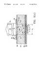
- the laser of FIG. 1includes a semiconductor substrate 20 , upon a first face of which is formed a semiconductor quantum-well gain region 22 .
- a first reflector 26for example a p-type Bragg reflector, is formed on the quantum-well region 22 .
- a second reflector 30is positioned opposite the first reflector 26 .
- the distance between the first and second reflectors 26 , 30 and their respective curvaturesdefine a fundamental cavity mode 60 .
- the second reflector 30is illustrated as one embodiment of the present having an external cavity mirror in FIG. 1 in accordance with a VECSEL configuration.
- the second reflector 30is layered directly adjacent to the second face of the substrate to provide a VCSEL configuration.
- the term “reflector” as used hereinincludes partially and/or fully reflective materials and/or surfaces.
- a surface 42 of the substrate 20 facing the second reflector 30preferably is treated with an anti-reflection coating 42 , such that any beam energy 60 traversing that interface will pass with minimal reflection, a desirable feature as is well known in the prior art.
- the resonant cavityis pumped electrically through an annular electrical contact 28 , causing current 38 to flow between the annular contact 28 and a circular contact 40 on opposite faces of the substrate 20 .
- the resulting current flow 38is generally conical in shape, the base 39 A of the cone being at the annular contact 28 and the peak of the cone 39 B being near contact 40 .
- the flow in the peak 39 Bis generally circular in cross section and energizes a substantially cylindrical first volume 44 of the gain region 22 , the first volume 44 being of a cross-sectional diameter D 1 .
- the diameter D 1is preferably substantially greater than the thickness of the gain region 22 .
- the excited gain region 22 of diameter D 1generates stimulated and spontaneous optical emission, represented by arrows 48 , which travels in a direction transverse to the propagation of the cavity laser beam.
- this transverse energy 48is absorbed in an annular second volume 46 surrounding the first pumped volume. This absorbed energy serves to pump the second volume 46 , providing gain and therefore power into the fundamental laser mode 60 .
- the adjacent regionis designed to absorb the stimulated emission (and also to a lesser extent the spontaneous emission), then the energy that otherwise would have been lost can be used to optically pump the second volume 46 to the extent that it will produce gain.
- the energy pumped into the second volume 46can be extracted in the orthogonal direction by adjusting the external mirror 30 to produce a mode waist equal to D 2 on the gain medium.
- the external cavity mirror 30will fix or “clamp” the gain in the total area defined by D 1 , and D 2 .
- There is a limit to the extent of the second volume 46as the degree of transverse pumping decreases with decreasing intensity away from the center of the pumped region. This limit is related to the dimension D 1 and the pumping intensity (electrical or optical) in the area defined by D 1 .
- the technique for designing a cavity which would provide a suitable radius of curvature R for the second reflector 30 and the suitable optical cavity length Lis well known in the art. See, for example, Herwig Kogelnik and Tingye Lee, “Beams, Modes, and Resonators”, CRC Handbook of Lasers, CRC Press, 1971, pg. 421-441.
- the second diameter D 2is a function of the excitation level and the diameter D 1 .
- the designwould be optimized for maximum output power limited by the circulating power density, which is limited by catastrophic degradation of the semiconductor, and the thermal power dissipation from the second diameter D 2 .
- the mode waist diameter for the cavitycould be matched, for example, by adjusting the cavity length L for a fixed radius of curvature R for the second reflector 30 .
- the second reflector 30is positioned directly adjacent to the annular contact 28 .
- a spaceis formed between the surface 42 of the semiconductor substrate 20 and the second reflector 30 .
- This arrangementmay be accomplished by bonding the second reflector 30 to the annular contact 28 , or by any other suitable techniques that are known to persons in the art.
- the second reflectormay be positioned directly adjacent to the surface 42 of the semiconductor substrate 20 and leaving no space therein between, as shown in FIG. 6, which will be explained in more detail.
- FIG. 2 ( c )shows an alternative embodiment of the present invention having a resistance-spreading layer 86 positioned adjacent to the top surface of the semiconductor substrate 20 , and a saturable absorber layer 84 positioned between the semiconductor substrate 20 and the quantum-well region 22 .
- FIG. 3is a perspective view of a laser in a VCSEL configuration in accordance with the present invention illustrating the relationship of the first pumped volume 44 and the second output volume 46 .
- the pumped first volume 44is of diameter D 1 in the region of the gain medium 22 .
- the transverse propagation of spontaneous and stimulated emission represented by arrows 48optically pumps or otherwise energizes an annular volume 46 surrounding the first volume 44 .
- the annular volume 46has an inner diameter of D 1 , and an outer diameter of D 2 and is substantially cross-sectionally concentric with the first volume 44 assuming a Gaussian beam distribution.
- the fundamental cavity modeis optimized to have a diameter approximately equal to the outer diameter D 2 of the second volume 46 , such that energy in both first and second volumes is captured and therefore contributes to the output beam 32 .
- Excitation of the first volume 44may occur by electrical or optical means.
- the laser cavity parametersare preferably adjusted to set the mode waist substantially equal to the diameter D 2 at the maximum operating power levels.
- the mode beam diameter on the laser chip w 1 and at the output mirror w 2is characterized by:
- the diameter of the fundamental laser modecan be made equal to the outer diameter D 2 of the second volume 46 , for example by adjusting the cavity length L for a specific radius of curvature R.
- the radius of curvature Rmay be selected for a specific range of cavity lengths L.
- a flat output coupler 30may be employed with a lens in the cavity, of appropriate geometry to achieve the same results. A physical lens or thermal lens may be used for this purpose.
- a preferred embodiment of a semiconductor laser devicemay comprise a multiple element quantum well structure or a single gain region having a total gain thickness equivalent to that of a multiple quantum well structure.
- a semiconductor laser devicemay comprise a multiple element quantum well structure or a single gain region having a total gain thickness equivalent to that of a multiple quantum well structure.
- at least several quantum wellswould be required to a laser device.
- at least ten quantum wellsare used in order to effectively overcome the optical losses due to optical absorption at the laser wavelength in the conductive substrate layer 20 .
- a typical thickness for a single quantum wellis approximately 8-10 nm.
- a laser structuresuch as a GalnAs gain region 22 having more than 3 quantum wells requires strain compensation in the gain region 22 , which may be accomplished by adding GaAsP layers to the gain region 22 , as is well known in the art.
- the total thickness or the number of quantum wellscan be increased to increase the gain to overcome all intracavity losses for efficient operation. This is limited only by the ability to uniformly grow such structures and by the practical threshold current density for such structures.
- Conventional VCSELstypically operate with only one or a few quantum wells between very high reflectivity mirrors. Such devices exhibit low optical gain and therefore would not operate as efficiently as the apparatus of the present invention.
- the electrical current or optical pump energy injected into the laser devicecan be provided by any of the well-known methods, for example in G.P. Agarwal, “Semiconductor Lasers”, The American Institute of Physics Press, pages 146-157.
- most of the injection current 38is directed into a circular region of a diameter equal to or less than the diameter D 1 of the fundamental spatial mode as defined by equations (1) and (2) above.
- the preferred embodiment of the present inventionemploys a VCSEL or VECSEL vertical cavity laser structure in which the total single pass gain is significantly lower than in edge-emitting lasers.
- the output from the vertical cavity device of the present inventionis distributed over a much larger circular beam area than in edge-emitting devices, for example several hundred times greater in area.
- the achievable intracavity circulating power density in a fundamental circular spatial modecan exceed several MW/cm 2 , limited only by catastrophic degradation at the semiconductor surface.
- the beamis confined to the waveguide of the diode cavity which makes frequency doubling difficult. Since the efficiency of frequency conversion is dependent on both the optical intensity and the length of the interaction region, frequency doubling of diode lasers is complicated and has been carried out in waveguide structures to maintain the field intensity of a sufficient long interaction length because the beam is substantially non-divergent within the optical laser cavity.
- a high beamprovides a more favorable frequency conversion situation for any conversion configuration outside of the cavity such as in the recently-studied periodically-poled nonlinear materials.
- the present inventioncan be operated in a pulsed, gain-switched, or mode-locked configuration to increase the optical power and therefore the nonlinear conversion efficiency.
- the present inventionapplies not only to harmonic frequency conversion, but also to sum and difference frequency generation.
- the non-linear materialincludes Fabry-Perot resonances such that the laser operates in a single frequency.
- FIG. 2 ( b )An exemplary configuration is illustrated in FIG. 2 ( b ), which includes an intracavity non-linear crystal 58 between the substrate 20 and external mirror 30 .
- the output power in the present inventioncan be magnified by increasing the diameter of the mode volume, as described above. Peak output power levels, for example in excess of 10 kW, can be generated from a gain area of one millimeter in diameter. Continuous cw output power levels may exceed 10 Watts from a single element device, limited only by thermal considerations.
- a second harmonic radiation which propagates in the backward directioncan additionally be absorbed in a semiconductor laser structure in such a way as to produce electrons and holes which migrate to the active gain region, thereby increasing the power of the fundamental laser radiation. This also has the effect of increasing efficiency of the second harmonic output as well as producing a single-ended output of harmonic radiation.
- the materials between the frequency doubling materials, such as a non-linear crystal, and the gain region 22must be transparent to the second harmonic radiation.
- a three-mirror cavitycould be used in which the nonlinear material is disposed in a position in which the harmonic radiation does not reflect back into the gain medium but exits through the middle mirror.
- a ring resonator configurationmay also be employed.
- Typical frequency doubling materials appropriate for conversion of infrared wavelengths into the visibleinclude periodically-poled LiNbO 3 , KTP, and KNbO 3 .
- KTPcan be phase matched to convert 1 ⁇ m radiation into green wavelengths
- KNbO 3can convert infrared radiation into blue wavelengths using GalnAs diode lasers operating in the 900 nm wavelength range.
- a focusing lenscan be positioned within the laser resonator defined by the mirrors 26 and 30 to increase the power density.
- the techniquewould allow use of very short lengths of nonlinear materials or nonlinear materials with lower nonlinear figures-of-merit.
- active crystal lengthscan be significantly less than 1 cm for the circulating power levels possible in the present configurations. Shorter nonlinear material lengths provide wider temperature and wavelength phase matching conditions. For KNbO 3 for example, a crystal length of 1 mm or less can provide a temperature phase matching bandwidth of more than several degrees Celsius and a wavelength bandwidth of several nanometers. Such broad acceptance ranges make the manufacture and operation of such devices significantly more practical.
- the wavelengthmay be controlled by the selection of the alloy composition of the gain medium material, while precision wavelength control is achievable with intracavity etalons or other wavelength controlling techniques well known in the art. Similar results apply to other nonlinear materials, including KTP.
- the non-linear material 58is positioned directly adjacent to the annular contact 28 and the second reflector 30 is then placed directly adjacent to the non-linear material 58 , as shown in FIG. 2 ( b ). Similar to the second reflector 30 shown in FIG. 2 ( a ), the non-linear material 58 in FIG. 2 ( b ) may be bonded to the annular contact 28 , or it may be coupled to the annular contact 28 by various techniques known in the art. Likewise, the second reflector 30 may be bonded to the nonlinear material 58 , or it may be coupled to the nonlinear material 58 by various technique known in the art. In an alternative embodiment of the present invention, the nonlinear material 58 may be placed directly adjacent to the surface 42 of the semiconductor substrate 20 and the second reflector 30 is placed directly adjacent to the nonlinear material 58 .
- the semiconductor gain region 22preferably comprises a multiple-element quantum well structure.
- a single gain region whose total gain thickness is equal to that of the multiple quantum well structuremay be employed.
- the number of wellscould be more than 50 .
- the limitis governed by the practical ability to grow large numbers of strain-free quantum well layers and strain compensating layers of GaAsP. In this case, a heterostructure may be a more effective choice.
- High-peak-power devicescould be made, for example, by using high-power Q-switched solid state lasers as pump sources.
- FIG. 2 ( a )illustrates a typical quantum-well device 22 formed on a semiconductor substrate 20 .
- a highly reflective mirror 26is grown on the back surface of the device to provide one of the mirrors of the laser resonator.
- the top cladding layerserves as a conductive contact which can be antireflection coated 42 and which has low optical absorption at the laser wavelength.
- a layer of electrically-conductive material with an optical bandgap greater than the second harmonic radiationserves as the conductive layer with a second layer, of thickness less than the diffusion length of carriers and transparent to the fundamental laser radiation, and absorbing the second harmonic radiation grown between the active material and the thick wide-bandgap material, would allow the optically excited carriers to diffuse into the gain region.
- the thick conductive materialmay comprise for example, deposited tin oxide.
- Single frequency operationmay be achieved, for example, by introducing an etalon in the cavity.
- the nonlinear crystal 58may also serve as a frequency selective element.
- the present inventionattractive to a range of applications including projection display, optical disc read and write, optical holographic memory storage, and bio-fluorescence sensors.
- three primary colorscould be generated.
- the blue wavelength and green wavelengthcould be produced by frequency doubling the output of GalnAs semiconductor lasers whose outputs could be selected in the wavelength range from 900 nm to more than 1100 nm.
- Appropriate frequency doubling materialsinclude KTP for the green wavelength and KNbO 3 for the blue wavelength.
- Powermay be scaled using arrays of such devices. Output power levels of several tens of Watts may be generated.
- the output couplersmay comprise an array of lithographically-produced binary optical mirrors or micromirrors whose positions are precisely aligned with the center of the diode laser emitting areas, as shown in FIG. 7 .
- a projection display system employing the present inventioncould be operated using various light valve devices such as liquid crystal spatial light modulators, micro-mirrors such as those sold by Texas Instruments, and grating deflector light valves such as those developed by Silicon Light Machines of Sunnyvale, Calif.
- light valve devicessuch as liquid crystal spatial light modulators, micro-mirrors such as those sold by Texas Instruments, and grating deflector light valves such as those developed by Silicon Light Machines of Sunnyvale, Calif.
- all elements of the light valvecould be illuminated by every laser source by allowing the individual laser beams to expand so they overlap in the far field. In this way, the failure of one element would not significantly degrade the operation of the system.
- Binary optical lensesmay be used to focus the laser light in a top-hat distribution onto each pixel of the light valve to make efficient use of all available laser radiation.
- FIG. 7shows an exploded cross-sectional side view of an embodiment of the array arrangement of the laser devices according to the present invention.
- An one or two-dimensional array of surface emitting laser devicesare formed in a first semiconductor substrate 90 , and a corresponding one or two-dimensional array of micro-reflectors are formed on a second semiconductor substrate 92 .
- the first and second semiconductor substrates 90 , 92are then coupled together by various techniques well known in the art, forming an one or two-dimensional array of VCSEL or VECSEL laser devices.
- Positions of the surface emitting laser devices and the micro-reflectors on respective semiconductor substrates 90 , 92are precisely defined so that each surface emitting laser device may be accurately coupled to a corresponding micro-reflector respectively when both substrates are coupled together.
- an optional nonlinear material 94may be positioned between the first and second substrate 90 , 92 for frequency selection.
- FIG. 4is a perspective illustration of the present invention configured as an optical amplifier 70 .
- the optical amplifier 70 configurationincludes a semiconductor substrate 20 , a semiconductor gain medium 22 , and a first reflector 26 .
- a second reflectoris not required as the optical amplifier 70 does not include a resonant cavity.
- a first volume 44 of the gain medium 22is pumped with electrical or optical energy 56 .
- the first volume 44is generally cross-sectionally circular, having a diameter D 1 . As described above, this causes transverse stimulated and spontaneous propagation of energy 48 into a second volume 46 about the first volume 44 .
- the second volume 46is substantially circular in cross-section, the diameter being D 2 .
- An incident beam 50 of diameter D 2 and of a first amplitudeis directed at the pumped region 46 , overlapping with and being energized by both the first volume 44 and second volume 46 .
- the incident beam 50reflects at mirror 26 and is released as an output beam 52 of similar diameter D 2 .
- the output beam 52is amplified by the energized gain region 46 and is therefore of higher intensity than the incident beam 50 .
- a plurality of such gain elementsmay be used to increase the total gain of the system.
- a plurality of such gain elementscan be arranged in series to each other.
- a plurality of mirrorsare arranged in series and are properly positioned to reflect the output beam 52 back to the next gain element.
- each gain elementAs a result, the incident beam 50 is amplified by each gain element to increase the total gain.
- the above-mentioned configurationmay apply to a plurality of VECSEL laser devices arranged in series to increase the total output power.
- each of the serially arranged VECSEL devicesmay have a single-quantum-well structure, and thus lower gain, while the overall output power of the above arrangement could still reach to a desirable level.
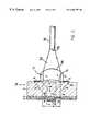
- a second alternative embodimentis illustrated in FIG. 5, representative of a side view of an optical coupling configuration.
- a single mirror/lens element 70includes a first concave face 72 which operates as a resonator mirror for VCSEL laser 78 , and a second convex face 74 which operates as a focusing element for directing laser radiation 32 into fiber-optic 76 .
- the VCSEL embodiment shown in FIG. 5is for illustrative purposes only. Alternative VECSEL embodiments may be used under the same principle of the present invention.
- the fiber-optic 76may comprise single-mode or multi-mode fiber, and is positioned at the focus of the laser radiation 32 such that the laser energy is directed substantially within the numerical aperture of the fiber.
- the reflectivity of the first surface 72is optimized to maximize output power from the laser device 78 , while the second surface 74 and the input surface 75 of fiber optic 76 are antireflection coated at the laser wavelength to minimize reflectivity.
- the mirror/lens element 70is aligned and positioned to maximize laser output power coupling, and is fixed using well-known techniques, including bonding, soldering, epoxying and/or laser welding.
- the fiberis then positioned to accept the focused radiation 32 and is set accordingly by any of the above techniques.
- This embodimentoffers the advantage of a reduction of the number of optical elements required to focus energy into a fiber by incorporating the function of a cavity mirror and an output lens into a single element.
- the doping level of each of these regionsshould be low enough to minimize the impurity absorption, the intra conduction band absorption and the free carrier absorption and, thus, to prevent excessive optical loss in these regions. If the doping levels in these regions are too high, the optical loss due to the free carrier absorption will lower the optical efficiency of the VECSEL or VCSEL laser devices.
- the VECSEL/VCSEL deviceshould have a low series resistance to have better electrical efficiency of the device.
- the series resistance of the VECSEL/VCSEL devicenamely, the semiconductor substrate 20 , the gain region 22 , and the P-type first reflector 26 .
- the resistance of the P-type first reflector 26could be substantially reduced by use of carbon doping to a concentration of approximately 1 ⁇ 10 19 cm ⁇ 3 , or by use of a graded alloy composition in the GaAs/GaAlAs p-type reflector layer 26 , to suppress the Schottky barriers at the interface.
- the resistance of the excited gain region 22is usually negligible, as compared to that of the semiconductor substrate 20 .
- the series resistance of the semiconductor substrate 20(normally, formed by a GaAs layer doped with n-type impurities having a concentration of between 2 ⁇ 10 16 cm ⁇ 3 and 1 ⁇ 10 18 cm ⁇ 3 and a thickness of between 10 ⁇ m and 200 ⁇ m) would dominate the total series resistance of the VECSEL/VCSEL device, if the resistance of the P-type first reflector 26 is designed to have a negligible resistance.
- the resistance of a semiconductor materialis a function of the electron concentration, i.e., the higher the electron concentration, the lower the resistance will be.
- the resistanceis found, in general, substantially independent to the thickness of the semiconductor substrate 20 .
- Higher doping concentrationwill also reduce the thermal dissipation of the VECSEL device, and a thinner substrate layer will reduce the distance to a heat sink (not shown).
- the thermal performance and the reliability of the VECSEL/VCSEL devicemay also be improved.
- the doping level of the semiconductor substrate 20as mentioned above, shouldn't be too high as to generate too much of the optical loss.
- the optimum doping level of the semiconductor substrateis therefore determined by balancing the optical efficiency against the electrical efficiency of the laser device.
- the thicker the semiconductor substrate 20the larger the optical loss due to the free carrier absorption effect will occur, as the stimulated optical emission from the excited gain region 22 will have to travel longer distance in the semiconductor substrate 20 before it could reach the second reflector 30 .
- the semiconductor substrate 20should be thick enough to be handled conveniently for processing but thin enough to have low intracavity free carrier absorption.
- One or both surfaces of the semiconductor substrate 20may also be optically polished to approximately one wavelength flatness over the wafer diameter, as is well known in the art.
- FIG. 6shows an alternative embodiment of the present invention.
- a reflective element 80is monolithically positioned on the semiconductor substrate 20 .
- the reflective element 80functions as a stable resonator for defining the fundamental emission mode of the VCSEL laser device of the present invention.
- the reflective element 80may also function as a lens element for focusing laser emission to be incorporated into the fiber-optic 76 shown in FIG. 5 .
- the reflective element 80is grown directly on the semiconductor substrate 20 by various deposition techniques well known in the art. Prior to forming the reflective element 80 , the surface of the semiconductor substrate 20 is configured to a predetermined radius R.
- the configuration of the substrate surfacemay be accomplished by various etching techniques well known in the art, e.g., by reactive ion etching, plasma etching or re-growth techniques.
- the reflective element 80is then monolithically formed on the surface of the semiconductor substrate 20 .
- the reflective surface of the element 80has a radius R directly adjacent to the substrate surface to couple the optical emission to the fundamental emission mode.
- the outer surface of the element 80may also have the similar radius R, or it may have a convex radius for focusing optical emission purposes.
- the reflective element 80may be formed by a n-type Bragg mirror or by a dielectric material, or both.
- the reflective element 80may be bonded to the semiconductor substrate 20 using flip-chip bonding techniques that are well known in the art, as compared to being monolithically grown on the semiconductor substrate 20 .
- the non-linear crystal 58may be positioned on the semiconductor substrate 20 between the semiconductor substrate 20 and the reflective element 80 to generate harmonics of the fundamental output laser wavelength.
- the non-linear crystal 58may be monolithically grown on the semiconductor substrate 20 , or it may be bonded to the semiconductor substrate 20 by various techniques.
- FIG. 2 ( c )shows another alternative embodiment of the present invention.
- the present inventionincludes a n-type resistance-spreading region 86 used to reduce current crowding effect commonly affecting most conventional VCSEL/VECSEL laser devices.
- a n-type resistance-spreading region 86used to reduce current crowding effect commonly affecting most conventional VCSEL/VECSEL laser devices.
- having an uniform current injection levelis critical to improve efficiency of extracting laser power in a fundamental emission mode.
- the current density at the edge of the optical emission aperture (i.e., around the edge of the annular contact 28 ) of the conventional VECSEL/VCSEL deviceis often higher than the current density at the center of the aperture.
- This phenomenonis called current crowding effect, which causes uneven distribution of current injection in the VECSEL/VCSEL device and reduces efficiency of its fundamental emission mode.
- current crowding effectis substantially minimized by various techniques recently developed, it remains an undesirable problem to most VECSEL/VCSEL devices.
- the above-mentioned parameters of the semiconductor GaAs substrate 20i.e., doped n-type to between 2 ⁇ 10 16 cm ⁇ 3 and 1 ⁇ 10 18 cm ⁇ 3 and having a thickness of between 10 ⁇ m and 200 ⁇ m, will substantially reduce the current crowding effect, while it still allows efficient extraction of the TEM 00 mode.
- the present inventionoffers an unique solution to further reduce the current crowding effect beyond that provided by the substrate parameters mentioned above by providing one or more heavily doped n-type resistance-spreading region(s) 86 to the VCSEL device, as shown in FIG. 2 ( c ).
- the resistance-spreading region 86is also applicable to VECSEL devices, although only the VCSEL device is shown in FIG.
- the resistance-spreading region 86is positioned at the top of the semiconductor substrate 20 directly adjacent to the annular contact 28 .
- This resistance-spreading regionmay be composed of a single layer with an n-type concentration of between 5 ⁇ 10 18 cm ⁇ 3 and 2 ⁇ 10 19 cm ⁇ 3 , or it could be composed of 10 or more thin layers each having an n-type concentration of approximately 5 ⁇ 10 18 cm ⁇ 3 to 2 ⁇ 10 19 cm ⁇ 3 and 30 nm to 75 nm wide separated by regions doped n-type of approximately 1 ⁇ 10 17 cm ⁇ 3 to 1 ⁇ 10 18 cm ⁇ 3 .
- the resistance-spreading region 86not only could reduce the current crowding effect, it would also reduce local heating and subsequent reflective index distortion phenomena that commonly associate with the current crowding effect. By providing a resistance-spreading region 86 , the present invention thus increases the fundamental mode emission efficiency of the VECSEL/VCSEL devices.
- Each of the thin layers of the resistance-spreading region 86 in the VECSEL/VCSEL deviceshould be located approximately at a node of the optical energy emission defined by the wavelength of the laser and the first and second reflectors 26 , 30 to minimize the free carrier absorption effect.
- the doping density of the semiconductor substrate 20may be reduced and the thickness of the same may be increased while still maintaining a good efficiency of the fundamental emission mode, if the resistance-spreading region 86 is added to the VECSEL device.
Landscapes
- Physics & Mathematics (AREA)
- Electromagnetism (AREA)
- Optics & Photonics (AREA)
- Condensed Matter Physics & Semiconductors (AREA)
- General Physics & Mathematics (AREA)
- Engineering & Computer Science (AREA)
- Multimedia (AREA)
- Signal Processing (AREA)
- Nonlinear Science (AREA)
- Plasma & Fusion (AREA)
- Lasers (AREA)
- Semiconductor Lasers (AREA)
- Optical Modulation, Optical Deflection, Nonlinear Optics, Optical Demodulation, Optical Logic Elements (AREA)
Abstract
Description
Claims (27)
Priority Applications (1)
| Application Number | Priority Date | Filing Date | Title |
|---|---|---|---|
| US09/409,603US6404797B1 (en) | 1997-03-21 | 1999-09-30 | Efficiency high power laser device |
Applications Claiming Priority (3)
| Application Number | Priority Date | Filing Date | Title |
|---|---|---|---|
| US4118597P | 1997-03-21 | 1997-03-21 | |
| US08/888,533US6243407B1 (en) | 1997-03-21 | 1997-07-07 | High power laser devices |
| US09/409,603US6404797B1 (en) | 1997-03-21 | 1999-09-30 | Efficiency high power laser device |
Related Parent Applications (1)
| Application Number | Title | Priority Date | Filing Date |
|---|---|---|---|
| US08/888,533Continuation-In-PartUS6243407B1 (en) | 1997-03-21 | 1997-07-07 | High power laser devices |
Publications (1)
| Publication Number | Publication Date |
|---|---|
| US6404797B1true US6404797B1 (en) | 2002-06-11 |
Family
ID=26717895
Family Applications (3)
| Application Number | Title | Priority Date | Filing Date |
|---|---|---|---|
| US08/888,533Expired - LifetimeUS6243407B1 (en) | 1997-03-21 | 1997-07-07 | High power laser devices |
| US09/409,825Expired - LifetimeUS6614827B1 (en) | 1997-03-21 | 1999-09-30 | High power laser |
| US09/409,603Expired - LifetimeUS6404797B1 (en) | 1997-03-21 | 1999-09-30 | Efficiency high power laser device |
Family Applications Before (2)
| Application Number | Title | Priority Date | Filing Date |
|---|---|---|---|
| US08/888,533Expired - LifetimeUS6243407B1 (en) | 1997-03-21 | 1997-07-07 | High power laser devices |
| US09/409,825Expired - LifetimeUS6614827B1 (en) | 1997-03-21 | 1999-09-30 | High power laser |
Country Status (16)
| Country | Link |
|---|---|
| US (3) | US6243407B1 (en) |
| EP (1) | EP0968552B1 (en) |
| JP (2) | JP4050328B2 (en) |
| KR (1) | KR100375850B1 (en) |
| AT (1) | ATE409362T1 (en) |
| AU (1) | AU732161B2 (en) |
| BR (1) | BR9808393A (en) |
| CA (1) | CA2284225C (en) |
| CZ (1) | CZ290895B6 (en) |
| DE (1) | DE69840043D1 (en) |
| HU (1) | HUP0001761A3 (en) |
| IL (1) | IL131977A (en) |
| NZ (1) | NZ337874A (en) |
| PL (1) | PL335834A1 (en) |
| RU (1) | RU2190910C2 (en) |
| WO (1) | WO1998043329A1 (en) |
Cited By (32)
| Publication number | Priority date | Publication date | Assignee | Title |
|---|---|---|---|---|
| WO2002089270A1 (en)* | 2001-04-27 | 2002-11-07 | Photodigm | Grating-outcoupled surface-emitting lasers with flared gain regions |
| WO2002089271A1 (en)* | 2001-04-27 | 2002-11-07 | Photodigm | Grating-outcoupled surface-emitting lasers using quantum wells |
| US20030138024A1 (en)* | 1999-12-22 | 2003-07-24 | New Focus, Inc. | Method & apparatus for optical transmission |
| US6628695B1 (en)* | 2002-03-07 | 2003-09-30 | The Board Of Trustees Of The Leland Stanford Junior University | Monolithically integrated mode-locked vertical cavity surface emitting laser (VCSEL) |
| US20030185261A1 (en)* | 2002-03-29 | 2003-10-02 | Knopp Kevin J. | Cavity mirror for optically-pumped vertical-cavity surface-emitting laser (VCSEL) |
| US6639928B2 (en)* | 2001-04-25 | 2003-10-28 | Commissariat A L'energie Atomique - Cea | Optic device comprising a plurality of resonant cavities of different lengths associated with different wavelengths |
| US6714575B2 (en)* | 2001-03-05 | 2004-03-30 | Photodigm, Inc. | Optical modulator system |
| WO2004021525A3 (en)* | 2002-09-02 | 2004-04-22 | Hentze Lissotschenko Patentver | Semiconductor laser device |
| US20040218641A1 (en)* | 1999-05-26 | 2004-11-04 | Ii-Vi Incorporated | Optical contacting method and apparatus |
| US20050083980A1 (en)* | 2003-08-29 | 2005-04-21 | Osram Opto Semiconductors Gmbh | Semiconductor laser with reduced heat loss |
| US6972400B2 (en)* | 2000-11-02 | 2005-12-06 | Raytheon Company | Multi-mode vibration sensor laser |
| EP1633026A1 (en)* | 2004-08-23 | 2006-03-08 | Osram Opto Semiconductors GmbH | Semiconductor component with a curved mirror and fabrication method of a semiconductor component having a curved semiconductor body |
| WO2006105258A2 (en) | 2005-03-30 | 2006-10-05 | Novalux, Inc. | Manufacturable vertical extended cavity surface emitting laser arrays |
| WO2006105249A2 (en) | 2005-03-30 | 2006-10-05 | Novalux, Inc. | Frequency stabilized vertical extended cavity surface emitting lasers |
| US20060285076A1 (en)* | 2005-06-20 | 2006-12-21 | Seiko Epson Corporation | Laser source device, display device, and projector |
| US20070127245A1 (en)* | 2005-12-06 | 2007-06-07 | 3M Innovative Properties Company | Illumination system incorporating collimated light source |
| US20070147458A1 (en)* | 2005-06-10 | 2007-06-28 | Novalux, Inc. | Cavity and packaging designs for arrays of vertical cavity surface emitting lasers with or without extended cavities |
| US20070291799A1 (en)* | 2006-06-16 | 2007-12-20 | Janne Konttinen | High power laser device |
| US20080232412A1 (en)* | 2003-12-22 | 2008-09-25 | Kiminori Mizuuchi | Surface-Emitting Laser and Laser Projector |
| US20090080063A1 (en)* | 2007-09-21 | 2009-03-26 | Hc Photonics Corp. | Array waveguide and light source using the same |
| US20090207873A1 (en)* | 2008-02-14 | 2009-08-20 | Michael Jansen | Electrically-Pumped Semiconductor Zigzag Extended Cavity Surface Emitting Lasers and Superluminescent Leds |
| US20090279579A1 (en)* | 2005-09-02 | 2009-11-12 | Kyoto University | Two-dimensional photonic crystal surface-emitting laser light source |
| US20090304039A1 (en)* | 2006-04-13 | 2009-12-10 | Osram Opto Semiconductors Gmbh | Optoelectronic semiconductor element |
| US20100238966A1 (en)* | 2009-03-17 | 2010-09-23 | Seiko Epson Corporation | Light source apparatus and projector |
| US20140211215A1 (en)* | 2011-08-09 | 2014-07-31 | Primesense Ltd. | Projectors of structured light |
| US20140376092A1 (en)* | 2013-06-19 | 2014-12-25 | Primesense Ltd. | Integrated structured-light projector |
| US20160197452A1 (en)* | 2010-02-02 | 2016-07-07 | Apple Inc. | Integrated structured-light projector |
| US10054430B2 (en) | 2011-08-09 | 2018-08-21 | Apple Inc. | Overlapping pattern projector |
| US10153614B1 (en) | 2017-08-31 | 2018-12-11 | Apple Inc. | Creating arbitrary patterns on a 2-D uniform grid VCSEL array |
| DE102023127804A1 (en)* | 2023-08-17 | 2025-02-20 | Ii-Vi Delaware, Inc. | SEMICONDUCTOR LASER ARRANGEMENT WITH THIN-FILM LITHIUM COMPOSITE WAVEGUIDE |
| US20250093012A1 (en)* | 2023-09-20 | 2025-03-20 | Nichia Corporation | Light-emitting module and cover structure |
| US12442509B2 (en)* | 2023-09-20 | 2025-10-14 | Nichia Corporation | Light-emitting module with cover member and light-transmissive member having higher hardness than cover member |
Families Citing this family (81)
| Publication number | Priority date | Publication date | Assignee | Title |
|---|---|---|---|---|
| JP2950302B2 (en)* | 1997-11-25 | 1999-09-20 | 日本電気株式会社 | Semiconductor laser |
| US6813291B2 (en)* | 1998-06-26 | 2004-11-02 | Coretek Inc | Tunable fabry-perot filter and tunable vertical cavity surface emitting laser |
| US6542527B1 (en) | 1998-08-27 | 2003-04-01 | Regents Of The University Of Minnesota | Vertical cavity surface emitting laser |
| US6285702B1 (en) | 1999-03-05 | 2001-09-04 | Coherent, Inc. | High-power external-cavity optically-pumped semiconductor laser |
| US5991318A (en)* | 1998-10-26 | 1999-11-23 | Coherent, Inc. | Intracavity frequency-converted optically-pumped semiconductor laser |
| EP1125349B1 (en) | 1998-10-26 | 2007-02-21 | Coherent, Inc. | High-power external-cavity optically-pumped semiconductor lasers |
| US6574255B1 (en) | 1999-03-05 | 2003-06-03 | Coherent, Inc. | High-power external-cavity optically-pumped semiconductor lasers |
| US6298076B1 (en) | 1999-03-05 | 2001-10-02 | Coherent, Inc. | High-power external-cavity optically-pumped semiconductor lasers |
| US7249328B1 (en)* | 1999-05-21 | 2007-07-24 | E-Numerate Solutions, Inc. | Tree view for reusable data markup language |
| US6370168B1 (en) | 1999-10-20 | 2002-04-09 | Coherent, Inc. | Intracavity frequency-converted optically-pumped semiconductor laser |
| US7043134B2 (en) | 1999-12-23 | 2006-05-09 | Spectalis Corp. | Thermo-optic plasmon-polariton devices |
| US6735234B1 (en)* | 2000-02-11 | 2004-05-11 | Giga Tera Ag | Passively mode-locked optically pumped semiconductor external-cavity surface-emitting laser |
| US6778582B1 (en) | 2000-03-06 | 2004-08-17 | Novalux, Inc. | Coupled cavity high power semiconductor laser |
| US6515305B2 (en)* | 2000-09-18 | 2003-02-04 | Regents Of The University Of Minnesota | Vertical cavity surface emitting laser with single mode confinement |
| US6853658B1 (en)* | 2000-12-14 | 2005-02-08 | Finisar Corporation | Optical logical circuits based on lasing semiconductor optical amplifiers |
| US6909536B1 (en)* | 2001-03-09 | 2005-06-21 | Finisar Corporation | Optical receiver including a linear semiconductor optical amplifier |
| US6507593B1 (en) | 2001-09-24 | 2003-01-14 | Coherent, Inc. | Step-tunable external-cavity surface-emitting semiconductor laser |
| US6714581B2 (en) | 2001-10-01 | 2004-03-30 | Christopher J. Corcoran | Compact phase locked laser array and related techniques |
| US7539232B1 (en) | 2001-10-01 | 2009-05-26 | Corcoran Christopher J | Compact phase locked laser array and related techniques |
| US6765725B1 (en) | 2001-10-11 | 2004-07-20 | Boston Laser, Inc. | Fiber pigtailed high power laser diode module with high brightness |
| US20030071269A1 (en)* | 2001-10-15 | 2003-04-17 | Tseng Ampere A. | Apparatus and method for laser selective bonding technique for making sealed or enclosed microchannel structures |
| KR100404043B1 (en)* | 2001-10-19 | 2003-11-03 | 주식회사 비첼 | Vertically integrated high-power surface-emitting laser diode and method of manufacturing the same |
| US7197059B2 (en)* | 2002-05-08 | 2007-03-27 | Melles Griot, Inc. | Short wavelength diode-pumped solid-state laser |
| US20040076204A1 (en) | 2002-10-16 | 2004-04-22 | Kruschwitz Brian E. | External cavity organic laser |
| US20040202223A1 (en)* | 2003-04-08 | 2004-10-14 | Eric Crosson | External cavity laser having improved single mode operation |
| CA2453760A1 (en)* | 2002-12-20 | 2004-06-20 | Spectalis Corp. | External-cavity lasers |
| EP1670933A4 (en)* | 2003-09-22 | 2008-01-23 | Snake Creek Lasers Llc | High densiity methods for producing diode-pumped micro lasers |
| US20070166852A1 (en)* | 2003-09-22 | 2007-07-19 | Snake Creek Lasers Llc | Diode-pumped microlasers including resonator microchips and methods for producing the same |
| US20070121689A1 (en)* | 2003-09-22 | 2007-05-31 | Snake Creek Lasers Llc | Methods for Producing Diode-Pumped Micro Lasers |
| EP1560306B1 (en)* | 2004-01-30 | 2014-11-19 | OSRAM Opto Semiconductors GmbH | VCSEL with optical filter |
| CN100474716C (en)* | 2004-05-28 | 2009-04-01 | 奥斯兰姆奥普托半导体有限责任公司 | Semiconductor laser component with surface emission perpendicular to the emission direction |
| DE102004040077A1 (en)* | 2004-05-28 | 2005-12-22 | Osram Opto Semiconductors Gmbh | Surface emitting semiconductor laser device having a vertical emission direction |
| KR101015499B1 (en)* | 2004-06-19 | 2011-02-16 | 삼성전자주식회사 | Laser pumping unit for semiconductor laser device and semiconductor laser device for generating a plurality of wavelengths |
| EP1608049B1 (en)* | 2004-06-19 | 2007-08-01 | Samsung Electronics Co., Ltd. | External cavity plural wavelength laser system |
| US20060083276A1 (en)* | 2004-09-28 | 2006-04-20 | Snake Creek Lasers, Llc. | Cryogenically cooled solid state lasers |
| KR101015500B1 (en)* | 2004-10-11 | 2011-02-24 | 삼성전자주식회사 | High power laser device with tunnel junction and laser pumping part for the laser device |
| EP1648060B1 (en)* | 2004-10-14 | 2008-07-23 | Samsung Electronics Co.,Ltd. | Funnel structure vertical external cavity surface-emitting laser (VECSEL) |
| KR100982421B1 (en)* | 2004-10-14 | 2010-09-15 | 삼성전자주식회사 | Surface-emitting high power laser device having a funnel-type current injection region |
| US7244028B2 (en) | 2004-12-14 | 2007-07-17 | Coherent, Inc. | Laser illuminated projection displays |
| US7355657B2 (en)* | 2004-12-14 | 2008-04-08 | Coherent, Inc. | Laser illuminated projection displays |
| KR100982423B1 (en)* | 2004-12-28 | 2010-09-15 | 삼성전자주식회사 | Surface-emitting laser element with dual channel current injection structure |
| JP2008530809A (en)* | 2005-02-17 | 2008-08-07 | コーニンクレッカ フィリップス エレクトロニクス エヌ ヴィ | All solid state UV laser system |
| KR100718128B1 (en)* | 2005-06-02 | 2007-05-14 | 삼성전자주식회사 | Surface-emitting laser combined with pump laser on a single heat sink |
| KR100738527B1 (en)* | 2005-07-13 | 2007-07-11 | 삼성전자주식회사 | Optically Pumped Semiconductor Lasers |
| DE102006010727B4 (en)* | 2005-12-05 | 2019-10-24 | Osram Opto Semiconductors Gmbh | Surface emitting semiconductor device with a tunnel junction |
| DE102006010728A1 (en) | 2005-12-05 | 2007-06-06 | Osram Opto Semiconductors Gmbh | Semiconductor component and laser device |
| JP2007258260A (en)* | 2006-03-20 | 2007-10-04 | Kyoto Univ | Two-dimensional photonic crystal surface-emitting laser |
| EP2036172A2 (en)* | 2006-06-16 | 2009-03-18 | Vitaly Shchukin | Coupled cavity ld with tilted wave propagation |
| US7421001B2 (en)* | 2006-06-16 | 2008-09-02 | Pbc Lasers Gmbh | External cavity optoelectronic device |
| US7986454B1 (en) | 2006-07-03 | 2011-07-26 | Terahertz Technologies Llc | Tunable terahertz generator using a magnon gain medium with an antenna |
| US7706056B2 (en)* | 2006-07-03 | 2010-04-27 | Terahertz Technologies Llc | Modulation of terahertz radiation |
| US7471449B2 (en)* | 2006-07-03 | 2008-12-30 | Terahertz Technologies Llc | Method and apparatus for generating Terahertz radiation with magnon gain medium and magnon mirror |
| US8031397B1 (en) | 2006-07-03 | 2011-10-04 | Terahertz Technologies, Llc | Three-level magnon laser at room temperatures |
| EP2428241B1 (en) | 2006-07-28 | 2016-07-06 | ResMed Limited | Delivery of respiratory therapy |
| DE102006045626A1 (en)* | 2006-09-27 | 2008-04-03 | Giesecke & Devrient Gmbh | Device and method for the optical examination of value documents |
| RU2354020C2 (en)* | 2006-10-24 | 2009-04-27 | Открытое акционерное общество "КДП" | Semiconducting laser device with external resonator with provision for continuous frequency tuning |
| TWI338983B (en)* | 2007-07-20 | 2011-03-11 | Young Optics Inc | Laser light source module |
| JP5233235B2 (en)* | 2007-10-10 | 2013-07-10 | セイコーエプソン株式会社 | Control of semiconductor light emitting devices |
| US20090141749A1 (en)* | 2007-12-03 | 2009-06-04 | Young Optics Inc. | Laser module |
| US7630125B2 (en)* | 2007-12-11 | 2009-12-08 | Young Optics Inc. | Laser module |
| JP2009212422A (en)* | 2008-03-06 | 2009-09-17 | Seiko Epson Corp | Control of semiconductor light-emitting element |
| RU2408119C2 (en)* | 2008-12-23 | 2010-12-27 | Учреждение Российской академии наук Физический институт им. П.Н. Лебедева РАН | Semiconductor laser |
| US8427740B1 (en) | 2010-03-10 | 2013-04-23 | Terahertz Technologies Llc | Modulation of terahertz radiation at room temperatures |
| US8194512B2 (en) | 2010-11-08 | 2012-06-05 | Hitachi Global Storage Technologies Netherlands B.V. | Head structure for thermally-assisted recording (TAR) disk drive |
| US8107326B1 (en) | 2010-11-15 | 2012-01-31 | Hitachi Global Storage Technologies Netherlands B.V. | Slider with integrated thermally-assisted recording (TAR) head and integrated long laser diode |
| US8184507B1 (en) | 2010-12-15 | 2012-05-22 | Hitachi Global Storage Technologies Netherlands B.V. | Slider with integrated thermally-assisted recording (TAR) head and long laser diode with optical body for directing laser radiation |
| US8139448B1 (en) | 2010-12-15 | 2012-03-20 | Hitachi Global Storage Technologies Netherlands B.V. | Slider with integrated thermally-assisted recording (TAR) head and vertical-cavity surface-emitting laser (VCSEL) with angled external cavity |
| US9789332B2 (en) | 2011-02-03 | 2017-10-17 | Tria Beauty, Inc. | Devices and methods for radiation-based dermatological treatments |
| US8685008B2 (en) | 2011-02-03 | 2014-04-01 | Tria Beauty, Inc. | Devices and methods for radiation-based dermatological treatments |
| WO2012106689A1 (en) | 2011-02-03 | 2012-08-09 | Tria Beauty, Inc. | Radiation-based dermatological devices and methods |
| US11406448B2 (en) | 2011-02-03 | 2022-08-09 | Channel Investments, Llc | Devices and methods for radiation-based dermatological treatments |
| US9414888B2 (en) | 2011-02-03 | 2016-08-16 | Tria Beauty, Inc. | Devices and methods for radiation-based dermatological treatments |
| US8679102B2 (en) | 2011-02-03 | 2014-03-25 | Tria Beauty, Inc. | Devices and methods for radiation-based dermatological treatments |
| US8774238B2 (en) | 2011-06-30 | 2014-07-08 | Coherent, Inc. | Mode-locked optically pumped semiconductor laser |
| FR2986916A1 (en)* | 2012-02-09 | 2013-08-16 | Eolite Systems | OPTICAL AMPLIFIER AND PULSE LASER SYSTEM WITH IMPULSE ENERGY LIMITS. |
| GB2526063B (en)* | 2014-04-28 | 2016-10-26 | Solus Tech Ltd | Optical amplifier |
| BR112017012605A2 (en)* | 2014-12-19 | 2018-01-16 | Koninklijke Philips N.V. | laser sensor module for flight time measurements, distance sensing device and method for driving a laser sensor module for flight time measurements |
| RU199498U1 (en)* | 2019-12-24 | 2020-09-03 | федеральное государственное автономное образовательное учреждение высшего образования "Национальный исследовательский университет ИТМО" (Университет ИТМО) | HETEROSTRUCTURE OF A LONG-WAVE VERTICAL-RADIATING LASER |
| JP7384067B2 (en)* | 2020-02-19 | 2023-11-21 | ウシオ電機株式会社 | semiconductor laser equipment |
| WO2021194594A2 (en)* | 2020-02-28 | 2021-09-30 | Massachusetts Institute Of Technology | High-power light absorbers |
| DE102020115133A1 (en)* | 2020-06-08 | 2021-12-09 | Laser Zentrum Hannover E.V. | Method and device for generating a laser pulse |
Citations (2)
| Publication number | Priority date | Publication date | Assignee | Title |
|---|---|---|---|---|
| US5724376A (en)* | 1995-11-30 | 1998-03-03 | Hewlett-Packard Company | Transparent substrate vertical cavity surface emitting lasers fabricated by semiconductor wafer bonding |
| US5838715A (en)* | 1996-06-20 | 1998-11-17 | Hewlett-Packard Company | High intensity single-mode VCSELs |
Family Cites Families (30)
| Publication number | Priority date | Publication date | Assignee | Title |
|---|---|---|---|---|
| US4479224A (en) | 1981-10-26 | 1984-10-23 | Massachusetts Institute Of Technology | Fiber-coupled external cavity semiconductor laser |
| US4499569A (en)* | 1982-09-07 | 1985-02-12 | Discovision Associates | Writing beam focus monitor |
| JPS61239678A (en)* | 1985-04-16 | 1986-10-24 | Mitsubishi Electric Corp | Photoelectric conversion device |
| US4881236A (en) | 1988-04-22 | 1989-11-14 | University Of New Mexico | Wavelength-resonant surface-emitting semiconductor laser |
| US4991179A (en) | 1989-04-26 | 1991-02-05 | At&T Bell Laboratories | Electrically pumped vertical cavity laser |
| US5091915A (en)* | 1989-12-25 | 1992-02-25 | Mitsubishi Denki K.K. | Semiconductor laser excited solid laser device |
| US5325386A (en) | 1992-04-21 | 1994-06-28 | Bandgap Technology Corporation | Vertical-cavity surface emitting laser assay display system |
| US5343487A (en)* | 1992-10-01 | 1994-08-30 | Optical Concepts, Inc. | Electrical pumping scheme for vertical-cavity surface-emitting lasers |
| US5337327A (en)* | 1993-02-22 | 1994-08-09 | Motorola, Inc. | VCSEL with lateral index guide |
| US5301201A (en) | 1993-03-01 | 1994-04-05 | At&T Bell Laboratories | Article comprising a tunable semiconductor laser |
| DE69405427T2 (en)* | 1993-03-04 | 1998-04-02 | At & T Corp | Device with focusing surface-emitting semiconductor laser |
| JPH06350191A (en)* | 1993-06-08 | 1994-12-22 | Nec Corp | Surface light emitting element |
| SE501722C2 (en) | 1993-09-10 | 1995-05-02 | Ellemtel Utvecklings Ab | Surface emitting laser device with vertical cavity |
| US5388120A (en) | 1993-09-21 | 1995-02-07 | Motorola, Inc. | VCSEL with unstable resonator |
| US5420880A (en) | 1993-10-12 | 1995-05-30 | Wisconsin Alumni Research Foundation | Low threshold vertical cavity surface emitting laser |
| US5461637A (en) | 1994-03-16 | 1995-10-24 | Micracor, Inc. | High brightness, vertical cavity semiconductor lasers |
| US5412680A (en) | 1994-03-18 | 1995-05-02 | Photonics Research Incorporated | Linear polarization of semiconductor laser |
| RU2119704C1 (en)* | 1994-07-29 | 1998-09-27 | Физический институт им.П.Н.Лебедева РАН | Semiconductor laser |
| US5513203A (en) | 1995-04-05 | 1996-04-30 | At&T Corp. | Surface emitting laser having improved pumping efficiency |
| US5513204A (en) | 1995-04-12 | 1996-04-30 | Optical Concepts, Inc. | Long wavelength, vertical cavity surface emitting laser with vertically integrated optical pump |
| US5594751A (en)* | 1995-06-26 | 1997-01-14 | Optical Concepts, Inc. | Current-apertured vertical cavity laser |
| GB2304993B (en) | 1995-08-23 | 1997-08-06 | Toshiba Cambridge Res Center | Semiconductor device |
| TW322649B (en) | 1995-10-30 | 1997-12-11 | Motorola Inc | |
| GB2311166A (en) | 1996-03-13 | 1997-09-17 | Sharp Kk | An optoelectronic semiconductor device |
| US5706306A (en) | 1996-03-15 | 1998-01-06 | Motorola | VCSEL with distributed Bragg reflectors for visible light |
| US5724375A (en) | 1996-07-17 | 1998-03-03 | W. L. Gore & Associates, Inc. | Vertical cavity surface emitting laser with enhanced second harmonic generation and method of making same |
| US5905750A (en)* | 1996-10-15 | 1999-05-18 | Motorola, Inc. | Semiconductor laser package and method of fabrication |
| US5943357A (en)* | 1997-08-18 | 1999-08-24 | Motorola, Inc. | Long wavelength vertical cavity surface emitting laser with photodetector for automatic power control and method of fabrication |
| US6246708B1 (en)* | 1997-08-27 | 2001-06-12 | Xerox Corporation | Semiconductor laser with associated electronic components integrally formed therewith |
| US6438149B1 (en)* | 1998-06-26 | 2002-08-20 | Coretek, Inc. | Microelectromechanically tunable, confocal, vertical cavity surface emitting laser and fabry-perot filter |
- 1997
- 1997-07-07USUS08/888,533patent/US6243407B1/ennot_activeExpired - Lifetime
- 1998
- 1998-03-19DEDE69840043Tpatent/DE69840043D1/ennot_activeExpired - Lifetime
- 1998-03-19JPJP54581898Apatent/JP4050328B2/ennot_activeExpired - Lifetime
- 1998-03-19PLPL98335834Apatent/PL335834A1/enunknown
- 1998-03-19BRBR9808393-7Apatent/BR9808393A/ennot_activeApplication Discontinuation
- 1998-03-19AUAU69396/98Apatent/AU732161B2/ennot_activeCeased
- 1998-03-19KRKR10-1999-7008673Apatent/KR100375850B1/ennot_activeExpired - Fee Related
- 1998-03-19ATAT98915143Tpatent/ATE409362T1/ennot_activeIP Right Cessation
- 1998-03-19CACA002284225Apatent/CA2284225C/ennot_activeExpired - Fee Related
- 1998-03-19NZNZ337874Apatent/NZ337874A/enunknown
- 1998-03-19RURU99122684/28Apatent/RU2190910C2/ennot_activeIP Right Cessation
- 1998-03-19WOPCT/US1998/005472patent/WO1998043329A1/enactiveIP Right Grant
- 1998-03-19EPEP98915143Apatent/EP0968552B1/ennot_activeExpired - Lifetime
- 1998-03-19HUHU0001761Apatent/HUP0001761A3/enunknown
- 1998-03-19CZCZ19993245Apatent/CZ290895B6/ennot_activeIP Right Cessation
- 1998-03-19ILIL13197798Apatent/IL131977A/ennot_activeIP Right Cessation
- 1999
- 1999-09-30USUS09/409,825patent/US6614827B1/ennot_activeExpired - Lifetime
- 1999-09-30USUS09/409,603patent/US6404797B1/ennot_activeExpired - Lifetime
- 2006
- 2006-10-11JPJP2006278028Apatent/JP2007081415A/ennot_activeWithdrawn
Patent Citations (2)
| Publication number | Priority date | Publication date | Assignee | Title |
|---|---|---|---|---|
| US5724376A (en)* | 1995-11-30 | 1998-03-03 | Hewlett-Packard Company | Transparent substrate vertical cavity surface emitting lasers fabricated by semiconductor wafer bonding |
| US5838715A (en)* | 1996-06-20 | 1998-11-17 | Hewlett-Packard Company | High intensity single-mode VCSELs |
Cited By (64)
| Publication number | Priority date | Publication date | Assignee | Title |
|---|---|---|---|---|
| US7072368B2 (en) | 1999-05-26 | 2006-07-04 | Ii-Vi Incorporated | Optical contacting method and apparatus |
| US20040218641A1 (en)* | 1999-05-26 | 2004-11-04 | Ii-Vi Incorporated | Optical contacting method and apparatus |
| US20030138024A1 (en)* | 1999-12-22 | 2003-07-24 | New Focus, Inc. | Method & apparatus for optical transmission |
| US6760359B2 (en)* | 2000-04-28 | 2004-07-06 | Photodigm, Inc. | Grating-outcoupled surface-emitting lasers with flared gain regions |
| US6647048B2 (en)* | 2000-04-28 | 2003-11-11 | Photodigm, Inc. | Grating-outcoupled surface-emitting lasers using quantum wells with thickness and composition variation |
| US6972400B2 (en)* | 2000-11-02 | 2005-12-06 | Raytheon Company | Multi-mode vibration sensor laser |
| US6714575B2 (en)* | 2001-03-05 | 2004-03-30 | Photodigm, Inc. | Optical modulator system |
| US6639928B2 (en)* | 2001-04-25 | 2003-10-28 | Commissariat A L'energie Atomique - Cea | Optic device comprising a plurality of resonant cavities of different lengths associated with different wavelengths |
| WO2002089271A1 (en)* | 2001-04-27 | 2002-11-07 | Photodigm | Grating-outcoupled surface-emitting lasers using quantum wells |
| WO2002089270A1 (en)* | 2001-04-27 | 2002-11-07 | Photodigm | Grating-outcoupled surface-emitting lasers with flared gain regions |
| US6628695B1 (en)* | 2002-03-07 | 2003-09-30 | The Board Of Trustees Of The Leland Stanford Junior University | Monolithically integrated mode-locked vertical cavity surface emitting laser (VCSEL) |
| US6768757B2 (en)* | 2002-03-29 | 2004-07-27 | Nortel Networks, Ltd. | Cavity mirror for optically-pumped vertical-cavity surface-emitting laser (VCSEL) |
| US20030185261A1 (en)* | 2002-03-29 | 2003-10-02 | Knopp Kevin J. | Cavity mirror for optically-pumped vertical-cavity surface-emitting laser (VCSEL) |
| US20060165144A1 (en)* | 2002-09-02 | 2006-07-27 | Aleksei Mikhailov | Semiconductor laser device |
| WO2004021525A3 (en)* | 2002-09-02 | 2004-04-22 | Hentze Lissotschenko Patentver | Semiconductor laser device |
| US7649922B2 (en) | 2003-08-29 | 2010-01-19 | Osram Opto Semiconductors Gmbh | Semiconductor laser with reduced heat loss |
| US20050083980A1 (en)* | 2003-08-29 | 2005-04-21 | Osram Opto Semiconductors Gmbh | Semiconductor laser with reduced heat loss |
| US7573927B2 (en) | 2003-08-29 | 2009-08-11 | Osram Opto Semiconductors Gmbh | Semiconductor laser with reduced heat loss |
| US7356062B2 (en) | 2003-08-29 | 2008-04-08 | Osram Opto Semiconductors Gmbh | Semiconductor laser with reduced heat loss |
| US20080212626A1 (en)* | 2003-08-29 | 2008-09-04 | Peter Brick | Semiconductor laser with reduced heat loss |
| US20080192784A1 (en)* | 2003-08-29 | 2008-08-14 | Peter Brick | Semiconductor laser with reduced heat loss |
| CN100463313C (en)* | 2003-12-22 | 2009-02-18 | 松下电器产业株式会社 | Surface emitting laser and laser projection device |
| US7643524B2 (en) | 2003-12-22 | 2010-01-05 | Panasonic Corporation | Surface-emitting laser and laser projector |
| US20080232412A1 (en)* | 2003-12-22 | 2008-09-25 | Kiminori Mizuuchi | Surface-Emitting Laser and Laser Projector |
| US20070153866A1 (en)* | 2004-07-30 | 2007-07-05 | Shchegrov Andrei V | Manufacturable vertical extended cavity surface emitting laser arrays |
| US7359420B2 (en) | 2004-07-30 | 2008-04-15 | Arasor Corporation | Manufacturable vertical extended cavity surface emitting laser arrays |
| EP1633026A1 (en)* | 2004-08-23 | 2006-03-08 | Osram Opto Semiconductors GmbH | Semiconductor component with a curved mirror and fabrication method of a semiconductor component having a curved semiconductor body |
| US20070246721A1 (en)* | 2004-08-23 | 2007-10-25 | Osram Opto Semiconductors Gmbh | Semiconductor component having a curved mirror and method for producing a semiconductor component having a curved semiconductor body |
| EP1869526A4 (en)* | 2005-03-30 | 2011-03-09 | Novalux Inc | MACHINABLE SURFACE EMISSIONS LASER ARRAYS WITH VERTICAL ADVANCED RESONATOR |
| JP2008538163A (en)* | 2005-03-30 | 2008-10-09 | ノバラックス,インコーポレイティド | Vertically stabilized cavity surface emitting laser with frequency stabilization |
| WO2006105249A2 (en) | 2005-03-30 | 2006-10-05 | Novalux, Inc. | Frequency stabilized vertical extended cavity surface emitting lasers |
| WO2006105258A2 (en) | 2005-03-30 | 2006-10-05 | Novalux, Inc. | Manufacturable vertical extended cavity surface emitting laser arrays |
| WO2006105258A3 (en)* | 2005-03-30 | 2009-04-16 | Novalux Inc | Manufacturable vertical extended cavity surface emitting laser arrays |
| US20070147458A1 (en)* | 2005-06-10 | 2007-06-28 | Novalux, Inc. | Cavity and packaging designs for arrays of vertical cavity surface emitting lasers with or without extended cavities |
| US7817689B2 (en)* | 2005-06-20 | 2010-10-19 | Seiko Epson Corporation | Laser source device, display device, and projector |
| US20060285076A1 (en)* | 2005-06-20 | 2006-12-21 | Seiko Epson Corporation | Laser source device, display device, and projector |
| US8379686B2 (en) | 2005-09-02 | 2013-02-19 | Kyoto University | Two-dimensional photonic crystal surface-emitting laser light source |
| US20090279579A1 (en)* | 2005-09-02 | 2009-11-12 | Kyoto University | Two-dimensional photonic crystal surface-emitting laser light source |
| EP1930999A4 (en)* | 2005-09-02 | 2011-04-27 | Univ Kyoto | Two-dimensional photonic crystal surface emission laser light source |
| US7411735B2 (en) | 2005-12-06 | 2008-08-12 | 3M Innovative Property Company | Illumination system incorporating collimated light source |
| US20070127245A1 (en)* | 2005-12-06 | 2007-06-07 | 3M Innovative Properties Company | Illumination system incorporating collimated light source |
| US20090304039A1 (en)* | 2006-04-13 | 2009-12-10 | Osram Opto Semiconductors Gmbh | Optoelectronic semiconductor element |
| US8351479B2 (en)* | 2006-04-13 | 2013-01-08 | Osram Opto Semiconductors Gmbh | Optoelectronic semiconductor element |
| US7801197B2 (en) | 2006-06-16 | 2010-09-21 | Epicrystals Oy | High power laser device |
| WO2007144471A1 (en)* | 2006-06-16 | 2007-12-21 | Epicrystals Oy | High power laser device |
| US20070291799A1 (en)* | 2006-06-16 | 2007-12-20 | Janne Konttinen | High power laser device |
| EP2041849A4 (en)* | 2006-06-16 | 2010-04-21 | Epicrystals Oy | High power laser device |
| US20090080063A1 (en)* | 2007-09-21 | 2009-03-26 | Hc Photonics Corp. | Array waveguide and light source using the same |
| US7991034B2 (en) | 2008-02-14 | 2011-08-02 | Koninklijke Philips Electronics N.V. | Electrically-pumped semiconductor zigzag extended cavity surface emitting lasers and superluminescent LEDs |
| US20110002355A1 (en)* | 2008-02-14 | 2011-01-06 | Koninklijke Philips Electronics N.V. | Electrically-pumped semiconductor zigzag extended cavity surface emitting lasers and superluminescent leds |
| US20090207873A1 (en)* | 2008-02-14 | 2009-08-20 | Michael Jansen | Electrically-Pumped Semiconductor Zigzag Extended Cavity Surface Emitting Lasers and Superluminescent Leds |
| US7801195B2 (en) | 2008-02-14 | 2010-09-21 | Koninklijke Philips Electronics N.V. | Electrically-pumped semiconductor zigzag extended cavity surface emitting lasers and superluminescent LEDs |
| US20100238966A1 (en)* | 2009-03-17 | 2010-09-23 | Seiko Epson Corporation | Light source apparatus and projector |
| US20160197452A1 (en)* | 2010-02-02 | 2016-07-07 | Apple Inc. | Integrated structured-light projector |
| US9740019B2 (en)* | 2010-02-02 | 2017-08-22 | Apple Inc. | Integrated structured-light projector |
| US10054430B2 (en) | 2011-08-09 | 2018-08-21 | Apple Inc. | Overlapping pattern projector |
| US20140211215A1 (en)* | 2011-08-09 | 2014-07-31 | Primesense Ltd. | Projectors of structured light |
| US11060851B2 (en) | 2011-08-09 | 2021-07-13 | Apple Inc. | Projectors of structured light |
| US20140376092A1 (en)* | 2013-06-19 | 2014-12-25 | Primesense Ltd. | Integrated structured-light projector |
| US9825425B2 (en)* | 2013-06-19 | 2017-11-21 | Apple Inc. | Integrated structured-light projector comprising light-emitting elements on a substrate |
| US10153614B1 (en) | 2017-08-31 | 2018-12-11 | Apple Inc. | Creating arbitrary patterns on a 2-D uniform grid VCSEL array |
| DE102023127804A1 (en)* | 2023-08-17 | 2025-02-20 | Ii-Vi Delaware, Inc. | SEMICONDUCTOR LASER ARRANGEMENT WITH THIN-FILM LITHIUM COMPOSITE WAVEGUIDE |
| US20250093012A1 (en)* | 2023-09-20 | 2025-03-20 | Nichia Corporation | Light-emitting module and cover structure |
| US12442509B2 (en)* | 2023-09-20 | 2025-10-14 | Nichia Corporation | Light-emitting module with cover member and light-transmissive member having higher hardness than cover member |
Also Published As
| Publication number | Publication date |
|---|---|
| AU732161B2 (en) | 2001-04-12 |
| CA2284225C (en) | 2002-12-24 |
| JP2007081415A (en) | 2007-03-29 |
| HUP0001761A2 (en) | 2001-04-28 |
| JP2001502119A (en) | 2001-02-13 |
| DE69840043D1 (en) | 2008-11-06 |
| BR9808393A (en) | 2000-05-23 |
| CZ9903245A3 (en) | 2002-06-12 |
| RU2190910C2 (en) | 2002-10-10 |
| HUP0001761A3 (en) | 2003-01-28 |
| ATE409362T1 (en) | 2008-10-15 |
| CZ290895B6 (en) | 2002-11-13 |
| PL335834A1 (en) | 2000-05-22 |
| NZ337874A (en) | 2000-03-27 |
| KR20010005608A (en) | 2001-01-15 |
| JP4050328B2 (en) | 2008-02-20 |
| IL131977A0 (en) | 2001-03-19 |
| EP0968552B1 (en) | 2008-09-24 |
| EP0968552A1 (en) | 2000-01-05 |
| IL131977A (en) | 2003-02-12 |
| AU6939698A (en) | 1998-10-20 |
| WO1998043329A1 (en) | 1998-10-01 |
| KR100375850B1 (en) | 2003-03-10 |
| US6614827B1 (en) | 2003-09-02 |
| US6243407B1 (en) | 2001-06-05 |
| CA2284225A1 (en) | 1998-10-01 |
Similar Documents
| Publication | Publication Date | Title |
|---|---|---|
| US6404797B1 (en) | Efficiency high power laser device | |
| US5513204A (en) | Long wavelength, vertical cavity surface emitting laser with vertically integrated optical pump | |
| Chilla et al. | High-power optically pumped semiconductor lasers | |
| EP1222720B1 (en) | Intracavity frequency-converted optically-pumped semiconductor laser | |
| US5461637A (en) | High brightness, vertical cavity semiconductor lasers | |
| JP5406858B2 (en) | Semiconductor surface emitting laser and superluminescent LED with zigzag extended electrically pumped cavity | |
| US5050179A (en) | External cavity semiconductor laser | |
| US6192062B1 (en) | Beam combining of diode laser array elements for high brightness and power | |
| US5754578A (en) | 1250-1650 nm vertical cavity surface emitting laser pumped by a 700-1050 nm vertical cavity surface emitting laser | |
| US6154480A (en) | Vertical-cavity laser and laser array incorporating guided-mode resonance effects and method for making the same | |
| US20050146779A1 (en) | Optical modulator | |
| US8213480B2 (en) | Multiple emitter VECSEL | |
| JP2006114894A (en) | High power laser element with tunnel junction and laser pumping part for the laser element | |
| US20080043798A1 (en) | Vertical-Cavity Semiconductor Optical Devices | |
| US5559824A (en) | Optical frequency-converting medium pumped by unstable resonator semiconductor laser | |
| KR20060127636A (en) | Light pumping surface emitting laser | |
| WO2007100341A2 (en) | Grazing incidence slab semiconductor laser system and method | |
| MXPA99008663A (en) | High power laser devices | |
| Wolff et al. | Intracavity Fourier-optical transverse mode selection in an AlGaInP broad-area laser | |
| Schiehlen et al. | Blue-green Emitting Semiconductor Disk Lasers with Intra-Cavity Frequency Doubling |
Legal Events
| Date | Code | Title | Description |
|---|---|---|---|
| AS | Assignment | Owner name:NOVALUX, INC., CALIFORNIA Free format text:ASSIGNMENT OF ASSIGNORS INTEREST;ASSIGNOR:MOORADIAN, ARAM;REEL/FRAME:010459/0203 Effective date:19991122 | |
| STCF | Information on status: patent grant | Free format text:PATENTED CASE | |
| AS | Assignment | Owner name:NOVALUX ACQUISITION CORP., CALIFORNIA Free format text:ASSIGNMENT OF ASSIGNORS INTEREST;ASSIGNOR:NOVALUX, INC.;REEL/FRAME:013767/0287 Effective date:20030506 | |
| AS | Assignment | Owner name:DYNAFUND II, L.P., AS COLLATERAL AGENT, CALIFORNIA Free format text:GRANT OF PATENT SECURITY INTEREST;ASSIGNOR:NOVALUX, INC.;REEL/FRAME:016686/0173 Effective date:20051013 | |
| REMI | Maintenance fee reminder mailed | ||
| FPAY | Fee payment | Year of fee payment:4 | |
| SULP | Surcharge for late payment | ||
| AS | Assignment | Owner name:NOVALUX, INC., CALIFORNIA Free format text:TERMINATION OF PATENT SECURITY INTEREST;ASSIGNOR:DYNAFUND II, L.P., AS COLLATERAL AGENT;REEL/FRAME:017858/0494 Effective date:20060629 | |
| AS | Assignment | Owner name:SAND HILL VENTURE DEBT III, LLC, CALIFORNIA Free format text:SECURITY AGREEMENT;ASSIGNOR:ARASOR ACQUISITION CORPORATION;REEL/FRAME:020325/0636 Effective date:20080107 | |
| AS | Assignment | Owner name:NECSEL INTELLECTUAL PROPERTY, INC., CALIFORNIA Free format text:ASSIGNMENT OF ASSIGNORS INTEREST;ASSIGNORS:ARASOR ACQUISITION COMPANY;ARASOR INTERNATIONAL LTD.;ARASOR CORPORATION;REEL/FRAME:022460/0001 Effective date:20090227 Owner name:ARASOR ACQUISITION CORPORATION, CALIFORNIA Free format text:RELEASE BY SECURED PARTY;ASSIGNOR:SAND HILL VENTURE DDEBT III, LLC;REEL/FRAME:022460/0319 Effective date:20090227 Owner name:ARASOR ACQUISITION CORPORATION, CALIFORNIA Free format text:ASSET PURCHASE AGREEMENT;ASSIGNOR:NOVALUX INC.;REEL/FRAME:022449/0964 Effective date:20080108 | |
| FPAY | Fee payment | Year of fee payment:8 | |
| FPAY | Fee payment | Year of fee payment:12 | |
| SULP | Surcharge for late payment | Year of fee payment:11 |