US6404125B1 - Method and apparatus for performing wavelength-conversion using phosphors with light emitting diodes - Google Patents
Method and apparatus for performing wavelength-conversion using phosphors with light emitting diodesDownload PDFInfo
- Publication number
- US6404125B1 US6404125B1US09/421,584US42158499AUS6404125B1US 6404125 B1US6404125 B1US 6404125B1US 42158499 AUS42158499 AUS 42158499AUS 6404125 B1US6404125 B1US 6404125B1
- Authority
- US
- United States
- Prior art keywords
- layer
- wavelengths
- active
- refractive index
- band
- Prior art date
- Legal status (The legal status is an assumption and is not a legal conclusion. Google has not performed a legal analysis and makes no representation as to the accuracy of the status listed.)
- Expired - Lifetime
Links
Images

Classifications
- H—ELECTRICITY
- H10—SEMICONDUCTOR DEVICES; ELECTRIC SOLID-STATE DEVICES NOT OTHERWISE PROVIDED FOR
- H10H—INORGANIC LIGHT-EMITTING SEMICONDUCTOR DEVICES HAVING POTENTIAL BARRIERS
- H10H20/00—Individual inorganic light-emitting semiconductor devices having potential barriers, e.g. light-emitting diodes [LED]
- H10H20/80—Constructional details
- H10H20/85—Packages
- H10H20/851—Wavelength conversion means
- H10H20/8511—Wavelength conversion means characterised by their material, e.g. binder
- H10H20/8512—Wavelength conversion materials
- H—ELECTRICITY
- H10—SEMICONDUCTOR DEVICES; ELECTRIC SOLID-STATE DEVICES NOT OTHERWISE PROVIDED FOR
- H10H—INORGANIC LIGHT-EMITTING SEMICONDUCTOR DEVICES HAVING POTENTIAL BARRIERS
- H10H20/00—Individual inorganic light-emitting semiconductor devices having potential barriers, e.g. light-emitting diodes [LED]
- H10H20/80—Constructional details
- H10H20/81—Bodies
- H10H20/819—Bodies characterised by their shape, e.g. curved or truncated substrates
- H—ELECTRICITY
- H10—SEMICONDUCTOR DEVICES; ELECTRIC SOLID-STATE DEVICES NOT OTHERWISE PROVIDED FOR
- H10H—INORGANIC LIGHT-EMITTING SEMICONDUCTOR DEVICES HAVING POTENTIAL BARRIERS
- H10H20/00—Individual inorganic light-emitting semiconductor devices having potential barriers, e.g. light-emitting diodes [LED]
- H10H20/80—Constructional details
- H10H20/81—Bodies
- H10H20/814—Bodies having reflecting means, e.g. semiconductor Bragg reflectors
- H—ELECTRICITY
- H10—SEMICONDUCTOR DEVICES; ELECTRIC SOLID-STATE DEVICES NOT OTHERWISE PROVIDED FOR
- H10H—INORGANIC LIGHT-EMITTING SEMICONDUCTOR DEVICES HAVING POTENTIAL BARRIERS
- H10H20/00—Individual inorganic light-emitting semiconductor devices having potential barriers, e.g. light-emitting diodes [LED]
- H10H20/80—Constructional details
- H10H20/84—Coatings, e.g. passivation layers or antireflective coatings
- H10H20/841—Reflective coatings, e.g. dielectric Bragg reflectors
- H—ELECTRICITY
- H10—SEMICONDUCTOR DEVICES; ELECTRIC SOLID-STATE DEVICES NOT OTHERWISE PROVIDED FOR
- H10H—INORGANIC LIGHT-EMITTING SEMICONDUCTOR DEVICES HAVING POTENTIAL BARRIERS
- H10H29/00—Integrated devices, or assemblies of multiple devices, comprising at least one light-emitting semiconductor element covered by group H10H20/00
- H10H29/10—Integrated devices comprising at least one light-emitting semiconductor component covered by group H10H20/00
- H10H29/14—Integrated devices comprising at least one light-emitting semiconductor component covered by group H10H20/00 comprising multiple light-emitting semiconductor components
- H10H29/142—Two-dimensional arrangements, e.g. asymmetric LED layout
Definitions
- the present inventionrelates generally to light emitting diodes. More specifically, the present invention relates to methods and apparatus for performing wavelength-conversion using phosphors with light emitting diodes.
- LEDslight-emitted diodes
- the external efficiency of light-emitted diodes (LEDs) that emitted light having wavelengths between ultraviolet and bluewas very low, e.g., in the range of thousandths of one percent, relative to other devices such as red-emitting AlGaAs LEDs.
- Achievements in InGaN/AlGaN quantum well deviceshave allowed the construction of LEDs emitting wavelengths between ultraviolet and blue with efficiencies comparable to those of the best red-emitting or yellow-emitting LEDs.
- the external efficiency of InGaN/AlGaN LEDs at room temperatureare reported to reach 10% at emission wavelengths of 400 to 450 nm. See Nakamura et al., Appl. Phys. Lett.
- LEDs emitting wavelengths between ultraviolet and blueDue to the relatively high efficiencies of LEDs emitting wavelengths between ultraviolet and blue, such devices can form a superior basis for designing devices that emit light having a wavelength(s) from green to red. Known systems, however, fail to incorporate LEDs emitting wavelengths between ultraviolet and blue effectively.
- An apparatuscomprises an active region, a phosphor layer and a substrate.
- the active regionis configured to emit light having a first band of wavelengths selected from a first group of wavelengths.
- the phosphor layerhas a first refractive index.
- the phosphor layerincludes a plurality of wavelength-converting phosphors.
- the phosphor layeris configured to convert the first band of wavelengths of light emitted from the active region to a second band of wavelengths.
- a center wavelength of the second band of wavelengthsis greater than a center wavelength of the first band of wavelengths.
- the substrateis disposed between and in contact with the active region and the phosphor layer.
- the substratehas a second refractive index.
- the first refractive indexsubstantially equals the second refractive index.
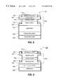
- FIG. 1illustrates a light-emitting device according to an embodiment of the present invention.
- FIG. 4illustrates a portion of a light-emitting device having three color pixels according to an embodiment of the present invention.
- FIG. 5illustrates a light-emitting device having at least one reflective layer according to another embodiment of the present layer.
- FIG. 7shows a light-emitting device having a mesa structure according to embodiment of the present invention.
- FIG. 1illustrates a light-emitting device according to an embodiment of the present invention.
- Light-emitting device 100includes contact layer 110 , active region 120 , substrate 130 , phosphor layer 140 and contact 150 .
- Active region 120can further include device layer 121 , active layer 122 , and device layer 123 .
- Active region 120can be any type of layer(s), which through the stimulated emission process, produces light having a particular band of wavelengths.
- This particular band of wavelengthscan be a subset of a large group of wavelengths that can be produced by a particular active layer.
- an active layer 122 constructed of at least Al x Ga 1-x N, where x is a value between 0 and 1can produce light having a band of wavelengths between approximately 300 nanometers and approximately 500 nanometers. This range of wavelengths (i.e., 300 nm to 500 nm) can be characterized as being between ultraviolet and blue.
- the group of possible wavelengths produced by active layer 122can be described as wavelengths producible by an active region constructed of at least Al x Ga 1-x N, where x is a value between 0 and 1.
- the active layer 122can be constructed of at least InGaN/Al x Ga 1-x N
- device layer 121can be a p-type AlGaN layer in contact with active layer 122
- device layer 123can be an n-type AlGaN layer disposed between and in contact with active layer 122 and substrate 130 .
- This type of active regionhas been described in previous publications.
- the active region 120can be activated by contact 110 and contact 150 where contact 150 has a ring shape around the device layer 123 .
- Substrate 130can be any type of substrate such as a sapphire substrate, silicon carbide or any other material that can be appropriately constructed adjacent to device layer 123 .
- Phosphor layer 140can be any appropriate type of coating having a matrix of wavelength-converting phosphors embedded within a binding material.
- phosphoris intended to mean any substance capable of luminescence while converting the wavelength(s) of incident light.
- Phosphorscan include, for example, polymers capable of luminescence. Table 1 illustrates a number of example coatings from which phosphor layer 140 can be constructed.
- contact 110is shown in FIG. 1 as extending over the entire surface of device layer 121 , the contact 110 can be configured in way that allows the appropriate excess carrier concentration within the active layer 133 via contacts 110 and 150 .
- contact 110can be configured with a ring shape.
- FIG. 2shows a light-emitting device according to another embodiment of the present invention.
- the light-emitting device 200 shown in FIG. 2is similar to light-emitting device 100 shown in FIG. 1 except that the substrate layer 130 of device 100 is not disposed between the active region and the phosphor layer, and the phosphor layer has been directly disposed in contact with one of the device layers. More specifically, light-emitting device 200 includes substrate 210 , contact 250 , active region 220 , phosphor layer 230 , and contact 240 . Active region 220 includes device layer 221 , active layer 222 and device layer 223 .
- the spontaneous emission within the active layere.g., active layer 122 shown in FIG. 1; active layer 222 shown in FIG. 2
- the spontaneous emission within the active layeris radiated isotropically and neglect radiation emitted in the direction opposite to the phosphor layer (e.g., phosphor layer 140 in FIG. 1; phosphor layer 230 in FIG. 2 ).
- n ais the refractive index of the device layer of the active region disposed between (but not necessarily in contact with) the active layer of the active region and the phosphor layer.
- n arelates to the device layer 123 ; as shown in FIG. 2, n a relates to device layer 223 .
- Equation (1)takes into account total internal reflection for excitation radiation propagating into the phosphor layer and neglects Fresnel reflection at the internal layer interfaces (e.g., the interface at substrate 130 and phosphor layer 140 as shown in FIG. 1 ).
- the coupling efficiency, ⁇ cfrom the active region to the phosphor layer increases with the phosphor layer refractive index, n c , increasing; however, the coupling efficiency for the interface between the phosphor layer and the medium exterior to phosphor layer (e.g., air) decreases as n c increases.
- Equation (2)Fresnel reflection at the interface of the phosphor layer and the medium exterior to phosphor layer, as well as total internal reflection at this interface is considered.
- the product of equations (1) and (2)produces (under the approximation of one light-path emitters) the upper limits for external efficiency of the light-emitting device, ⁇ e as a function n c .
- FIG. 3is a graph showing the external-efficiency upper limit versus the refractive index of a phosphor layer for a light-emitting device, according to an embodiment present.
- the external efficiency of the device, ⁇ eis maximum when n c equals n a . Consequently, Fresnel reflection at the interface of the device can be neglected at optimum conditions, e.g., in index-matched devices.
- Such considerationsare a reasonable basis for the selecting a phosphor layer having a particular refractive index when no intervening layers or materials are present between the active region and the phosphor layer (e.g., when a substrate is not disposed between the active region and the phosphor layer such as shown in FIG. 2 ).
- n arefractive index less than the active region refractive index
- the substrate 130when the substrate 130 is constructed of sapphire, its refractive index is approximately 1.75, which considerably less than the active region refractive index (e.g., n a ⁇ 2.25).
- a phosphor layer having a refractive index greater than the refractive index of the substratedoes not improve the external efficiency, ⁇ e , because the efficiency is limited by the interface of the active region and the substrate.
- increasing n c in the range of n c >n sdoes not improve the efficiency of the phosphor pumping (i.e., the coupling efficiency of active region to the phosphor layer).
- the refractive index of the phosphor layere.g., phosphor layer 230
- the refractive index of the device layer of the active region adjacent to the phosphor layere.g., device layer 223
- the refractive index of the substratee.g., substrate 130 and the refractive region of the phosphor layer (e.g., phosphor layer 140 ) should be substantially equal.
- the term“substantially equal” in this contextmeans as close as practical.
- the binding material and the phosphors of the phosphor layercan be selected so that the refractive index of the phosphor layer is close as practical to the refractive index of the device layer of the active region adjacent to the phosphor layer.
- the set of binding material and phosphors having a closer matching refractive index to the adjacent device layershould be selected.
- the set of binding material and phosphors having a closer matching refractive index to the substrateshould be selected.
- the concentration of phosphors within the phosphoris low, and therefore the refractive index of the phosphor layer does not substantially vary with the wavelengths associated with light.
- the phosphor concentrationis low when the refractive index of the phosphor layer is predominately defined by the refractive index of the binding material for the phosphor layer. Said another way, the phosphor concentration is low when phosphor layer refractive index at wavelengths associated with light produced by the active region is substantially the same as the phosphor layer refractive index at wavelengths associated with light wavelength-converted by the phosphor layer. In other words, when the phosphor layer has relatively low dispersion, the phosphor concentration is low.
- the phosphor layerhas a high phosphor concentration within the binding material.
- the phosphor layerlikely has strong absorption at wavelengths associated with light produced by the active region of the light-emitting device. Consequently, the phosphor layer refractive index, n ce , at wavelengths associated with light produced by the active region differs from the phosphor layer refractive index, n cr , at wavelengths associated with light wavelength-converted by the phosphor layer. This is the case, for example, with impurity ion-activated CdS and ZnS phosphors as well as with organic dye phosphors due to the strong Frank-Condon shift in organic materials.
- the binding material and the phosphorsshould be selected so that the phosphor layer refractive index, n ce , at wavelengths associated with light produced by the active region substantially equals the refractive index of the layer adjacent to and in contact with the phosphor layer (e.g., substrate 130 as shown in FIG. 1, or device layer 223 as shown in FIG. 2 ). If n ce ⁇ n a , no reflection losses occur and all the light produced in the active region propagating in the direction of phosphor layer could be converted to the wavelength-converted light.
- this binding material and the phosphorsalso should be selected so that the phosphor layer refractive index, n cr , at wavelengths associated with light wavelength-converted by the phosphor layer substantially equals the refractive index of the medium exterior to the phosphor layer.
- a mediumcan be, for example, an epoxy (having a refractive index of, for example, between 1.4 to 1.6), air, water, a vacuum, or other types of media having their own respective refractive index.
- the term“substantially equal” in this contextmeans as close as practical.
- the binding material and the phosphorscan be selected so that the refractive index of the phosphor layer, n ce , at wavelengths associated with light produced by the active region is close as practical to the refractive index of the substrate.
- the phosphor layer refractive index, n crat wavelengths associated with light wavelength-converted by the phosphor layer can be selected to be as close as practical to the refractive index of the medium exterior to the phosphor layer.
- the dispersion of refractive index of the phosphor layer, n ccan lead to the enhancement of the absolute value of the device external radiation efficiency.
- the ratio of the external efficiency for wavelength-converted radiation to the efficiency of an ultraviolet/blue light-emitting device not having phosphor coatingequals to 0.5 n a (n a +1) 2 /n cr (n cr +1) 2 .
- the factor 0.5is used because only half of the wavelength-converted radiation propagates in the direction of the emitting surface.
- the quantum efficiency of wavelength-converted radiationis expected to be 50% higher than efficiency of an ultraviolet/blue light-emitting device and its absolute value can be as high as 5% even in the framework of the one light-path model considered so far.
- FIG. 4illustrates a portion of a light-emitting device having three color pixels according to an embodiment of the present invention.
- Light-emitting device 400can include substrate 410 , device layer 420 , and pixels 430 , 440 and 450 .
- Each pixel 430 , 440 and 450can represent an individual color for a display application.
- pixel 430can produce light having wavelengths corresponding to red
- pixel 440can produce light having wavelengths corresponding the color green
- pixel 450can produce light having wavelengths corresponding to the color blue.
- FIG. 4illustrates a portion of a light-emitting device having three color pixels according to an embodiment of the present invention.
- Light-emitting device 400can include substrate 410 , device layer 420 , and pixels 430 , 440 and 450 .
- Each pixel 430 , 440 and 450can represent an individual color for a display application.
- pixel 430can produce light having wavelengths corresponding to red
- a light-emitting devicei.e., the portion having three pixels
- a light emitting devicecan include multiple pixels in, for example, a two-dimensional array.
- each pixelcan be individually addressable to provide a color display.
- Pixel 430further includes contact 431 , phosphor layer 432 , device layer 433 , active layer 434 and contact 435 .
- the active region 434can be defined as the device layer 433 , active layer 434 and the portion of device layer 420 that is adjacent and in contact with active layer 434 and contact 435 .
- Pixel 440further includes contact 441 , phosphor layer 442 , device layer 443 , active layer 444 and contact 445 .
- the active region 444can be defined as the device layer 443 , active layer 444 , and the portion of device layer 420 in contact with active layer 444 and contact 445 .
- pixel 450further includes contact 451 , phosphor layer 452 , device layer 453 , active layer 454 and contact 455 .
- the active region 454can be defined as the device layer 453 , active layer 454 , and the portion of device layer 420 in contact with active layer 445 and contact 455 .
- the phosphor layers 432 442 and 452can be selected so that each corresponding pixel 430 , 440 and 450 , respectively, emits light having wavelengths corresponding, in general red, green and blue, respectively. More specifically, pixel 450 can emit light having a band of wavelengths with a center wavelength between approximately 400 nanometers and approximately 550 nanometers. Pixel 440 can emit light having a band of wavelengths with a center wavelength between approximately 430 nanometers and approximately 650 nanometers. Pixel 430 can emit light having a band of wavelengths with a center wavelengths between approximately 550 nanometers and approximately 750 nanometers.
- the phosphor layer associated with the pixel that produces light having wavelengths between approximately 400 nanometers and approximately 550 nanometersneed not be present.
- the active layer of the pixel associated with blue wavelengthscan be selected so that the active layer produces light having predominately blue wavelengths.
- An associated phosphor layerneed not be necessarily present to perform wavelength conversion. Thus, the light produced in that active layer can just be directly transmitted for that associated pixel.
- the external efficiency of a light-emitting devicecan be considerably increased in the case of multi-path light processes.
- the light produced by an active layer propagating in a direction opposite from the wavelength-converting phosphor layercan be reflected back, thereby doubling the pumping efficiency of the active layer into the phosphor layer.
- a reflective layerfor example, can be optically coupled to the active region.
- the term“optically coupled”is used here to mean operatively associated such that light emitted from the active region is reflected by the reflective layer.
- the reflective layermay be adjacent to and in contact with the active layer, or an intervening layer (e.g., a substrate) may be disposed between the reflective layer and the active layer.
- wavelength selective reflective layerthat is wavelength selective can be disposed between the active region and the phosphor layer.
- a wavelength-selective reflective layerwould allow light produced within the active region to be transmitted and allow light produced with the phosphor layer to be reflective back out towards the emitting surface of the light-emitting device.
- wavelength selective reflecting GaN/AlGaN filterscan be grown on a sapphire substrate.
- FIG. 5illustrates a light-emitting device having at least one reflective layer according to another embodiment of the present layer.
- Light-emitting device 500includes substrate 510 , contact 560 , reflective layer 520 , active region 530 , reflective layer 540 , phosphor layer 550 and contact 570 .
- Active region 530includes device layer 531 , active layer 532 and device layer 533 .
- reflective layer 520is configured to reflect light having the band of wavelengths produced by active layer 532 of active region 530 as well as phosphor-converted light having a second band of wavelengths produced in phosphor layer 550 .
- active layer 532can produce light having a first band of wavelengths (e.g., predominately blue colored light) that is propagated towards reflective layer 520 .
- lightcan be wavelength-converted by phosphor layer 550 and propagate towards reflective layer 520 .
- reflective layer 520can reflect both light having the first band of wavelengths and light having the second band of wavelengths (i.e., light wavelength-converted by phosphor layer 500 ).
- Reflective layer 540can be a wavelength selective reflective layer.
- reflective layer 540can be configured so that light having the first band of wavelengths (i.e., light produced by active layer 532 ) is transmitted while light having the second band of wavelengths (i.e., wavelength-converted light) produced in phosphor layer 550 is reflected at the boundary between reflective layer 540 and phosphor layer 550 .
- this lightis then allowed to exit light-emitting device 500 more efficiently and does not needlessly propagate through the other layers of light-emitting device 500 (e.g., device layer 533 , active layer 532 , device layer 531 ).
- only one reflective layercan be present.
- the reflective layer between the contact and the device layercan be present without a reflective layer between device layer and phosphor layer being present.
- the oppositemay be true; in other words, the reflective layer between the device layer and phosphor layer may be present, while the reflective layer between the contact and the device layer are not present.
- FIG. 6illustrates a light-emitting device having a reflective layer according to yet another embodiment of the present invention.
- Light-emitting device 600includes phosphor layer 610 , contact 620 , active region 630 , contact 640 , reflective layer 650 and substrate 660 .
- Active region 630includes device layer 631 , active layer 632 and device layer 633 .
- Reflective layer 650is configured to reflect light having the first band of wavelengths (e.g., light produced by active layer 632 of active region 630 ) and light having a second band of wavelengths (e.g., light produced through wavelength-conversion by phosphor layer 610 ).
- light produced by active layer 632can propagate in the direction of reflective layer 650 and light produced through wavelength-conversion in phosphor layer 610 can also be propagated in the direction of reflective layer 650 .
- Light having either of these bands of wavelengthsare reflected by reflective layer 650 are redirected towards phosphor layer 610 where the light can ultimately exit light emitting 600 .
- a wavelength-selective reflective layercan be disposed between device layer 631 and phosphor layer 620 .
- Such a wavelength-selective reflective layercan be configured so that light having a first band of wavelengths (i.e., light produced by active layer 632 ) is transmitted while light having a second band of wavelengths (i.e., wavelength-converted light) produced in phosphor layer 620 is reflected at the boundary between the wavelength-selective reflective layer and phosphor layer 620 .
- the concept of the reflective layer shown in FIG. 6can also be applicable to other embodiments of the present invention such as, for example, light-emitting device 400 shown in FIG. 4 .
- a reflective layercan be added between device layer 420 and substrate 410 .
- the reflective layerreflects all wavelengths for the light produced in active layers 434 , 444 and 454 , as well as wavelength-converted light produced in phosphor layers 432 , 442 and 452 .
- such a reflective layercan reflect light having, for example, predominately ultraviolet to blue wavelengths produced in the active layers and can also reflect wavelength-converted light having predominately blue color associated with pixel 450 , a green color produced by pixel 440 , and a red color produced by pixel 430 .
- a wavelength-selective reflective layercan be disposed between phosphor layer 432 and device layer 433 .
- the external efficiency of a light-emitting device described abovecan be further improved by collecting light emitted in the directions close to parallel to the plane of device layers (i.e., close to parallel to the direction of propagation out of the light-emitting device).
- GaN device layers of the active regionform a waveguide because their effective refractive index is higher than that of the substrate.
- Inclined sidewalls of the devicee.g., a mesa-like structure
- the light-emitting device described above that incorporates the reflective layer and a mesa-like structurecan potentially achieve external efficiency for the device as high as 20-30% throughout all of the visible spectrum.
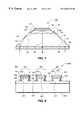
- FIG. 7shows a light-emitting device having a mesa structure according to embodiment of the present invention.
- Light-emitting device 700includes a contact 710 , active region 720 , contact 730 , substrate 740 and phosphor layer 750 .
- Active region 720includes device layer 721 , active layer 722 , and device layer 723 .
- Substrate 740includes a first side 741 , a second side 742 and side wall 743 .
- a set of rays showing light propagating through light-emitting device 700are rays 760 , 770 and 780 .
- Substrate 740forms a mesa structure. More specifically, substrate 740 has a sidewall 740 that forms an incline angle, 0 , which is non-normal to the surface of second side 742 of substrate 740 . Said another way, because the first side 741 of substrate 740 has a smaller area than the second side 742 of substrate 740 , the sidewall 743 formed by substrate 740 is at an incline.
- a mediumis disposed exterior to and in contact with the sidewall 743 of substrate 740 .
- This external mediumhas its own refractive index and is label in FIG. 7 as 790 .
- the particular incline angle appropriate for sidewall 743depends on the refractive index of the substrate and the refractive index of the exterior medium 790 . More particularly, the refractive index of exterior medium 790 and the refractive index of substrate 740 are factors because light emitted within substrate 740 interacts at the sidewall 743 according to Snell's law.
- the exterior medium 790can be, for example, an epoxy (having a refractive index of, for example, between 1.4 to 1.6), air, a vacuum, or other types of media having their own respective refractive index.
- the refractive index of the substrate 740can be, for example, between 1.75 and 2.0.
- the particular refractive index of substrate 740 and the refractive index of the exterior medium 790can define how light propagating within substrate 740 can be reflected according to totally internal reflection.
- the following relationshipcan define an optimal incline angle: ⁇ 90° ⁇ arcsin (n 2 /n 1 ), where n 1 is the refractive index of the substrate 740 and n 2 is the refractive index of the exterior medium 790 .
- this relationshipcan be generalized for other layers of the device by equating n 2 with the refractive index of that layer of the light-emitting device and by equating n 1 with the medium exterior to that layer.
- n 2the refractive index of that layer of the light-emitting device
- n 1the medium exterior to that layer.
- the sidewall of substratecan be inclined, so too can the corresponding sidewalls of device layers 721 , active layer 722 and device layer 723 can be inclined.
- the incline angle of the sidewalls for layers 721 , 722 and 723can be the same or can be different from the incline angle of the sidewall 743 for substrate 740 .
- at least one side wall from the first device layer, the active layer, the second device layer and/or the substratecan be inclined to direct more light towards the emitting surface.
- the substrateis a sapphire substrate having a refractive index of approximately 1.75 and the layers of the active region have refractive indices of approximately 2.0, the incline angle, ⁇ , of the sidewalls for the light-emitting device will between approximately 40 degrees and 60 degrees.
- FIG. 8illustrates a light emitting device having multiple pixels where each pixel have a mesa-like structure according to the embodiment of the present invention.
- Light-emitting device 800includes substrate 810 , device layer 820 , and pixels 830 , 840 and 850 .
- Pixel 830includes contact 831 , phosphor layer 832 , device layer 833 , active layer 834 and contact 835 .
- pixel 840includes contact 841 , phosphor layer 842 , device layer 843 , active layer 844 and contact 845 .
- pixel 850includes contact 851 , phosphor layer 852 , device layer 853 , active layer 854 , and contact 855 .
- a given pixel or multiple pixels of light-emitting device 800 showed in FIG. 8can have a mesa structure.
- the following discussionrelate to pixel 830 , although an analogous structure can also be implemented for pixels 840 and 850 , as well as any other pixels (not shown) of a two-dimensional pixel array for light-emitting device 800 .
- Device layer 833which is disposed between and in contact with phosphor layer 832 and active layer 834 , has a first side that is adjacent to active layer 834 and a second side that is adjacent to phosphor layer 832 and a sidewall 836 .
- a medium exterior to sidewall 836is labeled in FIG. 8 as 860 and has its own refractive index.
- Sidewall 836can be inclined at angle, ⁇ .
- This incline angle, ⁇should be less than 90 degrees and as discussed above can vary between 40 and 60 degrees according to the above-described relationship between ⁇ , the refractive index of exterior medium and the refractive index of the device layer 833 .
- the analogous sidewalls of active layer 834 and the portion of device layer 820 adjacent to active layer 834can also be inclined at an angle, such as, for example, the incline angle, ⁇ .
Landscapes
- Led Device Packages (AREA)
- Led Devices (AREA)
Abstract
Description
| Wavelength | |||
| of max. | Photon conversion | ||
| emission | efficiency at wavelength of excitation: | ||
| Coating: | (nm) | 254 nm | 312 nm | 365 nm | 405 nm | 436 nm |
| PPO in 2045 | 400 | 0.49 | 0.80 | — | — | |
| Bis-MSB in 2045 | 450 | 0.74 | 0.93 | 0.94 | — | — |
| “Blue Coating” (p-terph. + | 430 | 0.93 | 0.92 | 0.95 | — | — |
| PPO + Bis-MSB in 2045) | ||||||
| Hostasol | 510 | 0.12 | 0.21 | 0.10 | 0.18 | 0.17 |
| Laser dye #481 in 2045 | 490 | 0.75 | 0.39 | 0.83 | 0.91 | 0.90 |
| Laser dye #495 in 2045 | 520 | 0.21 | 0.10 | 0.28 | 0.34 | 0.36 |
| “Green Coating” (#481 + | 510 | 0.80 | 0.42 | 0.85 | 0.95 | 0.95 |
| Hostasol 8G in 2045) | ||||||
| BBQ in 2045 | 495 | 0.78 | 0.62 | 0.83 | 0.87 | 0.82 |
| “Red Coating” (#481 + | 610 | 0.55 | 0.38 | 0.76 | 0.90 | 0.93 |
| Hostasol 8G & Hostasol GG in | ||||||
| 2045) | ||||||


Claims (34)
Priority Applications (9)
| Application Number | Priority Date | Filing Date | Title |
|---|---|---|---|
| US09/421,584US6404125B1 (en) | 1998-10-21 | 1999-10-20 | Method and apparatus for performing wavelength-conversion using phosphors with light emitting diodes |
| JP2000577717AJP2002528898A (en) | 1998-10-21 | 1999-10-21 | Method and apparatus for performing wavelength conversion using phosphor having light emitting diode |
| EP99955154AEP1166368A4 (en) | 1998-10-21 | 1999-10-21 | METHOD AND DEVICE FOR CONVERTING THE WAVELENGTH WITH THE USE OF A LUMINAIRE WITH LIGHT-EMITTING DIODES |
| CA002346042ACA2346042C (en) | 1998-10-21 | 1999-10-21 | A method and apparatus for performing wavelength-conversion using phosphors with light emitting diodes |
| IL14239499AIL142394A0 (en) | 1998-10-21 | 1999-10-21 | A method and apparatus for performing wavelength-conversion using phosphors with light emitting diodes |
| PCT/US1999/024911WO2000024064A1 (en) | 1998-10-21 | 1999-10-21 | A method and apparatus for performing wavelength-conversion using phosphors with light emitting diodes |
| KR1020017004820AKR100664352B1 (en) | 1998-10-21 | 1999-10-21 | Method and apparatus having light-emitting diode and performing wavelength-conversion using phosphor |
| AU11326/00AAU1132600A (en) | 1998-10-21 | 1999-10-21 | A method and apparatus for performing wavelength-conversion using phosphors withlight emitting diodes |
| CN99812442ACN1324498A (en) | 1998-10-21 | 1999-10-21 | Method and apparatus for performing wavelength-cnversion using phosphors with light emitting diodes |
Applications Claiming Priority (2)
| Application Number | Priority Date | Filing Date | Title |
|---|---|---|---|
| US10505698P | 1998-10-21 | 1998-10-21 | |
| US09/421,584US6404125B1 (en) | 1998-10-21 | 1999-10-20 | Method and apparatus for performing wavelength-conversion using phosphors with light emitting diodes |
Publications (1)
| Publication Number | Publication Date |
|---|---|
| US6404125B1true US6404125B1 (en) | 2002-06-11 |
Family
ID=26802208
Family Applications (1)
| Application Number | Title | Priority Date | Filing Date |
|---|---|---|---|
| US09/421,584Expired - LifetimeUS6404125B1 (en) | 1998-10-21 | 1999-10-20 | Method and apparatus for performing wavelength-conversion using phosphors with light emitting diodes |
Country Status (9)
| Country | Link |
|---|---|
| US (1) | US6404125B1 (en) |
| EP (1) | EP1166368A4 (en) |
| JP (1) | JP2002528898A (en) |
| KR (1) | KR100664352B1 (en) |
| CN (1) | CN1324498A (en) |
| AU (1) | AU1132600A (en) |
| CA (1) | CA2346042C (en) |
| IL (1) | IL142394A0 (en) |
| WO (1) | WO2000024064A1 (en) |
Cited By (88)
| Publication number | Priority date | Publication date | Assignee | Title |
|---|---|---|---|---|
| US6504181B2 (en)* | 1999-12-21 | 2003-01-07 | Kabushiki Kaisha Toshiba | Semiconductor light emitting element and manufacturing method thereof |
| US6639350B1 (en)* | 1998-02-05 | 2003-10-28 | Zumiobel Staff Gmbh | Illumination arrangement |
| US6650044B1 (en)* | 2000-10-13 | 2003-11-18 | Lumileds Lighting U.S., Llc | Stenciling phosphor layers on light emitting diodes |
| US20040051947A1 (en)* | 2001-09-25 | 2004-03-18 | Masaki Kagawa | Polarizing beam splitter and polarizer using this |
| US20040056260A1 (en)* | 2002-09-19 | 2004-03-25 | Slater David B. | Phosphor-coated light emitting diodes including tapered sidewalls, and fabrication methods therefor |
| US20040116033A1 (en)* | 2003-01-27 | 2004-06-17 | 3M Innovative Properties Company | Methods of making phosphor based light sources having an interference reflector |
| US20040135502A1 (en)* | 2002-12-25 | 2004-07-15 | Makoto Kobayashi | Color-conversion light-emitting device, method for manufacturing the same, and display using the same |
| US20040145289A1 (en)* | 2003-01-27 | 2004-07-29 | 3M Innovative Properties Company | Phosphor based light sources having a non-planar short pass reflector and method of making |
| US20040145913A1 (en)* | 2003-01-27 | 2004-07-29 | 3M Innovative Properties Company | Phosphor based light sources having a polymeric long pass reflector |
| US20040145895A1 (en)* | 2003-01-27 | 2004-07-29 | 3M Innovative Properties Company | Phosphor based light sources having a non-planar long pass reflector and method of making |
| US20040145312A1 (en)* | 2003-01-27 | 2004-07-29 | 3M Innovative Properties Company | Phosphor based light source having a flexible short pass reflector |
| US20040150997A1 (en)* | 2003-01-27 | 2004-08-05 | 3M Innovative Properties Company | Phosphor based light sources having a reflective polarizer |
| US20040159900A1 (en)* | 2003-01-27 | 2004-08-19 | 3M Innovative Properties Company | Phosphor based light sources having front illumination |
| US20040257797A1 (en)* | 2003-06-18 | 2004-12-23 | Yoshinobu Suehiro | Light emitting device |
| US20050051789A1 (en)* | 2003-09-09 | 2005-03-10 | Negley Gerald H. | Solid metal block mounting substrates for semiconductor light emitting devices, and oxidizing methods for fabricating same |
| US20050062140A1 (en)* | 2003-09-18 | 2005-03-24 | Cree, Inc. | Molded chip fabrication method and apparatus |
| WO2005048364A1 (en)* | 2003-11-12 | 2005-05-26 | Cree, Inc. | Light emitting devices with self aligned ohmic contact and methods of fabricating same |
| KR100499129B1 (en)* | 2002-09-02 | 2005-07-04 | 삼성전기주식회사 | Light emitting laser diode and fabricatin method thereof |
| US20060005763A1 (en)* | 2001-12-24 | 2006-01-12 | Crystal Is, Inc. | Method and apparatus for producing large, single-crystals of aluminum nitride |
| US20060038195A1 (en)* | 2002-12-13 | 2006-02-23 | Shyi-Ming Pan | Light-emitting diode and the manufacturing method of the same |
| US7029935B2 (en) | 2003-09-09 | 2006-04-18 | Cree, Inc. | Transmissive optical elements including transparent plastic shell having a phosphor dispersed therein, and methods of fabricating same |
| US20060097385A1 (en)* | 2004-10-25 | 2006-05-11 | Negley Gerald H | Solid metal block semiconductor light emitting device mounting substrates and packages including cavities and heat sinks, and methods of packaging same |
| US20060139945A1 (en)* | 2004-12-23 | 2006-06-29 | Negley Gerald H | Light emitting diode arrays for direct backlighting of liquid crystal displays |
| US20060152651A1 (en)* | 2005-01-12 | 2006-07-13 | Negley Gerald H | Solid colloidal dispersions for backlighting of liquid crystal displays |
| US20060175621A1 (en)* | 2001-12-28 | 2006-08-10 | Sanken Electric Co., Ltd. | Semiconductor light-emitting device light-emitting display method for manufacturing semiconductor light-emitting device and method for manufacturing light-emitting display |
| US7091653B2 (en) | 2003-01-27 | 2006-08-15 | 3M Innovative Properties Company | Phosphor based light sources having a non-planar long pass reflector |
| USD536308S1 (en)* | 2004-10-19 | 2007-02-06 | Rohm Co., Ltd. | Light emitting diode |
| USD539240S1 (en)* | 2004-10-19 | 2007-03-27 | Rohm Co., Ltd. | Light emitting diode |
| WO2007052777A1 (en)* | 2005-11-04 | 2007-05-10 | Matsushita Electric Industrial Co., Ltd. | Light-emitting module, and display unit and lighting unit using the same |
| US20070114559A1 (en)* | 2005-11-23 | 2007-05-24 | Visteon Global Technologies, Inc. | Light emitting diode device having a shield and/or filter |
| US20070131160A1 (en)* | 2005-12-02 | 2007-06-14 | Slack Glen A | Doped aluminum nitride crystals and methods of making them |
| US20070170447A1 (en)* | 2006-01-20 | 2007-07-26 | Led Lighting Fixtures, Inc. | Shifting spectral content in solid state light emitters by spatially separating lumiphor films |
| US20070170445A1 (en)* | 2004-08-24 | 2007-07-26 | Kabushiki Kaisha Toshiba | Semiconductor light-emitting device |
| US20070182299A1 (en)* | 2003-01-27 | 2007-08-09 | 3M Innovative Properties Company | Phosphor based light source component |
| US20070224716A1 (en)* | 2004-09-21 | 2007-09-27 | Cree, Inc. | Methods of coating semiconductor light emitting elements by evaporating solvent from a suspension |
| US20070228935A1 (en)* | 2006-03-22 | 2007-10-04 | Kim Bum J | White light emitting device |
| US20070228387A1 (en)* | 2006-04-04 | 2007-10-04 | Gerald Negley | Uniform emission LED package |
| US20070243653A1 (en)* | 2006-03-30 | 2007-10-18 | Crystal Is, Inc. | Methods for controllable doping of aluminum nitride bulk crystals |
| US20070248132A1 (en)* | 2004-08-31 | 2007-10-25 | Akihiko Kikuchi | Light Emitting Element and Method of Manufacturing the Same |
| US20070274080A1 (en)* | 2006-05-23 | 2007-11-29 | Led Lighting Fixtures, Inc. | Lighting device |
| US20080079017A1 (en)* | 2006-07-31 | 2008-04-03 | Cree, Inc. | Method of uniform phosphor chip coating and led package fabricated using method |
| US20080142816A1 (en)* | 2006-12-15 | 2008-06-19 | Philips Lumileds Lighting Company Llc | Tunable White Point Light Source Using a Wavelength Converting Element |
| US20080170396A1 (en)* | 2006-11-09 | 2008-07-17 | Cree, Inc. | LED array and method for fabricating same |
| US20080173884A1 (en)* | 2007-01-22 | 2008-07-24 | Cree, Inc. | Wafer level phosphor coating method and devices fabricated utilizing method |
| US20080179611A1 (en)* | 2007-01-22 | 2008-07-31 | Cree, Inc. | Wafer level phosphor coating method and devices fabricated utilizing method |
| US20080187016A1 (en)* | 2007-01-26 | 2008-08-07 | Schowalter Leo J | Thick Pseudomorphic Nitride Epitaxial Layers |
| US20080284329A1 (en)* | 2004-06-18 | 2008-11-20 | Koninklijke Philips Electronics, N.V. | Led with Improve Light Emittance Profile |
| US20090014736A1 (en)* | 2007-07-11 | 2009-01-15 | Cree, Inc. | Coating method utilizing phosphor containment structure and devices fabricated using same |
| US20090040745A1 (en)* | 2007-05-08 | 2009-02-12 | Luminus Devices, Inc. | Light emitting devices including wavelength converting material |
| US20090050050A1 (en)* | 2007-05-24 | 2009-02-26 | Crystal Is, Inc. | Deep-eutectic melt growth of nitride crystals |
| US20090057690A1 (en)* | 2007-01-22 | 2009-03-05 | Cree, Inc. | Wafer level phosphor coating technique for warm light emitting diodes |
| US20090153022A1 (en)* | 2007-12-14 | 2009-06-18 | Hussell Christopher P | Phosphor distribution in LED lamps using centrifugal force |
| US7614759B2 (en) | 2005-12-22 | 2009-11-10 | Cree Led Lighting Solutions, Inc. | Lighting device |
| US20090309114A1 (en)* | 2008-01-16 | 2009-12-17 | Luminus Devices, Inc. | Wavelength converting light-emitting devices and methods of making the same |
| US7638346B2 (en) | 2001-12-24 | 2009-12-29 | Crystal Is, Inc. | Nitride semiconductor heterostructures and related methods |
| US20100033947A1 (en)* | 2008-08-06 | 2010-02-11 | Kismart Corp. | Enhanced Wavelength-Converting Structure |
| US20100151612A1 (en)* | 2007-03-16 | 2010-06-17 | Toyoda Gosei Co., Ltd. | Group III-V semiconductor device and method for producing the same |
| US20100264460A1 (en)* | 2007-01-26 | 2010-10-21 | Grandusky James R | Thick pseudomorphic nitride epitaxial layers |
| US20100295073A1 (en)* | 2007-06-26 | 2010-11-25 | Osram Opto Semiconductors Gmbh | Optoelectronic Semiconductor Chip |
| US20100314551A1 (en)* | 2009-06-11 | 2010-12-16 | Bettles Timothy J | In-line Fluid Treatment by UV Radiation |
| US20110008621A1 (en)* | 2006-03-30 | 2011-01-13 | Schujman Sandra B | Aluminum nitride bulk crystals having high transparency to ultraviolet light and methods of forming them |
| US8240875B2 (en) | 2008-06-25 | 2012-08-14 | Cree, Inc. | Solid state linear array modules for general illumination |
| US8323406B2 (en) | 2007-01-17 | 2012-12-04 | Crystal Is, Inc. | Defect reduction in seeded aluminum nitride crystal growth |
| US8337071B2 (en) | 2005-12-21 | 2012-12-25 | Cree, Inc. | Lighting device |
| US8349077B2 (en) | 2005-11-28 | 2013-01-08 | Crystal Is, Inc. | Large aluminum nitride crystals with reduced defects and methods of making them |
| US8441179B2 (en) | 2006-01-20 | 2013-05-14 | Cree, Inc. | Lighting devices having remote lumiphors that are excited by lumiphor-converted semiconductor excitation sources |
| US8466611B2 (en) | 2009-12-14 | 2013-06-18 | Cree, Inc. | Lighting device with shaped remote phosphor |
| US20130175566A1 (en)* | 2011-07-14 | 2013-07-11 | Panasonic Corporation | Nitride-based semiconductor light-emitting element |
| US8637883B2 (en) | 2008-03-19 | 2014-01-28 | Cree, Inc. | Low index spacer layer in LED devices |
| US8772817B2 (en) | 2010-12-22 | 2014-07-08 | Cree, Inc. | Electronic device submounts including substrates with thermally conductive vias |
| US8962359B2 (en) | 2011-07-19 | 2015-02-24 | Crystal Is, Inc. | Photon extraction from nitride ultraviolet light-emitting devices |
| US9028612B2 (en) | 2010-06-30 | 2015-05-12 | Crystal Is, Inc. | Growth of large aluminum nitride single crystals with thermal-gradient control |
| US9041285B2 (en) | 2007-12-14 | 2015-05-26 | Cree, Inc. | Phosphor distribution in LED lamps using centrifugal force |
| US9166126B2 (en) | 2011-01-31 | 2015-10-20 | Cree, Inc. | Conformally coated light emitting devices and methods for providing the same |
| US20160049444A1 (en)* | 2009-02-24 | 2016-02-18 | Epistar Corporation | Array-type light-emitting device and apparatus thereof |
| US9299880B2 (en) | 2013-03-15 | 2016-03-29 | Crystal Is, Inc. | Pseudomorphic electronic and optoelectronic devices having planar contacts |
| US20160155901A1 (en)* | 2013-07-18 | 2016-06-02 | Koninklijke Philips N.V. | Highly reflective flip chip led die |
| US9447521B2 (en) | 2001-12-24 | 2016-09-20 | Crystal Is, Inc. | Method and apparatus for producing large, single-crystals of aluminum nitride |
| US9608166B2 (en) | 2003-08-14 | 2017-03-28 | Cree, Inc. | Localized annealing of metal-silicon carbide ohmic contacts and devices so formed |
| US9771666B2 (en) | 2007-01-17 | 2017-09-26 | Crystal Is, Inc. | Defect reduction in seeded aluminum nitride crystal growth |
| US9841175B2 (en) | 2012-05-04 | 2017-12-12 | GE Lighting Solutions, LLC | Optics system for solid state lighting apparatus |
| US20180074372A1 (en)* | 2016-09-12 | 2018-03-15 | Seoul Semiconductor Co., Ltd. | Display apparatus |
| US9951938B2 (en) | 2009-10-02 | 2018-04-24 | GE Lighting Solutions, LLC | LED lamp |
| US10340424B2 (en) | 2002-08-30 | 2019-07-02 | GE Lighting Solutions, LLC | Light emitting diode component |
| US10546846B2 (en) | 2010-07-23 | 2020-01-28 | Cree, Inc. | Light transmission control for masking appearance of solid state light sources |
| WO2020219594A1 (en)* | 2019-04-22 | 2020-10-29 | Crystal Is, Inc. | Fluid treatment reactor |
| TWI725564B (en)* | 2019-09-30 | 2021-04-21 | 台達電子工業股份有限公司 | Wavelength conversion device |
| US12199213B2 (en) | 2018-03-02 | 2025-01-14 | Sharp Kabushiki Kaisha | Image display device |
Families Citing this family (35)
| Publication number | Priority date | Publication date | Assignee | Title |
|---|---|---|---|---|
| WO2002029906A2 (en)* | 2000-10-04 | 2002-04-11 | Lighthouse Technologies Ltd. | Led with embedded conversion layer |
| US6660928B1 (en) | 2002-04-02 | 2003-12-09 | Essential Research, Inc. | Multi-junction photovoltaic cell |
| JP4143732B2 (en)* | 2002-10-16 | 2008-09-03 | スタンレー電気株式会社 | In-vehicle wavelength converter |
| JP2005072323A (en)* | 2003-08-26 | 2005-03-17 | Oki Data Corp | Semiconductor device |
| KR100613273B1 (en)* | 2003-12-30 | 2006-08-18 | 주식회사 이츠웰 | Light emitting diodes and manufacturing method thereof |
| US7837348B2 (en) | 2004-05-05 | 2010-11-23 | Rensselaer Polytechnic Institute | Lighting system using multiple colored light emitting sources and diffuser element |
| US20060091411A1 (en) | 2004-10-29 | 2006-05-04 | Ouderkirk Andrew J | High brightness LED package |
| US7404652B2 (en)* | 2004-12-15 | 2008-07-29 | Avago Technologies Ecbu Ip Pte Ltd | Light-emitting diode flash module with enhanced spectral emission |
| JP4777757B2 (en)* | 2005-12-01 | 2011-09-21 | スタンレー電気株式会社 | Semiconductor light emitting device and manufacturing method thereof |
| US7889421B2 (en) | 2006-11-17 | 2011-02-15 | Rensselaer Polytechnic Institute | High-power white LEDs and manufacturing method thereof |
| US8157730B2 (en) | 2006-12-19 | 2012-04-17 | Valencell, Inc. | Physiological and environmental monitoring systems and methods |
| US8652040B2 (en) | 2006-12-19 | 2014-02-18 | Valencell, Inc. | Telemetric apparatus for health and environmental monitoring |
| US8320982B2 (en) | 2006-12-27 | 2012-11-27 | Valencell, Inc. | Multi-wavelength optical devices and methods of using same |
| US8251903B2 (en) | 2007-10-25 | 2012-08-28 | Valencell, Inc. | Noninvasive physiological analysis using excitation-sensor modules and related devices and methods |
| WO2009085594A2 (en)* | 2007-12-28 | 2009-07-09 | 3M Innovative Properties Company | Down-converted light source with uniform wavelength emission |
| DE102008012407A1 (en)* | 2008-01-31 | 2009-08-06 | Osram Opto Semiconductors Gmbh | Radiation-emitting device |
| US9750462B2 (en) | 2009-02-25 | 2017-09-05 | Valencell, Inc. | Monitoring apparatus and methods for measuring physiological and/or environmental conditions |
| US8788002B2 (en) | 2009-02-25 | 2014-07-22 | Valencell, Inc. | Light-guiding devices and monitoring devices incorporating same |
| EP3127476A1 (en) | 2009-02-25 | 2017-02-08 | Valencell, Inc. | Light-guiding devices and monitoring devices incorporating same |
| US8218133B2 (en)* | 2010-09-16 | 2012-07-10 | Sondex Limited | Refractive index tool and method |
| US8888701B2 (en) | 2011-01-27 | 2014-11-18 | Valencell, Inc. | Apparatus and methods for monitoring physiological data during environmental interference |
| WO2013016007A2 (en) | 2011-07-25 | 2013-01-31 | Valencell, Inc. | Apparatus and methods for estimating time-state physiological parameters |
| WO2013019494A2 (en) | 2011-08-02 | 2013-02-07 | Valencell, Inc. | Systems and methods for variable filter adjustment by heart rate metric feedback |
| DE102012102301B4 (en) | 2012-03-19 | 2021-06-17 | OSRAM Opto Semiconductors Gesellschaft mit beschränkter Haftung | Optoelectronic semiconductor chip and headlight with such a semiconductor chip |
| TW201405864A (en)* | 2012-07-30 | 2014-02-01 | Lextar Electronics Corp | Light-emitting diode having undercut structure and manufacturing method thereof |
| CN110013239A (en) | 2013-01-28 | 2019-07-16 | 瓦伦赛尔公司 | Physiological monitoring device with the sensing element disengaged with body kinematics |
| JP6713720B2 (en)* | 2013-08-30 | 2020-06-24 | エルジー イノテック カンパニー リミテッド | Light emitting device package and vehicle lighting device including the same |
| JP6216209B2 (en)* | 2013-10-24 | 2017-10-18 | スタンレー電気株式会社 | Semiconductor light emitting device |
| US9538921B2 (en) | 2014-07-30 | 2017-01-10 | Valencell, Inc. | Physiological monitoring devices with adjustable signal analysis and interrogation power and monitoring methods using same |
| EP3199100A1 (en) | 2014-08-06 | 2017-08-02 | Valencell, Inc. | Earbud with a physiological information sensor module |
| US9794653B2 (en) | 2014-09-27 | 2017-10-17 | Valencell, Inc. | Methods and apparatus for improving signal quality in wearable biometric monitoring devices |
| JP6397298B2 (en)* | 2014-10-06 | 2018-09-26 | 日本放送協会 | Light emitting element |
| US10610158B2 (en) | 2015-10-23 | 2020-04-07 | Valencell, Inc. | Physiological monitoring devices and methods that identify subject activity type |
| US10945618B2 (en) | 2015-10-23 | 2021-03-16 | Valencell, Inc. | Physiological monitoring devices and methods for noise reduction in physiological signals based on subject activity type |
| WO2018009736A1 (en) | 2016-07-08 | 2018-01-11 | Valencell, Inc. | Motion-dependent averaging for physiological metric estimating systems and methods |
Citations (17)
| Publication number | Priority date | Publication date | Assignee | Title |
|---|---|---|---|---|
| US5399499A (en) | 1994-05-13 | 1995-03-21 | Eastman Kodak Company | Method of using multiwavelength upconversion for sample element interrogation in medical diagnostic equipment |
| US5684360A (en) | 1995-07-10 | 1997-11-04 | Intevac, Inc. | Electron sources utilizing negative electron affinity photocathodes with ultra-small emission areas |
| US5813752A (en) | 1997-05-27 | 1998-09-29 | Philips Electronics North America Corporation | UV/blue LED-phosphor device with short wave pass, long wave pass band pass and peroit filters |
| US5813753A (en) | 1997-05-27 | 1998-09-29 | Philips Electronics North America Corporation | UV/blue led-phosphor device with efficient conversion of UV/blues light to visible light |
| US5835119A (en) | 1995-10-31 | 1998-11-10 | Hewlett- Packard Company | Face emitting electroluminescent exposure array |
| US5847507A (en) | 1997-07-14 | 1998-12-08 | Hewlett-Packard Company | Fluorescent dye added to epoxy of light emitting diode lens |
| US5851063A (en) | 1996-10-28 | 1998-12-22 | General Electric Company | Light-emitting diode white light source |
| US5886401A (en) | 1997-09-02 | 1999-03-23 | General Electric Company | Structure and fabrication method for interconnecting light emitting diodes with metallization extending through vias in a polymer film overlying the light emitting diodes |
| US5895932A (en) | 1997-01-24 | 1999-04-20 | International Business Machines Corporation | Hybrid organic-inorganic semiconductor light emitting diodes |
| US5898185A (en) | 1997-01-24 | 1999-04-27 | International Business Machines Corporation | Hybrid organic-inorganic semiconductor light emitting diodes |
| EP0936682A1 (en) | 1996-07-29 | 1999-08-18 | Nichia Chemical Industries, Ltd. | Light emitting device and display device |
| US5952681A (en) | 1997-11-24 | 1999-09-14 | Chen; Hsing | Light emitting diode emitting red, green and blue light |
| US5959316A (en) | 1998-09-01 | 1999-09-28 | Hewlett-Packard Company | Multiple encapsulation of phosphor-LED devices |
| US5959307A (en) | 1995-11-06 | 1999-09-28 | Nichia Chemical Industries Ltd. | Nitride semiconductor device |
| US5962843A (en) | 1997-07-17 | 1999-10-05 | Sinor; Timothy Wayne | Night vision having an image intensifier tube, improved transmission mode photocathode for such a device, and method of making |
| US5982092A (en) | 1997-10-06 | 1999-11-09 | Chen; Hsing | Light Emitting Diode planar light source with blue light or ultraviolet ray-emitting luminescent crystal with optional UV filter |
| US5994722A (en) | 1996-10-31 | 1999-11-30 | Siemens Aktiengesellschaft | Image display device that emits multicolored light |
Family Cites Families (3)
| Publication number | Priority date | Publication date | Assignee | Title |
|---|---|---|---|---|
| JPH09153645A (en)* | 1995-11-30 | 1997-06-10 | Toyoda Gosei Co Ltd | Group III nitride semiconductor light emitting device |
| EP0856202A2 (en)* | 1996-06-11 | 1998-08-05 | Koninklijke Philips Electronics N.V. | Visible light emitting devices including uv-light emitting diode and uv-excitable, visible light emitting phosphor, and method of producing such devices |
| JPH10209505A (en)* | 1997-01-17 | 1998-08-07 | Stanley Electric Co Ltd | Light emitting diode and method of manufacturing the same |
- 1999
- 1999-10-20USUS09/421,584patent/US6404125B1/ennot_activeExpired - Lifetime
- 1999-10-21WOPCT/US1999/024911patent/WO2000024064A1/enactiveIP Right Grant
- 1999-10-21CACA002346042Apatent/CA2346042C/ennot_activeExpired - Fee Related
- 1999-10-21KRKR1020017004820Apatent/KR100664352B1/ennot_activeExpired - Fee Related
- 1999-10-21AUAU11326/00Apatent/AU1132600A/ennot_activeAbandoned
- 1999-10-21EPEP99955154Apatent/EP1166368A4/ennot_activeWithdrawn
- 1999-10-21JPJP2000577717Apatent/JP2002528898A/enactivePending
- 1999-10-21ILIL14239499Apatent/IL142394A0/enunknown
- 1999-10-21CNCN99812442Apatent/CN1324498A/enactivePending
Patent Citations (18)
| Publication number | Priority date | Publication date | Assignee | Title |
|---|---|---|---|---|
| US5399499A (en) | 1994-05-13 | 1995-03-21 | Eastman Kodak Company | Method of using multiwavelength upconversion for sample element interrogation in medical diagnostic equipment |
| US5684360A (en) | 1995-07-10 | 1997-11-04 | Intevac, Inc. | Electron sources utilizing negative electron affinity photocathodes with ultra-small emission areas |
| US5835119A (en) | 1995-10-31 | 1998-11-10 | Hewlett- Packard Company | Face emitting electroluminescent exposure array |
| US5959307A (en) | 1995-11-06 | 1999-09-28 | Nichia Chemical Industries Ltd. | Nitride semiconductor device |
| US5998925A (en) | 1996-07-29 | 1999-12-07 | Nichia Kagaku Kogyo Kabushiki Kaisha | Light emitting device having a nitride compound semiconductor and a phosphor containing a garnet fluorescent material |
| EP0936682A1 (en) | 1996-07-29 | 1999-08-18 | Nichia Chemical Industries, Ltd. | Light emitting device and display device |
| US5851063A (en) | 1996-10-28 | 1998-12-22 | General Electric Company | Light-emitting diode white light source |
| US5994722A (en) | 1996-10-31 | 1999-11-30 | Siemens Aktiengesellschaft | Image display device that emits multicolored light |
| US5895932A (en) | 1997-01-24 | 1999-04-20 | International Business Machines Corporation | Hybrid organic-inorganic semiconductor light emitting diodes |
| US5898185A (en) | 1997-01-24 | 1999-04-27 | International Business Machines Corporation | Hybrid organic-inorganic semiconductor light emitting diodes |
| US5813753A (en) | 1997-05-27 | 1998-09-29 | Philips Electronics North America Corporation | UV/blue led-phosphor device with efficient conversion of UV/blues light to visible light |
| US5813752A (en) | 1997-05-27 | 1998-09-29 | Philips Electronics North America Corporation | UV/blue LED-phosphor device with short wave pass, long wave pass band pass and peroit filters |
| US5847507A (en) | 1997-07-14 | 1998-12-08 | Hewlett-Packard Company | Fluorescent dye added to epoxy of light emitting diode lens |
| US5962843A (en) | 1997-07-17 | 1999-10-05 | Sinor; Timothy Wayne | Night vision having an image intensifier tube, improved transmission mode photocathode for such a device, and method of making |
| US5886401A (en) | 1997-09-02 | 1999-03-23 | General Electric Company | Structure and fabrication method for interconnecting light emitting diodes with metallization extending through vias in a polymer film overlying the light emitting diodes |
| US5982092A (en) | 1997-10-06 | 1999-11-09 | Chen; Hsing | Light Emitting Diode planar light source with blue light or ultraviolet ray-emitting luminescent crystal with optional UV filter |
| US5952681A (en) | 1997-11-24 | 1999-09-14 | Chen; Hsing | Light emitting diode emitting red, green and blue light |
| US5959316A (en) | 1998-09-01 | 1999-09-28 | Hewlett-Packard Company | Multiple encapsulation of phosphor-LED devices |
Non-Patent Citations (10)
| Title |
|---|
| Applied Physics Letters, American Institute of Physics, vol. 59, No. 12, "Reflective filters based on single-crystal GAN/A1xGA1−xN multilayers deposited using low-pressure metalorganic chemical vapor deposition", Sep. 16, 1991, pp. 1449-1451. |
| Applied Physics Letters, American Institute of Physics, vol. 59, No. 12, "Reflective filters based on single-crystal GAN/A1xGA1-xN multilayers deposited using low-pressure metalorganic chemical vapor deposition", Sep. 16, 1991, pp. 1449-1451. |
| Applied Physics Letters, American Institute of Physics, vol. 67, No. 13, "High-power InGAN single-quantum-well-structure blue and violet light-emitting diodes", Sep. 25, 1995, pp. 1868-1870. |
| Denbaars S. P., Gallium-nitride based materials for blue to utaviolet optoelectronics devices, IEEE vol. 5 Nov. 11, 1997. |
| Journal of Applied Physics, American Institute of Physics, vol. 80, No. 8, "Organic films deposited on Si p-n junctions: Accurate measurements on fluorescence internal efficiency, and application ot luminescent antireflection coating", Oct. 15, 1996, pp. 4644-4648. |
| Nakamura, S. "III-V Nitride-Based Short-Wavelength LEDs and LDs"S, Series on Semiconductor Science Technology, Oxford University Press Inc., #6, 1998, pp. 391-416. |
| PCT International Search Report corresponding to PCT Application PCT/US99/24902. |
| PCT International Search Report corresponding to PCT Application PCT/US99/24911. |
| Physical Review Letters, The American Physical Society, vol. 72, No. 3, "Optical Properties of Manganese-Doped Nanocrystals of ZnS", Jan. 17, 1994, pp. 416-419. |
| Walter Viehman, SPIE, vol. 196, Measurement of Optical Radiations, "Thin-film scintillators for extended ultraviolet (UV) response silicon detectors", 1979, pp. 90-95. |
Cited By (190)
| Publication number | Priority date | Publication date | Assignee | Title |
|---|---|---|---|---|
| US6639350B1 (en)* | 1998-02-05 | 2003-10-28 | Zumiobel Staff Gmbh | Illumination arrangement |
| US6791118B2 (en) | 1999-12-21 | 2004-09-14 | Kabushiki Kaisha Toshiba | Semiconductor light emitting element and manufacturing method thereof |
| US6627521B2 (en) | 1999-12-21 | 2003-09-30 | Kabushiki Kaisha Toshiba | Semiconductor light emitting element and manufacturing method thereof |
| US20040079955A1 (en)* | 1999-12-21 | 2004-04-29 | Kabushiki Kaisha Toshiba | Semiconductor light emitting element and manufacturing method thereof |
| US6504181B2 (en)* | 1999-12-21 | 2003-01-07 | Kabushiki Kaisha Toshiba | Semiconductor light emitting element and manufacturing method thereof |
| US6650044B1 (en)* | 2000-10-13 | 2003-11-18 | Lumileds Lighting U.S., Llc | Stenciling phosphor layers on light emitting diodes |
| US7049159B2 (en) | 2000-10-13 | 2006-05-23 | Lumileds Lighting U.S., Llc | Stenciling phosphor layers on light emitting diodes |
| US20040097006A1 (en)* | 2000-10-13 | 2004-05-20 | Lowery Christopher H. | Stenciling phosphor layers on light emitting diodes |
| US20040051947A1 (en)* | 2001-09-25 | 2004-03-18 | Masaki Kagawa | Polarizing beam splitter and polarizer using this |
| US7012747B2 (en)* | 2001-09-25 | 2006-03-14 | Sony Corporation | Polarizing beam splitter and polarizer using the same |
| US8222650B2 (en) | 2001-12-24 | 2012-07-17 | Crystal Is, Inc. | Nitride semiconductor heterostructures and related methods |
| US20110011332A1 (en)* | 2001-12-24 | 2011-01-20 | Crystal Is, Inc. | Method and apparatus for producing large, single-crystals of aluminum nitride |
| US20080006200A1 (en)* | 2001-12-24 | 2008-01-10 | Crystal Is, Inc. | Method and apparatus for producing large, single-crystals of aluminum nitride |
| US7638346B2 (en) | 2001-12-24 | 2009-12-29 | Crystal Is, Inc. | Nitride semiconductor heterostructures and related methods |
| US9447521B2 (en) | 2001-12-24 | 2016-09-20 | Crystal Is, Inc. | Method and apparatus for producing large, single-crystals of aluminum nitride |
| US8123859B2 (en) | 2001-12-24 | 2012-02-28 | Crystal Is, Inc. | Method and apparatus for producing large, single-crystals of aluminum nitride |
| US7776153B2 (en) | 2001-12-24 | 2010-08-17 | Crystal Is, Inc. | Method and apparatus for producing large, single-crystals of aluminum nitride |
| US20060005763A1 (en)* | 2001-12-24 | 2006-01-12 | Crystal Is, Inc. | Method and apparatus for producing large, single-crystals of aluminum nitride |
| US20100135349A1 (en)* | 2001-12-24 | 2010-06-03 | Crystal Is, Inc. | Nitride semiconductor heterostructures and related methods |
| US7323723B2 (en)* | 2001-12-28 | 2008-01-29 | Sanken Electric Co., Ltd. | Semiconductor light-emitting device using phosphors for performing wavelength conversion |
| US20060175621A1 (en)* | 2001-12-28 | 2006-08-10 | Sanken Electric Co., Ltd. | Semiconductor light-emitting device light-emitting display method for manufacturing semiconductor light-emitting device and method for manufacturing light-emitting display |
| US10340424B2 (en) | 2002-08-30 | 2019-07-02 | GE Lighting Solutions, LLC | Light emitting diode component |
| KR100499129B1 (en)* | 2002-09-02 | 2005-07-04 | 삼성전기주식회사 | Light emitting laser diode and fabricatin method thereof |
| US20040056260A1 (en)* | 2002-09-19 | 2004-03-25 | Slater David B. | Phosphor-coated light emitting diodes including tapered sidewalls, and fabrication methods therefor |
| CN1682384B (en)* | 2002-09-19 | 2010-06-09 | 克里公司 | Phosphor-coated light-emitting diode including tapered sidewalls and method of manufacturing the same |
| WO2004027884A1 (en)* | 2002-09-19 | 2004-04-01 | Cree, Inc. | Phosphor-coated light emitting diodes including tapered sidewalls, and fabrication methods therefor |
| US6853010B2 (en) | 2002-09-19 | 2005-02-08 | Cree, Inc. | Phosphor-coated light emitting diodes including tapered sidewalls, and fabrication methods therefor |
| US20060038195A1 (en)* | 2002-12-13 | 2006-02-23 | Shyi-Ming Pan | Light-emitting diode and the manufacturing method of the same |
| US7294965B2 (en)* | 2002-12-25 | 2007-11-13 | Fuji Electric Holding Co., Ltd. | Color-conversion light-emitting device, method for manufacturing the same, and display using the same |
| US20040135502A1 (en)* | 2002-12-25 | 2004-07-15 | Makoto Kobayashi | Color-conversion light-emitting device, method for manufacturing the same, and display using the same |
| US7091653B2 (en) | 2003-01-27 | 2006-08-15 | 3M Innovative Properties Company | Phosphor based light sources having a non-planar long pass reflector |
| US7394188B2 (en) | 2003-01-27 | 2008-07-01 | 3M Innovative Properties Company | Phosphor based light source component |
| US20070182299A1 (en)* | 2003-01-27 | 2007-08-09 | 3M Innovative Properties Company | Phosphor based light source component |
| US20040159900A1 (en)* | 2003-01-27 | 2004-08-19 | 3M Innovative Properties Company | Phosphor based light sources having front illumination |
| US7091661B2 (en) | 2003-01-27 | 2006-08-15 | 3M Innovative Properties Company | Phosphor based light sources having a reflective polarizer |
| US7312560B2 (en) | 2003-01-27 | 2007-12-25 | 3M Innovative Properties | Phosphor based light sources having a non-planar long pass reflector and method of making |
| US7118438B2 (en) | 2003-01-27 | 2006-10-10 | 3M Innovative Properties Company | Methods of making phosphor based light sources having an interference reflector |
| US7157839B2 (en) | 2003-01-27 | 2007-01-02 | 3M Innovative Properties Company | Phosphor based light sources utilizing total internal reflection |
| US20040150997A1 (en)* | 2003-01-27 | 2004-08-05 | 3M Innovative Properties Company | Phosphor based light sources having a reflective polarizer |
| US7245072B2 (en) | 2003-01-27 | 2007-07-17 | 3M Innovative Properties Company | Phosphor based light sources having a polymeric long pass reflector |
| US20040145312A1 (en)* | 2003-01-27 | 2004-07-29 | 3M Innovative Properties Company | Phosphor based light source having a flexible short pass reflector |
| US20040145289A1 (en)* | 2003-01-27 | 2004-07-29 | 3M Innovative Properties Company | Phosphor based light sources having a non-planar short pass reflector and method of making |
| US7210977B2 (en) | 2003-01-27 | 2007-05-01 | 3M Innovative Properties Comapny | Phosphor based light source component and method of making |
| US20040145895A1 (en)* | 2003-01-27 | 2004-07-29 | 3M Innovative Properties Company | Phosphor based light sources having a non-planar long pass reflector and method of making |
| US20040116033A1 (en)* | 2003-01-27 | 2004-06-17 | 3M Innovative Properties Company | Methods of making phosphor based light sources having an interference reflector |
| US20040145913A1 (en)* | 2003-01-27 | 2004-07-29 | 3M Innovative Properties Company | Phosphor based light sources having a polymeric long pass reflector |
| US20040257797A1 (en)* | 2003-06-18 | 2004-12-23 | Yoshinobu Suehiro | Light emitting device |
| US7498734B2 (en)* | 2003-06-18 | 2009-03-03 | Toyoda Gosei Co., Ltd. | Light emitting device with wavelength converted by phosphor |
| US9608166B2 (en) | 2003-08-14 | 2017-03-28 | Cree, Inc. | Localized annealing of metal-silicon carbide ohmic contacts and devices so formed |
| US7183587B2 (en) | 2003-09-09 | 2007-02-27 | Cree, Inc. | Solid metal block mounting substrates for semiconductor light emitting devices |
| US7029935B2 (en) | 2003-09-09 | 2006-04-18 | Cree, Inc. | Transmissive optical elements including transparent plastic shell having a phosphor dispersed therein, and methods of fabricating same |
| US20050051789A1 (en)* | 2003-09-09 | 2005-03-10 | Negley Gerald H. | Solid metal block mounting substrates for semiconductor light emitting devices, and oxidizing methods for fabricating same |
| US10546978B2 (en) | 2003-09-18 | 2020-01-28 | Cree, Inc. | Molded chip fabrication method and apparatus |
| US20100323465A1 (en)* | 2003-09-18 | 2010-12-23 | Cree, Inc. | Molded chip fabrication method and apparatus |
| US7915085B2 (en)* | 2003-09-18 | 2011-03-29 | Cree, Inc. | Molded chip fabrication method |
| US9105817B2 (en) | 2003-09-18 | 2015-08-11 | Cree, Inc. | Molded chip fabrication method and apparatus |
| US20090278156A1 (en)* | 2003-09-18 | 2009-11-12 | Leung Michael S | Molded chip fabrication method and apparatus |
| US20110169038A1 (en)* | 2003-09-18 | 2011-07-14 | Cree, Inc. | Molded chip fabrication method and apparatus |
| US10164158B2 (en) | 2003-09-18 | 2018-12-25 | Cree, Inc. | Molded chip fabrication method and apparatus |
| US9093616B2 (en) | 2003-09-18 | 2015-07-28 | Cree, Inc. | Molded chip fabrication method and apparatus |
| US20050062140A1 (en)* | 2003-09-18 | 2005-03-24 | Cree, Inc. | Molded chip fabrication method and apparatus |
| US7402837B2 (en) | 2003-11-12 | 2008-07-22 | Cree, Inc. | Light emitting devices with self aligned ohmic contacts |
| WO2005048364A1 (en)* | 2003-11-12 | 2005-05-26 | Cree, Inc. | Light emitting devices with self aligned ohmic contact and methods of fabricating same |
| US20050145869A1 (en)* | 2003-11-12 | 2005-07-07 | Slater David B.Jr. | Light emitting devices with self aligned ohmic contact and methods of fabricating same |
| US20080284329A1 (en)* | 2004-06-18 | 2008-11-20 | Koninklijke Philips Electronics, N.V. | Led with Improve Light Emittance Profile |
| US20070170445A1 (en)* | 2004-08-24 | 2007-07-26 | Kabushiki Kaisha Toshiba | Semiconductor light-emitting device |
| US7476902B2 (en)* | 2004-08-24 | 2009-01-13 | Kabushiki Kaisha Toshiba | Semiconductor light-emitting device with faceted surfaces and interstice |
| US20070248132A1 (en)* | 2004-08-31 | 2007-10-25 | Akihiko Kikuchi | Light Emitting Element and Method of Manufacturing the Same |
| US9362717B2 (en)* | 2004-08-31 | 2016-06-07 | Sophia School Corporation | Columnar crystal containing light emitting element and method of manufacturing the same |
| US7569407B2 (en) | 2004-09-21 | 2009-08-04 | Cree, Inc. | Methods of coating semiconductor light emitting elements by evaporating solvent from a suspension |
| US20070224716A1 (en)* | 2004-09-21 | 2007-09-27 | Cree, Inc. | Methods of coating semiconductor light emitting elements by evaporating solvent from a suspension |
| USD540270S1 (en) | 2004-10-19 | 2007-04-10 | Rohm Co., Ltd. | Light emitting diode |
| USD536308S1 (en)* | 2004-10-19 | 2007-02-06 | Rohm Co., Ltd. | Light emitting diode |
| USD539240S1 (en)* | 2004-10-19 | 2007-03-27 | Rohm Co., Ltd. | Light emitting diode |
| USD544847S1 (en)* | 2004-10-19 | 2007-06-19 | Rohm Co., Ltd. | Light emitting diode |
| US20110210360A1 (en)* | 2004-10-25 | 2011-09-01 | Cree, Inc. | Transmissive optical elements including phosphor patterns therein |
| US7906793B2 (en) | 2004-10-25 | 2011-03-15 | Cree, Inc. | Solid metal block semiconductor light emitting device mounting substrates |
| US8598606B2 (en) | 2004-10-25 | 2013-12-03 | Cree, Inc. | Solid metal block semiconductor light emitting device mounting substrates and packages |
| US20100133555A1 (en)* | 2004-10-25 | 2010-06-03 | Negley Gerald H | Solid metal block semiconductor light emitting device mounting substrates |
| US20060097385A1 (en)* | 2004-10-25 | 2006-05-11 | Negley Gerald H | Solid metal block semiconductor light emitting device mounting substrates and packages including cavities and heat sinks, and methods of packaging same |
| US7322732B2 (en) | 2004-12-23 | 2008-01-29 | Cree, Inc. | Light emitting diode arrays for direct backlighting of liquid crystal displays |
| US20060139945A1 (en)* | 2004-12-23 | 2006-06-29 | Negley Gerald H | Light emitting diode arrays for direct backlighting of liquid crystal displays |
| USRE42598E1 (en) | 2004-12-23 | 2011-08-09 | Cree, Inc. | Light emitting diode arrays for direct backlighting of liquid crystal displays |
| USRE45796E1 (en) | 2004-12-23 | 2015-11-10 | Cree, Inc. | Light emitting diode arrays for direct backlighting of liquid crystal displays |
| US20060152651A1 (en)* | 2005-01-12 | 2006-07-13 | Negley Gerald H | Solid colloidal dispersions for backlighting of liquid crystal displays |
| US7304694B2 (en) | 2005-01-12 | 2007-12-04 | Cree, Inc. | Solid colloidal dispersions for backlighting of liquid crystal displays |
| US7745985B2 (en) | 2005-11-04 | 2010-06-29 | Panasonic Corporation | Light-emitting module, and display unit and lighting unit using the same |
| WO2007052777A1 (en)* | 2005-11-04 | 2007-05-10 | Matsushita Electric Industrial Co., Ltd. | Light-emitting module, and display unit and lighting unit using the same |
| US8013515B2 (en) | 2005-11-04 | 2011-09-06 | Panasonic Corporation | Light-emitting module, and display unit and lighting unit using the same |
| US20090140633A1 (en)* | 2005-11-04 | 2009-06-04 | Matsushita Electric Industrial Co., Ltd. | Light-emitting module, and display unit and lighting unit using the same |
| US20100219745A1 (en)* | 2005-11-04 | 2010-09-02 | Panasonic Corporation | Light-emitting module, and display unit and lighting unit using the same |
| US20070114559A1 (en)* | 2005-11-23 | 2007-05-24 | Visteon Global Technologies, Inc. | Light emitting diode device having a shield and/or filter |
| US7564070B2 (en) | 2005-11-23 | 2009-07-21 | Visteon Global Technologies, Inc. | Light emitting diode device having a shield and/or filter |
| US8349077B2 (en) | 2005-11-28 | 2013-01-08 | Crystal Is, Inc. | Large aluminum nitride crystals with reduced defects and methods of making them |
| US8580035B2 (en) | 2005-11-28 | 2013-11-12 | Crystal Is, Inc. | Large aluminum nitride crystals with reduced defects and methods of making them |
| US20070131160A1 (en)* | 2005-12-02 | 2007-06-14 | Slack Glen A | Doped aluminum nitride crystals and methods of making them |
| US20100187541A1 (en)* | 2005-12-02 | 2010-07-29 | Crystal Is, Inc. | Doped Aluminum Nitride Crystals and Methods of Making Them |
| US9525032B2 (en) | 2005-12-02 | 2016-12-20 | Crystal Is, Inc. | Doped aluminum nitride crystals and methods of making them |
| US7641735B2 (en) | 2005-12-02 | 2010-01-05 | Crystal Is, Inc. | Doped aluminum nitride crystals and methods of making them |
| US8747552B2 (en) | 2005-12-02 | 2014-06-10 | Crystal Is, Inc. | Doped aluminum nitride crystals and methods of making them |
| US8337071B2 (en) | 2005-12-21 | 2012-12-25 | Cree, Inc. | Lighting device |
| US8858004B2 (en) | 2005-12-22 | 2014-10-14 | Cree, Inc. | Lighting device |
| US8328376B2 (en) | 2005-12-22 | 2012-12-11 | Cree, Inc. | Lighting device |
| US7614759B2 (en) | 2005-12-22 | 2009-11-10 | Cree Led Lighting Solutions, Inc. | Lighting device |
| US20070170447A1 (en)* | 2006-01-20 | 2007-07-26 | Led Lighting Fixtures, Inc. | Shifting spectral content in solid state light emitters by spatially separating lumiphor films |
| US9220149B2 (en) | 2006-01-20 | 2015-12-22 | Cree, Inc. | Lighting devices having remote lumiphors that are excited by lumiphor-converted semiconductor excitation sources |
| US8264138B2 (en) | 2006-01-20 | 2012-09-11 | Cree, Inc. | Shifting spectral content in solid state light emitters by spatially separating lumiphor films |
| US8441179B2 (en) | 2006-01-20 | 2013-05-14 | Cree, Inc. | Lighting devices having remote lumiphors that are excited by lumiphor-converted semiconductor excitation sources |
| US7608994B2 (en)* | 2006-03-22 | 2009-10-27 | Samsung Electro-Mechanics Co., Ltd. | White light emitting device |
| US20070228935A1 (en)* | 2006-03-22 | 2007-10-04 | Kim Bum J | White light emitting device |
| US9034103B2 (en) | 2006-03-30 | 2015-05-19 | Crystal Is, Inc. | Aluminum nitride bulk crystals having high transparency to ultraviolet light and methods of forming them |
| US20070243653A1 (en)* | 2006-03-30 | 2007-10-18 | Crystal Is, Inc. | Methods for controllable doping of aluminum nitride bulk crystals |
| US9447519B2 (en) | 2006-03-30 | 2016-09-20 | Crystal Is, Inc. | Aluminum nitride bulk crystals having high transparency to untraviolet light and methods of forming them |
| US8012257B2 (en) | 2006-03-30 | 2011-09-06 | Crystal Is, Inc. | Methods for controllable doping of aluminum nitride bulk crystals |
| US20110008621A1 (en)* | 2006-03-30 | 2011-01-13 | Schujman Sandra B | Aluminum nitride bulk crystals having high transparency to ultraviolet light and methods of forming them |
| US20070228387A1 (en)* | 2006-04-04 | 2007-10-04 | Gerald Negley | Uniform emission LED package |
| US8969908B2 (en) | 2006-04-04 | 2015-03-03 | Cree, Inc. | Uniform emission LED package |
| US8033692B2 (en) | 2006-05-23 | 2011-10-11 | Cree, Inc. | Lighting device |
| US8529104B2 (en) | 2006-05-23 | 2013-09-10 | Cree, Inc. | Lighting device |
| US20070274080A1 (en)* | 2006-05-23 | 2007-11-29 | Led Lighting Fixtures, Inc. | Lighting device |
| US7943952B2 (en) | 2006-07-31 | 2011-05-17 | Cree, Inc. | Method of uniform phosphor chip coating and LED package fabricated using method |
| US20080079017A1 (en)* | 2006-07-31 | 2008-04-03 | Cree, Inc. | Method of uniform phosphor chip coating and led package fabricated using method |
| US10295147B2 (en) | 2006-11-09 | 2019-05-21 | Cree, Inc. | LED array and method for fabricating same |
| US20080170396A1 (en)* | 2006-11-09 | 2008-07-17 | Cree, Inc. | LED array and method for fabricating same |
| US20080142816A1 (en)* | 2006-12-15 | 2008-06-19 | Philips Lumileds Lighting Company Llc | Tunable White Point Light Source Using a Wavelength Converting Element |
| US7902560B2 (en)* | 2006-12-15 | 2011-03-08 | Koninklijke Philips Electronics N.V. | Tunable white point light source using a wavelength converting element |
| US20110121758A1 (en)* | 2006-12-15 | 2011-05-26 | Koninklijke Philips Electronics N.V. | Tunable white point light source using a wavelength converting element |
| US8323406B2 (en) | 2007-01-17 | 2012-12-04 | Crystal Is, Inc. | Defect reduction in seeded aluminum nitride crystal growth |
| US9670591B2 (en) | 2007-01-17 | 2017-06-06 | Crystal Is, Inc. | Defect reduction in seeded aluminum nitride crystal growth |
| US8834630B2 (en) | 2007-01-17 | 2014-09-16 | Crystal Is, Inc. | Defect reduction in seeded aluminum nitride crystal growth |
| US9624601B2 (en) | 2007-01-17 | 2017-04-18 | Crystal Is, Inc. | Defect reduction in seeded aluminum nitride crystal growth |
| US9771666B2 (en) | 2007-01-17 | 2017-09-26 | Crystal Is, Inc. | Defect reduction in seeded aluminum nitride crystal growth |
| US9159888B2 (en) | 2007-01-22 | 2015-10-13 | Cree, Inc. | Wafer level phosphor coating method and devices fabricated utilizing method |
| US20080173884A1 (en)* | 2007-01-22 | 2008-07-24 | Cree, Inc. | Wafer level phosphor coating method and devices fabricated utilizing method |
| US20090057690A1 (en)* | 2007-01-22 | 2009-03-05 | Cree, Inc. | Wafer level phosphor coating technique for warm light emitting diodes |
| US9024349B2 (en) | 2007-01-22 | 2015-05-05 | Cree, Inc. | Wafer level phosphor coating method and devices fabricated utilizing method |
| US20080179611A1 (en)* | 2007-01-22 | 2008-07-31 | Cree, Inc. | Wafer level phosphor coating method and devices fabricated utilizing method |
| US8232564B2 (en) | 2007-01-22 | 2012-07-31 | Cree, Inc. | Wafer level phosphor coating technique for warm light emitting diodes |
| US20080187016A1 (en)* | 2007-01-26 | 2008-08-07 | Schowalter Leo J | Thick Pseudomorphic Nitride Epitaxial Layers |
| US8080833B2 (en) | 2007-01-26 | 2011-12-20 | Crystal Is, Inc. | Thick pseudomorphic nitride epitaxial layers |
| US10446391B2 (en) | 2007-01-26 | 2019-10-15 | Crystal Is, Inc. | Thick pseudomorphic nitride epitaxial layers |
| US9437430B2 (en) | 2007-01-26 | 2016-09-06 | Crystal Is, Inc. | Thick pseudomorphic nitride epitaxial layers |
| US20100264460A1 (en)* | 2007-01-26 | 2010-10-21 | Grandusky James R | Thick pseudomorphic nitride epitaxial layers |
| US8420502B2 (en)* | 2007-03-16 | 2013-04-16 | Toyoda Gosei Co., Ltd. | Group III-V semiconductor device and method for producing the same |
| US20100151612A1 (en)* | 2007-03-16 | 2010-06-17 | Toyoda Gosei Co., Ltd. | Group III-V semiconductor device and method for producing the same |
| US20110012156A1 (en)* | 2007-05-08 | 2011-01-20 | Luminus Devices, Inc. | Light emitting devices including wavelength converting material |
| US7781779B2 (en) | 2007-05-08 | 2010-08-24 | Luminus Devices, Inc. | Light emitting devices including wavelength converting material |
| US20090040745A1 (en)* | 2007-05-08 | 2009-02-12 | Luminus Devices, Inc. | Light emitting devices including wavelength converting material |
| US8217402B2 (en) | 2007-05-08 | 2012-07-10 | Luminus Devices, Inc. | Light emitting devices including wavelength converting material |
| US8088220B2 (en) | 2007-05-24 | 2012-01-03 | Crystal Is, Inc. | Deep-eutectic melt growth of nitride crystals |
| US20090050050A1 (en)* | 2007-05-24 | 2009-02-26 | Crystal Is, Inc. | Deep-eutectic melt growth of nitride crystals |
| US8299484B2 (en)* | 2007-06-26 | 2012-10-30 | Osram Opto Semiconductors Gmbh | Optoelectronic semiconductor chip |
| US20100295073A1 (en)* | 2007-06-26 | 2010-11-25 | Osram Opto Semiconductors Gmbh | Optoelectronic Semiconductor Chip |
| US20090014736A1 (en)* | 2007-07-11 | 2009-01-15 | Cree, Inc. | Coating method utilizing phosphor containment structure and devices fabricated using same |
| US10505083B2 (en) | 2007-07-11 | 2019-12-10 | Cree, Inc. | Coating method utilizing phosphor containment structure and devices fabricated using same |
| US8167674B2 (en) | 2007-12-14 | 2012-05-01 | Cree, Inc. | Phosphor distribution in LED lamps using centrifugal force |
| US20090153022A1 (en)* | 2007-12-14 | 2009-06-18 | Hussell Christopher P | Phosphor distribution in LED lamps using centrifugal force |
| US9041285B2 (en) | 2007-12-14 | 2015-05-26 | Cree, Inc. | Phosphor distribution in LED lamps using centrifugal force |
| US9972753B2 (en) | 2008-01-16 | 2018-05-15 | Luminus Devices, Inc. | Wavelength converting light-emitting devices and methods of making the same |
| US20090309114A1 (en)* | 2008-01-16 | 2009-12-17 | Luminus Devices, Inc. | Wavelength converting light-emitting devices and methods of making the same |
| US8637883B2 (en) | 2008-03-19 | 2014-01-28 | Cree, Inc. | Low index spacer layer in LED devices |
| US8764226B2 (en) | 2008-06-25 | 2014-07-01 | Cree, Inc. | Solid state array modules for general illumination |
| US8240875B2 (en) | 2008-06-25 | 2012-08-14 | Cree, Inc. | Solid state linear array modules for general illumination |
| US20100033947A1 (en)* | 2008-08-06 | 2010-02-11 | Kismart Corp. | Enhanced Wavelength-Converting Structure |
| US8081289B2 (en)* | 2008-08-06 | 2011-12-20 | Universal Optoelectronics Co., Ltd. | Enhanced wavelength-converting structure |
| US20160049444A1 (en)* | 2009-02-24 | 2016-02-18 | Epistar Corporation | Array-type light-emitting device and apparatus thereof |
| US20100314551A1 (en)* | 2009-06-11 | 2010-12-16 | Bettles Timothy J | In-line Fluid Treatment by UV Radiation |
| US9951938B2 (en) | 2009-10-02 | 2018-04-24 | GE Lighting Solutions, LLC | LED lamp |
| US8466611B2 (en) | 2009-12-14 | 2013-06-18 | Cree, Inc. | Lighting device with shaped remote phosphor |
| US9580833B2 (en) | 2010-06-30 | 2017-02-28 | Crystal Is, Inc. | Growth of large aluminum nitride single crystals with thermal-gradient control |
| US9028612B2 (en) | 2010-06-30 | 2015-05-12 | Crystal Is, Inc. | Growth of large aluminum nitride single crystals with thermal-gradient control |
| US10546846B2 (en) | 2010-07-23 | 2020-01-28 | Cree, Inc. | Light transmission control for masking appearance of solid state light sources |
| US8772817B2 (en) | 2010-12-22 | 2014-07-08 | Cree, Inc. | Electronic device submounts including substrates with thermally conductive vias |
| US9166126B2 (en) | 2011-01-31 | 2015-10-20 | Cree, Inc. | Conformally coated light emitting devices and methods for providing the same |
| US9117961B2 (en)* | 2011-07-14 | 2015-08-25 | Panasonic Intellectual Property Management Co., Ltd. | Nitride-based semiconductor light-emitting element |
| US20130175566A1 (en)* | 2011-07-14 | 2013-07-11 | Panasonic Corporation | Nitride-based semiconductor light-emitting element |
| US8962359B2 (en) | 2011-07-19 | 2015-02-24 | Crystal Is, Inc. | Photon extraction from nitride ultraviolet light-emitting devices |
| US10074784B2 (en) | 2011-07-19 | 2018-09-11 | Crystal Is, Inc. | Photon extraction from nitride ultraviolet light-emitting devices |
| US10139095B2 (en) | 2012-05-04 | 2018-11-27 | GE Lighting Solutions, LLC | Reflector and lamp comprised thereof |
| US9841175B2 (en) | 2012-05-04 | 2017-12-12 | GE Lighting Solutions, LLC | Optics system for solid state lighting apparatus |
| US9299880B2 (en) | 2013-03-15 | 2016-03-29 | Crystal Is, Inc. | Pseudomorphic electronic and optoelectronic devices having planar contacts |
| US20160155901A1 (en)* | 2013-07-18 | 2016-06-02 | Koninklijke Philips N.V. | Highly reflective flip chip led die |
| US10606121B2 (en)* | 2016-09-12 | 2020-03-31 | Seoul Semiconductor Co., Ltd. | Display apparatus |
| US20180074372A1 (en)* | 2016-09-12 | 2018-03-15 | Seoul Semiconductor Co., Ltd. | Display apparatus |
| US10775667B2 (en)* | 2016-09-12 | 2020-09-15 | Seoul Semiconductor Co., Ltd. | Display apparatus |
| US11796857B2 (en) | 2016-09-12 | 2023-10-24 | Seoul Semiconductor Co., Ltd. | Display apparatus |
| US12066713B2 (en) | 2016-09-12 | 2024-08-20 | Seoul Semiconductor Co., Ltd. | Display apparatus |
| US12199213B2 (en) | 2018-03-02 | 2025-01-14 | Sharp Kabushiki Kaisha | Image display device |
| WO2020219594A1 (en)* | 2019-04-22 | 2020-10-29 | Crystal Is, Inc. | Fluid treatment reactor |
| TWI725564B (en)* | 2019-09-30 | 2021-04-21 | 台達電子工業股份有限公司 | Wavelength conversion device |
Also Published As
| Publication number | Publication date |
|---|---|
| EP1166368A1 (en) | 2002-01-02 |
| EP1166368A4 (en) | 2004-07-14 |
| WO2000024064A1 (en) | 2000-04-27 |
| AU1132600A (en) | 2000-05-08 |
| CA2346042C (en) | 2008-04-01 |
| CN1324498A (en) | 2001-11-28 |
| IL142394A0 (en) | 2002-03-10 |
| CA2346042A1 (en) | 2000-04-27 |
| KR100664352B1 (en) | 2007-01-02 |
| JP2002528898A (en) | 2002-09-03 |
| KR20010080204A (en) | 2001-08-22 |
Similar Documents
| Publication | Publication Date | Title |
|---|---|---|
| US6404125B1 (en) | Method and apparatus for performing wavelength-conversion using phosphors with light emitting diodes | |
| US6366018B1 (en) | Apparatus for performing wavelength-conversion using phosphors with light emitting diodes | |
| US7582910B2 (en) | High efficiency light emitting diode (LED) with optimized photonic crystal extractor | |
| US20050173714A1 (en) | Lighting system with high and improved extraction efficiency | |
| CN100474643C (en) | Semiconductor light emitting device and manufacturing method for semiconductor light emitting device | |
| US12224375B2 (en) | Light emitting diode with improved colour purity | |
| US20050110032A1 (en) | Light-Emitting Diode and Semiconductor Light-Emitting Device | |
| KR20140095390A (en) | Semiconductor light emitting device | |
| CA2356530A1 (en) | Efficient solid-state light emitting device with excited phosphors for producing a visible light output | |
| JP2012114458A (en) | Single or multi-color high efficiency light emitting diode (led) by growth over patterned substrate | |
| US20110156002A1 (en) | Light source having light blocking components | |
| CN220914235U (en) | A micro display chip structure | |
| US20110140128A1 (en) | Monochromatic light source with high aspect ratio | |
| EP0772248B1 (en) | Microactivity LED with photon recycling | |
| KR100946033B1 (en) | Multicolor Light Emitting Device Using Micro Cavity | |
| JP4182848B2 (en) | Planar light emitting device | |
| WO2025025072A1 (en) | Micro led and micro led display panel | |
| CN119008816B (en) | Micro display device and preparation method thereof | |
| KR100712890B1 (en) | Light emitting device and manufacturing method | |
| CN221486508U (en) | Display unit and display device | |
| TW202508094A (en) | Micro led and micro led display panel | |
| TW202508095A (en) | Micro led and micro led display panel | |
| CN116490987A (en) | High Color Purity Light Emitting Diodes | |
| JP2005005558A (en) | Semiconductor light emitting device and epitaxial wafer for semiconductor light emitting device |
Legal Events
| Date | Code | Title | Description |
|---|---|---|---|
| AS | Assignment | Owner name:SARNOFF CORPORATION, NEW JERSEY Free format text:ASSIGNMENT OF ASSIGNORS INTEREST;ASSIGNORS:ZALMANOVICH, DMITRI;CONNOLLY, JOHN CHARLES;KARLICEK, ROBERT FRANK, JR.;AND OTHERS;REEL/FRAME:010546/0785;SIGNING DATES FROM 20000115 TO 20000127 Owner name:EMCORE CORPORATION, NEW JERSEY Free format text:ASSIGNMENT OF ASSIGNORS INTEREST;ASSIGNORS:ZALMANOVICH, DMITRI;CONNOLLY, JOHN CHARLES;KARLICEK, ROBERT FRANK, JR.;AND OTHERS;REEL/FRAME:010546/0785;SIGNING DATES FROM 20000115 TO 20000127 | |
| STCF | Information on status: patent grant | Free format text:PATENTED CASE | |
| FPAY | Fee payment | Year of fee payment:4 | |
| AS | Assignment | Owner name:BANK OF AMERICA, N.A., ILLINOIS Free format text:SECURITY AGREEMENT;ASSIGNOR:EMCORE CORPORATION;REEL/FRAME:021824/0019 Effective date:20080926 Owner name:BANK OF AMERICA, N.A.,ILLINOIS Free format text:SECURITY AGREEMENT;ASSIGNOR:EMCORE CORPORATION;REEL/FRAME:021824/0019 Effective date:20080926 | |
| AS | Assignment | Owner name:LIGHTSCAPE MATERIALS, INC., NEW JERSEY Free format text:ASSIGNMENT OF ASSIGNORS INTEREST;ASSIGNOR:SARNOFF CORPORATION;REEL/FRAME:022878/0309 Effective date:20090610 Owner name:LIGHTSCAPE MATERIALS, INC.,NEW JERSEY Free format text:ASSIGNMENT OF ASSIGNORS INTEREST;ASSIGNOR:SARNOFF CORPORATION;REEL/FRAME:022878/0309 Effective date:20090610 | |
| FPAY | Fee payment | Year of fee payment:8 | |
| AS | Assignment | Owner name:THE DOW CHEMICAL COMPANY, AS COLLATERAL AGENT, MIC Free format text:INTELLECTUAL PROPERTY SECURITY AGREEMENT;ASSIGNOR:LIGHTSCAPE MATERIALS, INC.;REEL/FRAME:026170/0042 Effective date:20110422 | |
| AS | Assignment | Owner name:WELLS FARGO BANK, NATIONAL ASSOCIATION, ARIZONA Free format text:SECURITY AGREEMENT;ASSIGNORS:EMCORE CORPORATION;EMCORE SOLAR POWER, INC.;REEL/FRAME:026304/0142 Effective date:20101111 | |
| AS | Assignment | Owner name:EMCORE CORPORATION, NEW MEXICO Free format text:RELEASE BY SECURED PARTY;ASSIGNOR:BANK OF AMERICA, N.A.;REEL/FRAME:027050/0880 Effective date:20110831 Owner name:EMCORE SOLAR POWER, INC., NEW MEXICO Free format text:RELEASE BY SECURED PARTY;ASSIGNOR:BANK OF AMERICA, N.A.;REEL/FRAME:027050/0880 Effective date:20110831 | |
| AS | Assignment | Owner name:ADVANCED TECHNOLOGY MATERIALS, INC., CONNECTICUT Free format text:SECURITY AGREEMENT;ASSIGNOR:LIGHTSCAPE MATERIALS, INC.;REEL/FRAME:027334/0024 Effective date:20111206 | |
| AS | Assignment | Owner name:LIGHTSCAPE MATERIALS, INC., NEW JERSEY Free format text:RELEASE BY SECURED PARTY;ASSIGNOR:THE DOW CHEMICAL COMPANY;REEL/FRAME:027363/0650 Effective date:20111201 | |
| AS | Assignment | Owner name:LIGHTSCAPE MATERIALS, INC., NEW JERSEY Free format text:RELEASE BY SECURED PARTY;ASSIGNOR:ADVANCED TECHNOLOGY MATERIALS, INC.;REEL/FRAME:028202/0239 Effective date:20120514 | |
| FPAY | Fee payment | Year of fee payment:12 | |
| AS | Assignment | Owner name:EMCORE CORPORATION, CALIFORNIA Free format text:RELEASE BY SECURED PARTY;ASSIGNOR:WELLS FARGO BANK;REEL/FRAME:060867/0712 Effective date:20220812 Owner name:EMCORE SOLAR POWER, INC., CALIFORNIA Free format text:RELEASE BY SECURED PARTY;ASSIGNOR:WELLS FARGO BANK;REEL/FRAME:060869/0857 Effective date:20220812 Owner name:EMCORE CORPORATION, CALIFORNIA Free format text:RELEASE BY SECURED PARTY;ASSIGNOR:WELLS FARGO BANK;REEL/FRAME:060869/0857 Effective date:20220812 Owner name:EMCORE SOLAR POWER, INC., CALIFORNIA Free format text:RELEASE BY SECURED PARTY;ASSIGNOR:WELLS FARGO BANK;REEL/FRAME:060867/0712 Effective date:20220812 |