US6403435B1 - Method for fabricating a semiconductor device having recessed SOI structure - Google Patents
Method for fabricating a semiconductor device having recessed SOI structureDownload PDFInfo
- Publication number
- US6403435B1 US6403435B1US09/722,518US72251800AUS6403435B1US 6403435 B1US6403435 B1US 6403435B1US 72251800 AUS72251800 AUS 72251800AUS 6403435 B1US6403435 B1US 6403435B1
- Authority
- US
- United States
- Prior art keywords
- semiconductor layer
- soi
- peripheral region
- region
- recessed
- Prior art date
- Legal status (The legal status is an assumption and is not a legal conclusion. Google has not performed a legal analysis and makes no representation as to the accuracy of the status listed.)
- Expired - Fee Related
Links
Images


Classifications
- H—ELECTRICITY
- H10—SEMICONDUCTOR DEVICES; ELECTRIC SOLID-STATE DEVICES NOT OTHERWISE PROVIDED FOR
- H10B—ELECTRONIC MEMORY DEVICES
- H10B12/00—Dynamic random access memory [DRAM] devices
- H10B12/01—Manufacture or treatment
- H10B12/09—Manufacture or treatment with simultaneous manufacture of the peripheral circuit region and memory cells
- H—ELECTRICITY
- H10—SEMICONDUCTOR DEVICES; ELECTRIC SOLID-STATE DEVICES NOT OTHERWISE PROVIDED FOR
- H10B—ELECTRONIC MEMORY DEVICES
- H10B12/00—Dynamic random access memory [DRAM] devices
- H—ELECTRICITY
- H01—ELECTRIC ELEMENTS
- H01L—SEMICONDUCTOR DEVICES NOT COVERED BY CLASS H10
- H01L21/00—Processes or apparatus adapted for the manufacture or treatment of semiconductor or solid state devices or of parts thereof
- H01L21/70—Manufacture or treatment of devices consisting of a plurality of solid state components formed in or on a common substrate or of parts thereof; Manufacture of integrated circuit devices or of parts thereof
- H01L21/71—Manufacture of specific parts of devices defined in group H01L21/70
- H01L21/76—Making of isolation regions between components
- H01L21/762—Dielectric regions, e.g. EPIC dielectric isolation, LOCOS; Trench refilling techniques, SOI technology, use of channel stoppers
- H01L21/76202—Dielectric regions, e.g. EPIC dielectric isolation, LOCOS; Trench refilling techniques, SOI technology, use of channel stoppers using a local oxidation of silicon, e.g. LOCOS, SWAMI, SILO
- H—ELECTRICITY
- H01—ELECTRIC ELEMENTS
- H01L—SEMICONDUCTOR DEVICES NOT COVERED BY CLASS H10
- H01L21/00—Processes or apparatus adapted for the manufacture or treatment of semiconductor or solid state devices or of parts thereof
- H01L21/70—Manufacture or treatment of devices consisting of a plurality of solid state components formed in or on a common substrate or of parts thereof; Manufacture of integrated circuit devices or of parts thereof
- H01L21/71—Manufacture of specific parts of devices defined in group H01L21/70
- H01L21/76—Making of isolation regions between components
- H01L21/762—Dielectric regions, e.g. EPIC dielectric isolation, LOCOS; Trench refilling techniques, SOI technology, use of channel stoppers
- H01L21/76224—Dielectric regions, e.g. EPIC dielectric isolation, LOCOS; Trench refilling techniques, SOI technology, use of channel stoppers using trench refilling with dielectric materials
- H—ELECTRICITY
- H10—SEMICONDUCTOR DEVICES; ELECTRIC SOLID-STATE DEVICES NOT OTHERWISE PROVIDED FOR
- H10D—INORGANIC ELECTRIC SEMICONDUCTOR DEVICES
- H10D86/00—Integrated devices formed in or on insulating or conducting substrates, e.g. formed in silicon-on-insulator [SOI] substrates or on stainless steel or glass substrates
- H10D86/201—Integrated devices formed in or on insulating or conducting substrates, e.g. formed in silicon-on-insulator [SOI] substrates or on stainless steel or glass substrates the substrates comprising an insulating layer on a semiconductor body, e.g. SOI
- H—ELECTRICITY
- H10—SEMICONDUCTOR DEVICES; ELECTRIC SOLID-STATE DEVICES NOT OTHERWISE PROVIDED FOR
- H10B—ELECTRONIC MEMORY DEVICES
- H10B12/00—Dynamic random access memory [DRAM] devices
- H10B12/01—Manufacture or treatment
- H10B12/02—Manufacture or treatment for one transistor one-capacitor [1T-1C] memory cells
- H10B12/05—Making the transistor
Definitions
- the present inventionrelates to a semiconductor device, and more particularly, to a dynamic random access memory (DRAM) device based on a silicon on insulator (SOI) structure, and to a method for fabricating the same.
- DRAMdynamic random access memory
- SOIsilicon on insulator
- the SOI deviceis a semiconductor device fabricated within a thin silicon layer that covers an electrical insulating region formed on a substrate.
- the insulating regionincludes an SiO 2 layer deposited on a semiconductor substrate, such as silicon or gallium arsenide.
- a circuit that is electrically insulated from a lower substratecan then be formed using the SOI device.
- the SOI deviceprovides various advantages as compared with a conventional semiconductor device. For example, the SOI device generally consumes less power. Also, the SOI device has smaller parasitic capacitance, and thus operates at higher speeds. Furthermore, since the SOI device is less susceptible to adverse effects of ionization emission, it is more reliable in applications where ionization emission may cause operational error.
- the SOI technologyis used to mutually isolate active devices by forming the active devices within individual silicon islands supported on an upper portion of an insulating substrate. Accordingly, the SOI structure has excellent high packing density and reduces the number of process steps as compared with a bulk silicon structure.
- the active device formed on the upper portion of the SOI substrateis called an SOI device. Since the SOI device has a dramatically reduced parasitic capacitance as compared with a bulk silicon device, high operational speed of a circuit and low power consumption can be obtained.
- a DRAMincludes a memory cell array having a plurality of memory cells regularly arranged in X and Y directions, and a peripheral circuit formed around the memory cell array, for controlling the cells.
- a DRAM deviceis formed on a SOI substrate 100 in which device isolation films 14 are formed.
- the SOI substrateas shown in FIG. 1B, has a three-layered structure in which an SiO 2 layer 12 is interposed between Si single crystallization structures.
- a lower silicon layer 11acts as a mechanical support, and the SiO 2 layer 12 , which is an electrical insulating layer, and an ultra-thin single crystallization silicon layer 13 are formed thereon.
- a subminiature integrated circuitwill be laid on the single crystallization silicon layer 13 .
- the applied voltageis small due to reduction of well and load resistance. For this reason, the transistor can operate at low power. Also, the transistor has high operational speed.
- a biasis applied to the substrate to control a threshold voltage of the transistor of the cell region, a threshold voltage of the peripheral region also needs to be high. For this reason, it is difficult for the peripheral region circuits to realize low power consumption and high reproducibility.
- a devicecan be formed within a semiconductor substrate formed over a handle wafer with an insulating material interposed between the sermiconductor substrate and the handle wafer. Thus, limitation on packing density in the process can be overcome.
- the DRAM device having a SOI structurehas several problems.
- One of the problemsis the “floating body” effect. Since the active region of the transistor is electrically floating, the characteristics of the transistor are unstable, thereby causing malfunctions of the transistor and degradation of characteristics of the transistor.
- the SOI DRAMto control the threshold voltage of the cell region, it is necessary to apply a substrate voltage.
- a substrate voltageis applied to the peripheral region as well as the cell region, thereby degrading the low pow-r characteristic and high reproducibility of the SOI device.
- the present inventionis directed to a semiconductor device having recessed SOI structure and a method for fabricating same that substantially obviates one or more of the problems due to limitations and disadvantages of the related art.
- An aspect of the present inventionis to provide a semiconductor device having a recessed SOI structure and method for fabricating the same in which a substrate voltage is applied to a cell region to easily control a threshold voltage, and where a peripheral region is recessed to realize low power and high reproducibility.
- a semiconductor device having a recessed silicon on insulator (SOI) structureincludes an SOI substrate having a cell region, a peripheral region and a field region, the SOI substrate having a first semiconductor layer, an insulating layer on the first semiconductor layer, and a second semiconductor layer on the insulating layer, a trench in the field region of the second semiconductor layer, a device isolation film within the trench, a peripheral region recessed in the second semiconductor layer, and an active semiconductor device on the cell region and the peripheral region of the second semiconductor layer.
- SOIsilicon on insulator
- a method for fabricating a semiconductor device based on a SOI structure having an SOI substrate including a first semiconductor layer, an insulating layer on the first semiconductor layer, and a second semiconductor layer on the insulating layer, the semiconductor device having a cell region, a peripheral region and a field regionincludes the steps of forming a field insulating film within the second semiconductor layer of the peripheral region and on a surface of the second semiconductor layer, forming a trench in the field region of the second semiconductor layer, forming a device isolation film within the trench, and removing the field insulating film to form a recessed peripheral region.
- FIG. 1Ais a sectional view showing an SOI substrate
- FIG. 1Bis a sectional view showing a structure of a related art semiconductor device based on the SOI substrate.
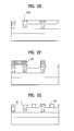
- FIGS. 2A to 2 Gare sectional views showing fabricating process steps of a semiconductor device based on a recessed SOI structure according to the present invention.
- FIGS. 2A to 2 Gare sectional views showing fabrication process steps of a semiconductor device based on a recessed SOI structure according to the present invention.
- a SOI substrate 200in which a field region, a cell region and a peripheral region are defined, is provided and has a three-layered structure of bulk silicon layer 21 , an SiO 2 layer 22 , and a single crystallization silicon layer 23 .
- a trenchis formed in the field region of the single crystallization silicon layer 23 , and device isolation films 27 a are formed within the trench.
- the peripheral regionis recessed, and a DRAM device 29 is formed on the cell region and the recessed peripheral region.
- the single crystallization silicon layer 23has a thickness of 700 ⁇ 1500 ⁇ for a partially depleted (PD) SOI device, and 700 ⁇ for a fully depleted (FD) SOI device.
- a first insulating film 24 and a second insulating film 25are sequentially deposited on the SOI substrate 200 , where the cell region and the peripheral region are defined.
- the first insulating film 24 and the second insulating film 25are then selectively removed to partially expose the single crystallization silicon layer 23 .
- the first insulating film 24is formed of an oxide film and the second insulating film 25 is formed of a nitride film.
- the SOI substrate 200is a wafer having a three-layered structure in which an SiO 2 layer 22 is interposed between single crystallization silicon layers 21 and 23 .
- the lower bulk silicon layer 21acts as a mechanical support, and the SiO 2 layer 22 , which is an electrical insulating layer, and the single crystallization silicon layer 23 of ultra-thin film are formed thereon.
- a subminiature integrated circuitwill be laid on the single crystallization silicon layer 23 .
- ZMRzone-melting recrystallization
- SIMOXseparation by implantation of oxygen
- Bwafer direct bonding
- SIMOXan SiO 2 layer is formed within a silicon material at a constant depth by implanting oxygen into a silicon wafer, and then performing annealing at a high temperature.
- WDB methoda junction surface between a wafer on which an oxide film is deposited and a bare wafer is formed to be thin, and the bare wafer is bonded to the wafer on which tile oxide film is deposited, by annealing process of high temperature.
- a field oxide film 26is formed on the peripheral region, i.e., on the exposed single crystallization silicon layer 23 , by an annealing oxidation process using the patterned first and second insulating films 24 and 25 as masks. Subsequently, as shown in FIG. 2C, the first and second insulating films 24 and 25 are selectively removed, and then a first insulating film pattern 24 a and a second insulating film pattern 25 a are formed in the cell region.
- the upper single crystallization silicon layer 23 of the SOI substrate 200is partially removed using the first and second insulating film patterns 24 a and 25 a and the field oxide film 26 as masks to form a trench 27 .
- a third insulating filmis formed on the entire surface, including the trench 27 , and then planarized to form the device isolation films 27 a .
- the photoresistis patterned by photolithography to remain on the cell region and the device isolation films. Tile remaining field oxide film 26 is removed using the patterned photoresist 28 as a mask.
- the SOI substrate having a recessed structureis formed in the peripheral region.
- the photoresist 28is removed, and a process for forming the DRAM device 29 is performed on the SOI substrate of the cell region and the recessed peripheral region, so that the cell region has bulk characteristics while the recessed single crystallization silicon layer 23 of the peripheral region has a controlled thickness.
- a PD SOI device or an FD SOI devicecan be obtained.
- the single crystallization silicon layer 23is partially recessed, and the FD SOI device and the PD SOI device can be formed according to a thickness of the single crystallization silicon layer 23 that remains in regions where it is not recessed. Where the remaining single crystallization silicon layer 23 has a thickness of 700 ⁇ 1500 ⁇ , the PD SOI device is formed. Where the remaining single crystallization silicon layer 23 has a thickness of 700 ⁇ , the FD SOI device is formed.
- the peripheral regionis recessed.
- the threshold voltagecan be controlled according to bulk Si characteristic in the cell region.
- the silicon epitaxial layeris partially recessed in the peripheral region.
- the FD SOI device and the PD SOI devicecan be formed according to the thickness of the remaining silicon epitaxial layer without being recessed. This reduces junction cap, thereby enabling high speed operation. Also, low operating voltage can be used.
- the cell regionis connected with the body in the peripheral region, and body contact is possible, thereby removing the “floating body” effect.
- the semiconductor device having the recessed SOI structurehas the following advantages.
- the peripheral regionis recessed in the DRAM based on the SOI structure, the cell region has bulk characteristics and the peripheral region has unique characteristics of the SOI structure. This dramatically reduces parasitic capacitance, thereby resulting in high operationed speed and low power consumption.
- the cell regionis connected to the peripheral region, body contact is possible, thereby eliminating the floating body effect.
- a substrate voltagecan be applied to the peripheral region without changing the layout, thereby improving operation stability of the device.
Landscapes
- Engineering & Computer Science (AREA)
- Manufacturing & Machinery (AREA)
- Physics & Mathematics (AREA)
- Condensed Matter Physics & Semiconductors (AREA)
- General Physics & Mathematics (AREA)
- Computer Hardware Design (AREA)
- Microelectronics & Electronic Packaging (AREA)
- Power Engineering (AREA)
- Semiconductor Memories (AREA)
- Element Separation (AREA)
- Thin Film Transistor (AREA)
Abstract
Description
1. Field of the Invention
The present invention relates to a semiconductor device, and more particularly, to a dynamic random access memory (DRAM) device based on a silicon on insulator (SOI) structure, and to a method for fabricating the same.
2. Background of the Related Art
Recently, processes for fabricating an integrated circuit device known as an SOI device have been developed. The SOI device is a semiconductor device fabricated within a thin silicon layer that covers an electrical insulating region formed on a substrate. The insulating region includes an SiO2layer deposited on a semiconductor substrate, such as silicon or gallium arsenide. A circuit that is electrically insulated from a lower substrate can then be formed using the SOI device.
The SOI device provides various advantages as compared with a conventional semiconductor device. For example, the SOI device generally consumes less power. Also, the SOI device has smaller parasitic capacitance, and thus operates at higher speeds. Furthermore, since the SOI device is less susceptible to adverse effects of ionization emission, it is more reliable in applications where ionization emission may cause operational error.
Recently, a structure where devices are arranged on both sides of a SOI substrate to reduce an area of a unit cell has been disclosed. The SOI technology is used to mutually isolate active devices by forming the active devices within individual silicon islands supported on an upper portion of an insulating substrate. Accordingly, the SOI structure has excellent high packing density and reduces the number of process steps as compared with a bulk silicon structure. As described above, the active device formed on the upper portion of the SOI substrate is called an SOI device. Since the SOI device has a dramatically reduced parasitic capacitance as compared with a bulk silicon device, high operational speed of a circuit and low power consumption can be obtained.
Unwanted charges are accumulated in a bulk (region) while a unit cell is floating and operating, so that the concentration of impurities in the bulk is reduced. In this case, a so-called “floating body” phenomenon, which varies a threshold value of a transistor, occurs. For this reason, a problem arises in that the unit cells do not operate uniformly.
A DRAM includes a memory cell array having a plurality of memory cells regularly arranged in X and Y directions, and a peripheral circuit formed around the memory cell array, for controlling the cells.
With an increase of packing density of a DRAM device, reduction of a unit cell area is required. It is becoming difficult to reduce a design rule of a unit cell due to limitation of photolithography process and degradation of electrical characteristic of a device. In this respect, many attempts to reduce an area of the unit cell in the same design rule by varying layout and sensing method of the cell have been made recently. Recently, to reduce the area of the unit cell, the SOI substrate has been used so that the devices are arranged at both sides of the SOI substrate.
A related art semiconductor device based on a SOI structure and method for fabricating the same will now be described with reference to the accompanying drawings.
As shown in FIGS. 1A and 1B, a DRAM device is formed on aSOI substrate 100 in whichdevice isolation films 14 are formed. The SOI substrate, as shown in FIG. 1B, has a three-layered structure in which an SiO2layer12 is interposed between Si single crystallization structures. Alower silicon layer 11 acts as a mechanical support, and the SiO2layer12, which is an electrical insulating layer, and an ultra-thin singlecrystallization silicon layer 13 are formed thereon. A subminiature integrated circuit will be laid on the singlecrystallization silicon layer 13.
In case where a transistor is formed in a cell region and a peripheral region based on the SOI substrate, the applied voltage is small due to reduction of well and load resistance. For this reason, the transistor can operate at low power. Also, the transistor has high operational speed. However, when a bias is applied to the substrate to control a threshold voltage of the transistor of the cell region, a threshold voltage of the peripheral region also needs to be high. For this reason, it is difficult for the peripheral region circuits to realize low power consumption and high reproducibility. As high packing density is required in the DRAM device, a device can be formed within a semiconductor substrate formed over a handle wafer with an insulating material interposed between the sermiconductor substrate and the handle wafer. Thus, limitation on packing density in the process can be overcome. For this reason, much attention has been centered on fabrication of a DRAM device having an SOI structure. Further, as described above, in SOI transistors, the applied voltage is small due to reduction of well and load resistance. For this reason, the transistor can operate at low power and at high speed.
However,the DRAM device having a SOI structure has several problems. One of the problems is the “floating body” effect. Since the active region of the transistor is electrically floating, the characteristics of the transistor are unstable, thereby causing malfunctions of the transistor and degradation of characteristics of the transistor.
Furthermore, in the SOI DRAM, to control the threshold voltage of the cell region, it is necessary to apply a substrate voltage. However, in the related semiconductor device based on an SOI structure, a substrate voltage is applied to the peripheral region as well as the cell region, thereby degrading the low pow-r characteristic and high reproducibility of the SOI device.
Accordingly, the present invention is directed to a semiconductor device having recessed SOI structure and a method for fabricating same that substantially obviates one or more of the problems due to limitations and disadvantages of the related art.
The inventions solves at least the above problems and/or disadvantages and provides at least the advantages described hereinafter.
An aspect of the present invention is to provide a semiconductor device having a recessed SOI structure and method for fabricating the same in which a substrate voltage is applied to a cell region to easily control a threshold voltage, and where a peripheral region is recessed to realize low power and high reproducibility.
Additional features and advantages of the invention will be set forth in the description which follows, and in part will be apparent from the description, or may be learned by practice of the invention. The advantages of the invention will be realized and attained by the structure particularly pointed out in the written description or its equivalents and claims hereof as well as the appended drawings.
To achieve at least these advantages in a whole or in part and in accordance with purposes of the present invention, as embodied and broadly described, a semiconductor device having a recessed silicon on insulator (SOI) structure includes an SOI substrate having a cell region, a peripheral region and a field region, the SOI substrate having a first semiconductor layer, an insulating layer on the first semiconductor layer, and a second semiconductor layer on the insulating layer, a trench in the field region of the second semiconductor layer, a device isolation film within the trench, a peripheral region recessed in the second semiconductor layer, and an active semiconductor device on the cell region and the peripheral region of the second semiconductor layer.
In another aspect, a method for fabricating a semiconductor device based on a SOI structure having an SOI substrate including a first semiconductor layer, an insulating layer on the first semiconductor layer, and a second semiconductor layer on the insulating layer, the semiconductor device having a cell region, a peripheral region and a field region, the method includes the steps of forming a field insulating film within the second semiconductor layer of the peripheral region and on a surface of the second semiconductor layer, forming a trench in the field region of the second semiconductor layer, forming a device isolation film within the trench, and removing the field insulating film to form a recessed peripheral region.
It is to be understood that both the foregoing general description and the following detailed description are exemplary and explanatory and are intended to provide further explanation of the invention as claimed.
The accompanying drawings, which are included to provide a further understanding of the invention and are incorporated in and constitute a part of this specification, illustrate embodiments of the invention and together with the description serve to explain the principles of the invention.
In the drawings:
FIG. 1A is a sectional view showing an SOI substrate;
FIG. 1B is a sectional view showing a structure of a related art semiconductor device based on the SOI substrate; and
FIGS. 2A to2G are sectional views showing fabricating process steps of a semiconductor device based on a recessed SOI structure according to the present invention.
Reference will now be made in detail to the preferred embodiments of the present invention, examples of which are illustrated in the accompanying drawings.
FIGS. 2A to2G are sectional views showing fabrication process steps of a semiconductor device based on a recessed SOI structure according to the present invention.
First, a structure of a semiconductor device based on a SOI structure will be described with reference to FIG.2G. As shown in FIG. 2G, aSOI substrate 200, in which a field region, a cell region and a peripheral region are defined, is provided and has a three-layered structure ofbulk silicon layer 21, an SiO2layer22, and a singlecrystallization silicon layer 23. A trench is formed in the field region of the singlecrystallization silicon layer 23, anddevice isolation films 27aare formed within the trench. The peripheral region is recessed, and aDRAM device 29 is formed on the cell region and the recessed peripheral region.
At this time, the singlecrystallization silicon layer 23 has a thickness of 700˜1500Å for a partially depleted (PD) SOI device, and 700Å for a fully depleted (FD) SOI device.
A method for fabricating the aforementioned semiconductor device having an SOI structure will now be described.
As shown in FIG. 2A, a first insulatingfilm 24 and a second insulatingfilm 25 are sequentially deposited on theSOI substrate 200, where the cell region and the peripheral region are defined. The first insulatingfilm 24 and the second insulatingfilm 25 are then selectively removed to partially expose the singlecrystallization silicon layer 23.
The first insulatingfilm 24 is formed of an oxide film and the second insulatingfilm 25 is formed of a nitride film.
TheSOI substrate 200 is a wafer having a three-layered structure in which an SiO2layer22 is interposed between single crystallization silicon layers21 and23. The lowerbulk silicon layer 21 acts as a mechanical support, and the SiO2layer22, which is an electrical insulating layer, and the singlecrystallization silicon layer 23 of ultra-thin film are formed thereon. A subminiature integrated circuit will be laid on the singlecrystallization silicon layer 23.
Three methods are commonly used for forming the SOI structure. There is a zone-melting recrystallization (ZMR) method, a separation by implantation of oxygen (SIMOX) method, and wafer direct bonding (B) method. In the SIMOX method, an SiO2layer is formed within a silicon material at a constant depth by implanting oxygen into a silicon wafer, and then performing annealing at a high temperature. In the WDB method, a junction surface between a wafer on which an oxide film is deposited and a bare wafer is formed to be thin, and the bare wafer is bonded to the wafer on which tile oxide film is deposited, by annealing process of high temperature.
As shown in FIG. 2B, afield oxide film 26 is formed on the peripheral region, i.e., on the exposed singlecrystallization silicon layer 23, by an annealing oxidation process using the patterned first and second insulatingfilms films insulating film pattern 24aand a secondinsulating film pattern 25aare formed in the cell region.
As shown in FIG. 2D, the upper singlecrystallization silicon layer 23 of theSOI substrate 200 is partially removed using the first and secondinsulating film patterns field oxide film 26 as masks to form atrench 27.
Subsequently, as shown in FIG. 2E, a third insulating film is formed on the entire surface, including thetrench 27, and then planarized to form thedevice isolation films 27a. As shown in FIG. 2F, the photoresist is patterned by photolithography to remain on the cell region and the device isolation films. Tile remainingfield oxide film 26 is removed using the patternedphotoresist 28 as a mask. Thus, the SOI substrate having a recessed structure is formed in the peripheral region.
As shown in FIG. 2G, thephotoresist 28 is removed, and a process for forming theDRAM device 29 is performed on the SOI substrate of the cell region and the recessed peripheral region, so that the cell region has bulk characteristics while the recessed singlecrystallization silicon layer 23 of the peripheral region has a controlled thickness. Thus, a PD SOI device or an FD SOI device can be obtained.
At this time, the singlecrystallization silicon layer 23 is partially recessed, and the FD SOI device and the PD SOI device can be formed according to a thickness of the singlecrystallization silicon layer 23 that remains in regions where it is not recessed. Where the remaining singlecrystallization silicon layer 23 has a thickness of 700˜1500 Å, the PD SOI device is formed. Where the remaining singlecrystallization silicon layer 23 has a thickness of 700 Å, the FD SOI device is formed.
Accordingly, to realize both the unique characteristics of the SOI device in the peripheral region and bulk characteristics in the cell region, the peripheral region is recessed.
Thus, the threshold voltage can be controlled according to bulk Si characteristic in the cell region. The silicon epitaxial layer is partially recessed in the peripheral region. The FD SOI device and the PD SOI device can be formed according to the thickness of the remaining silicon epitaxial layer without being recessed. This reduces junction cap, thereby enabling high speed operation. Also, low operating voltage can be used.
Furthermore, the cell region is connected with the body in the peripheral region, and body contact is possible, thereby removing the “floating body” effect.
The semiconductor device having the recessed SOI structure has the following advantages.
First, since the peripheral region is recessed in the DRAM based on the SOI structure, the cell region has bulk characteristics and the peripheral region has unique characteristics of the SOI structure. This dramatically reduces parasitic capacitance, thereby resulting in high operationed speed and low power consumption.
Furthermore, since the cell region is connected to the peripheral region, body contact is possible, thereby eliminating the floating body effect. As a result, a substrate voltage can be applied to the peripheral region without changing the layout, thereby improving operation stability of the device.
It will be apparent to those skilled in the art that various modifications and variations can be made in the present invention without departing from the spirit or scope of the invention. Thus, it is intended that the present invention cover the modifications and variations of this invention provided they come within the scope of the appended claims and their equivalents.
Claims (6)
1. A method for fabricating a semiconductor device based on a SOI structure having an SOI substrate including a first semiconductor layer, an insulating layer on the first semiconductor layer, and a second semiconductor layer on the insulating layer, the semiconductor device having a cell region, a peripheral region and a field region, the method comprising the steps of:
forming a field insulating film within the second semiconductor layer of the peripheral region and on a surface of the second semiconductor layer;
forming a trench in the field region of the second semiconductor layer;
forming a device isolation film within the trench; and
removing the field insulating film to form a recessed peripheral region.
2. The method ofclaim 1 , wherein the step of forming the field insulating film includes the steps of:
sequentially forming a first insulating film and a second insulating film on the SOI substrate, excluding the peripheral region; and
oxidizing the second semiconductor layer of the peripheral region using the first and second insulating films as masks.
3. The method ofclaim 1 , wherein the step of forming the trench includes the steps of:
patterning and removing the first and second insulating films on the field region; and
selectively removing the second semiconductor layer using the patterned first and second insulating films and the field insulating film as masks.
4. The method ofclaim 1 , wherein the step of forming the device isolation films includes the steps of:
forming an insulating film on the entire surface including the trench; and
planarizing the insulating film by chemical mechanical polishing (CMP).
5. The method ofclaim 1 , wherein the second semiconductor layer that remains without being recessed in the peripheral region has a thickness of approximately 700 to 1500 Å.
6. The method ofclaim 1 , wherein the second semiconductor layer that remains without being recessed in the peripheral region has a thickness of approximately 700 Å.
Applications Claiming Priority (2)
| Application Number | Priority Date | Filing Date | Title |
|---|---|---|---|
| KRP00-41986 | 2000-07-21 | ||
| KR1020000041986AKR100339425B1 (en) | 2000-07-21 | 2000-07-21 | Semiconductor device and Method for Manufacturing with recessed SOI structure |
Publications (1)
| Publication Number | Publication Date |
|---|---|
| US6403435B1true US6403435B1 (en) | 2002-06-11 |
Family
ID=19679241
Family Applications (1)
| Application Number | Title | Priority Date | Filing Date |
|---|---|---|---|
| US09/722,518Expired - Fee RelatedUS6403435B1 (en) | 2000-07-21 | 2000-11-28 | Method for fabricating a semiconductor device having recessed SOI structure |
Country Status (2)
| Country | Link |
|---|---|
| US (1) | US6403435B1 (en) |
| KR (1) | KR100339425B1 (en) |
Cited By (67)
| Publication number | Priority date | Publication date | Assignee | Title |
|---|---|---|---|---|
| US20030057489A1 (en)* | 2001-08-23 | 2003-03-27 | Seiko Epson Corporation | Method for manufacturing semiconductor substrate, semiconductor substrate, electrooptic device and electronic apparatus |
| US20040124488A1 (en)* | 2001-06-18 | 2004-07-01 | Pierre Fazan | Semiconductor device |
| US20040180478A1 (en)* | 2003-03-12 | 2004-09-16 | Taiwan Semiconductor Manufacturing Company | Silicon-on-insulator ulsi devices with multiple silicon film thicknesses |
| US20040228168A1 (en)* | 2003-05-13 | 2004-11-18 | Richard Ferrant | Semiconductor memory device and method of operating same |
| US20040227166A1 (en)* | 2003-05-13 | 2004-11-18 | Lionel Portmann | Reference current generator, and method of programming, adjusting and/or operating same |
| US20040238890A1 (en)* | 2002-04-18 | 2004-12-02 | Pierre Fazan | Semiconductor device |
| US20040240306A1 (en)* | 2002-04-18 | 2004-12-02 | Pierre Fazan | Data storage device and refreshing method for use with such device |
| US20040262693A1 (en)* | 2003-06-30 | 2004-12-30 | Kabushiki Kaisha Toshiba | Semiconductor storage device and semiconductor integrated circuit |
| US20050013163A1 (en)* | 2003-05-13 | 2005-01-20 | Richard Ferrant | Semiconductor memory cell, array, architecture and device, and method of operating same |
| US20050017240A1 (en)* | 2003-07-22 | 2005-01-27 | Pierre Fazan | Integrated circuit device, and method of fabricating same |
| US20050063224A1 (en)* | 2003-09-24 | 2005-03-24 | Pierre Fazan | Low power programming technique for a floating body memory transistor, memory cell, and memory array |
| US20060091462A1 (en)* | 2004-11-04 | 2006-05-04 | Serguei Okhonin | Memory cell having an electrically floating body transistor and programming technique therefor |
| US20060098481A1 (en)* | 2004-11-10 | 2006-05-11 | Serguei Okhonin | Circuitry for and method of improving statistical distribution of integrated circuits |
| US20060126374A1 (en)* | 2004-12-13 | 2006-06-15 | Waller William K | Sense amplifier circuitry and architecture to write data into and/or read from memory cells |
| US20060128074A1 (en)* | 2004-12-13 | 2006-06-15 | Texas Instruments Incorporated | Combined fully-depleted silicon-on-insulator (FD-SOI) and partially-depleted silicon-on-insulator (PD-SOI)devices |
| US20060131650A1 (en)* | 2004-12-22 | 2006-06-22 | Serguei Okhonin | Bipolar reading technique for a memory cell having an electrically floating body transistor |
| US20070023833A1 (en)* | 2005-07-28 | 2007-02-01 | Serguei Okhonin | Method for reading a memory cell having an electrically floating body transistor, and memory cell and array implementing same |
| US20070058427A1 (en)* | 2005-09-07 | 2007-03-15 | Serguei Okhonin | Memory cell and memory cell array having an electrically floating body transistor, and methods of operating same |
| US20070064489A1 (en)* | 2005-09-19 | 2007-03-22 | Philippe Bauser | Method and circuitry to generate a reference current for reading a memory cell, and device implementing same |
| US20070085140A1 (en)* | 2005-10-19 | 2007-04-19 | Cedric Bassin | One transistor memory cell having strained electrically floating body region, and method of operating same |
| US20070138530A1 (en)* | 2005-12-19 | 2007-06-21 | Serguei Okhonin | Electrically floating body memory cell and array, and method of operating or controlling same |
| US20070187775A1 (en)* | 2006-02-16 | 2007-08-16 | Serguei Okhonin | Multi-bit memory cell having electrically floating body transistor, and method of programming and reading same |
| US20070235806A1 (en)* | 2006-04-07 | 2007-10-11 | Joshi Rajiv V | Integrated circuit chip with fets having mixed body thicknesses and method of manufacture thereof |
| US20070285982A1 (en)* | 2006-04-07 | 2007-12-13 | Eric Carman | Memory array having a programmable word length, and method of operating same |
| US20080013359A1 (en)* | 2006-07-11 | 2008-01-17 | David Fisch | Integrated circuit including memory array having a segmented bit line architecture and method of controlling and/or operating same |
| US20090201723A1 (en)* | 2008-02-06 | 2009-08-13 | Serguei Okhonin | Single Transistor Memory Cell |
| US7606098B2 (en) | 2006-04-18 | 2009-10-20 | Innovative Silicon Isi Sa | Semiconductor memory array architecture with grouped memory cells, and method of controlling same |
| US20100142294A1 (en)* | 2008-12-05 | 2010-06-10 | Eric Carman | Vertical Transistor Memory Cell and Array |
| US20100296327A1 (en)* | 2009-05-22 | 2010-11-25 | Innovative Silicon Isi Sa | Techniques for providing a direct injection semiconductor memory device |
| US7924630B2 (en) | 2008-10-15 | 2011-04-12 | Micron Technology, Inc. | Techniques for simultaneously driving a plurality of source lines |
| US7933140B2 (en) | 2008-10-02 | 2011-04-26 | Micron Technology, Inc. | Techniques for reducing a voltage swing |
| US7933142B2 (en) | 2006-05-02 | 2011-04-26 | Micron Technology, Inc. | Semiconductor memory cell and array using punch-through to program and read same |
| US7947543B2 (en) | 2008-09-25 | 2011-05-24 | Micron Technology, Inc. | Recessed gate silicon-on-insulator floating body device with self-aligned lateral isolation |
| US20110122687A1 (en)* | 2009-11-24 | 2011-05-26 | Innovative Silicon Isi Sa | Techniques for reducing disturbance in a semiconductor device |
| US7957206B2 (en) | 2008-04-04 | 2011-06-07 | Micron Technology, Inc. | Read circuitry for an integrated circuit having memory cells and/or a memory cell array, and method of operating same |
| US20110133283A1 (en)* | 2009-12-09 | 2011-06-09 | Hynix Semiconductor Inc. | Semiconductor device and method for forming the same |
| US8064274B2 (en) | 2007-05-30 | 2011-11-22 | Micron Technology, Inc. | Integrated circuit having voltage generation circuitry for memory cell array, and method of operating and/or controlling same |
| US8069377B2 (en) | 2006-06-26 | 2011-11-29 | Micron Technology, Inc. | Integrated circuit having memory array including ECC and column redundancy and method of operating the same |
| US8085594B2 (en) | 2007-06-01 | 2011-12-27 | Micron Technology, Inc. | Reading technique for memory cell with electrically floating body transistor |
| US8139418B2 (en) | 2009-04-27 | 2012-03-20 | Micron Technology, Inc. | Techniques for controlling a direct injection semiconductor memory device |
| US8189376B2 (en) | 2008-02-08 | 2012-05-29 | Micron Technology, Inc. | Integrated circuit having memory cells including gate material having high work function, and method of manufacturing same |
| US8194487B2 (en) | 2007-09-17 | 2012-06-05 | Micron Technology, Inc. | Refreshing data of memory cells with electrically floating body transistors |
| US8199595B2 (en) | 2009-09-04 | 2012-06-12 | Micron Technology, Inc. | Techniques for sensing a semiconductor memory device |
| US8223574B2 (en) | 2008-11-05 | 2012-07-17 | Micron Technology, Inc. | Techniques for block refreshing a semiconductor memory device |
| US8264041B2 (en) | 2007-01-26 | 2012-09-11 | Micron Technology, Inc. | Semiconductor device with electrically floating body |
| US8310893B2 (en) | 2009-12-16 | 2012-11-13 | Micron Technology, Inc. | Techniques for reducing impact of array disturbs in a semiconductor memory device |
| US8315099B2 (en) | 2009-07-27 | 2012-11-20 | Micron Technology, Inc. | Techniques for providing a direct injection semiconductor memory device |
| US8319294B2 (en) | 2009-02-18 | 2012-11-27 | Micron Technology, Inc. | Techniques for providing a source line plane |
| US8349662B2 (en) | 2007-12-11 | 2013-01-08 | Micron Technology, Inc. | Integrated circuit having memory cell array, and method of manufacturing same |
| US8369177B2 (en) | 2010-03-05 | 2013-02-05 | Micron Technology, Inc. | Techniques for reading from and/or writing to a semiconductor memory device |
| US8411513B2 (en) | 2010-03-04 | 2013-04-02 | Micron Technology, Inc. | Techniques for providing a semiconductor memory device having hierarchical bit lines |
| US8411524B2 (en) | 2010-05-06 | 2013-04-02 | Micron Technology, Inc. | Techniques for refreshing a semiconductor memory device |
| US8416636B2 (en) | 2010-02-12 | 2013-04-09 | Micron Technology, Inc. | Techniques for controlling a semiconductor memory device |
| US20130089957A1 (en)* | 2011-03-21 | 2013-04-11 | United Microelectronics Corporation | Fin field-effect transistor structure and manufacturing process thereof |
| US20130087849A1 (en)* | 2008-12-30 | 2013-04-11 | Micron Technology, Inc. | Method of fabricating a charge trap nand flash memory device |
| US8508994B2 (en) | 2009-04-30 | 2013-08-13 | Micron Technology, Inc. | Semiconductor device with floating gate and electrically floating body |
| US8518774B2 (en) | 2007-03-29 | 2013-08-27 | Micron Technology, Inc. | Manufacturing process for zero-capacitor random access memory circuits |
| US8531878B2 (en) | 2011-05-17 | 2013-09-10 | Micron Technology, Inc. | Techniques for providing a semiconductor memory device |
| US8536628B2 (en) | 2007-11-29 | 2013-09-17 | Micron Technology, Inc. | Integrated circuit having memory cell array including barriers, and method of manufacturing same |
| US8537610B2 (en) | 2009-07-10 | 2013-09-17 | Micron Technology, Inc. | Techniques for providing a semiconductor memory device |
| US8547738B2 (en) | 2010-03-15 | 2013-10-01 | Micron Technology, Inc. | Techniques for providing a semiconductor memory device |
| US8576631B2 (en) | 2010-03-04 | 2013-11-05 | Micron Technology, Inc. | Techniques for sensing a semiconductor memory device |
| US8710566B2 (en) | 2009-03-04 | 2014-04-29 | Micron Technology, Inc. | Techniques for forming a contact to a buried diffusion layer in a semiconductor memory device |
| US8748959B2 (en) | 2009-03-31 | 2014-06-10 | Micron Technology, Inc. | Semiconductor memory device |
| US8773933B2 (en) | 2012-03-16 | 2014-07-08 | Micron Technology, Inc. | Techniques for accessing memory cells |
| US9559216B2 (en) | 2011-06-06 | 2017-01-31 | Micron Technology, Inc. | Semiconductor memory device and method for biasing same |
| US11011547B2 (en)* | 2018-04-24 | 2021-05-18 | X-Fab France | Method for forming a microelectronic device |
Citations (6)
| Publication number | Priority date | Publication date | Assignee | Title |
|---|---|---|---|---|
| JP2000091534A (en)* | 1998-09-11 | 2000-03-31 | Mitsubishi Electric Corp | Semiconductor device |
| US6091112A (en) | 1996-12-24 | 2000-07-18 | Lg Semicon Co., Ltd. | Silicon on insulator semiconductor substrate and fabrication method therefor |
| US6190952B1 (en)* | 1999-03-03 | 2001-02-20 | Advanced Micro Devices, Inc. | Multiple semiconductor-on-insulator threshold voltage circuit |
| US6235567B1 (en)* | 1999-08-31 | 2001-05-22 | International Business Machines Corporation | Silicon-germanium bicmos on soi |
| US6238967B1 (en)* | 1999-04-12 | 2001-05-29 | Motorola, Inc. | Method of forming embedded DRAM structure |
| US6300172B1 (en)* | 1999-10-01 | 2001-10-09 | Chartered Semiconductor Manufacturing Ltd. | Method of field isolation in silicon-on-insulator technology |
Family Cites Families (6)
| Publication number | Priority date | Publication date | Assignee | Title |
|---|---|---|---|---|
| JPH0727974B2 (en)* | 1988-04-26 | 1995-03-29 | 三菱電機株式会社 | Method of manufacturing semiconductor memory device |
| JP3279000B2 (en)* | 1993-09-27 | 2002-04-30 | ソニー株式会社 | Semiconductor device manufacturing method |
| JP2806286B2 (en)* | 1995-02-07 | 1998-09-30 | 日本電気株式会社 | Semiconductor device |
| KR0179794B1 (en)* | 1995-12-28 | 1999-03-20 | 문정환 | Well-forming method of semiconductor device |
| JPH11284137A (en)* | 1998-03-30 | 1999-10-15 | Nippon Steel Corp | Semiconductor memory device and method of manufacturing the same |
| JPH11317506A (en)* | 1998-05-01 | 1999-11-16 | Nippon Steel Corp | Semiconductor device and manufacturing method thereof |
- 2000
- 2000-07-21KRKR1020000041986Apatent/KR100339425B1/ennot_activeExpired - Fee Related
- 2000-11-28USUS09/722,518patent/US6403435B1/ennot_activeExpired - Fee Related
Patent Citations (6)
| Publication number | Priority date | Publication date | Assignee | Title |
|---|---|---|---|---|
| US6091112A (en) | 1996-12-24 | 2000-07-18 | Lg Semicon Co., Ltd. | Silicon on insulator semiconductor substrate and fabrication method therefor |
| JP2000091534A (en)* | 1998-09-11 | 2000-03-31 | Mitsubishi Electric Corp | Semiconductor device |
| US6190952B1 (en)* | 1999-03-03 | 2001-02-20 | Advanced Micro Devices, Inc. | Multiple semiconductor-on-insulator threshold voltage circuit |
| US6238967B1 (en)* | 1999-04-12 | 2001-05-29 | Motorola, Inc. | Method of forming embedded DRAM structure |
| US6235567B1 (en)* | 1999-08-31 | 2001-05-22 | International Business Machines Corporation | Silicon-germanium bicmos on soi |
| US6300172B1 (en)* | 1999-10-01 | 2001-10-09 | Chartered Semiconductor Manufacturing Ltd. | Method of field isolation in silicon-on-insulator technology |
Cited By (196)
| Publication number | Priority date | Publication date | Assignee | Title |
|---|---|---|---|---|
| US6969662B2 (en) | 2001-06-18 | 2005-11-29 | Pierre Fazan | Semiconductor device |
| US20050213379A1 (en)* | 2001-06-18 | 2005-09-29 | Pierre Fazan | Semiconductor device |
| US20040135202A1 (en)* | 2001-06-18 | 2004-07-15 | Pierre Fazan | Semiconductor device |
| US20040159876A1 (en)* | 2001-06-18 | 2004-08-19 | Pierre Fazan | Semiconductor device |
| US7280399B2 (en) | 2001-06-18 | 2007-10-09 | Innovative Silicon S.A. | Semiconductor device |
| US7239549B2 (en) | 2001-06-18 | 2007-07-03 | Innovative Silicon S.A. | Semiconductor device |
| US20050280028A1 (en)* | 2001-06-18 | 2005-12-22 | Pierre Fazan | Semiconductor device |
| US7732816B2 (en) | 2001-06-18 | 2010-06-08 | Innovative Silicon Isi Sa | Semiconductor device |
| US20040124488A1 (en)* | 2001-06-18 | 2004-07-01 | Pierre Fazan | Semiconductor device |
| US6925006B2 (en) | 2001-06-18 | 2005-08-02 | Innovative Silicon S.A. | Semiconductor device |
| US20080055974A1 (en)* | 2001-06-18 | 2008-03-06 | Pierre Fazan | Semiconductor device |
| US20080068882A1 (en)* | 2001-06-18 | 2008-03-20 | Pierre Fazan | Semiconductor device |
| US7541616B2 (en) | 2001-06-18 | 2009-06-02 | Innovative Silicon Isi Sa | Semiconductor device |
| US6873539B1 (en) | 2001-06-18 | 2005-03-29 | Pierre Fazan | Semiconductor device |
| US6937516B2 (en) | 2001-06-18 | 2005-08-30 | Innovative Silicon S.A. | Semiconductor device |
| US6934186B2 (en) | 2001-06-18 | 2005-08-23 | Innovative Silicon S.A. | Semiconductor device |
| US6930918B2 (en) | 2001-06-18 | 2005-08-16 | Innovative Silicon S.A. | Semiconductor device |
| US20030057489A1 (en)* | 2001-08-23 | 2003-03-27 | Seiko Epson Corporation | Method for manufacturing semiconductor substrate, semiconductor substrate, electrooptic device and electronic apparatus |
| US20040238890A1 (en)* | 2002-04-18 | 2004-12-02 | Pierre Fazan | Semiconductor device |
| US7514748B2 (en) | 2002-04-18 | 2009-04-07 | Innovative Silicon Isi Sa | Semiconductor device |
| US7170807B2 (en) | 2002-04-18 | 2007-01-30 | Innovative Silicon S.A. | Data storage device and refreshing method for use with such device |
| US20050128851A1 (en)* | 2002-04-18 | 2005-06-16 | Pierre Fazan | Data storage device and refreshing method for use with such device |
| US7342842B2 (en) | 2002-04-18 | 2008-03-11 | Innovative Silicon, S.A. | Data storage device and refreshing method for use with such device |
| US20040240306A1 (en)* | 2002-04-18 | 2004-12-02 | Pierre Fazan | Data storage device and refreshing method for use with such device |
| US7061050B2 (en) | 2002-04-18 | 2006-06-13 | Innovative Silicon S.A. | Semiconductor device utilizing both fully and partially depleted devices |
| US20070109896A1 (en)* | 2002-04-18 | 2007-05-17 | Pierre Fazan | Data storage device and refreshing method for use with such device |
| US6982918B2 (en) | 2002-04-18 | 2006-01-03 | Pierre Fazan | Data storage device and refreshing method for use with such device |
| US7141459B2 (en)* | 2003-03-12 | 2006-11-28 | Taiwan Semiconductor Manufacturing Company, Ltd. | Silicon-on-insulator ULSI devices with multiple silicon film thicknesses |
| US20040180478A1 (en)* | 2003-03-12 | 2004-09-16 | Taiwan Semiconductor Manufacturing Company | Silicon-on-insulator ulsi devices with multiple silicon film thicknesses |
| US6980461B2 (en) | 2003-05-13 | 2005-12-27 | Innovative Silicon S.A. | Reference current generator, and method of programming, adjusting and/or operating same |
| US20050013163A1 (en)* | 2003-05-13 | 2005-01-20 | Richard Ferrant | Semiconductor memory cell, array, architecture and device, and method of operating same |
| US20070159911A1 (en)* | 2003-05-13 | 2007-07-12 | Richard Ferrant | Semiconductor memory device and method of operating same |
| US7733693B2 (en) | 2003-05-13 | 2010-06-08 | Innovative Silicon Isi Sa | Semiconductor memory device and method of operating same |
| US20040228168A1 (en)* | 2003-05-13 | 2004-11-18 | Richard Ferrant | Semiconductor memory device and method of operating same |
| US20040227166A1 (en)* | 2003-05-13 | 2004-11-18 | Lionel Portmann | Reference current generator, and method of programming, adjusting and/or operating same |
| US20050174873A1 (en)* | 2003-05-13 | 2005-08-11 | Richard Ferrant | Semiconductor memory device and method of operating same |
| US20050162931A1 (en)* | 2003-05-13 | 2005-07-28 | Lionel Portmann | Reference current generator, and method of programming, adjusting and/or operating same |
| US7359229B2 (en) | 2003-05-13 | 2008-04-15 | Innovative Silicon S.A. | Semiconductor memory device and method of operating same |
| US7085156B2 (en) | 2003-05-13 | 2006-08-01 | Innovative Silicon S.A. | Semiconductor memory device and method of operating same |
| US7085153B2 (en) | 2003-05-13 | 2006-08-01 | Innovative Silicon S.A. | Semiconductor memory cell, array, architecture and device, and method of operating same |
| US20050157580A1 (en)* | 2003-05-13 | 2005-07-21 | Richard Ferrant | Semiconductor memory device and method of operating same |
| US6912150B2 (en) | 2003-05-13 | 2005-06-28 | Lionel Portman | Reference current generator, and method of programming, adjusting and/or operating same |
| US7187581B2 (en) | 2003-05-13 | 2007-03-06 | Innovative Silicon S.A. | Semiconductor memory device and method of operating same |
| US20080205114A1 (en)* | 2003-05-13 | 2008-08-28 | Richard Ferrant | Semiconductor memory device and method of operating same |
| US7425746B2 (en) | 2003-06-30 | 2008-09-16 | Kabushiki Kaisha Toshiba | Semiconductor storage device and semiconductor integrated circuit |
| US20060131660A1 (en)* | 2003-06-30 | 2006-06-22 | Kabushiki Kaisha Toshiba | Semiconductor storage device and semiconductor integrated circuit |
| US20040262693A1 (en)* | 2003-06-30 | 2004-12-30 | Kabushiki Kaisha Toshiba | Semiconductor storage device and semiconductor integrated circuit |
| US7638840B2 (en) | 2003-06-30 | 2009-12-29 | Kabushiki Kaisha Toshiba | Semiconductor storage device and semiconductor integrated circuit |
| EP1494288A3 (en)* | 2003-06-30 | 2005-12-14 | Kabushiki Kaisha Toshiba | Semiconductor storage device and semiconductor integrated circuit |
| US7023054B2 (en) | 2003-06-30 | 2006-04-04 | Kabushiki Kaisha Toshiba | Semiconductor storage device and semiconductor integrated circuit |
| US20080153213A1 (en)* | 2003-07-22 | 2008-06-26 | Pierre Fazan | Integrated circuit device, and method of fabricating same |
| US20050017240A1 (en)* | 2003-07-22 | 2005-01-27 | Pierre Fazan | Integrated circuit device, and method of fabricating same |
| US7736959B2 (en) | 2003-07-22 | 2010-06-15 | Innovative Silicon Isi Sa | Integrated circuit device, and method of fabricating same |
| US7335934B2 (en) | 2003-07-22 | 2008-02-26 | Innovative Silicon S.A. | Integrated circuit device, and method of fabricating same |
| US20060114717A1 (en)* | 2003-09-24 | 2006-06-01 | Pierre Fazan | Low power programming technique for a floating body memory transistor, memory cell, and memory array |
| US20050063224A1 (en)* | 2003-09-24 | 2005-03-24 | Pierre Fazan | Low power programming technique for a floating body memory transistor, memory cell, and memory array |
| US7177175B2 (en) | 2003-09-24 | 2007-02-13 | Innovative Silicon S.A. | Low power programming technique for a floating body memory transistor, memory cell, and memory array |
| US7184298B2 (en) | 2003-09-24 | 2007-02-27 | Innovative Silicon S.A. | Low power programming technique for a floating body memory transistor, memory cell, and memory array |
| US7476939B2 (en) | 2004-11-04 | 2009-01-13 | Innovative Silicon Isi Sa | Memory cell having an electrically floating body transistor and programming technique therefor |
| US20060091462A1 (en)* | 2004-11-04 | 2006-05-04 | Serguei Okhonin | Memory cell having an electrically floating body transistor and programming technique therefor |
| US7251164B2 (en) | 2004-11-10 | 2007-07-31 | Innovative Silicon S.A. | Circuitry for and method of improving statistical distribution of integrated circuits |
| US20060098481A1 (en)* | 2004-11-10 | 2006-05-11 | Serguei Okhonin | Circuitry for and method of improving statistical distribution of integrated circuits |
| US20060126374A1 (en)* | 2004-12-13 | 2006-06-15 | Waller William K | Sense amplifier circuitry and architecture to write data into and/or read from memory cells |
| US7486563B2 (en) | 2004-12-13 | 2009-02-03 | Innovative Silicon Isi Sa | Sense amplifier circuitry and architecture to write data into and/or read from memory cells |
| US7301838B2 (en) | 2004-12-13 | 2007-11-27 | Innovative Silicon S.A. | Sense amplifier circuitry and architecture to write data into and/or read from memory cells |
| US20060128074A1 (en)* | 2004-12-13 | 2006-06-15 | Texas Instruments Incorporated | Combined fully-depleted silicon-on-insulator (FD-SOI) and partially-depleted silicon-on-insulator (PD-SOI)devices |
| US7198993B2 (en)* | 2004-12-13 | 2007-04-03 | Texas Instruments Incorporated | Method of fabricating a combined fully-depleted silicon-on-insulator (FD-SOI) and partially-depleted silicon-on-insulator (PD-SOI) devices |
| US7301803B2 (en) | 2004-12-22 | 2007-11-27 | Innovative Silicon S.A. | Bipolar reading technique for a memory cell having an electrically floating body transistor |
| US20080025083A1 (en)* | 2004-12-22 | 2008-01-31 | Serguei Okhonin | Bipolar reading technique for a memory cell having an electrically floating body transistor |
| US20060131650A1 (en)* | 2004-12-22 | 2006-06-22 | Serguei Okhonin | Bipolar reading technique for a memory cell having an electrically floating body transistor |
| US7477540B2 (en) | 2004-12-22 | 2009-01-13 | Innovative Silicon Isi Sa | Bipolar reading technique for a memory cell having an electrically floating body transistor |
| US20070023833A1 (en)* | 2005-07-28 | 2007-02-01 | Serguei Okhonin | Method for reading a memory cell having an electrically floating body transistor, and memory cell and array implementing same |
| US20100020597A1 (en)* | 2005-09-07 | 2010-01-28 | Serguei Okhonin | Memory Cell and Memory Cell Array Having an Electrically Floating Body Transistor, and Methods of Operating Same |
| US7606066B2 (en) | 2005-09-07 | 2009-10-20 | Innovative Silicon Isi Sa | Memory cell and memory cell array having an electrically floating body transistor, and methods of operating same |
| US20070058427A1 (en)* | 2005-09-07 | 2007-03-15 | Serguei Okhonin | Memory cell and memory cell array having an electrically floating body transistor, and methods of operating same |
| US11031069B2 (en) | 2005-09-07 | 2021-06-08 | Ovonyx Memory Technology, Llc | Memory cell and memory cell array having an electrically floating body transistor, and methods of operating same |
| US10418091B2 (en) | 2005-09-07 | 2019-09-17 | Ovonyx Memory Technology, Llc | Memory cell and memory cell array having an electrically floating body transistor, and methods of operating same |
| US8873283B2 (en) | 2005-09-07 | 2014-10-28 | Micron Technology, Inc. | Memory cell and memory cell array having an electrically floating body transistor, and methods of operating same |
| US20070064489A1 (en)* | 2005-09-19 | 2007-03-22 | Philippe Bauser | Method and circuitry to generate a reference current for reading a memory cell, and device implementing same |
| US7499358B2 (en) | 2005-09-19 | 2009-03-03 | Innovative Silicon Isi Sa | Method and circuitry to generate a reference current for reading a memory cell, and device implementing same |
| US7355916B2 (en) | 2005-09-19 | 2008-04-08 | Innovative Silicon S.A. | Method and circuitry to generate a reference current for reading a memory cell, and device implementing same |
| US20070085140A1 (en)* | 2005-10-19 | 2007-04-19 | Cedric Bassin | One transistor memory cell having strained electrically floating body region, and method of operating same |
| US7683430B2 (en) | 2005-12-19 | 2010-03-23 | Innovative Silicon Isi Sa | Electrically floating body memory cell and array, and method of operating or controlling same |
| US20070138530A1 (en)* | 2005-12-19 | 2007-06-21 | Serguei Okhonin | Electrically floating body memory cell and array, and method of operating or controlling same |
| US20070187775A1 (en)* | 2006-02-16 | 2007-08-16 | Serguei Okhonin | Multi-bit memory cell having electrically floating body transistor, and method of programming and reading same |
| US7542345B2 (en) | 2006-02-16 | 2009-06-02 | Innovative Silicon Isi Sa | Multi-bit memory cell having electrically floating body transistor, and method of programming and reading same |
| US7940559B2 (en) | 2006-04-07 | 2011-05-10 | Micron Technology, Inc. | Memory array having a programmable word length, and method of operating same |
| US7285480B1 (en)* | 2006-04-07 | 2007-10-23 | International Business Machines Corporation | Integrated circuit chip with FETs having mixed body thicknesses and method of manufacture thereof |
| US20090302387A1 (en)* | 2006-04-07 | 2009-12-10 | International Business Machines Corporation | Integrated circuit chip with fets having mixed body thicknesses and method of manufacture thereof |
| US8134867B2 (en) | 2006-04-07 | 2012-03-13 | Micron Technology, Inc. | Memory array having a programmable word length, and method of operating same |
| US7492632B2 (en) | 2006-04-07 | 2009-02-17 | Innovative Silicon Isi Sa | Memory array having a programmable word length, and method of operating same |
| US7968944B2 (en)* | 2006-04-07 | 2011-06-28 | International Business Machines Corporation | Integrated circuit chip with FETs having mixed body thicknesses and method of manufacture thereof |
| US20070235806A1 (en)* | 2006-04-07 | 2007-10-11 | Joshi Rajiv V | Integrated circuit chip with fets having mixed body thicknesses and method of manufacture thereof |
| US20080026512A1 (en)* | 2006-04-07 | 2008-01-31 | International Business Machines Corporation | Integrated circuit chip with fets having mixed body thicknesses and method of manufacture thereof |
| US7521760B2 (en) | 2006-04-07 | 2009-04-21 | International Business Machines Corporation | Integrated circuit chip with FETs having mixed body thickness and method of manufacture thereof |
| US20070285982A1 (en)* | 2006-04-07 | 2007-12-13 | Eric Carman | Memory array having a programmable word length, and method of operating same |
| US20070257314A1 (en)* | 2006-04-07 | 2007-11-08 | International Business Machines Corporation | Integrated circuit chip with fets having mixed body thicknesses and method of manufacture thereof |
| US7606098B2 (en) | 2006-04-18 | 2009-10-20 | Innovative Silicon Isi Sa | Semiconductor memory array architecture with grouped memory cells, and method of controlling same |
| US8295078B2 (en) | 2006-05-02 | 2012-10-23 | Micron Technology, Inc. | Semiconductor memory cell and array using punch-through to program and read same |
| US7933142B2 (en) | 2006-05-02 | 2011-04-26 | Micron Technology, Inc. | Semiconductor memory cell and array using punch-through to program and read same |
| US8402326B2 (en) | 2006-06-26 | 2013-03-19 | Micron Technology, Inc. | Integrated circuit having memory array including ECC and column redundancy and method of operating same |
| US8069377B2 (en) | 2006-06-26 | 2011-11-29 | Micron Technology, Inc. | Integrated circuit having memory array including ECC and column redundancy and method of operating the same |
| US20080013359A1 (en)* | 2006-07-11 | 2008-01-17 | David Fisch | Integrated circuit including memory array having a segmented bit line architecture and method of controlling and/or operating same |
| US8395937B2 (en) | 2006-07-11 | 2013-03-12 | Micron Technology, Inc. | Integrated circuit including memory array having a segmented bit line architecture and method of controlling and/or operating same |
| US7542340B2 (en) | 2006-07-11 | 2009-06-02 | Innovative Silicon Isi Sa | Integrated circuit including memory array having a segmented bit line architecture and method of controlling and/or operating same |
| US7969779B2 (en) | 2006-07-11 | 2011-06-28 | Micron Technology, Inc. | Integrated circuit including memory array having a segmented bit line architecture and method of controlling and/or operating same |
| US8796770B2 (en) | 2007-01-26 | 2014-08-05 | Micron Technology, Inc. | Semiconductor device with electrically floating body |
| US8492209B2 (en) | 2007-01-26 | 2013-07-23 | Micron Technology, Inc. | Semiconductor device with electrically floating body |
| US8264041B2 (en) | 2007-01-26 | 2012-09-11 | Micron Technology, Inc. | Semiconductor device with electrically floating body |
| US9276000B2 (en) | 2007-03-29 | 2016-03-01 | Micron Technology, Inc. | Manufacturing process for zero-capacitor random access memory circuits |
| US8518774B2 (en) | 2007-03-29 | 2013-08-27 | Micron Technology, Inc. | Manufacturing process for zero-capacitor random access memory circuits |
| US8659956B2 (en) | 2007-05-30 | 2014-02-25 | Micron Technology, Inc. | Integrated circuit having voltage generation circuitry for memory cell array, and method of operating and/or controlling same |
| US8064274B2 (en) | 2007-05-30 | 2011-11-22 | Micron Technology, Inc. | Integrated circuit having voltage generation circuitry for memory cell array, and method of operating and/or controlling same |
| US9257155B2 (en) | 2007-05-30 | 2016-02-09 | Micron Technology, Inc. | Integrated circuit having voltage generation circuitry for memory cell array, and method of operating and/or controlling same |
| US8659948B2 (en) | 2007-06-01 | 2014-02-25 | Micron Technology, Inc. | Techniques for reading a memory cell with electrically floating body transistor |
| US8085594B2 (en) | 2007-06-01 | 2011-12-27 | Micron Technology, Inc. | Reading technique for memory cell with electrically floating body transistor |
| US8194487B2 (en) | 2007-09-17 | 2012-06-05 | Micron Technology, Inc. | Refreshing data of memory cells with electrically floating body transistors |
| US8797819B2 (en) | 2007-09-17 | 2014-08-05 | Micron Technology, Inc. | Refreshing data of memory cells with electrically floating body transistors |
| US8446794B2 (en) | 2007-09-17 | 2013-05-21 | Micron Technology, Inc. | Refreshing data of memory cells with electrically floating body transistors |
| US11081486B2 (en) | 2007-11-29 | 2021-08-03 | Ovonyx Memory Technology, Llc | Integrated circuit having memory cell array including barriers, and method of manufacturing same |
| US10304837B2 (en) | 2007-11-29 | 2019-05-28 | Ovonyx Memory Technology, Llc | Integrated circuit having memory cell array including barriers, and method of manufacturing same |
| US8536628B2 (en) | 2007-11-29 | 2013-09-17 | Micron Technology, Inc. | Integrated circuit having memory cell array including barriers, and method of manufacturing same |
| US8349662B2 (en) | 2007-12-11 | 2013-01-08 | Micron Technology, Inc. | Integrated circuit having memory cell array, and method of manufacturing same |
| US9019788B2 (en) | 2008-01-24 | 2015-04-28 | Micron Technology, Inc. | Techniques for accessing memory cells |
| US8014195B2 (en) | 2008-02-06 | 2011-09-06 | Micron Technology, Inc. | Single transistor memory cell |
| US8325515B2 (en) | 2008-02-06 | 2012-12-04 | Micron Technology, Inc. | Integrated circuit device |
| US20090201723A1 (en)* | 2008-02-06 | 2009-08-13 | Serguei Okhonin | Single Transistor Memory Cell |
| US8189376B2 (en) | 2008-02-08 | 2012-05-29 | Micron Technology, Inc. | Integrated circuit having memory cells including gate material having high work function, and method of manufacturing same |
| US8274849B2 (en) | 2008-04-04 | 2012-09-25 | Micron Technology, Inc. | Read circuitry for an integrated circuit having memory cells and/or a memory cell array, and method of operating same |
| US7957206B2 (en) | 2008-04-04 | 2011-06-07 | Micron Technology, Inc. | Read circuitry for an integrated circuit having memory cells and/or a memory cell array, and method of operating same |
| US8790968B2 (en) | 2008-09-25 | 2014-07-29 | Micron Technology, Inc. | Recessed gate silicon-on-insulator floating body device with self-aligned lateral isolation |
| US7947543B2 (en) | 2008-09-25 | 2011-05-24 | Micron Technology, Inc. | Recessed gate silicon-on-insulator floating body device with self-aligned lateral isolation |
| US9553186B2 (en) | 2008-09-25 | 2017-01-24 | Micron Technology, Inc. | Recessed gate silicon-on-insulator floating body device with self-aligned lateral isolation |
| US7933140B2 (en) | 2008-10-02 | 2011-04-26 | Micron Technology, Inc. | Techniques for reducing a voltage swing |
| US8315083B2 (en) | 2008-10-02 | 2012-11-20 | Micron Technology Inc. | Techniques for reducing a voltage swing |
| US7924630B2 (en) | 2008-10-15 | 2011-04-12 | Micron Technology, Inc. | Techniques for simultaneously driving a plurality of source lines |
| US8223574B2 (en) | 2008-11-05 | 2012-07-17 | Micron Technology, Inc. | Techniques for block refreshing a semiconductor memory device |
| US8213226B2 (en) | 2008-12-05 | 2012-07-03 | Micron Technology, Inc. | Vertical transistor memory cell and array |
| US20100142294A1 (en)* | 2008-12-05 | 2010-06-10 | Eric Carman | Vertical Transistor Memory Cell and Array |
| US9224873B2 (en)* | 2008-12-30 | 2015-12-29 | Micron Technology, Inc. | Method of fabricating a charge trap NAND flash memory device |
| US20130087849A1 (en)* | 2008-12-30 | 2013-04-11 | Micron Technology, Inc. | Method of fabricating a charge trap nand flash memory device |
| US9780107B2 (en) | 2008-12-30 | 2017-10-03 | Micron Technology, Inc. | Methods of forming integrated circuit devices |
| US8319294B2 (en) | 2009-02-18 | 2012-11-27 | Micron Technology, Inc. | Techniques for providing a source line plane |
| US8710566B2 (en) | 2009-03-04 | 2014-04-29 | Micron Technology, Inc. | Techniques for forming a contact to a buried diffusion layer in a semiconductor memory device |
| US9064730B2 (en) | 2009-03-04 | 2015-06-23 | Micron Technology, Inc. | Techniques for forming a contact to a buried diffusion layer in a semiconductor memory device |
| US8748959B2 (en) | 2009-03-31 | 2014-06-10 | Micron Technology, Inc. | Semiconductor memory device |
| US9093311B2 (en) | 2009-03-31 | 2015-07-28 | Micron Technology, Inc. | Techniques for providing a semiconductor memory device |
| US8508970B2 (en) | 2009-04-27 | 2013-08-13 | Micron Technology, Inc. | Techniques for providing a direct injection semiconductor memory device |
| US8861247B2 (en) | 2009-04-27 | 2014-10-14 | Micron Technology, Inc. | Techniques for providing a direct injection semiconductor memory device |
| US8400811B2 (en) | 2009-04-27 | 2013-03-19 | Micron Technology, Inc. | Techniques for providing a direct injection semiconductor memory device having ganged carrier injection lines |
| US8351266B2 (en) | 2009-04-27 | 2013-01-08 | Micron Technology, Inc. | Techniques for controlling a direct injection semiconductor memory device |
| US9425190B2 (en) | 2009-04-27 | 2016-08-23 | Micron Technology, Inc. | Techniques for providing a direct injection semiconductor memory device |
| US8139418B2 (en) | 2009-04-27 | 2012-03-20 | Micron Technology, Inc. | Techniques for controlling a direct injection semiconductor memory device |
| US9240496B2 (en) | 2009-04-30 | 2016-01-19 | Micron Technology, Inc. | Semiconductor device with floating gate and electrically floating body |
| US8508994B2 (en) | 2009-04-30 | 2013-08-13 | Micron Technology, Inc. | Semiconductor device with floating gate and electrically floating body |
| US8792276B2 (en) | 2009-04-30 | 2014-07-29 | Micron Technology, Inc. | Semiconductor device with floating gate and electrically floating body |
| US8982633B2 (en) | 2009-05-22 | 2015-03-17 | Micron Technology, Inc. | Techniques for providing a direct injection semiconductor memory device |
| US8498157B2 (en) | 2009-05-22 | 2013-07-30 | Micron Technology, Inc. | Techniques for providing a direct injection semiconductor memory device |
| US20100296327A1 (en)* | 2009-05-22 | 2010-11-25 | Innovative Silicon Isi Sa | Techniques for providing a direct injection semiconductor memory device |
| US8537610B2 (en) | 2009-07-10 | 2013-09-17 | Micron Technology, Inc. | Techniques for providing a semiconductor memory device |
| US9331083B2 (en) | 2009-07-10 | 2016-05-03 | Micron Technology, Inc. | Techniques for providing a semiconductor memory device |
| US8817534B2 (en) | 2009-07-10 | 2014-08-26 | Micron Technology, Inc. | Techniques for providing a semiconductor memory device |
| US8587996B2 (en) | 2009-07-27 | 2013-11-19 | Micron Technology, Inc. | Techniques for providing a direct injection semiconductor memory device |
| US9679612B2 (en) | 2009-07-27 | 2017-06-13 | Micron Technology, Inc. | Techniques for providing a direct injection semiconductor memory device |
| US8964461B2 (en) | 2009-07-27 | 2015-02-24 | Micron Technology, Inc. | Techniques for providing a direct injection semiconductor memory device |
| US9076543B2 (en) | 2009-07-27 | 2015-07-07 | Micron Technology, Inc. | Techniques for providing a direct injection semiconductor memory device |
| US8315099B2 (en) | 2009-07-27 | 2012-11-20 | Micron Technology, Inc. | Techniques for providing a direct injection semiconductor memory device |
| US8947965B2 (en) | 2009-07-27 | 2015-02-03 | Micron Technology Inc. | Techniques for providing a direct injection semiconductor memory device |
| US8199595B2 (en) | 2009-09-04 | 2012-06-12 | Micron Technology, Inc. | Techniques for sensing a semiconductor memory device |
| US20110122687A1 (en)* | 2009-11-24 | 2011-05-26 | Innovative Silicon Isi Sa | Techniques for reducing disturbance in a semiconductor device |
| US8174881B2 (en) | 2009-11-24 | 2012-05-08 | Micron Technology, Inc. | Techniques for reducing disturbance in a semiconductor device |
| US9812179B2 (en) | 2009-11-24 | 2017-11-07 | Ovonyx Memory Technology, Llc | Techniques for reducing disturbance in a semiconductor memory device |
| US8760906B2 (en) | 2009-11-24 | 2014-06-24 | Micron Technology, Inc. | Techniques for reducing disturbance in a semiconductor memory device |
| US8699289B2 (en) | 2009-11-24 | 2014-04-15 | Micron Technology, Inc. | Techniques for reducing disturbance in a semiconductor memory device |
| US8373234B2 (en)* | 2009-12-09 | 2013-02-12 | Hynix Semiconductor Inc. | Semiconductor device and method for forming the same |
| CN102097435B (en)* | 2009-12-09 | 2015-01-14 | 海力士半导体有限公司 | Semiconductor device and method for forming the same |
| US20110133283A1 (en)* | 2009-12-09 | 2011-06-09 | Hynix Semiconductor Inc. | Semiconductor device and method for forming the same |
| US8310893B2 (en) | 2009-12-16 | 2012-11-13 | Micron Technology, Inc. | Techniques for reducing impact of array disturbs in a semiconductor memory device |
| US8416636B2 (en) | 2010-02-12 | 2013-04-09 | Micron Technology, Inc. | Techniques for controlling a semiconductor memory device |
| US8964479B2 (en) | 2010-03-04 | 2015-02-24 | Micron Technology, Inc. | Techniques for sensing a semiconductor memory device |
| US8411513B2 (en) | 2010-03-04 | 2013-04-02 | Micron Technology, Inc. | Techniques for providing a semiconductor memory device having hierarchical bit lines |
| US8576631B2 (en) | 2010-03-04 | 2013-11-05 | Micron Technology, Inc. | Techniques for sensing a semiconductor memory device |
| US8369177B2 (en) | 2010-03-05 | 2013-02-05 | Micron Technology, Inc. | Techniques for reading from and/or writing to a semiconductor memory device |
| US8547738B2 (en) | 2010-03-15 | 2013-10-01 | Micron Technology, Inc. | Techniques for providing a semiconductor memory device |
| US9524971B2 (en) | 2010-03-15 | 2016-12-20 | Micron Technology, Inc. | Techniques for providing a semiconductor memory device |
| US9019759B2 (en) | 2010-03-15 | 2015-04-28 | Micron Technology, Inc. | Techniques for providing a semiconductor memory device |
| US8411524B2 (en) | 2010-05-06 | 2013-04-02 | Micron Technology, Inc. | Techniques for refreshing a semiconductor memory device |
| US8630126B2 (en) | 2010-05-06 | 2014-01-14 | Micron Technology, Inc. | Techniques for refreshing a semiconductor memory device |
| US9142264B2 (en) | 2010-05-06 | 2015-09-22 | Micron Technology, Inc. | Techniques for refreshing a semiconductor memory device |
| US20130089957A1 (en)* | 2011-03-21 | 2013-04-11 | United Microelectronics Corporation | Fin field-effect transistor structure and manufacturing process thereof |
| US8664055B2 (en)* | 2011-03-21 | 2014-03-04 | United Microelectronics Corp. | Fin field-effect transistor structure and manufacturing process thereof |
| US9263133B2 (en) | 2011-05-17 | 2016-02-16 | Micron Technology, Inc. | Techniques for providing a semiconductor memory device |
| US8531878B2 (en) | 2011-05-17 | 2013-09-10 | Micron Technology, Inc. | Techniques for providing a semiconductor memory device |
| US9559216B2 (en) | 2011-06-06 | 2017-01-31 | Micron Technology, Inc. | Semiconductor memory device and method for biasing same |
| US8773933B2 (en) | 2012-03-16 | 2014-07-08 | Micron Technology, Inc. | Techniques for accessing memory cells |
| US11011547B2 (en)* | 2018-04-24 | 2021-05-18 | X-Fab France | Method for forming a microelectronic device |
Also Published As
| Publication number | Publication date |
|---|---|
| KR100339425B1 (en) | 2002-06-03 |
| KR20020008951A (en) | 2002-02-01 |
Similar Documents
| Publication | Publication Date | Title |
|---|---|---|
| US6403435B1 (en) | Method for fabricating a semiconductor device having recessed SOI structure | |
| JP3963970B2 (en) | DRAM cell and method of forming the same | |
| US5930648A (en) | Semiconductor memory device having different substrate thickness between memory cell area and peripheral area and manufacturing method thereof | |
| JP2974211B2 (en) | SOI semiconductor device | |
| KR100650419B1 (en) | Methods and Structures for Embedded Circuits and Devices | |
| KR100189966B1 (en) | Soy-structured MOS transistor and manufacturing method thereof | |
| US7588973B2 (en) | Semiconductor device and method of manufacturing the same | |
| USRE46890E1 (en) | Method of forming semiconductor device having contact pad on source/drain region in peripheral circuit area | |
| JP2004281782A (en) | Semiconductor device and manufacturing method thereof | |
| JP2000196103A (en) | SOI element and manufacturing method thereof | |
| KR20000060649A (en) | A semiconductor device and fabricating method thereof | |
| US5970339A (en) | Method of manufacturing a dynamic access memory which is suitable for increasing integration and suppressing generation of leakage current using an SOI structure | |
| JP3358544B2 (en) | Method for manufacturing field effect transistor | |
| US20010000074A1 (en) | Thin film transistor and method of manufacturing the same | |
| CN100377352C (en) | Semiconductor device and manufacturing method thereof | |
| CN114765171B (en) | Semiconductor structure and manufacturing method thereof | |
| US6350659B1 (en) | Process of making semiconductor device having regions of insulating material formed in a semiconductor substrate | |
| KR100393147B1 (en) | Semiconductor memory device and method of fabricating the same | |
| US6214693B1 (en) | Process for the production of semiconductor device | |
| KR19990002942A (en) | Manufacturing method of SOI device | |
| KR100431709B1 (en) | Mos transistor with vertical channel using local epitaxial layer, semiconductor memory cell and manufacturing method thereof | |
| KR0135690B1 (en) | Fabrication method of contact in semiconductor device | |
| JPH04348070A (en) | Semiconductor device and its manufacture | |
| KR100263475B1 (en) | Semiconductor device and method for fabricating the same | |
| KR960005571B1 (en) | Manufacturing Method of SIO Type Dynamic Semiconductor Memory |
Legal Events
| Date | Code | Title | Description |
|---|---|---|---|
| AS | Assignment | Owner name:HYUNDAI ELECTRONICS INDUSTRIES CO., LTD., KOREA, R Free format text:ASSIGNMENT OF ASSIGNORS INTEREST;ASSIGNORS:KANG, CHANG YONG;PARK, MYOUNG KYU;REEL/FRAME:011321/0913 Effective date:20001120 | |
| FPAY | Fee payment | Year of fee payment:4 | |
| FPAY | Fee payment | Year of fee payment:8 | |
| FEPP | Fee payment procedure | Free format text:PAYOR NUMBER ASSIGNED (ORIGINAL EVENT CODE: ASPN); ENTITY STATUS OF PATENT OWNER: LARGE ENTITY | |
| REMI | Maintenance fee reminder mailed | ||
| LAPS | Lapse for failure to pay maintenance fees | ||
| STCH | Information on status: patent discontinuation | Free format text:PATENT EXPIRED DUE TO NONPAYMENT OF MAINTENANCE FEES UNDER 37 CFR 1.362 | |
| FP | Lapsed due to failure to pay maintenance fee | Effective date:20140611 |