US6400526B2 - Advanced writer for chip-on-load beam - Google Patents
Advanced writer for chip-on-load beamDownload PDFInfo
- Publication number
- US6400526B2 US6400526B2US09/320,168US32016899AUS6400526B2US 6400526 B2US6400526 B2US 6400526B2US 32016899 AUS32016899 AUS 32016899AUS 6400526 B2US6400526 B2US 6400526B2
- Authority
- US
- United States
- Prior art keywords
- pole
- coil
- layer
- coil layer
- recording device
- Prior art date
- Legal status (The legal status is an assumption and is not a legal conclusion. Google has not performed a legal analysis and makes no representation as to the accuracy of the status listed.)
- Expired - Fee Related, expires
Links
Images


Classifications
- G—PHYSICS
- G11—INFORMATION STORAGE
- G11B—INFORMATION STORAGE BASED ON RELATIVE MOVEMENT BETWEEN RECORD CARRIER AND TRANSDUCER
- G11B5/00—Recording by magnetisation or demagnetisation of a record carrier; Reproducing by magnetic means; Record carriers therefor
- G11B5/48—Disposition or mounting of heads or head supports relative to record carriers ; arrangements of heads, e.g. for scanning the record carrier to increase the relative speed
- G11B5/4806—Disposition or mounting of heads or head supports relative to record carriers ; arrangements of heads, e.g. for scanning the record carrier to increase the relative speed specially adapted for disk drive assemblies, e.g. assembly prior to operation, hard or flexible disk drives
- G11B5/4853—Constructional details of the electrical connection between head and arm
- G—PHYSICS
- G11—INFORMATION STORAGE
- G11B—INFORMATION STORAGE BASED ON RELATIVE MOVEMENT BETWEEN RECORD CARRIER AND TRANSDUCER
- G11B5/00—Recording by magnetisation or demagnetisation of a record carrier; Reproducing by magnetic means; Record carriers therefor
- G—PHYSICS
- G11—INFORMATION STORAGE
- G11B—INFORMATION STORAGE BASED ON RELATIVE MOVEMENT BETWEEN RECORD CARRIER AND TRANSDUCER
- G11B5/00—Recording by magnetisation or demagnetisation of a record carrier; Reproducing by magnetic means; Record carriers therefor
- G11B5/127—Structure or manufacture of heads, e.g. inductive
- G11B5/31—Structure or manufacture of heads, e.g. inductive using thin films
- G11B5/3109—Details
- G11B5/313—Disposition of layers
- G—PHYSICS
- G11—INFORMATION STORAGE
- G11B—INFORMATION STORAGE BASED ON RELATIVE MOVEMENT BETWEEN RECORD CARRIER AND TRANSDUCER
- G11B5/00—Recording by magnetisation or demagnetisation of a record carrier; Reproducing by magnetic means; Record carriers therefor
- G11B2005/0002—Special dispositions or recording techniques
- G11B2005/0005—Arrangements, methods or circuits
- G—PHYSICS
- G11—INFORMATION STORAGE
- G11B—INFORMATION STORAGE BASED ON RELATIVE MOVEMENT BETWEEN RECORD CARRIER AND TRANSDUCER
- G11B5/00—Recording by magnetisation or demagnetisation of a record carrier; Reproducing by magnetic means; Record carriers therefor
- G11B5/012—Recording on, or reproducing or erasing from, magnetic disks
Definitions
- This inventionrelates generally to magnetic data storage systems, more particularly to thin film read/write heads, and most particularly to a write element with an impedance tailored to be able to match the impedance of a shorten connector between a pre-amp chip and the write element, allowing for both higher data transfer rates and higher storage capacities.
- a magnetic disk data storage system 10includes a sealed enclosure 12 , a disk drive motor 14 , and a magnetic disk, or media, 16 supported for rotation by a drive spindle S 1 of motor 14 . Also included are an actuator 18 and an arm 20 attached to an actuator spindle S 2 of actuator 18 .
- a suspension 22is coupled at one end to the arm 20 , and at its other end to a read/write head or transducer 24 .
- the transducer 24typically includes an inductive write element with a sensor read element (which will be described in greater detail with reference to FIG. 2 ).
- FIG. 2depicts a magnetic read/write head 24 of the prior art including a read element 26 and a write element 28 .
- Surfaces of the read element 26 and write element 28also define a portion of an air bearing surface ABS, in a plane 29 , which can be aligned to face the surface of the magnetic disk 16 (see FIGS. 1 A and 1 B).
- the read element 26includes a first shield 30 , an intermediate layer 32 , which functions as a second shield, and a read sensor 34 that is located within a dielectric medium 35 between the first shield 30 and the second shield 32 .
- the most common type of read sensor 34 used in the read/write head 24is the magnetoresistive (AMR or GMR) sensor which is used to detect magnetic field signals from a magnetic medium through changing resistance in the read sensor.
- AMRmagnetoresistive
- the write element 28is typically an inductive write element which includes a first pole 38 and the intermediate layer 32 , which functions as a second pole.
- a second pole pedestal 42is connected to a second pole tip portion 45 of the second pole.
- the first pole 38 and the second pole 32are attached to each other by a backgap portion 40 , with these three elements collectively forming a yoke 41 with the second pole pedestal 42 .
- the area around the first pole tip portion 43 and a second pole tip portion 45 near the ABSis sometimes referred to as the yoke tip region 46 .
- a write gap 36is formed between the first pole 38 and the second pole pedestal 42 in the yoke tip region 46 , and is formed from a non-magnetic electrically insulating material. This non-magnetic material can be either integral with or separate from (as shown here) a first insulation layer 47 that lies between the first pole 38 and the second pole 32 , and extends from the yoke tip region 46 to the backgap portion 40 .
- a conductive coil layer 48is also included in write element 28 .
- the conductive coil 48is positioned within a coil insulation layer 50 that lies below the first pole 38 .
- the coil insulation layer 50thereby electrically insulates the coil layer 48 from the first pole 38 and insulates the multiple winds 49 from each other, while the first insulation layer 47 electrically insulates the winds 49 from the second pole 32 .
- An inductive write headsuch as that shown in FIG. 2 operates by passing a writing current through the conductive coil layer 48 . Because of the magnetic properties of the yoke 41 , a magnetic flux can be induced in the first and second poles 38 and 32 by a write current passed through the coil layer 48 .
- the write gap 36allows the magnetic flux to fringe out from the yoke 41 (thus forming a fringing gap field) and to cross a magnetic recording medium that is placed proximate the ABS.
- FIG. 3shows an alternative magnetic write element 25 of the prior art including two conductive coil layers 60 and 62 .
- the overall structure of magnetic write element 25is similar to write element 28 and includes a first pole 38 , a second pole 32 , a backgap 40 , a second pole pedestal 42 , a write gap 36 , and a first insulation layer 47 .
- the primary differences between this prior art write element 25 and write element 28 of FIG. 2is the additional write gap layer 27 of which the write gap 36 is part, and the arrangement of two stacked coil layers 60 and 62 rather than a single coil layer 48 .
- the write gap layer 27may be formed of a non-magnetic electrically insulating material disposed above the first insulation layer 47 .
- a first coil layer 60is formed of first multiple winds 64 disposed above the write gap layer 27 .
- the first multiple winds 64are insulated from one another, and covered by, a second insulation layer 65 .
- a second coil layer 62is formed of second multiple winds 66 disposed above the second insulation layer 65 .
- the second multiple windsare insulated from one another, and covered by, a third insulation layer 67 .
- the first multiple winds 64 and the second multiple winds 66are both formed of electrically conductive materials.
- the second insulating layer 65 and the third insulating layer 67are both formed from non-magnetic electrically insulating materials.
- the second insulating layer 65insulates the first coil layer 60 from the first pole 38 and from the second coil layer 62 .
- the third insulating layer 67insulates the second coil layer 62 from the first pole 38 .
- the write element 25 with two coil layers 60 and 62has certain advantages over the write element 28 with one coil layer 48 .
- Stacking multiple coil layerspermits write element 25 to be more compact, shortening the distance from the backgap 40 to the second pole pedestal 42 , a distance sometimes referred to as the yoke length YL.
- a shorter yoke lengthpermits a shorter flux rise time, the length of time necessary for the fringing gap field across the write gap 36 to rise to its maximum intensity from its minimum intensity when an electric current is passed through the coil winds.
- the rate at which data may be written to a magnetic disk 16increases as the flux rise time decreases. Therefore, a shorter yoke length allows higher data recording rates to be achieved.
- stacking multiple coil layers in a write elementcan be a disadvantage as well.
- Multiple coil layerscan increase another parameter, sometimes referred to as the stack height SH, the distance between the top surface of the first pole 38 and the top of the second pole 32 .
- the increased topography of the write element created by a larger stack heightcan make the formation of the first pole 38 more difficult, leading to both decreased performance and lower yields.
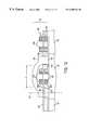
- FIG. 4shows a head gimbal assembly (HGA) according to the prior art.
- the head gimbal assemblyincludes a base 21 attached to a load beam 23 .
- the load beam 23includes an arm 20 attached between the base 21 and a suspension 22 .
- the suspension 22is attached to the arm 20 at a first end and is attached to a read/write head 24 at an opposite end.
- a pre-amp chip 142is attached to the base 21 .
- the pre-amp chip 142is electrically connected to the read/write head 24 by a metallic interconnection 144 such as copper traces or wires.
- the metallic interconnection 144carries electrical signals between the pre-amp chip 142 and the read/write head 24 .
- the pre-amp chip 142is connected to a controller connector 146 which can electrically connect the pre-amp chip to a controller (not shown).
- the pre amp-chip 142is also configured to pass electric signals to and from the controller.
- the pre-amp chip 142is located on the base 21 to place it close to the read/write head 24 . Shortening the distance between the pre-amp chip 142 and the read/write head 24 allows for a higher circuit resonant frequency, in turn allowing for higher data transfer rates. However, it is also necessary to match the impedance of the metallic interconnection 144 with the impedance of the read/write head 24 as failure to do so may degrade the signal. To match the impedance of prior art read/write heads 24 , a metallic interconnection 144 of the prior art has had to be sufficiently long, as impedance in a conductor increases as a function of its length. Consequently, this has necessitated placing the pre-amp chip 142 further away from the read/write head 24 than would otherwise be desirable.
- a write element with a lower impedancethat would allow a pre-amp chip to be located nearer to the write element and preferably on the load beam itself. Further, it is desired that fabrication of such a write element, and a read/write head incorporating the same, be inexpensive, quick, and simple.
- the present inventionprovides a magnetic recording device and method for making the same having a specifically tailored impedance to allow for a pre-amp chip to be located on the load beam nearer to the recording device than previously possible.
- a recording device for recording data on a magnetic mediumcomprises a yoke, a write gap layer, two coil layers, and three insulation layers.
- the yokehaving a characteristic yoke length, comprises a first pole, a second pole, a backgap portion, and a first pole pedestal, each formed of ferromagnetic materials.
- the first and second poleseach have a pole tip portion aligned with one another. Both poles are magnetically connected by way of the backgap portion, located distal their respective pole tip portions.
- the first pole pedestalis magnetically connected to, and aligned with, the first pole tip portion.
- Another embodimentis directed towards incorporating into the yoke a second pole pedestal, also formed of a ferromagnetic material, and situated between the write gap layer and the second pole.
- the yokeforms a discontinuous ring with a single gap.
- a write gap layerWithin the interior space defined by the yoke are a write gap layer, two coil layers, and three insulation layers.
- the write gap layerextends from the write gap region, the space between the first pole pedestal and the second pole tip portion, to the distal end of the second pole, and separates the turns of the first coil layer from the turns of the second coil layer.
- a first pole insulation layerinsulates the first pole from the turns of the first coil layer, and a first coil insulation layer disposed between the turns of the first coil layer insulates those turns from one another.
- a second coil insulation layerinsulates the turns of the second coil layer from each other and from the second pole.
- the write gap layer and each of the insulation layersmay be formed of suitable non-magnetic and electrically insulating materials, while the turns of the two coil layers may be formed of electrically conductive materials. At a minimum, each coil layer has at least one turn.
- This structureis advantageous because it allows for a shorter yoke length that reduces the device's flux rise time, thus, allowing for higher data recording rates.
- the placement of the write gap layeris also advantageous in this design because it limits the height of the first coil layer, thereby reducing the overall stack height of the device. Reducing the stack height facilitates the formation of the second pole.
- Another embodiment of the present inventionis a data transfer device for exchanging data with a magnetic medium comprising a load beam to which a recording device and a pre-amp chip are attached.
- the recording deviceis configured according to the embodiments previously described.
- the pre-amp chipis electrically connected to the recording device, and is connectable to a controller.
- the pre-amp chipis intended to pass electrical signals to and from both the controller and the recording device.
- Yet another embodimentis directed to locating the pre-amp chip at a sufficient distance from the recording device such that the impedance of the recording device and the impedance of a connector between the recording device and the pre-amp chip are substantially equal. Minimizing the impedance mismatch between the connector and the recording device while locating the pre-amp chip closer to the recording device is advantageous for decreasing the current rise time and the flux rise time, allowing for higher data transfer rates.
- Still other embodimentsinclude a read element, also connected to the pre-amp chip.
- a read elementmay include two shields and a read sensor, where the read sensor is disposed between a first shield and the first pole of the recording device configured to act as a second shield.
- a medium support and a read/write head support systemadditionally include a medium support and a read/write head support system.
- the medium supportmay further include a spindle on which the magnetic medium can be supported, and a medium motor capable of rotating the magnetic medium around the axis of the spindle.
- the read/write head support systemfurther includes the load beam and pre-amp chip, and is intended to suspend the read/write head proximate to the magnetic medium.
- a method for forming a recording deviceincludes providing a first pole having a pole tip portion.
- the first poleis substantially planarized prior to forming a first pole pedestal above and magnetically connected to the first pole at its pole tip portion.
- a backgap portionis formed above and magnetically connected to the first pole distal to its pole tip portion.
- a first pole insulation materialis deposited over the first pole pedestal, first pole, and backgap portion and a first pre-coil layer is formed above the first pole insulation layer.
- a first coil insulation layeris deposited over the first pre-coil layer and then substantially planarized to expose the first pole pedestal, first pre-coil layer, and backgap portion.
- a write gap layeris formed over the exposed first pole pedestal and first coil layer, and a second coil layer is formed above the write gap layer.
- a second coil insulation layeris formed over the second coil layer, and a second pole is formed over the write gap material and second coil insulation layer, and also over the backgap portion with which it is magnetically connected.
- FIG. 1Ais a partial cross-sectional elevation view of a magnetic data storage system
- FIG. 1Bis a top plan view along line 1 B— 1 B of FIG. 1A;
- FIG. 2is a cross-sectional view of a read/write head including a single coil layer according to the prior art
- FIG. 3is a cross-sectional view of a read/write head including two coil layers according to the prior art
- FIG. 4is a perspective view of a head gimbal assembly (HGA) according to the prior art
- FIG. 5is a cross sectional view of a read/write head according to an embodiment of the present invention.
- FIG. 6is an ABS view of a write element of the read/write head according to an embodiment of the present invention.
- FIGS. 7-12are cross-sectional views of a read/write head at various stages of fabrication, according to an embodiment of the present invention.
- FIG. 13is an ABS view of a write element of the read/write head according to another embodiment of the present invention.
- FIG. 14is a perspective view of a head gimbal assembly (HGA) according to an embodiment of the present invention.
- HGAhead gimbal assembly
- FIGS. 1A, 1 B, and 2 - 4were discussed with reference to the prior art.
- FIG. 5is a cross sectional view of a read/write head 70 of the present invention.
- the read/write head 70includes a read element 72 and a write element 74 . Both the read element 72 and write element 74 have surfaces that form part of an air bearing surface (ABS), in a plane 76 , which can be aligned to face the surface of a magnetic disk 16 (see FIGS. 1 A and 1 B).
- the read element 72includes a first shield 30 , an intermediate layer 78 , which functions as a second shield, and a read sensor 34 that is located within a dielectric medium 35 between the first shield 30 and the second shield 78 .
- the read sensor 34can be a magnetoresistive sensor, such as an AMR or GMR sensor.
- the first shield 30 and the second shield 78can be formed of a ferromagnetic material, such as a nickel iron (NiFe) alloy.
- the write element 74includes the intermediate layer 78 , which operates as a first pole, and a second pole 80 which is also formed of a ferromagnetic material, such as NiFe.
- the first pole 78 and the second pole 80are connected by a backgap portion 82 , located distal to the ABS, which is additionally formed of a ferromagnetic material, for example NiFe.
- a first pole pedestal 84is connected to a first pole tip portion 86 of the first pole 78 . Further, the first pole pedestal 84 is aligned with a second pole tip portion 88 .
- the first pole 78 , second pole 80 , first pole pedestal 84 , and backgap portion 82form a yoke 90 .
- the region of the write element 74which includes the first pole pedestal 84 , a first pole tip portion 86 , and a second pole tip portion 88 , is referred to as the yoke tip portion 92 .
- the yoke tip portion 92there is additionally a write gap 89 situated between the first pole pedestal 84 and the second pole tip region 88 .
- the write gap 89may be formed of any suitable electrically insulating, non-magnetic material such as Silicon dioxide (SiO 2 ).
- a first coil layer 94 , and a second coil layer 96are disposed between the first pole 78 and the second pole 80 .
- the first and second coil layers 94 , 96can include one or more coil turns 98 , 100 , respectively that are formed of an electrically conductive material, such as copper.
- the first coil layer 94can be electrically connected with the second coil layer 96 .
- Both the first coil layer 94 and the second coil layer 96are electrically insulated from the yoke 90 .
- the first coil layer 94is electrically insulated from the first pole 78 by a first pole insulation layer 102 .
- the first pole insulation layer 102extends from the first pole pedestal 84 to the backgap portion 82 , and can be formed of any suitable electrically insulating, non-magnetic material such as silicon dioxide (SiO 2 ) or alumina (Al 2 O 3 ).
- the first pole insulation layer 102can be relatively thin, for example in the range of about 0.1 micron to about 0.5 micron.
- first coil turns 98can be electrically connected in a spiral fashion as is know the art, they are transversely electrically insulated from adjacent other first coil turns 98 by a first coil insulation layer 104 .
- the first coil insulation layer 104can include discrete segments disposed between adjacent first coil turns 98 as well as between the first coil layer 94 and the backgap portion 82 , and between the first coil layer 94 and the first pole pedestal 84 .
- the first coil insulation layer 104can be formed of any suitable non-magnetic, electrically insulating material, for example alumina (Al 2 O 3 ).
- the first pole insulation layer 102also insulates the first coil layer 94 from the backgap portion 82 and the first pole pedestal 84 .
- the only insulation between the first coil layer 94 and the first pole pedestal 84may be the first coil insulation layer 104 , or alternatively the only insulation may be the first pole insulation layer 102 .
- the only insulation between the first coil layer 94 and the backgap portion 82may be the first coil insulation layer 104 , or alternatively the only insulation may be the first pole insulation layer 102 .
- a write gap layer 106is disposed above the first pole pedestal 84 , the first coil layer 94 and the first coil insulation layer 104 .
- the write gap layer 106can be formed of any suitable non-magnetic, electrically insulating material, such as alumina or silicon dioxide.
- the write gap layer 106may also be coextensive with the write gap 89 and electrically insulate the first coil layer 94 form the second coil layer 96 .
- a second coil insulation layer 108covers the second coil layer 96 , including between adjacent second coil turns 100 . In this way, the second coil insulation layer 108 provides electrical insulation between adjacent second coil turns 100 , and between the second coil layer 96 and the second pole 80 .
- the second coil insulation layer 108can be formed of any suitable non-magnetic, electrically insulating material, such as alumina, or cured photo resistive material, sometime referred to as “photoresist.”
- FIG. 6is an ABS view of a write element 74 of the read/write head 70 , according to an embodiment of the present invention.
- a width WP 1 P of an edge the first pole pedestal 84 at the ABSis narrower than the first pole tip portion 86 of the first pole 78 , and also narrower than the second pole tip portion 88 of the second pole 80 .
- the width WP 1 P of the edge of the first pole pedestal 84essentially defines the trackwidth for the write element 74 .
- the width of the edge of the first pole pedestal 84is in the range of about 0.2 micron to about 1.0 micron.
- FIGS. 7-12are cross-sectional views depicting the formation of the write element 74 at different stages of fabrication, according to another embodiment of the present invention.
- a first pole 78 surrounded by a build up layer 79is provided.
- the first polecan be formed of any suitable ferromagnetic material, such as NiFe.
- the build up layer 79can be formed of any suitable non magnetic, electrically insulating material, such as alumina.
- the first pole 78 and buildup layer 79can be planerized to form a substantially planer upper surface 114 .
- the planerizationcan be performed using known techniques such as chemical mechanical polishing (CMP), or any other technique that result in a surface 114 that is substantially planer.
- CMPchemical mechanical polishing
- a first pole pedestal 84 and a backgap portion 82are formed above and electrically connected to the first pole 78 .
- the first pole pedestal 84 and backgap portion 82can be formed by any suitable method, including various methods and techniques known to those skilled in the art.
- a first patterned plating maskcan be formed above the first pole 78 .
- Such a maskcan be formed, for example, by patterning photoresist as is well known in the art.
- a ferromagnetic materialcan then be plated over the first pole 78 with the first patterned plating mask in place.
- the ferromagnetic materialcan be any material having desirable magnetic properties, for example NiFe.
- the patterned plating maskis then removed, leaving the first pole pedestal 84 and back gap portion 82 above the first pole 78 . Also shown in FIG. 8, a first pole insulation material 116 is deposited over the first pole pedestal 84 and backgap portion 82 , as well as the first pole 78 .
- the first pole insulation materialcan be any suitable non-magnetic, electrically insulating material, such as silicon dioxide, and can be deposited using techniques well known in the art.
- FIG. 9depicts the formation of a first pre-coil layer 118 above the first pole insulation material 116 .
- the first pre-coil layer 118can include one or more first pre-coil turns 120 .
- the pre-coil turns 120can be spirally connected, as is well known in the art, i.e., each pre-coil turn 120 can be electrically connected in series with an adjacent pre-coil turn 120 .
- the first pre-coil turns 120can wind around the backgap portion 82 , with an inside portion Tin of the pre-coil turns 120 disposed between the first pole pedestal 84 and the backgap portion 82 , and an outside portion Tout of the first pre-coil turns 120 disposed on a side of the backgap portion 82 opposite from the first pole pedestal 84 .
- a single turn 120 aappears in cross section in FIG. 9 on opposite sides of the backgap portion 82 , as does another turn 120 b that is positioned within the first turn 120 a.
- the first pre-coil layercan be formed of any suitable electrically conductive material, such as copper.
- the first pre-coil layercan be formed using known methods, for example by platting. More specifically, a second patterned mask can be formed above the first pole insulation material 116 . A first electrically conductive material can then be plated over the first pole insulation material 116 with the second patterned plating mask in place. When the second patterned plating mask is removed, the first pre-coil layer remains above the first pole insulation layer 116 . Over the first pole insulation layer 116 and the first pre-coil layer 118 is deposited a first coil insulation layer material 122 .
- the first coil insulation materialcan be formed of any suitable non-magnetic electrically insulating material, such as alumina or silicon dioxide.
- the first coil insulation layer material 122 and the first pole insulation material 116are then substantially planerized to expose the first pole pedestal 84 , the backgap portion 82 , and the first pre-coil layer 118 , as is shown in FIG. 10 .
- This planerizationcan be performed by any known method, for example chemical mechanical polishing. Such planerization may be continued beyond simply exposing the first pole pedestal 84 , the backgap portion 82 , and the first pre-coil layer 118 , and may also include planerization of the first pole pedestal 84 , backgap portion 82 , and first pre-coil layer 118 themselves.
- first pre-coil layer 118forms a first coil layer 94 having one or more first coil turns 98 .
- first coil turns 98e.g., two first coil turns 98 are shown in FIG. 10 .
- This planerization processsubstantially defines the dimension of the first pole pedestal 84 , backgap portion 82 , and first coil layer 124 in the direction perpendicular to surface 114 .
- a write gap layer 106is formed over the exposed first pole pedestal 84 and the first coil layer 94 .
- the write gap material layer 106can be formed of any suitable non-magnetic, electrically insulating material, such as alumina.
- a second coil layer 96is then formed above the write gap layer 106 .
- the second coil layeris formed of any suitable electrically conductive material, such as copper, and includes one or more second coil turns 100 .
- the second coil layer 96can be formed using a variety of known methods and/or techniques. For example, a third patterned plating mask can be formed above the write gap layer 106 .
- a second electrically conductive materialcan then be plated above the write gap layer 106 with the third patterned plating mask in place.
- the second electrically conductive materialcan be the same or a different material than the first electrically conductive material, for example copper can be used.
- the third patterned plating maskcan then be removed, with the remaining second conductive material forming the second coil layer 96 .
- a second coil insulation layer 108shown in FIG. 12 is formed over a second coil layer 96 , including filling the spaces between adjacent second coil turns 100 .
- the second coil insulation layer 108can be formed of any suitable non magnetic, electrically insulating material, such as cured photoresist.
- a second pole 80is then formed over the write gap layer 106 , backgap portion 82 , and second coil insulation layer 108 .
- the second pole 80can be formed of any suitable ferromagnetic material, such as NiFe, and can be formed using any of a variety of known methods and techniques, for example, masking and plating.
- the formation of the read/write head 70can additionally include the formation of other elements, such as an overcoat layer above the second pole. Once the wafer level fabrication is complete, the read/write head 70 can be cut from the wafer and lapped to form an ABS in the plane 76 .
- the completed write element 74 shown in FIG. 12can include only a total of four coil turns while maintaining a yoke length YL of about 5 microns.
- additional coil turnscan be included in one or both of the first coil layer 94 , and the second coil layer 96 .
- a total of about 2 to about 15 coil turnscan be included, with even more coil turns being included if desired.
- the yoke length YL of the write element 74can be in the range of about 3 microns to about 35 microns.
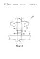
- FIG. 13shows another embodiment of the present invention in which a write element 130 can further include a second pole pedestal 132 electrically connected to the second pole tip portion 88 of the second pole 80 .
- the second pole pedestal 132can be formed of any suitable ferromagnetic material, such as NiFe.
- the write gap 89is defined between the first pole pedestal 84 , and the second pole pedestal 132 .
- a second pole pedestal 132can be formed above the write gap layer 106 before formation of the second pole 80 .
- the width WP 2 P of the second pole pedestal 132can be defined during plating of ferromagnetic material with a patterned plating mask.
- the width WP 2 Pcan be defined by etching or by ion milling.
- the width WP 1 P of the first pole pedestal 84can also be narrowed by ion milling.
- the first pole pedestal 84can be plated wider than the desired final width WP 1 P.
- the width WP 2 P of the second pole pedestal 132can be defined as substantially equal to the width WP 1 P of the first pole pedestal 84 .
- a second pole 80 of the write element 74 shown in FIG. 5can be formed with a second pole tip portion 88 that is narrower than the first pole pedestal 84 and the first pole tip portion 86 at the ABS.
- the track width of the write element 74is instead a function of the second pole tip portion 88 width at the ABS rather than the width WP 1 P of the edge of the first pole pedestal.
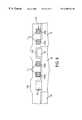
- FIG. 14shows a head gimbal assembly (HGA) which includes a base 21 attached to a load beam 23 .
- the load beam 23includes an arm 20 attached between the base 21 and a suspension 22 .
- the suspension 22is attached to the arm 20 at a first end and is attached to a read/write head 70 at an opposite end.
- a pre-amp chip 142is also located on the load beam 23 , for example on the arm 20 as shown in FIG. 14 .
- the pre-amp chip 142is electrically connected to the read/write head 70 via a metallic interconnection 144 .
- the metallic interconnection 144carries electrical signals between the pre-amp chip 142 and the read/write head 70 .
- the pre-amp chip 142is connected to a controller connector 146 that can electrically connect the pre-amp chip to a controller (not shown).
- the pre amp-chip 142is also configured to pass electric signals to and from the controller.
- the metallic interconnection 144can have a length L 2 that is shorter than the head connector length of the prior art (See FIG. 4 ), and preferably in the range of 10 mm to 20 mm. With this shorter length L 2 the impedance of the metallic interconnection 144 is reduced over the prior art.
- An advantage of the lower impedance in metallic interconnection 144is it further leads to a decrease in the current rise time of the recording current that is passed through the coil layers 94 and 96 . This reduction in current rise time further reduces the flux rise time at the write gap 89 . Thus, decreasing L 2 may lead to higher data recording rates.
- the configuration of the present inventioncan be used.
- the write element 70 of the present inventioncan be formed with a total of four coil turns which can cause the write element 74 to exhibit an impedance of about 3 nanohenrys (nh), substantially similar to the impedance of a head connector having a length L 2 .
- the yoke length YL of the write element 74can be shorter than if the total number of coil turns were included in a single coil layer.
- the yoke length YLcan be about 5 microns. This shorter yoke length YL further facilitates a shorter flux rise time than would be exhibited by a single coil layer of 4 turns. This further reduced flux rise time allows even higher data transfer rates to be achieved. For example, maximum data rates can be achieved of over about 2 gigabytes per second (Gb/s).
- the stack height SH of the write element 74is maintained substantially the same as a write element including only a single coil layer.
- the present inventionprovides structures and methods for providing a magnetic recording device with a chip on load-beam arrangement in which the impedance of the head connector is substantially similar to the impedance of the write element. This design allows for the pre-amp chip to be located closer to the recording device for higher data transfer rates.
Landscapes
- Engineering & Computer Science (AREA)
- Manufacturing & Machinery (AREA)
- Magnetic Heads (AREA)
Abstract
Description
Claims (16)
Priority Applications (1)
| Application Number | Priority Date | Filing Date | Title |
|---|---|---|---|
| US09/320,168US6400526B2 (en) | 1999-05-26 | 1999-05-26 | Advanced writer for chip-on-load beam |
Applications Claiming Priority (1)
| Application Number | Priority Date | Filing Date | Title |
|---|---|---|---|
| US09/320,168US6400526B2 (en) | 1999-05-26 | 1999-05-26 | Advanced writer for chip-on-load beam |
Publications (2)
| Publication Number | Publication Date |
|---|---|
| US20010012177A1 US20010012177A1 (en) | 2001-08-09 |
| US6400526B2true US6400526B2 (en) | 2002-06-04 |
Family
ID=23245181
Family Applications (1)
| Application Number | Title | Priority Date | Filing Date |
|---|---|---|---|
| US09/320,168Expired - Fee RelatedUS6400526B2 (en) | 1999-05-26 | 1999-05-26 | Advanced writer for chip-on-load beam |
Country Status (1)
| Country | Link |
|---|---|
| US (1) | US6400526B2 (en) |
Cited By (136)
| Publication number | Priority date | Publication date | Assignee | Title |
|---|---|---|---|---|
| US6587805B2 (en)* | 2000-02-25 | 2003-07-01 | Seagate Technology Llc | Testing a write transducer as a reader |
| US20030179498A1 (en)* | 2002-03-22 | 2003-09-25 | Hsiao Wen-Chein David | Magnetic head having a notched pole piece structure and method of making the same |
| US20040070872A1 (en)* | 2001-06-18 | 2004-04-15 | Hitachi Global Storage Technologies | High data rate write head |
| US20050024765A1 (en)* | 2003-08-01 | 2005-02-03 | Headway Technologies, Inc. | Method to make a planar writer with low D.C. coil resistance |
| US20060023351A1 (en)* | 2004-07-30 | 2006-02-02 | Hitachi Global Storage Technologies | Bilayer coil insulation for magnetic write heads to minimize pole recession |
| US20090015965A1 (en)* | 2007-07-11 | 2009-01-15 | Samsung Electronics Co., Ltd. | Perpendicular magnetic recording head and method for manufacturing the same |
| US8830628B1 (en) | 2009-02-23 | 2014-09-09 | Western Digital (Fremont), Llc | Method and system for providing a perpendicular magnetic recording head |
| US8879207B1 (en) | 2011-12-20 | 2014-11-04 | Western Digital (Fremont), Llc | Method for providing a side shield for a magnetic recording transducer using an air bridge |
| US8883017B1 (en) | 2013-03-12 | 2014-11-11 | Western Digital (Fremont), Llc | Method and system for providing a read transducer having seamless interfaces |
| US8917581B1 (en) | 2013-12-18 | 2014-12-23 | Western Digital Technologies, Inc. | Self-anneal process for a near field transducer and chimney in a hard disk drive assembly |
| US8923102B1 (en) | 2013-07-16 | 2014-12-30 | Western Digital (Fremont), Llc | Optical grating coupling for interferometric waveguides in heat assisted magnetic recording heads |
| US8947985B1 (en) | 2013-07-16 | 2015-02-03 | Western Digital (Fremont), Llc | Heat assisted magnetic recording transducers having a recessed pole |
| US8953422B1 (en) | 2014-06-10 | 2015-02-10 | Western Digital (Fremont), Llc | Near field transducer using dielectric waveguide core with fine ridge feature |
| US8958272B1 (en) | 2014-06-10 | 2015-02-17 | Western Digital (Fremont), Llc | Interfering near field transducer for energy assisted magnetic recording |
| US8971160B1 (en) | 2013-12-19 | 2015-03-03 | Western Digital (Fremont), Llc | Near field transducer with high refractive index pin for heat assisted magnetic recording |
| US8970988B1 (en) | 2013-12-31 | 2015-03-03 | Western Digital (Fremont), Llc | Electric gaps and method for making electric gaps for multiple sensor arrays |
| US8976635B1 (en) | 2014-06-10 | 2015-03-10 | Western Digital (Fremont), Llc | Near field transducer driven by a transverse electric waveguide for energy assisted magnetic recording |
| US8980109B1 (en) | 2012-12-11 | 2015-03-17 | Western Digital (Fremont), Llc | Method for providing a magnetic recording transducer using a combined main pole and side shield CMP for a wraparound shield scheme |
| US8982508B1 (en) | 2011-10-31 | 2015-03-17 | Western Digital (Fremont), Llc | Method for providing a side shield for a magnetic recording transducer |
| US8988812B1 (en) | 2013-11-27 | 2015-03-24 | Western Digital (Fremont), Llc | Multi-sensor array configuration for a two-dimensional magnetic recording (TDMR) operation |
| US8988825B1 (en) | 2014-02-28 | 2015-03-24 | Western Digital (Fremont, LLC | Method for fabricating a magnetic writer having half-side shields |
| US8984740B1 (en) | 2012-11-30 | 2015-03-24 | Western Digital (Fremont), Llc | Process for providing a magnetic recording transducer having a smooth magnetic seed layer |
| US8993217B1 (en) | 2013-04-04 | 2015-03-31 | Western Digital (Fremont), Llc | Double exposure technique for high resolution disk imaging |
| US8995087B1 (en) | 2006-11-29 | 2015-03-31 | Western Digital (Fremont), Llc | Perpendicular magnetic recording write head having a wrap around shield |
| US8997832B1 (en) | 2010-11-23 | 2015-04-07 | Western Digital (Fremont), Llc | Method of fabricating micrometer scale components |
| US9001467B1 (en) | 2014-03-05 | 2015-04-07 | Western Digital (Fremont), Llc | Method for fabricating side shields in a magnetic writer |
| US9001628B1 (en) | 2013-12-16 | 2015-04-07 | Western Digital (Fremont), Llc | Assistant waveguides for evaluating main waveguide coupling efficiency and diode laser alignment tolerances for hard disk |
| US9007725B1 (en) | 2014-10-07 | 2015-04-14 | Western Digital (Fremont), Llc | Sensor with positive coupling between dual ferromagnetic free layer laminates |
| US9007879B1 (en) | 2014-06-10 | 2015-04-14 | Western Digital (Fremont), Llc | Interfering near field transducer having a wide metal bar feature for energy assisted magnetic recording |
| US9007719B1 (en) | 2013-10-23 | 2015-04-14 | Western Digital (Fremont), Llc | Systems and methods for using double mask techniques to achieve very small features |
| US9013836B1 (en) | 2013-04-02 | 2015-04-21 | Western Digital (Fremont), Llc | Method and system for providing an antiferromagnetically coupled return pole |
| US9042051B2 (en) | 2013-08-15 | 2015-05-26 | Western Digital (Fremont), Llc | Gradient write gap for perpendicular magnetic recording writer |
| US9042208B1 (en) | 2013-03-11 | 2015-05-26 | Western Digital Technologies, Inc. | Disk drive measuring fly height by applying a bias voltage to an electrically insulated write component of a head |
| US9042057B1 (en) | 2013-01-09 | 2015-05-26 | Western Digital (Fremont), Llc | Methods for providing magnetic storage elements with high magneto-resistance using Heusler alloys |
| US9042058B1 (en) | 2013-10-17 | 2015-05-26 | Western Digital Technologies, Inc. | Shield designed for middle shields in a multiple sensor array |
| US9042052B1 (en) | 2014-06-23 | 2015-05-26 | Western Digital (Fremont), Llc | Magnetic writer having a partially shunted coil |
| US9053735B1 (en) | 2014-06-20 | 2015-06-09 | Western Digital (Fremont), Llc | Method for fabricating a magnetic writer using a full-film metal planarization |
| US9065043B1 (en) | 2012-06-29 | 2015-06-23 | Western Digital (Fremont), Llc | Tunnel magnetoresistance read head with narrow shield-to-shield spacing |
| US9064527B1 (en) | 2013-04-12 | 2015-06-23 | Western Digital (Fremont), Llc | High order tapered waveguide for use in a heat assisted magnetic recording head |
| US9064507B1 (en) | 2009-07-31 | 2015-06-23 | Western Digital (Fremont), Llc | Magnetic etch-stop layer for magnetoresistive read heads |
| US9064528B1 (en) | 2013-05-17 | 2015-06-23 | Western Digital Technologies, Inc. | Interferometric waveguide usable in shingled heat assisted magnetic recording in the absence of a near-field transducer |
| US9070381B1 (en) | 2013-04-12 | 2015-06-30 | Western Digital (Fremont), Llc | Magnetic recording read transducer having a laminated free layer |
| US9082423B1 (en) | 2013-12-18 | 2015-07-14 | Western Digital (Fremont), Llc | Magnetic recording write transducer having an improved trailing surface profile |
| US9087527B1 (en) | 2014-10-28 | 2015-07-21 | Western Digital (Fremont), Llc | Apparatus and method for middle shield connection in magnetic recording transducers |
| US9087534B1 (en) | 2011-12-20 | 2015-07-21 | Western Digital (Fremont), Llc | Method and system for providing a read transducer having soft and hard magnetic bias structures |
| US9093639B2 (en) | 2012-02-21 | 2015-07-28 | Western Digital (Fremont), Llc | Methods for manufacturing a magnetoresistive structure utilizing heating and cooling |
| US9104107B1 (en) | 2013-04-03 | 2015-08-11 | Western Digital (Fremont), Llc | DUV photoresist process |
| US9111550B1 (en) | 2014-12-04 | 2015-08-18 | Western Digital (Fremont), Llc | Write transducer having a magnetic buffer layer spaced between a side shield and a write pole by non-magnetic layers |
| US9111558B1 (en) | 2014-03-14 | 2015-08-18 | Western Digital (Fremont), Llc | System and method of diffractive focusing of light in a waveguide |
| US9111564B1 (en) | 2013-04-02 | 2015-08-18 | Western Digital (Fremont), Llc | Magnetic recording writer having a main pole with multiple flare angles |
| US9123362B1 (en) | 2011-03-22 | 2015-09-01 | Western Digital (Fremont), Llc | Methods for assembling an electrically assisted magnetic recording (EAMR) head |
| US9123358B1 (en) | 2012-06-11 | 2015-09-01 | Western Digital (Fremont), Llc | Conformal high moment side shield seed layer for perpendicular magnetic recording writer |
| US9123359B1 (en) | 2010-12-22 | 2015-09-01 | Western Digital (Fremont), Llc | Magnetic recording transducer with sputtered antiferromagnetic coupling trilayer between plated ferromagnetic shields and method of fabrication |
| US9123374B1 (en) | 2015-02-12 | 2015-09-01 | Western Digital (Fremont), Llc | Heat assisted magnetic recording writer having an integrated polarization rotation plate |
| US9135937B1 (en) | 2014-05-09 | 2015-09-15 | Western Digital (Fremont), Llc | Current modulation on laser diode for energy assisted magnetic recording transducer |
| US9135930B1 (en) | 2014-03-06 | 2015-09-15 | Western Digital (Fremont), Llc | Method for fabricating a magnetic write pole using vacuum deposition |
| US9142233B1 (en) | 2014-02-28 | 2015-09-22 | Western Digital (Fremont), Llc | Heat assisted magnetic recording writer having a recessed pole |
| US9147408B1 (en) | 2013-12-19 | 2015-09-29 | Western Digital (Fremont), Llc | Heated AFM layer deposition and cooling process for TMR magnetic recording sensor with high pinning field |
| US9147404B1 (en) | 2015-03-31 | 2015-09-29 | Western Digital (Fremont), Llc | Method and system for providing a read transducer having a dual free layer |
| US9153255B1 (en) | 2014-03-05 | 2015-10-06 | Western Digital (Fremont), Llc | Method for fabricating a magnetic writer having an asymmetric gap and shields |
| US9183854B2 (en) | 2014-02-24 | 2015-11-10 | Western Digital (Fremont), Llc | Method to make interferometric taper waveguide for HAMR light delivery |
| US9190085B1 (en) | 2014-03-12 | 2015-11-17 | Western Digital (Fremont), Llc | Waveguide with reflective grating for localized energy intensity |
| US9190079B1 (en) | 2014-09-22 | 2015-11-17 | Western Digital (Fremont), Llc | Magnetic write pole having engineered radius of curvature and chisel angle profiles |
| US9194692B1 (en) | 2013-12-06 | 2015-11-24 | Western Digital (Fremont), Llc | Systems and methods for using white light interferometry to measure undercut of a bi-layer structure |
| US9202480B2 (en) | 2009-10-14 | 2015-12-01 | Western Digital (Fremont), LLC. | Double patterning hard mask for damascene perpendicular magnetic recording (PMR) writer |
| US9202493B1 (en) | 2014-02-28 | 2015-12-01 | Western Digital (Fremont), Llc | Method of making an ultra-sharp tip mode converter for a HAMR head |
| US9214169B1 (en) | 2014-06-20 | 2015-12-15 | Western Digital (Fremont), Llc | Magnetic recording read transducer having a laminated free layer |
| US9214165B1 (en) | 2014-12-18 | 2015-12-15 | Western Digital (Fremont), Llc | Magnetic writer having a gradient in saturation magnetization of the shields |
| US9213322B1 (en) | 2012-08-16 | 2015-12-15 | Western Digital (Fremont), Llc | Methods for providing run to run process control using a dynamic tuner |
| US9214172B2 (en) | 2013-10-23 | 2015-12-15 | Western Digital (Fremont), Llc | Method of manufacturing a magnetic read head |
| US9230565B1 (en) | 2014-06-24 | 2016-01-05 | Western Digital (Fremont), Llc | Magnetic shield for magnetic recording head |
| US9236560B1 (en) | 2014-12-08 | 2016-01-12 | Western Digital (Fremont), Llc | Spin transfer torque tunneling magnetoresistive device having a laminated free layer with perpendicular magnetic anisotropy |
| US9245543B1 (en) | 2010-06-25 | 2016-01-26 | Western Digital (Fremont), Llc | Method for providing an energy assisted magnetic recording head having a laser integrally mounted to the slider |
| US9245562B1 (en) | 2015-03-30 | 2016-01-26 | Western Digital (Fremont), Llc | Magnetic recording writer with a composite main pole |
| US9245545B1 (en) | 2013-04-12 | 2016-01-26 | Wester Digital (Fremont), Llc | Short yoke length coils for magnetic heads in disk drives |
| US9251813B1 (en) | 2009-04-19 | 2016-02-02 | Western Digital (Fremont), Llc | Method of making a magnetic recording head |
| US9263067B1 (en) | 2013-05-29 | 2016-02-16 | Western Digital (Fremont), Llc | Process for making PMR writer with constant side wall angle |
| US9263071B1 (en) | 2015-03-31 | 2016-02-16 | Western Digital (Fremont), Llc | Flat NFT for heat assisted magnetic recording |
| US9269382B1 (en) | 2012-06-29 | 2016-02-23 | Western Digital (Fremont), Llc | Method and system for providing a read transducer having improved pinning of the pinned layer at higher recording densities |
| US9275657B1 (en) | 2013-08-14 | 2016-03-01 | Western Digital (Fremont), Llc | Process for making PMR writer with non-conformal side gaps |
| US9280990B1 (en) | 2013-12-11 | 2016-03-08 | Western Digital (Fremont), Llc | Method for fabricating a magnetic writer using multiple etches |
| US9287494B1 (en) | 2013-06-28 | 2016-03-15 | Western Digital (Fremont), Llc | Magnetic tunnel junction (MTJ) with a magnesium oxide tunnel barrier |
| US9286919B1 (en) | 2014-12-17 | 2016-03-15 | Western Digital (Fremont), Llc | Magnetic writer having a dual side gap |
| US9305583B1 (en) | 2014-02-18 | 2016-04-05 | Western Digital (Fremont), Llc | Method for fabricating a magnetic writer using multiple etches of damascene materials |
| US9312064B1 (en) | 2015-03-02 | 2016-04-12 | Western Digital (Fremont), Llc | Method to fabricate a magnetic head including ion milling of read gap using dual layer hard mask |
| US9318130B1 (en) | 2013-07-02 | 2016-04-19 | Western Digital (Fremont), Llc | Method to fabricate tunneling magnetic recording heads with extended pinned layer |
| US9336814B1 (en) | 2013-03-12 | 2016-05-10 | Western Digital (Fremont), Llc | Inverse tapered waveguide for use in a heat assisted magnetic recording head |
| US9343087B1 (en) | 2014-12-21 | 2016-05-17 | Western Digital (Fremont), Llc | Method for fabricating a magnetic writer having half shields |
| US9343098B1 (en) | 2013-08-23 | 2016-05-17 | Western Digital (Fremont), Llc | Method for providing a heat assisted magnetic recording transducer having protective pads |
| US9343086B1 (en) | 2013-09-11 | 2016-05-17 | Western Digital (Fremont), Llc | Magnetic recording write transducer having an improved sidewall angle profile |
| US9349392B1 (en) | 2012-05-24 | 2016-05-24 | Western Digital (Fremont), Llc | Methods for improving adhesion on dielectric substrates |
| US9349394B1 (en) | 2013-10-18 | 2016-05-24 | Western Digital (Fremont), Llc | Method for fabricating a magnetic writer having a gradient side gap |
| US9361913B1 (en) | 2013-06-03 | 2016-06-07 | Western Digital (Fremont), Llc | Recording read heads with a multi-layer AFM layer methods and apparatuses |
| US9361914B1 (en) | 2014-06-18 | 2016-06-07 | Western Digital (Fremont), Llc | Magnetic sensor with thin capping layer |
| US9368134B1 (en) | 2010-12-16 | 2016-06-14 | Western Digital (Fremont), Llc | Method and system for providing an antiferromagnetically coupled writer |
| US9384763B1 (en) | 2015-03-26 | 2016-07-05 | Western Digital (Fremont), Llc | Dual free layer magnetic reader having a rear bias structure including a soft bias layer |
| US9384765B1 (en) | 2015-09-24 | 2016-07-05 | Western Digital (Fremont), Llc | Method and system for providing a HAMR writer having improved optical efficiency |
| US9396742B1 (en) | 2012-11-30 | 2016-07-19 | Western Digital (Fremont), Llc | Magnetoresistive sensor for a magnetic storage system read head, and fabrication method thereof |
| US9396743B1 (en) | 2014-02-28 | 2016-07-19 | Western Digital (Fremont), Llc | Systems and methods for controlling soft bias thickness for tunnel magnetoresistance readers |
| US9406331B1 (en) | 2013-06-17 | 2016-08-02 | Western Digital (Fremont), Llc | Method for making ultra-narrow read sensor and read transducer device resulting therefrom |
| US9424866B1 (en) | 2015-09-24 | 2016-08-23 | Western Digital (Fremont), Llc | Heat assisted magnetic recording write apparatus having a dielectric gap |
| US9431038B1 (en) | 2015-06-29 | 2016-08-30 | Western Digital (Fremont), Llc | Method for fabricating a magnetic write pole having an improved sidewall angle profile |
| US9431031B1 (en) | 2015-03-24 | 2016-08-30 | Western Digital (Fremont), Llc | System and method for magnetic transducers having multiple sensors and AFC shields |
| US9431047B1 (en) | 2013-05-01 | 2016-08-30 | Western Digital (Fremont), Llc | Method for providing an improved AFM reader shield |
| US9431039B1 (en) | 2013-05-21 | 2016-08-30 | Western Digital (Fremont), Llc | Multiple sensor array usable in two-dimensional magnetic recording |
| US9431032B1 (en) | 2013-08-14 | 2016-08-30 | Western Digital (Fremont), Llc | Electrical connection arrangement for a multiple sensor array usable in two-dimensional magnetic recording |
| US9437251B1 (en) | 2014-12-22 | 2016-09-06 | Western Digital (Fremont), Llc | Apparatus and method having TDMR reader to reader shunts |
| US9443541B1 (en) | 2015-03-24 | 2016-09-13 | Western Digital (Fremont), Llc | Magnetic writer having a gradient in saturation magnetization of the shields and return pole |
| US9441938B1 (en) | 2013-10-08 | 2016-09-13 | Western Digital (Fremont), Llc | Test structures for measuring near field transducer disc length |
| US9449621B1 (en) | 2015-03-26 | 2016-09-20 | Western Digital (Fremont), Llc | Dual free layer magnetic reader having a rear bias structure having a high aspect ratio |
| US9449625B1 (en) | 2014-12-24 | 2016-09-20 | Western Digital (Fremont), Llc | Heat assisted magnetic recording head having a plurality of diffusion barrier layers |
| US9472216B1 (en) | 2015-09-23 | 2016-10-18 | Western Digital (Fremont), Llc | Differential dual free layer magnetic reader |
| US9484051B1 (en) | 2015-11-09 | 2016-11-01 | The Provost, Fellows, Foundation Scholars and the other members of Board, of the College of the Holy and Undivided Trinity of Queen Elizabeth near Dublin | Method and system for reducing undesirable reflections in a HAMR write apparatus |
| US9508363B1 (en) | 2014-06-17 | 2016-11-29 | Western Digital (Fremont), Llc | Method for fabricating a magnetic write pole having a leading edge bevel |
| US9508372B1 (en) | 2015-06-03 | 2016-11-29 | Western Digital (Fremont), Llc | Shingle magnetic writer having a low sidewall angle pole |
| US9508365B1 (en) | 2015-06-24 | 2016-11-29 | Western Digital (Fremont), LLC. | Magnetic reader having a crystal decoupling structure |
| US9530443B1 (en) | 2015-06-25 | 2016-12-27 | Western Digital (Fremont), Llc | Method for fabricating a magnetic recording device having a high aspect ratio structure |
| US9564150B1 (en) | 2015-11-24 | 2017-02-07 | Western Digital (Fremont), Llc | Magnetic read apparatus having an improved read sensor isolation circuit |
| US9595273B1 (en) | 2015-09-30 | 2017-03-14 | Western Digital (Fremont), Llc | Shingle magnetic writer having nonconformal shields |
| US9646639B2 (en) | 2015-06-26 | 2017-05-09 | Western Digital (Fremont), Llc | Heat assisted magnetic recording writer having integrated polarization rotation waveguides |
| US9666214B1 (en) | 2015-09-23 | 2017-05-30 | Western Digital (Fremont), Llc | Free layer magnetic reader that may have a reduced shield-to-shield spacing |
| US9721595B1 (en) | 2014-12-04 | 2017-08-01 | Western Digital (Fremont), Llc | Method for providing a storage device |
| US9741366B1 (en) | 2014-12-18 | 2017-08-22 | Western Digital (Fremont), Llc | Method for fabricating a magnetic writer having a gradient in saturation magnetization of the shields |
| US9740805B1 (en) | 2015-12-01 | 2017-08-22 | Western Digital (Fremont), Llc | Method and system for detecting hotspots for photolithographically-defined devices |
| US9754611B1 (en) | 2015-11-30 | 2017-09-05 | Western Digital (Fremont), Llc | Magnetic recording write apparatus having a stepped conformal trailing shield |
| US9767831B1 (en) | 2015-12-01 | 2017-09-19 | Western Digital (Fremont), Llc | Magnetic writer having convex trailing surface pole and conformal write gap |
| US9786301B1 (en) | 2014-12-02 | 2017-10-10 | Western Digital (Fremont), Llc | Apparatuses and methods for providing thin shields in a multiple sensor array |
| US9799351B1 (en) | 2015-11-30 | 2017-10-24 | Western Digital (Fremont), Llc | Short yoke length writer having assist coils |
| US9812155B1 (en) | 2015-11-23 | 2017-11-07 | Western Digital (Fremont), Llc | Method and system for fabricating high junction angle read sensors |
| US9842615B1 (en) | 2015-06-26 | 2017-12-12 | Western Digital (Fremont), Llc | Magnetic reader having a nonmagnetic insertion layer for the pinning layer |
| US9858951B1 (en) | 2015-12-01 | 2018-01-02 | Western Digital (Fremont), Llc | Method for providing a multilayer AFM layer in a read sensor |
| US9881638B1 (en) | 2014-12-17 | 2018-01-30 | Western Digital (Fremont), Llc | Method for providing a near-field transducer (NFT) for a heat assisted magnetic recording (HAMR) device |
| US9934811B1 (en) | 2014-03-07 | 2018-04-03 | Western Digital (Fremont), Llc | Methods for controlling stray fields of magnetic features using magneto-elastic anisotropy |
| US9953670B1 (en) | 2015-11-10 | 2018-04-24 | Western Digital (Fremont), Llc | Method and system for providing a HAMR writer including a multi-mode interference device |
| US10037770B1 (en) | 2015-11-12 | 2018-07-31 | Western Digital (Fremont), Llc | Method for providing a magnetic recording write apparatus having a seamless pole |
| US10074387B1 (en) | 2014-12-21 | 2018-09-11 | Western Digital (Fremont), Llc | Method and system for providing a read transducer having symmetric antiferromagnetically coupled shields |
Families Citing this family (2)
| Publication number | Priority date | Publication date | Assignee | Title |
|---|---|---|---|---|
| US20020191334A1 (en)* | 2001-06-18 | 2002-12-19 | Yimin Hsu | Magnetic transducer with pedestal pole piece structure |
| US8717136B2 (en)* | 2012-01-10 | 2014-05-06 | International Business Machines Corporation | Inductor with laminated yoke |
Citations (22)
| Publication number | Priority date | Publication date | Assignee | Title |
|---|---|---|---|---|
| US3891995A (en) | 1972-09-14 | 1975-06-24 | Hitachi Ltd | Magnetic head |
| US4052749A (en) | 1976-05-19 | 1977-10-04 | Matsushita Electric Industrial Co., Ltd. | Thin film magnetic head |
| SU705509A1 (en)* | 1978-06-05 | 1979-12-25 | Предприятие П/Я А-3759 | Magnetic head |
| US4241367A (en) | 1978-03-03 | 1980-12-23 | Matsushita Electric Industrial Co., Ltd. | Thin film magnetic head |
| US4318148A (en) | 1979-07-04 | 1982-03-02 | Matsushita Electric Industrial Co., Ltd. | Thin-film magnetic head |
| US4416056A (en) | 1977-12-13 | 1983-11-22 | Fujitsu Limited | Process for preparation of film coils |
| US4458279A (en) | 1981-03-23 | 1984-07-03 | Magnex Corporation | Thin film transducer and method of making same |
| JPS59195314A (en)* | 1983-04-21 | 1984-11-06 | Sony Corp | Thin film magnetic head |
| US4490760A (en) | 1981-01-23 | 1984-12-25 | Matsushita Electric Industrial Co., Ltd. | Thin-film magnetic head |
| US4884157A (en) | 1987-07-28 | 1989-11-28 | Applied Magnetics Corporation | Thin film magnetic head with coil windings receiving trench |
| US5173826A (en) | 1991-06-03 | 1992-12-22 | Read-Rite Corp. | Thin film head with coils of varying thickness |
| JPH0546935A (en)* | 1991-08-12 | 1993-02-26 | Alps Electric Co Ltd | Thin film magnetic head |
| US5668689A (en) | 1994-03-03 | 1997-09-16 | Seagate Technology, Inc. | Inverted magnetoresistive head |
| US5694276A (en) | 1996-07-01 | 1997-12-02 | Read-Rite Corporation | Shielded magnetic head having an inductive coil with low mutual inductance |
| US5699605A (en) | 1994-05-23 | 1997-12-23 | Seagate Technology, Inc. | Method for forming a magnetic thin film head with recessed basecoat |
| US5734534A (en) | 1993-12-29 | 1998-03-31 | Sony Corporation | Magnetic head |
| US5796564A (en) | 1994-05-09 | 1998-08-18 | Sony Corporation | Magnetic head having a recessed portion corresponding to a magnetic path and method of manufacturing the same |
| US6034848A (en)* | 1998-04-22 | 2000-03-07 | International Business Machines Corporation | Low profile multi-layer coil merged thin film magnetic head |
| US6055138A (en)* | 1998-05-06 | 2000-04-25 | Read-Rite Corporation | Thin film pedestal pole tips write head having narrower lower pedestal pole tip |
| US6105238A (en)* | 1997-12-04 | 2000-08-22 | Matsushita-Kotobukie Electronics Industries, Ltd. | Method and structure for defining track width on a recording head |
| US6191918B1 (en)* | 1998-10-23 | 2001-02-20 | International Business Machines Corporation | Embedded dual coil planar structure |
| US6317288B1 (en)* | 1998-08-28 | 2001-11-13 | Tdk Corporation | Thin-film magnetic head and method of manufacturing same |
- 1999
- 1999-05-26USUS09/320,168patent/US6400526B2/ennot_activeExpired - Fee Related
Patent Citations (22)
| Publication number | Priority date | Publication date | Assignee | Title |
|---|---|---|---|---|
| US3891995A (en) | 1972-09-14 | 1975-06-24 | Hitachi Ltd | Magnetic head |
| US4052749A (en) | 1976-05-19 | 1977-10-04 | Matsushita Electric Industrial Co., Ltd. | Thin film magnetic head |
| US4416056A (en) | 1977-12-13 | 1983-11-22 | Fujitsu Limited | Process for preparation of film coils |
| US4241367A (en) | 1978-03-03 | 1980-12-23 | Matsushita Electric Industrial Co., Ltd. | Thin film magnetic head |
| SU705509A1 (en)* | 1978-06-05 | 1979-12-25 | Предприятие П/Я А-3759 | Magnetic head |
| US4318148A (en) | 1979-07-04 | 1982-03-02 | Matsushita Electric Industrial Co., Ltd. | Thin-film magnetic head |
| US4490760A (en) | 1981-01-23 | 1984-12-25 | Matsushita Electric Industrial Co., Ltd. | Thin-film magnetic head |
| US4458279A (en) | 1981-03-23 | 1984-07-03 | Magnex Corporation | Thin film transducer and method of making same |
| JPS59195314A (en)* | 1983-04-21 | 1984-11-06 | Sony Corp | Thin film magnetic head |
| US4884157A (en) | 1987-07-28 | 1989-11-28 | Applied Magnetics Corporation | Thin film magnetic head with coil windings receiving trench |
| US5173826A (en) | 1991-06-03 | 1992-12-22 | Read-Rite Corp. | Thin film head with coils of varying thickness |
| JPH0546935A (en)* | 1991-08-12 | 1993-02-26 | Alps Electric Co Ltd | Thin film magnetic head |
| US5734534A (en) | 1993-12-29 | 1998-03-31 | Sony Corporation | Magnetic head |
| US5668689A (en) | 1994-03-03 | 1997-09-16 | Seagate Technology, Inc. | Inverted magnetoresistive head |
| US5796564A (en) | 1994-05-09 | 1998-08-18 | Sony Corporation | Magnetic head having a recessed portion corresponding to a magnetic path and method of manufacturing the same |
| US5699605A (en) | 1994-05-23 | 1997-12-23 | Seagate Technology, Inc. | Method for forming a magnetic thin film head with recessed basecoat |
| US5694276A (en) | 1996-07-01 | 1997-12-02 | Read-Rite Corporation | Shielded magnetic head having an inductive coil with low mutual inductance |
| US6105238A (en)* | 1997-12-04 | 2000-08-22 | Matsushita-Kotobukie Electronics Industries, Ltd. | Method and structure for defining track width on a recording head |
| US6034848A (en)* | 1998-04-22 | 2000-03-07 | International Business Machines Corporation | Low profile multi-layer coil merged thin film magnetic head |
| US6055138A (en)* | 1998-05-06 | 2000-04-25 | Read-Rite Corporation | Thin film pedestal pole tips write head having narrower lower pedestal pole tip |
| US6317288B1 (en)* | 1998-08-28 | 2001-11-13 | Tdk Corporation | Thin-film magnetic head and method of manufacturing same |
| US6191918B1 (en)* | 1998-10-23 | 2001-02-20 | International Business Machines Corporation | Embedded dual coil planar structure |
Cited By (158)
| Publication number | Priority date | Publication date | Assignee | Title |
|---|---|---|---|---|
| US6587805B2 (en)* | 2000-02-25 | 2003-07-01 | Seagate Technology Llc | Testing a write transducer as a reader |
| US6952326B2 (en)* | 2001-06-18 | 2005-10-04 | Hitachi Global Storage Technologies Netherlands B.V. | High data rate write head |
| US20040070872A1 (en)* | 2001-06-18 | 2004-04-15 | Hitachi Global Storage Technologies | High data rate write head |
| US7489474B2 (en)* | 2002-03-22 | 2009-02-10 | International Business Machines Corporation | Magnetic head having a notched pole piece structure |
| US20030179498A1 (en)* | 2002-03-22 | 2003-09-25 | Hsiao Wen-Chein David | Magnetic head having a notched pole piece structure and method of making the same |
| US6947255B2 (en)* | 2002-03-22 | 2005-09-20 | International Business Machines Corporation | Magnetic head having a notched pole piece structure and method of making the same |
| US20050024765A1 (en)* | 2003-08-01 | 2005-02-03 | Headway Technologies, Inc. | Method to make a planar writer with low D.C. coil resistance |
| US7038880B2 (en) | 2003-08-01 | 2006-05-02 | Headway Technologies, Inc. | Method to make a planar writer with low D.C. coil resistance |
| US20060023351A1 (en)* | 2004-07-30 | 2006-02-02 | Hitachi Global Storage Technologies | Bilayer coil insulation for magnetic write heads to minimize pole recession |
| US7292408B2 (en)* | 2004-07-30 | 2007-11-06 | Hitachi Global Storage Technologies Netherlands B.V. | Bilayer coil insulation for magnetic write heads to minimize pole recession |
| US8995087B1 (en) | 2006-11-29 | 2015-03-31 | Western Digital (Fremont), Llc | Perpendicular magnetic recording write head having a wrap around shield |
| US20090015965A1 (en)* | 2007-07-11 | 2009-01-15 | Samsung Electronics Co., Ltd. | Perpendicular magnetic recording head and method for manufacturing the same |
| US8035921B2 (en)* | 2007-07-11 | 2011-10-11 | Samsung Electronics Co., Ltd. | Perpendicular magnetic recording head and method for manufacturing the same |
| US8830628B1 (en) | 2009-02-23 | 2014-09-09 | Western Digital (Fremont), Llc | Method and system for providing a perpendicular magnetic recording head |
| US9251813B1 (en) | 2009-04-19 | 2016-02-02 | Western Digital (Fremont), Llc | Method of making a magnetic recording head |
| US9064507B1 (en) | 2009-07-31 | 2015-06-23 | Western Digital (Fremont), Llc | Magnetic etch-stop layer for magnetoresistive read heads |
| US9202480B2 (en) | 2009-10-14 | 2015-12-01 | Western Digital (Fremont), LLC. | Double patterning hard mask for damascene perpendicular magnetic recording (PMR) writer |
| US9245543B1 (en) | 2010-06-25 | 2016-01-26 | Western Digital (Fremont), Llc | Method for providing an energy assisted magnetic recording head having a laser integrally mounted to the slider |
| US8997832B1 (en) | 2010-11-23 | 2015-04-07 | Western Digital (Fremont), Llc | Method of fabricating micrometer scale components |
| US9159345B1 (en) | 2010-11-23 | 2015-10-13 | Western Digital (Fremont), Llc | Micrometer scale components |
| US9672847B2 (en) | 2010-11-23 | 2017-06-06 | Western Digital (Fremont), Llc | Micrometer scale components |
| US9368134B1 (en) | 2010-12-16 | 2016-06-14 | Western Digital (Fremont), Llc | Method and system for providing an antiferromagnetically coupled writer |
| US9123359B1 (en) | 2010-12-22 | 2015-09-01 | Western Digital (Fremont), Llc | Magnetic recording transducer with sputtered antiferromagnetic coupling trilayer between plated ferromagnetic shields and method of fabrication |
| US9123362B1 (en) | 2011-03-22 | 2015-09-01 | Western Digital (Fremont), Llc | Methods for assembling an electrically assisted magnetic recording (EAMR) head |
| US8982508B1 (en) | 2011-10-31 | 2015-03-17 | Western Digital (Fremont), Llc | Method for providing a side shield for a magnetic recording transducer |
| US9087534B1 (en) | 2011-12-20 | 2015-07-21 | Western Digital (Fremont), Llc | Method and system for providing a read transducer having soft and hard magnetic bias structures |
| US8879207B1 (en) | 2011-12-20 | 2014-11-04 | Western Digital (Fremont), Llc | Method for providing a side shield for a magnetic recording transducer using an air bridge |
| US9093639B2 (en) | 2012-02-21 | 2015-07-28 | Western Digital (Fremont), Llc | Methods for manufacturing a magnetoresistive structure utilizing heating and cooling |
| US9349392B1 (en) | 2012-05-24 | 2016-05-24 | Western Digital (Fremont), Llc | Methods for improving adhesion on dielectric substrates |
| US9940950B2 (en) | 2012-05-24 | 2018-04-10 | Western Digital (Fremont), Llc | Methods for improving adhesion on dielectric substrates |
| US9123358B1 (en) | 2012-06-11 | 2015-09-01 | Western Digital (Fremont), Llc | Conformal high moment side shield seed layer for perpendicular magnetic recording writer |
| US9065043B1 (en) | 2012-06-29 | 2015-06-23 | Western Digital (Fremont), Llc | Tunnel magnetoresistance read head with narrow shield-to-shield spacing |
| US9269382B1 (en) | 2012-06-29 | 2016-02-23 | Western Digital (Fremont), Llc | Method and system for providing a read transducer having improved pinning of the pinned layer at higher recording densities |
| US9412400B2 (en) | 2012-06-29 | 2016-08-09 | Western Digital (Fremont), Llc | Tunnel magnetoresistance read head with narrow shield-to-shield spacing |
| US9213322B1 (en) | 2012-08-16 | 2015-12-15 | Western Digital (Fremont), Llc | Methods for providing run to run process control using a dynamic tuner |
| US9396742B1 (en) | 2012-11-30 | 2016-07-19 | Western Digital (Fremont), Llc | Magnetoresistive sensor for a magnetic storage system read head, and fabrication method thereof |
| US8984740B1 (en) | 2012-11-30 | 2015-03-24 | Western Digital (Fremont), Llc | Process for providing a magnetic recording transducer having a smooth magnetic seed layer |
| US8980109B1 (en) | 2012-12-11 | 2015-03-17 | Western Digital (Fremont), Llc | Method for providing a magnetic recording transducer using a combined main pole and side shield CMP for a wraparound shield scheme |
| US9042057B1 (en) | 2013-01-09 | 2015-05-26 | Western Digital (Fremont), Llc | Methods for providing magnetic storage elements with high magneto-resistance using Heusler alloys |
| US9042208B1 (en) | 2013-03-11 | 2015-05-26 | Western Digital Technologies, Inc. | Disk drive measuring fly height by applying a bias voltage to an electrically insulated write component of a head |
| US9336814B1 (en) | 2013-03-12 | 2016-05-10 | Western Digital (Fremont), Llc | Inverse tapered waveguide for use in a heat assisted magnetic recording head |
| US8883017B1 (en) | 2013-03-12 | 2014-11-11 | Western Digital (Fremont), Llc | Method and system for providing a read transducer having seamless interfaces |
| US9111564B1 (en) | 2013-04-02 | 2015-08-18 | Western Digital (Fremont), Llc | Magnetic recording writer having a main pole with multiple flare angles |
| US9013836B1 (en) | 2013-04-02 | 2015-04-21 | Western Digital (Fremont), Llc | Method and system for providing an antiferromagnetically coupled return pole |
| US9104107B1 (en) | 2013-04-03 | 2015-08-11 | Western Digital (Fremont), Llc | DUV photoresist process |
| US8993217B1 (en) | 2013-04-04 | 2015-03-31 | Western Digital (Fremont), Llc | Double exposure technique for high resolution disk imaging |
| US9064527B1 (en) | 2013-04-12 | 2015-06-23 | Western Digital (Fremont), Llc | High order tapered waveguide for use in a heat assisted magnetic recording head |
| US9070381B1 (en) | 2013-04-12 | 2015-06-30 | Western Digital (Fremont), Llc | Magnetic recording read transducer having a laminated free layer |
| US9245545B1 (en) | 2013-04-12 | 2016-01-26 | Wester Digital (Fremont), Llc | Short yoke length coils for magnetic heads in disk drives |
| US9431047B1 (en) | 2013-05-01 | 2016-08-30 | Western Digital (Fremont), Llc | Method for providing an improved AFM reader shield |
| US9064528B1 (en) | 2013-05-17 | 2015-06-23 | Western Digital Technologies, Inc. | Interferometric waveguide usable in shingled heat assisted magnetic recording in the absence of a near-field transducer |
| US9431039B1 (en) | 2013-05-21 | 2016-08-30 | Western Digital (Fremont), Llc | Multiple sensor array usable in two-dimensional magnetic recording |
| US9263067B1 (en) | 2013-05-29 | 2016-02-16 | Western Digital (Fremont), Llc | Process for making PMR writer with constant side wall angle |
| US9361913B1 (en) | 2013-06-03 | 2016-06-07 | Western Digital (Fremont), Llc | Recording read heads with a multi-layer AFM layer methods and apparatuses |
| US9406331B1 (en) | 2013-06-17 | 2016-08-02 | Western Digital (Fremont), Llc | Method for making ultra-narrow read sensor and read transducer device resulting therefrom |
| US9287494B1 (en) | 2013-06-28 | 2016-03-15 | Western Digital (Fremont), Llc | Magnetic tunnel junction (MTJ) with a magnesium oxide tunnel barrier |
| US9318130B1 (en) | 2013-07-02 | 2016-04-19 | Western Digital (Fremont), Llc | Method to fabricate tunneling magnetic recording heads with extended pinned layer |
| US8947985B1 (en) | 2013-07-16 | 2015-02-03 | Western Digital (Fremont), Llc | Heat assisted magnetic recording transducers having a recessed pole |
| US8923102B1 (en) | 2013-07-16 | 2014-12-30 | Western Digital (Fremont), Llc | Optical grating coupling for interferometric waveguides in heat assisted magnetic recording heads |
| US9431032B1 (en) | 2013-08-14 | 2016-08-30 | Western Digital (Fremont), Llc | Electrical connection arrangement for a multiple sensor array usable in two-dimensional magnetic recording |
| US9275657B1 (en) | 2013-08-14 | 2016-03-01 | Western Digital (Fremont), Llc | Process for making PMR writer with non-conformal side gaps |
| US9042051B2 (en) | 2013-08-15 | 2015-05-26 | Western Digital (Fremont), Llc | Gradient write gap for perpendicular magnetic recording writer |
| US9343098B1 (en) | 2013-08-23 | 2016-05-17 | Western Digital (Fremont), Llc | Method for providing a heat assisted magnetic recording transducer having protective pads |
| US9343086B1 (en) | 2013-09-11 | 2016-05-17 | Western Digital (Fremont), Llc | Magnetic recording write transducer having an improved sidewall angle profile |
| US9441938B1 (en) | 2013-10-08 | 2016-09-13 | Western Digital (Fremont), Llc | Test structures for measuring near field transducer disc length |
| US9042058B1 (en) | 2013-10-17 | 2015-05-26 | Western Digital Technologies, Inc. | Shield designed for middle shields in a multiple sensor array |
| US9349394B1 (en) | 2013-10-18 | 2016-05-24 | Western Digital (Fremont), Llc | Method for fabricating a magnetic writer having a gradient side gap |
| US9830936B2 (en) | 2013-10-23 | 2017-11-28 | Western Digital (Fremont), Llc | Magnetic read head with antiferromagentic layer |
| US9007719B1 (en) | 2013-10-23 | 2015-04-14 | Western Digital (Fremont), Llc | Systems and methods for using double mask techniques to achieve very small features |
| US9214172B2 (en) | 2013-10-23 | 2015-12-15 | Western Digital (Fremont), Llc | Method of manufacturing a magnetic read head |
| US8988812B1 (en) | 2013-11-27 | 2015-03-24 | Western Digital (Fremont), Llc | Multi-sensor array configuration for a two-dimensional magnetic recording (TDMR) operation |
| US9194692B1 (en) | 2013-12-06 | 2015-11-24 | Western Digital (Fremont), Llc | Systems and methods for using white light interferometry to measure undercut of a bi-layer structure |
| US9280990B1 (en) | 2013-12-11 | 2016-03-08 | Western Digital (Fremont), Llc | Method for fabricating a magnetic writer using multiple etches |
| US9001628B1 (en) | 2013-12-16 | 2015-04-07 | Western Digital (Fremont), Llc | Assistant waveguides for evaluating main waveguide coupling efficiency and diode laser alignment tolerances for hard disk |
| US8917581B1 (en) | 2013-12-18 | 2014-12-23 | Western Digital Technologies, Inc. | Self-anneal process for a near field transducer and chimney in a hard disk drive assembly |
| US9082423B1 (en) | 2013-12-18 | 2015-07-14 | Western Digital (Fremont), Llc | Magnetic recording write transducer having an improved trailing surface profile |
| US9147408B1 (en) | 2013-12-19 | 2015-09-29 | Western Digital (Fremont), Llc | Heated AFM layer deposition and cooling process for TMR magnetic recording sensor with high pinning field |
| US8971160B1 (en) | 2013-12-19 | 2015-03-03 | Western Digital (Fremont), Llc | Near field transducer with high refractive index pin for heat assisted magnetic recording |
| US8970988B1 (en) | 2013-12-31 | 2015-03-03 | Western Digital (Fremont), Llc | Electric gaps and method for making electric gaps for multiple sensor arrays |
| US9305583B1 (en) | 2014-02-18 | 2016-04-05 | Western Digital (Fremont), Llc | Method for fabricating a magnetic writer using multiple etches of damascene materials |
| US9183854B2 (en) | 2014-02-24 | 2015-11-10 | Western Digital (Fremont), Llc | Method to make interferometric taper waveguide for HAMR light delivery |
| US9396743B1 (en) | 2014-02-28 | 2016-07-19 | Western Digital (Fremont), Llc | Systems and methods for controlling soft bias thickness for tunnel magnetoresistance readers |
| US9202493B1 (en) | 2014-02-28 | 2015-12-01 | Western Digital (Fremont), Llc | Method of making an ultra-sharp tip mode converter for a HAMR head |
| US8988825B1 (en) | 2014-02-28 | 2015-03-24 | Western Digital (Fremont, LLC | Method for fabricating a magnetic writer having half-side shields |
| US9142233B1 (en) | 2014-02-28 | 2015-09-22 | Western Digital (Fremont), Llc | Heat assisted magnetic recording writer having a recessed pole |
| US9001467B1 (en) | 2014-03-05 | 2015-04-07 | Western Digital (Fremont), Llc | Method for fabricating side shields in a magnetic writer |
| US9153255B1 (en) | 2014-03-05 | 2015-10-06 | Western Digital (Fremont), Llc | Method for fabricating a magnetic writer having an asymmetric gap and shields |
| US9349393B2 (en) | 2014-03-05 | 2016-05-24 | Western Digital (Fremont), Llc | Magnetic writer having an asymmetric gap and shields |
| US9135930B1 (en) | 2014-03-06 | 2015-09-15 | Western Digital (Fremont), Llc | Method for fabricating a magnetic write pole using vacuum deposition |
| US9934811B1 (en) | 2014-03-07 | 2018-04-03 | Western Digital (Fremont), Llc | Methods for controlling stray fields of magnetic features using magneto-elastic anisotropy |
| US9190085B1 (en) | 2014-03-12 | 2015-11-17 | Western Digital (Fremont), Llc | Waveguide with reflective grating for localized energy intensity |
| US9495984B2 (en) | 2014-03-12 | 2016-11-15 | Western Digital (Fremont), Llc | Waveguide with reflective grating for localized energy intensity |
| US9111558B1 (en) | 2014-03-14 | 2015-08-18 | Western Digital (Fremont), Llc | System and method of diffractive focusing of light in a waveguide |
| US9135937B1 (en) | 2014-05-09 | 2015-09-15 | Western Digital (Fremont), Llc | Current modulation on laser diode for energy assisted magnetic recording transducer |
| US8976635B1 (en) | 2014-06-10 | 2015-03-10 | Western Digital (Fremont), Llc | Near field transducer driven by a transverse electric waveguide for energy assisted magnetic recording |
| US9311952B2 (en) | 2014-06-10 | 2016-04-12 | Western Digital (Fremont), Llc | Interfering near field transducer for energy assisted magnetic recording |
| US9159346B1 (en) | 2014-06-10 | 2015-10-13 | Western Digital (Fremont), Llc | Near field transducer using dielectric waveguide core with fine ridge feature |
| US8958272B1 (en) | 2014-06-10 | 2015-02-17 | Western Digital (Fremont), Llc | Interfering near field transducer for energy assisted magnetic recording |
| US8953422B1 (en) | 2014-06-10 | 2015-02-10 | Western Digital (Fremont), Llc | Near field transducer using dielectric waveguide core with fine ridge feature |
| US9007879B1 (en) | 2014-06-10 | 2015-04-14 | Western Digital (Fremont), Llc | Interfering near field transducer having a wide metal bar feature for energy assisted magnetic recording |
| US9508363B1 (en) | 2014-06-17 | 2016-11-29 | Western Digital (Fremont), Llc | Method for fabricating a magnetic write pole having a leading edge bevel |
| US9361914B1 (en) | 2014-06-18 | 2016-06-07 | Western Digital (Fremont), Llc | Magnetic sensor with thin capping layer |
| US9214169B1 (en) | 2014-06-20 | 2015-12-15 | Western Digital (Fremont), Llc | Magnetic recording read transducer having a laminated free layer |
| US9053735B1 (en) | 2014-06-20 | 2015-06-09 | Western Digital (Fremont), Llc | Method for fabricating a magnetic writer using a full-film metal planarization |
| US9042052B1 (en) | 2014-06-23 | 2015-05-26 | Western Digital (Fremont), Llc | Magnetic writer having a partially shunted coil |
| US9230565B1 (en) | 2014-06-24 | 2016-01-05 | Western Digital (Fremont), Llc | Magnetic shield for magnetic recording head |
| US9190079B1 (en) | 2014-09-22 | 2015-11-17 | Western Digital (Fremont), Llc | Magnetic write pole having engineered radius of curvature and chisel angle profiles |
| US9007725B1 (en) | 2014-10-07 | 2015-04-14 | Western Digital (Fremont), Llc | Sensor with positive coupling between dual ferromagnetic free layer laminates |
| US9087527B1 (en) | 2014-10-28 | 2015-07-21 | Western Digital (Fremont), Llc | Apparatus and method for middle shield connection in magnetic recording transducers |
| US9786301B1 (en) | 2014-12-02 | 2017-10-10 | Western Digital (Fremont), Llc | Apparatuses and methods for providing thin shields in a multiple sensor array |
| US9721595B1 (en) | 2014-12-04 | 2017-08-01 | Western Digital (Fremont), Llc | Method for providing a storage device |
| US9111550B1 (en) | 2014-12-04 | 2015-08-18 | Western Digital (Fremont), Llc | Write transducer having a magnetic buffer layer spaced between a side shield and a write pole by non-magnetic layers |
| US9705072B2 (en) | 2014-12-08 | 2017-07-11 | Western Digital (Fremont), Llc | Spin transfer torque tunneling magnetoresistive device having a laminated free layer with perpendicular magnetic anisotropy |
| US9236560B1 (en) | 2014-12-08 | 2016-01-12 | Western Digital (Fremont), Llc | Spin transfer torque tunneling magnetoresistive device having a laminated free layer with perpendicular magnetic anisotropy |
| US10553241B2 (en) | 2014-12-17 | 2020-02-04 | Western Digital Technologies, Inc. | Near-field transducer (NFT) for a heat assisted magnetic recording (HAMR) device |
| US9881638B1 (en) | 2014-12-17 | 2018-01-30 | Western Digital (Fremont), Llc | Method for providing a near-field transducer (NFT) for a heat assisted magnetic recording (HAMR) device |
| US9286919B1 (en) | 2014-12-17 | 2016-03-15 | Western Digital (Fremont), Llc | Magnetic writer having a dual side gap |
| US9214165B1 (en) | 2014-12-18 | 2015-12-15 | Western Digital (Fremont), Llc | Magnetic writer having a gradient in saturation magnetization of the shields |
| US9741366B1 (en) | 2014-12-18 | 2017-08-22 | Western Digital (Fremont), Llc | Method for fabricating a magnetic writer having a gradient in saturation magnetization of the shields |
| US10074387B1 (en) | 2014-12-21 | 2018-09-11 | Western Digital (Fremont), Llc | Method and system for providing a read transducer having symmetric antiferromagnetically coupled shields |
| US9343087B1 (en) | 2014-12-21 | 2016-05-17 | Western Digital (Fremont), Llc | Method for fabricating a magnetic writer having half shields |
| US9437251B1 (en) | 2014-12-22 | 2016-09-06 | Western Digital (Fremont), Llc | Apparatus and method having TDMR reader to reader shunts |
| US9449625B1 (en) | 2014-12-24 | 2016-09-20 | Western Digital (Fremont), Llc | Heat assisted magnetic recording head having a plurality of diffusion barrier layers |
| US9123374B1 (en) | 2015-02-12 | 2015-09-01 | Western Digital (Fremont), Llc | Heat assisted magnetic recording writer having an integrated polarization rotation plate |
| US9312064B1 (en) | 2015-03-02 | 2016-04-12 | Western Digital (Fremont), Llc | Method to fabricate a magnetic head including ion milling of read gap using dual layer hard mask |
| US9431031B1 (en) | 2015-03-24 | 2016-08-30 | Western Digital (Fremont), Llc | System and method for magnetic transducers having multiple sensors and AFC shields |
| US9443541B1 (en) | 2015-03-24 | 2016-09-13 | Western Digital (Fremont), Llc | Magnetic writer having a gradient in saturation magnetization of the shields and return pole |
| US9449621B1 (en) | 2015-03-26 | 2016-09-20 | Western Digital (Fremont), Llc | Dual free layer magnetic reader having a rear bias structure having a high aspect ratio |
| US9922672B1 (en) | 2015-03-26 | 2018-03-20 | Western Digital (Fremont), Llc | Dual free layer magnetic reader having a rear bias structure having a high aspect ratio |
| US9384763B1 (en) | 2015-03-26 | 2016-07-05 | Western Digital (Fremont), Llc | Dual free layer magnetic reader having a rear bias structure including a soft bias layer |
| US9245562B1 (en) | 2015-03-30 | 2016-01-26 | Western Digital (Fremont), Llc | Magnetic recording writer with a composite main pole |
| US9147404B1 (en) | 2015-03-31 | 2015-09-29 | Western Digital (Fremont), Llc | Method and system for providing a read transducer having a dual free layer |
| US9263071B1 (en) | 2015-03-31 | 2016-02-16 | Western Digital (Fremont), Llc | Flat NFT for heat assisted magnetic recording |
| US9508372B1 (en) | 2015-06-03 | 2016-11-29 | Western Digital (Fremont), Llc | Shingle magnetic writer having a low sidewall angle pole |
| US9508365B1 (en) | 2015-06-24 | 2016-11-29 | Western Digital (Fremont), LLC. | Magnetic reader having a crystal decoupling structure |
| US9530443B1 (en) | 2015-06-25 | 2016-12-27 | Western Digital (Fremont), Llc | Method for fabricating a magnetic recording device having a high aspect ratio structure |
| US9646639B2 (en) | 2015-06-26 | 2017-05-09 | Western Digital (Fremont), Llc | Heat assisted magnetic recording writer having integrated polarization rotation waveguides |
| US10242700B2 (en) | 2015-06-26 | 2019-03-26 | Western Digital (Fremont), Llc | Magnetic reader having a nonmagnetic insertion layer for the pinning layer |
| US9842615B1 (en) | 2015-06-26 | 2017-12-12 | Western Digital (Fremont), Llc | Magnetic reader having a nonmagnetic insertion layer for the pinning layer |
| US9431038B1 (en) | 2015-06-29 | 2016-08-30 | Western Digital (Fremont), Llc | Method for fabricating a magnetic write pole having an improved sidewall angle profile |
| US9472216B1 (en) | 2015-09-23 | 2016-10-18 | Western Digital (Fremont), Llc | Differential dual free layer magnetic reader |
| US9666214B1 (en) | 2015-09-23 | 2017-05-30 | Western Digital (Fremont), Llc | Free layer magnetic reader that may have a reduced shield-to-shield spacing |
| US9424866B1 (en) | 2015-09-24 | 2016-08-23 | Western Digital (Fremont), Llc | Heat assisted magnetic recording write apparatus having a dielectric gap |
| US9384765B1 (en) | 2015-09-24 | 2016-07-05 | Western Digital (Fremont), Llc | Method and system for providing a HAMR writer having improved optical efficiency |
| US9595273B1 (en) | 2015-09-30 | 2017-03-14 | Western Digital (Fremont), Llc | Shingle magnetic writer having nonconformal shields |
| US9484051B1 (en) | 2015-11-09 | 2016-11-01 | The Provost, Fellows, Foundation Scholars and the other members of Board, of the College of the Holy and Undivided Trinity of Queen Elizabeth near Dublin | Method and system for reducing undesirable reflections in a HAMR write apparatus |
| US10381029B2 (en) | 2015-11-10 | 2019-08-13 | Western Digital (Fremont), Llc | Method and system for providing a HAMR writer including a multi-mode interference device |
| US9953670B1 (en) | 2015-11-10 | 2018-04-24 | Western Digital (Fremont), Llc | Method and system for providing a HAMR writer including a multi-mode interference device |
| US10037770B1 (en) | 2015-11-12 | 2018-07-31 | Western Digital (Fremont), Llc | Method for providing a magnetic recording write apparatus having a seamless pole |
| US9812155B1 (en) | 2015-11-23 | 2017-11-07 | Western Digital (Fremont), Llc | Method and system for fabricating high junction angle read sensors |
| US9564150B1 (en) | 2015-11-24 | 2017-02-07 | Western Digital (Fremont), Llc | Magnetic read apparatus having an improved read sensor isolation circuit |
| US10121495B2 (en) | 2015-11-30 | 2018-11-06 | Western Digital (Fremont), Llc | Magnetic recording write apparatus having a stepped conformal trailing shield |
| US9799351B1 (en) | 2015-11-30 | 2017-10-24 | Western Digital (Fremont), Llc | Short yoke length writer having assist coils |
| US9754611B1 (en) | 2015-11-30 | 2017-09-05 | Western Digital (Fremont), Llc | Magnetic recording write apparatus having a stepped conformal trailing shield |
| US9997177B2 (en) | 2015-12-01 | 2018-06-12 | Western Digital (Fremont), Llc | Magnetic writer having convex trailing surface pole and conformal write gap |
| US9858951B1 (en) | 2015-12-01 | 2018-01-02 | Western Digital (Fremont), Llc | Method for providing a multilayer AFM layer in a read sensor |
| US9740805B1 (en) | 2015-12-01 | 2017-08-22 | Western Digital (Fremont), Llc | Method and system for detecting hotspots for photolithographically-defined devices |
| US9767831B1 (en) | 2015-12-01 | 2017-09-19 | Western Digital (Fremont), Llc | Magnetic writer having convex trailing surface pole and conformal write gap |
Also Published As
| Publication number | Publication date |
|---|---|
| US20010012177A1 (en) | 2001-08-09 |
Similar Documents
| Publication | Publication Date | Title |
|---|---|---|
| US6400526B2 (en) | Advanced writer for chip-on-load beam | |
| US6417998B1 (en) | Ultra small advanced write transducer and method for making same | |
| US6552874B1 (en) | Shared pole magnetic read-write head for achieving optimized erase band width and method of fabricating the same | |
| US6178070B1 (en) | Magnetic write head and method for making same | |
| US6483662B1 (en) | High density multi-coil magnetic write head having a reduced yoke length and short flux rise time | |
| US6304414B1 (en) | Thin film magnetic write head having an ultra-low stack height | |
| US6466404B1 (en) | Magnetic read/write device with insulated coil layer recessed into pole | |
| US6466402B1 (en) | Compact MR write structure | |
| US6282056B1 (en) | Tapered stitch pole writer for high density magnetic recording | |
| US7193815B1 (en) | Shielded pole magnetic head for perpendicular recording | |
| US6650503B1 (en) | Inductive write head including a thin high moment pedestal having a tapered edge | |
| US6381095B1 (en) | High performance thin film magnetic write element having high Bsat poles and method for making same | |
| JP2614412B2 (en) | Magnetic transducer / suspension assembly and manufacturing method, and magnetic disk drive system | |
| US6496330B1 (en) | Magnetic write head having a splitcoil structure | |
| US6396660B1 (en) | Magnetic write element having a thermally dissipative structure | |
| US7117583B2 (en) | Method and apparatus using a pre-patterned seed layer for providing an aligned coil for an inductive head structure | |
| US6693769B2 (en) | High data rate write head | |
| US7190552B2 (en) | Magnetic head having a damascene-fabricated write coil structure with coil layers extending between the poles for reduced electrical resistance | |
| US7119987B2 (en) | Thin-film magnetic head, a head gimbal assembly, and a hard disk drive | |
| US6785953B2 (en) | Process of fabricating a write head with protection of a second pole tip thickness | |
| JPH11283215A (en) | Thin film magnetic head and its production | |
| JP2667374B2 (en) | Method of manufacturing thin film magnetic transducer for magnetic disk storage system | |
| US7336445B2 (en) | Conductive stud for magnetic recording devices and method of making the same | |
| US20050007697A1 (en) | Magnetic transducer with pedestal pole piece structure | |
| US5694276A (en) | Shielded magnetic head having an inductive coil with low mutual inductance |
Legal Events
| Date | Code | Title | Description |
|---|---|---|---|
| AS | Assignment | Owner name:READ-RITE CORPORATION, CALIFORNIA Free format text:ASSIGNMENT OF ASSIGNORS INTEREST;ASSIGNORS:CRUE, JR., BILL W.;SHI, ZHUPEI;CORONA, CARLOS;AND OTHERS;REEL/FRAME:010120/0715;SIGNING DATES FROM 19990706 TO 19990712 | |
| AS | Assignment | Owner name:TENNENBAUM CAPITAL PARTNERS, LLC, CALIFORNIA Free format text:SECURITY INTEREST;ASSIGNOR:READ-RITE CORPORATION;REEL/FRAME:013616/0399 Effective date:20021224 | |
| AS | Assignment | Owner name:WESTERN DIGITAL (FREMONT), INC., CALIFORNIA Free format text:ASSIGNMENT OF ASSIGNORS INTEREST;ASSIGNOR:READ-RITE CORPORATION;REEL/FRAME:014506/0765 Effective date:20030731 | |
| AS | Assignment | Owner name:READ-RITE CORPORATION, CALIFORNIA Free format text:RELEASE OF SECURITY INTEREST;ASSIGNOR:TENNENBAUM CAPITAL PARTNERS, LLC;REEL/FRAME:014499/0476 Effective date:20030731 | |
| AS | Assignment | Owner name:GENERAL ELECTRIC CAPITAL CORPORATION, AS AGENT, CA Free format text:SECURITY INTEREST;ASSIGNORS:WESTERN DIGITAL TECHNOLOGIES, INC.;WESTERN DIGITAL (FREMONT), INC.;REEL/FRAME:014830/0957 Effective date:20030919 | |
| FPAY | Fee payment | Year of fee payment:4 | |
| AS | Assignment | Owner name:WESTERN DIGITAL TECHNOLOGIES, INC., CALIFORNIA Free format text:RELEASE BY SECURED PARTY;ASSIGNOR:GENERAL ELECTRIC CAPITAL CORPORATION, AS AGENT;REEL/FRAME:020599/0489 Effective date:20070809 Owner name:WESTERN DIGITAL (FREMONT), INC., CALIFORNIA Free format text:RELEASE BY SECURED PARTY;ASSIGNOR:GENERAL ELECTRIC CAPITAL CORPORATION, AS AGENT;REEL/FRAME:020599/0489 Effective date:20070809 | |
| FPAY | Fee payment | Year of fee payment:8 | |
| REMI | Maintenance fee reminder mailed | ||
| LAPS | Lapse for failure to pay maintenance fees | ||
| STCH | Information on status: patent discontinuation | Free format text:PATENT EXPIRED DUE TO NONPAYMENT OF MAINTENANCE FEES UNDER 37 CFR 1.362 | |
| FP | Lapsed due to failure to pay maintenance fee | Effective date:20140604 | |
| AS | Assignment | Owner name:WESTERN DIGITAL TECHNOLOGIES, INC., CALIFORNIA Free format text:ASSIGNMENT OF ASSIGNORS INTEREST;ASSIGNOR:WESTERN DIGITAL (FREMONT), LLC;REEL/FRAME:050450/0582 Effective date:20190508 |