US6399476B2 - Multilayer passivation process for forming air gaps within a dielectric between interconnections - Google Patents
Multilayer passivation process for forming air gaps within a dielectric between interconnectionsDownload PDFInfo
- Publication number
- US6399476B2 US6399476B2US09/432,101US43210199AUS6399476B2US 6399476 B2US6399476 B2US 6399476B2US 43210199 AUS43210199 AUS 43210199AUS 6399476 B2US6399476 B2US 6399476B2
- Authority
- US
- United States
- Prior art keywords
- layer
- spaced apart
- interconnections
- dielectric layer
- dielectric
- Prior art date
- Legal status (The legal status is an assumption and is not a legal conclusion. Google has not performed a legal analysis and makes no representation as to the accuracy of the status listed.)
- Expired - Lifetime
Links
Images


Classifications
- H—ELECTRICITY
- H01—ELECTRIC ELEMENTS
- H01L—SEMICONDUCTOR DEVICES NOT COVERED BY CLASS H10
- H01L21/00—Processes or apparatus adapted for the manufacture or treatment of semiconductor or solid state devices or of parts thereof
- H01L21/70—Manufacture or treatment of devices consisting of a plurality of solid state components formed in or on a common substrate or of parts thereof; Manufacture of integrated circuit devices or of parts thereof
- H01L21/71—Manufacture of specific parts of devices defined in group H01L21/70
- H01L21/768—Applying interconnections to be used for carrying current between separate components within a device comprising conductors and dielectrics
- H01L21/76801—Applying interconnections to be used for carrying current between separate components within a device comprising conductors and dielectrics characterised by the formation and the after-treatment of the dielectrics, e.g. smoothing
- H01L21/7682—Applying interconnections to be used for carrying current between separate components within a device comprising conductors and dielectrics characterised by the formation and the after-treatment of the dielectrics, e.g. smoothing the dielectric comprising air gaps
- H—ELECTRICITY
- H01—ELECTRIC ELEMENTS
- H01L—SEMICONDUCTOR DEVICES NOT COVERED BY CLASS H10
- H01L21/00—Processes or apparatus adapted for the manufacture or treatment of semiconductor or solid state devices or of parts thereof
- H01L21/02—Manufacture or treatment of semiconductor devices or of parts thereof
- H01L21/04—Manufacture or treatment of semiconductor devices or of parts thereof the devices having potential barriers, e.g. a PN junction, depletion layer or carrier concentration layer
- H01L21/18—Manufacture or treatment of semiconductor devices or of parts thereof the devices having potential barriers, e.g. a PN junction, depletion layer or carrier concentration layer the devices having semiconductor bodies comprising elements of Group IV of the Periodic Table or AIIIBV compounds with or without impurities, e.g. doping materials
- H01L21/30—Treatment of semiconductor bodies using processes or apparatus not provided for in groups H01L21/20 - H01L21/26
- H01L21/31—Treatment of semiconductor bodies using processes or apparatus not provided for in groups H01L21/20 - H01L21/26 to form insulating layers thereon, e.g. for masking or by using photolithographic techniques; After treatment of these layers; Selection of materials for these layers
- H01L21/3205—Deposition of non-insulating-, e.g. conductive- or resistive-, layers on insulating layers; After-treatment of these layers
Definitions
- the present inventionrelates generally to the fabrication of a semiconductor device, and more particularly to a multilayer dielectric process for forming air gaps therein for reducing permittivity of the dielectric between interconnections.
- semiconductor devicesare formed by alternating an insulating layer and a conductor in a predetermined manner over a silicon semiconductor substrate.
- the conductor separated by the insulating layeris electrically connected to overlying and underlying another conductors through openings (contact hole or via) in the insulating layers.
- Such conductorsmay include impurity diffusion region and metal line made of Al (aluminium), Ti (titanium), Ta (tantalum), W (tungsten), polycrystalline silicon, or a combination thereof.
- Interconnection linesare fashioned on the semiconductor device structure and spaced by a dielectric above an underlying conductor or substrate by a dielectric thickness. Each conductor is spaced a distance from other conductors by a dielectric within the same level of conductors. Accordingly, conductor-to-conductor capacitance (i.e., coupling capacitance) is generated. As circuit density increases, spacing between conductors decreases and thus coupling capacitance therebetween increases.
- the capacitance between conductorsis highly dependent on the insulator, or dielectric, used to separate them. Therefore it is required to reduce the permittivity of a dielectric material between conductors. As such, it would be desirable to employ a fabrication technique in which dielectrics between conductors achieve low permittivity.
- the lowest possible, or ideal, dielectric constantis 1.0, which is the dielectric constant of a vacuum, whereas air has a dielectric constant of less than 1.001.
- the present inventionwas made in view of the above problem, and the present invention is directed toward providing a multilayer dielectric process for forming air gaps within the dielectric between the interconnections for a low permittivity dielectric.
- the present inventionuses multilayer dielectric to purposely form air gaps within the dielectric.
- the permittivity of air within the dielectric materialis less than that of the surrounding dielectric material which allows an overall decrease in permittivity between interconnections and a corresponding increase in operation speed.
- the air gapsare formed by the multilayer dielectric process. More specifically, a first dielectric layer such as PE-CVD (plasma enhanced chemical vapor deposition) oxide layer using TEOS (tetraethyl orthosilicate) source is deposited on the patterned spaced metal interconnections.
- PE-CVD TEOS oxide layeris deposited to provide a poor step coverage over the interconnections, i.e., deposited relatively thickly at top sides and deposited relatively thinly at bottom sides of the patterned metal interconnections. This poor step coverage of first dielectric makes it easier to form the air gaps in subsequent second dielectric and serves to increase volume of the air gaps.
- the second dielectric layeris deposited over the first dielectric in such controlled manner that causes air gaps within the second dielectric.
- This second dielectric layerpreferably includes a low permittivity dielectric such as a silicon oxynitride(SiON) layer. This low permittivity advantageously reduces coupling capacitance between the patterned spaced metal lines and overlying other conductors.
- a method for forming air gaps in the dielectrics between the interconnectionsincludes providing at least a pair of spaced interconnects over a semiconductor topology.
- the semiconductor topologyincludes an interlayer insulating layer at a top thereof.
- the methodfurther includes depositing a first dielectric layer on the spaced interconnects and over the semiconductor substrate.
- the first dielectric layeris deposited relatively more thickly at top sides of the interconnects than at bottom sides of the interconnects.
- the first dielectric layeris made of an TEOS oxide layer by a PE-CVD technique.
- the methodfurther includes depositing a second dielectric layer over the first dielectric layer to cause the formation of an air gap in the second dielectric layer and between the spaced interconnects.
- the second dielectric layercan be made of silicon oxynitride.
- the second dielectric layermay be made of silicon nitride (SiN).
- the methodfurther includes depositing a third dielectric layer on the second dielectric layer.
- the methodfurther includes depositing a silicon nitride layer over the first dielectric layer, wherein the second dielectric layer is deposited thereover to cause the formation of the air gap.
- a method for forming air gaps in the dielectrics between the interconnectsincludes forming first metal patterns over a semiconductor substrate.
- the methodfurther includes forming an intermetal oxide layer over the first metal patterns to a thickness of about 0.8 microns.
- the methodfurther includes forming second spaced apart metal patterns over the intermetal oxide layer.
- the second spaced apart metal patternsare separated from each other by about 0.8 microns to 0.9 microns and have a height of about 0.15 microns.
- the methodfurther includes depositing a first passivation layer of an oxide on the second metal pattern to a thickness of about 0.15 microns.
- the first passivation layer of an oxideis deposited thickly at a top side of the second metal pattern and is deposited thinly at a bottom side of the second metal pattern.
- the methodfurther includes depositing a second passivation layer of silicon oxynitride to a thickness of about 1.2 microns, causing the formation of an air gap therein between the second metal patterns.
- the air gaphas a size of about 0.46 microns.
- the methodfurther includes depositing a third passivation layer of a polyimide to a thickness of about 10 microns over the second passivation layer of silicon oxynitride.
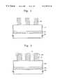
- FIG. 1is a partial cross-sectional view of an integrated circuit topography having an insulating layer and patterned metal interconnection structures according to the present invention
- FIG. 2illustrates a process step subsequent to that shown in FIG. 1 wherein a first passivation layer is deposited over the patterned metal interconnection structure;
- FIG. 3illustrates a process step subsequent to that shown in FIG. 2 wherein a second passivation layer is deposited over the first insulating layer and air gaps are formed therein;
- FIG. 4illustrates a process step subsequent to that shown in FIG. 3 wherein a third passivation layer is deposited over the second insulating layer;
- FIG. 5illustrates a cross-sectional view of a semiconductor substrate having an air gap using a PE-TEOS layer, silicon nitride layer, and silicon oxynitride layer in accordance with another embodiment of the present invention.
- the present inventionrelates to a method for forming air gaps in an insulating layer between the interconnections with the use of multilayer dielectric.
- the air gaps in the dielectric between interconnections (or conductors)reduces the coupling capacitance.
- FIG. 1schematically shows a cross-sectional view of an integrated circuit topology having an insulating layer 104 and patterned spaced conductors 106 .
- the conductors 106can be any spaced conductive pattern, for example, can be metal interconnections.
- the height of the conductors 106is about 1 microns to 1.2 microns and the distance between the conductors 106 can be about 0.8 microns to 0.9 microns.
- the ratio of pattern distance and pattern heightcan be about 0.8 ⁇ 0.9: 1.0 ⁇ 1.2.
- a first layer 108 of the multilayer dielectricis formed over the integrated circuit topology. This first layer is preferably selected as a material which has a poor step coverage.
- PE-CVDplasma enhanced chemical vapor deposition
- TEOSi.e., tetraethylorthosilicate [Si(OC 2 H 5 ) 4 ]
- Si(OC 2 H 5 ) 4tetraethylorthosilicate
- the PE-TEOS layer 108can be deposited to a thickness of about 0.15 microns. The deposition of this PE-TEOS layer 108 is carefully controlled such that the PE-TEOS layer 108 is deposited thickly at the top portion, especially the top sides (see dotted circle portion in FIG. 2) of the conductors 106 and deposited thinly at the bottom sides of the conductors 102 .
- a void 110is formed between the conductors 106 which has a relatively narrow opening size as compared to the size of its bottom. Such a void profile makes it easier to form desired air gaps, having a low dielectric permittivity of 1.001, between the conductors 106 . Furthermore, the thin PE-TEOS layer 108 on the bottom sides of the conductors 106 serves to increase the volume of the air gaps. Next, a second layer 112 of the multilayer dielectric is deposited to form the air gaps 114 therein between the conductors as shown in FIG. 3 .
- the second layer 112 of the multilayer dielectricis preferably selected from an insulating layer exhibiting a relatively low dielectric constant, such as a silicon oxynitride layer (SiON) and is deposited to a thickness more than 1 microns, preferably 1.2 microns, so as to form the air gaps 114 .
- the dielectric constant of the SiONis about 3.5.
- the air gaps 114are initiated during the deposition of the thin first dielectric 108 and completed during the deposition of the thick second dielectric 112 .
- the air gapspreferably each have a diameter of about 0.46 microns.
- a silicon nitride layer(SiN) can be used instead of the silicon oxynitride layer.
- SiNsilicon nitride layer
- a silicon nitride layer and a silicon oxynitride layermay be sequentially deposited over the PE-TEOS layer 108 with a thickness of about 0.6 microns and 1.0 microns, respectively. The presence of the air gaps 114 in the dielectric 112 between the conductors reduces the coupling capacitance and thereby reduce RC delay and accelerates device operation speed.
- the method for forming air gaps in the dielectric between conductorscan be preferably employed in the process of passivation for metal interconnections.
- the passivation process for metal interconnectionswill now be described with reference to FIGS. 1 to 4 .
- FIGS. 1 to 3will be cited again to this embodiment.
- the formation of the device isolation layer, transistors, bit line, capacitors, and other device elements which are not directively related to the formation of the air gapsare not shown and their explanation is omitted.
- an intermetal dielectric layer 104is formed over a semiconductor substrate.
- the intermetal dielectric layer 104may be a PE-CVD oxide layer, using TEOS source, or a FOX layer using inorganic spin-on-glass technique, and has a thickness more than 0.8 microns.
- a first metal interconnection 102has been formed by the conventional method below the intermetal dielectric layer 104 .
- a second layer of metalis deposited over the intermetal dielectric layer 104 by a conventional sputtering method.
- a photoresist layer(not shown) is spin coated over the second metal layer and patterned into desired configuration.
- the second metal layeris then anisotropically dry etched to form second spaced metal interconnections 106 using the patterned photoresist layer.
- the second metalis preferably made of aluminum and has a thickness of about 0.8 microns to 1.0 microns.
- a capping layer(not shown) such as Ti/TiN is formed between the intermetal dielectric layer 104 and the aluminium layer 106 , and on the aluminum layer 106 .
- the overall thickness of the second metal interconnectionis about 1 microns to 1.2 microns and the distance between the interconnections is about 0.8 microns to 0.9 microns.
- the patterned photoresist layeris then removed through conventional process such as O 2 plasma ashing and a subsequent stripping process.
- a first passivation layer 108is deposited over the second metal interconnections 106 .
- This first passivation layer 108serves to prevent the reaction between the metal interconnections and subsequent second passivation layer 112 .
- the first passivation layer 108is preferably made of a PE-CVD oxide layer using a TEOS source gas and deposited to a thickness of about 0.15 microns.
- another PECVD oxide layermay be used, such as a silane(SiH 4 ) based oxide layer.
- the PE-CVD silane based oxide layeris formed by using SiH 4 of about 115 sccm and N 2 O of about 1,700 sccm at a pressure of about 2.2 torr, and at a temperature about 400° C. for about 10 seconds.
- This PE-CVD oxide layerexhibits such a poor step coverage that it is deposited thickly at the top portion, specifically top sides of the second metal interconnections, while being deposited very thin at the bottom sides thereof.
- This poor step coverageallows easier formation of a void 110 between interconnections 106 which has a relatively narrow opening size as compared to the bottom size.
- This void 110 profilemakes it easier to form air gaps in subsequent process.
- the second passivation layer 112is deposited over the first passivation layer 104 to a thickness condition that forms air gaps 114 therein.
- the thickness of the second passivation layer 112is large enough, at least 1 microns, preferably more than 1.2 microns.
- the second passivation layeris made of a silicon oxynitride layer.
- This silicon oxynitride layeris formed by CVD (chemical vapor deposition) using about 280 sccm SiH 4 , about 8,000 sccm N 2 , about 300 sccm NH 3 , and about 300 sccm N 2 O at a pressure of about 2.6 torr, at a temperature about 390° C. for about 8 to 9 minutes.
- CVDchemical vapor deposition
- formed air gaps 114each have a diameter of about 0.46 microns.
- a silicon oxynitride layer with dielectric constant about 3.5is used.
- silicon nitride layermay be used instead, and the combination of silicon oxynitride and silicon nitride is also possible.
- This silicon nitride layeris formed by the CVD (chemical vapor deposition) method using about 400 sccm SiH 4 , about 2,300 sccm N 2 , and about 1,700 sccm NH 3 at a pressure of about 2.4 torr, and at a temperature of about 390° C. for about 30 to 40 seconds.
- a third conventional passivation layer 116such as a polyimide layer, is deposited over the resulting structure to a thickness of about 10 microns.
- the third passivation layer 116is then planarized and a conventional photography process is conducted and a metal contact pad (not shown) is formed in the third passivation layer 116 to the selected second metal interconnections. Subsequently, a process for forming other metal interconnections is further carried out.
- FIG. 5shows a cross-sectional view of a semiconductor topology according to another embodiment of the present invention.
- air gapsfor example an air gap 114
- a silicon nitride layer 109is formed to a thickness of about 0.6 microns.
- the silicon oxynitride layer 112is formed thickly so as to form the air gap 114 , for example, to a thickness of about 1.0 microns.
- the air gapsare formed in the dielectric layer by depositing a plurality of dielectric layers.
- Silicon oxynitride layer with a dielectric permittivity of about 3.5is preferentially selected as a second dielectric layer since the silicon oxynitride layer not only forms air gaps therein between the same level metal interconnections, but also reduces coupling capacitance between different level metal interconnections.
- the first dielectric layer formed on the conductive patternis deposited such that it provides a poor step coverage, deposited thickly at the top edge portion and deposited thinly at the bottom edge portion of the conductive pattern. The poor step coverage of the first dielectric layer makes it easier to form the air gaps in the second dielectric layer.
Landscapes
- Engineering & Computer Science (AREA)
- Physics & Mathematics (AREA)
- Condensed Matter Physics & Semiconductors (AREA)
- General Physics & Mathematics (AREA)
- Manufacturing & Machinery (AREA)
- Computer Hardware Design (AREA)
- Microelectronics & Electronic Packaging (AREA)
- Power Engineering (AREA)
- Internal Circuitry In Semiconductor Integrated Circuit Devices (AREA)
- Formation Of Insulating Films (AREA)
Abstract
Description
Claims (11)
Applications Claiming Priority (2)
| Application Number | Priority Date | Filing Date | Title |
|---|---|---|---|
| KR1019990005231AKR100286126B1 (en) | 1999-02-13 | 1999-02-13 | Process for forming air gaps using a multilayer passivation in a dielectric between interconnections |
| KR99-05231 | 1999-02-13 |
Publications (2)
| Publication Number | Publication Date |
|---|---|
| US20010051423A1 US20010051423A1 (en) | 2001-12-13 |
| US6399476B2true US6399476B2 (en) | 2002-06-04 |
Family
ID=19574392
Family Applications (1)
| Application Number | Title | Priority Date | Filing Date |
|---|---|---|---|
| US09/432,101Expired - LifetimeUS6399476B2 (en) | 1999-02-13 | 1999-11-02 | Multilayer passivation process for forming air gaps within a dielectric between interconnections |
Country Status (2)
| Country | Link |
|---|---|
| US (1) | US6399476B2 (en) |
| KR (1) | KR100286126B1 (en) |
Cited By (32)
| Publication number | Priority date | Publication date | Assignee | Title |
|---|---|---|---|---|
| US6531376B1 (en)* | 2002-04-17 | 2003-03-11 | Semiconductor Components Industries Llc | Method of making a semiconductor device with a low permittivity region |
| US20030183940A1 (en)* | 2002-03-29 | 2003-10-02 | Junji Noguchi | Semiconductor device and a method of manufacturing the same |
| US20040056323A1 (en)* | 2002-02-07 | 2004-03-25 | Ireland Philip J. | Capacitance reduction by tunnel formation for use with a semiconductor device |
| US20040121577A1 (en)* | 2002-12-20 | 2004-06-24 | Yu Kathleen C. | Method for providing a dummy feature and structure thereof |
| US20050263834A1 (en)* | 2003-10-23 | 2005-12-01 | Yuanning Chen | Encapsulated spacer with low dielectric constant material to reduce the parasitic capacitance between gate and drain in CMOS technology |
| US20060183317A1 (en)* | 2003-03-14 | 2006-08-17 | Junji Noguchi | Semiconductor device and a method of manufacturing the same |
| US20070037341A1 (en)* | 2005-08-10 | 2007-02-15 | Micron Technology, Inc. | Method and structure for shallow trench isolation during integrated circuit device manufacture |
| US20070246831A1 (en)* | 2004-10-15 | 2007-10-25 | Zvonimir Gabric | Method for manufacturing a layer arrangement and layer arrangement |
| US20080124940A1 (en)* | 2006-09-22 | 2008-05-29 | Macronix International Co., Ltd. | Method of forming dielectric layer |
| US20080174017A1 (en)* | 2007-01-22 | 2008-07-24 | International Business Machines Corporation | Hybrid interconnect structure for performance improvement and reliability enhancement |
| US20090115061A1 (en)* | 2007-11-01 | 2009-05-07 | Hsien-Wei Chen | Solving Via-Misalignment Issues in Interconnect Structures Having Air-Gaps |
| US20100130001A1 (en)* | 2008-10-28 | 2010-05-27 | Hitachi, Ltd. | Semiconductor device and manufacturing method thereof |
| US20100219534A1 (en)* | 2009-02-27 | 2010-09-02 | Robert Seidel | Microstructure device including a metallization structure with self-aligned air gaps and refilled air gap exclusion zones |
| US8232618B2 (en) | 2010-08-11 | 2012-07-31 | International Business Machines Corporation | Semiconductor structure having a contact-level air gap within the interlayer dielectrics above a semiconductor device and a method of forming the semiconductor structure using a self-assembly approach |
| US8492270B2 (en) | 2010-09-20 | 2013-07-23 | International Business Machines Corporation | Structure for nano-scale metallization and method for fabricating same |
| US20140008804A1 (en)* | 2011-07-19 | 2014-01-09 | SanDisk Technologies, Inc. | Copper interconnects separated by air gaps and method of making thereof |
| US8735279B2 (en) | 2011-01-25 | 2014-05-27 | International Business Machines Corporation | Air-dielectric for subtractive etch line and via metallization |
| US20140225251A1 (en)* | 2013-02-13 | 2014-08-14 | Samsung Electronics Co., Ltd. | Semiconductor devices and methods of fabricating the same |
| US20140232000A1 (en)* | 2012-08-31 | 2014-08-21 | Taiwan Semiconductor Manufacturing Company Limited | Semiconductor arrangement and formatin thereof |
| US20140242792A1 (en)* | 2013-02-25 | 2014-08-28 | Shanghai Huahong Grace Semiconductor Manufacturing Corporation | Method for Forming Semiconductor Device |
| US8957519B2 (en) | 2010-10-22 | 2015-02-17 | International Business Machines Corporation | Structure and metallization process for advanced technology nodes |
| US9391138B2 (en) | 2013-06-17 | 2016-07-12 | Samsung Electronics Co., Ltd. | Semiconductor devices including empty spaces and methods of forming the same |
| US9524937B2 (en) | 2013-12-30 | 2016-12-20 | Samsung Electronics Co., Ltd. | Semiconductor devices and methods of fabricating the same |
| US9653400B2 (en) | 2015-01-19 | 2017-05-16 | Samsung Electronics Co., Ltd. | Semiconductor device and method of manufacturing the same |
| US20180033691A1 (en)* | 2016-07-27 | 2018-02-01 | Samsung Electronics Co., Ltd. | Semiconductor devices and methods of manufacturing the same |
| US10090381B2 (en) | 2016-09-20 | 2018-10-02 | Samsung Electronics Co., Ltd. | Semiconductor device including air-gap |
| US10157779B2 (en)* | 2015-11-16 | 2018-12-18 | Taiwan Semiconductor Manufacturing Company, Ltd. | Multi-barrier deposition for air gap formation |
| US10679893B2 (en) | 2018-09-04 | 2020-06-09 | United Microelectronics Corp. | Interconnection structure and method of forming the same |
| US20220123040A1 (en)* | 2019-03-07 | 2022-04-21 | Sony Semiconductor Solutions Corporation | Semiconductor device and imaging unit |
| US20220399226A1 (en)* | 2021-06-11 | 2022-12-15 | United Semiconductor (Xiamen) Co., Ltd. | Semiconductor structure and method for forming the same |
| US20230019790A1 (en)* | 2021-07-19 | 2023-01-19 | Samsung Electronics Co., Ltd. | Semiconductor device |
| US20230130684A1 (en)* | 2021-10-26 | 2023-04-27 | SK Hynix Inc. | Semiconductor device and method for fabricating the same |
Families Citing this family (31)
| Publication number | Priority date | Publication date | Assignee | Title |
|---|---|---|---|---|
| KR100487414B1 (en)* | 2000-12-23 | 2005-05-03 | 주식회사 하이닉스반도체 | Manufacturing method of semiconductor device |
| US6432812B1 (en)* | 2001-07-16 | 2002-08-13 | Lsi Logic Corporation | Method of coupling capacitance reduction |
| KR100831972B1 (en)* | 2001-12-17 | 2008-05-26 | 주식회사 하이닉스반도체 | Device isolation film formation method of semiconductor device |
| KR20030096484A (en)* | 2002-06-12 | 2003-12-31 | 동부전자 주식회사 | metal pattern structure by dual damascene process of semiconductor device and its manufacturing method |
| US6791155B1 (en) | 2002-09-20 | 2004-09-14 | Integrated Device Technology, Inc. | Stress-relieved shallow trench isolation (STI) structure and method for forming the same |
| DE102004005804B4 (en)* | 2004-02-06 | 2007-04-05 | X-Fab Semiconductor Foundries Ag | Method for filling isolation trenches using CMOS standard processes for the realization of dielectrically isolated regions on SOI disks |
| KR100583965B1 (en) | 2004-12-31 | 2006-05-26 | 삼성전자주식회사 | Method for manufacturing a semiconductor device capable of reducing parasitic capacitance between bit lines and a semiconductor device manufactured thereby |
| JP2006302950A (en)* | 2005-04-15 | 2006-11-02 | Renesas Technology Corp | Nonvolatile semiconductor device and method of manufacturing nonvolatile semiconductor device |
| US7649239B2 (en)* | 2006-05-04 | 2010-01-19 | Intel Corporation | Dielectric spacers for metal interconnects and method to form the same |
| US7772702B2 (en)* | 2006-09-21 | 2010-08-10 | Intel Corporation | Dielectric spacers for metal interconnects and method to form the same |
| US7855139B2 (en)* | 2007-05-29 | 2010-12-21 | Sematech, Inc. | Systems and methods for controlling the effective dielectric constant of materials used in a semiconductor device |
| US7927990B2 (en)* | 2007-06-29 | 2011-04-19 | Sandisk Corporation | Forming complimentary metal features using conformal insulator layer |
| KR101356695B1 (en) | 2007-08-06 | 2014-01-29 | 삼성전자주식회사 | Method of fabricating semiconductor device |
| CN101364601B (en)* | 2007-08-09 | 2010-07-28 | 和舰科技(苏州)有限公司 | Method for improving SRAM function of high-voltage product and solving problem of unqualified voltage |
| KR20130065264A (en)* | 2011-12-09 | 2013-06-19 | 에스케이하이닉스 주식회사 | Method for forming buried bitline, semiconductor device having buried bitline and fabricating the same |
| US9960110B2 (en) | 2011-12-30 | 2018-05-01 | Intel Corporation | Self-enclosed asymmetric interconnect structures |
| JP5526162B2 (en)* | 2012-01-16 | 2014-06-18 | ルネサスエレクトロニクス株式会社 | Nonvolatile semiconductor device and method of manufacturing nonvolatile semiconductor device |
| CN102623305B (en)* | 2012-03-23 | 2015-01-07 | 上海华力微电子有限公司 | Metal-multilayer insulator-metal capacitor as well as preparation method and integrated circuit thereof |
| US8772938B2 (en) | 2012-12-04 | 2014-07-08 | Intel Corporation | Semiconductor interconnect structures |
| US9418949B2 (en)* | 2013-09-17 | 2016-08-16 | Nanya Technology Corporation | Semiconductor device having voids between top metal layers of metal interconnects |
| US9293388B2 (en)* | 2013-10-22 | 2016-03-22 | Globalfoundries Singapore Pte. Ltd. | Reliable passivation layers for semiconductor devices |
| US9343294B2 (en)* | 2014-04-28 | 2016-05-17 | Taiwan Semiconductor Manufacturing Company, Ltd. | Interconnect structure having air gap and method of forming the same |
| US10541218B2 (en) | 2016-11-29 | 2020-01-21 | Taiwan Semiconductor Manufacturing Company, Ltd. | Redistribution layer structure and fabrication method therefor |
| CN108321118B (en)* | 2018-04-04 | 2023-10-13 | 长鑫存储技术有限公司 | Method for preparing dielectric cavity between conductive layers and semiconductor device |
| US10991651B1 (en)* | 2020-03-03 | 2021-04-27 | Nanya Technology Corporation | Interconnection structure having reduced capacitance and method of manufacturing the same |
| WO2022006010A1 (en)* | 2020-06-30 | 2022-01-06 | Lam Research Corporation | Reducing intralevel capacitance in semiconductor devices |
| KR102779869B1 (en)* | 2020-08-18 | 2025-03-13 | 삼성전자주식회사 | Semiconductor device |
| US12165967B2 (en) | 2021-02-03 | 2024-12-10 | Changxin Memory Technologies, Inc. | Interconnection structure and manufacturing method thereof and semiconductor structure |
| CN112928095B (en)* | 2021-02-03 | 2022-03-15 | 长鑫存储技术有限公司 | Interconnection structure, preparation method thereof and semiconductor structure |
| CN117438411A (en)* | 2022-07-12 | 2024-01-23 | 长鑫存储技术有限公司 | Semiconductor structures and methods of preparing semiconductor structures |
| KR102831629B1 (en)* | 2023-10-13 | 2025-07-08 | 주식회사 테스 | Low dielectric insulating film and method of depositing the same |
Citations (6)
| Publication number | Priority date | Publication date | Assignee | Title |
|---|---|---|---|---|
| US5641712A (en)* | 1995-08-07 | 1997-06-24 | Motorola, Inc. | Method and structure for reducing capacitance between interconnect lines |
| US5668398A (en) | 1994-05-27 | 1997-09-16 | Texas Instruments Incorporated | Multilevel interconnect structure with air gaps formed between metal leads |
| US5716888A (en) | 1993-06-30 | 1998-02-10 | United Microelectronics Corporation | Stress released VLSI structure by void formation |
| US5759913A (en) | 1996-06-05 | 1998-06-02 | Advanced Micro Devices, Inc. | Method of formation of an air gap within a semiconductor dielectric by solvent desorption |
| US5851603A (en)* | 1997-07-14 | 1998-12-22 | Vanguard International Semiconductor Corporation | Method for making a plasma-enhanced chemical vapor deposited SiO2 Si3 N4 multilayer passivation layer for semiconductor applications |
| US6159845A (en)* | 1999-09-11 | 2000-12-12 | United Microelectronics Corp. | Method for manufacturing dielectric layer |
- 1999
- 1999-02-13KRKR1019990005231Apatent/KR100286126B1/ennot_activeExpired - Fee Related
- 1999-11-02USUS09/432,101patent/US6399476B2/ennot_activeExpired - Lifetime
Patent Citations (6)
| Publication number | Priority date | Publication date | Assignee | Title |
|---|---|---|---|---|
| US5716888A (en) | 1993-06-30 | 1998-02-10 | United Microelectronics Corporation | Stress released VLSI structure by void formation |
| US5668398A (en) | 1994-05-27 | 1997-09-16 | Texas Instruments Incorporated | Multilevel interconnect structure with air gaps formed between metal leads |
| US5641712A (en)* | 1995-08-07 | 1997-06-24 | Motorola, Inc. | Method and structure for reducing capacitance between interconnect lines |
| US5759913A (en) | 1996-06-05 | 1998-06-02 | Advanced Micro Devices, Inc. | Method of formation of an air gap within a semiconductor dielectric by solvent desorption |
| US5851603A (en)* | 1997-07-14 | 1998-12-22 | Vanguard International Semiconductor Corporation | Method for making a plasma-enhanced chemical vapor deposited SiO2 Si3 N4 multilayer passivation layer for semiconductor applications |
| US6159845A (en)* | 1999-09-11 | 2000-12-12 | United Microelectronics Corp. | Method for manufacturing dielectric layer |
Non-Patent Citations (1)
| Title |
|---|
| Wolf, "Silicon Processing For The VLSI Era", Lattice Press, 1990, pp. 273-275.* |
Cited By (65)
| Publication number | Priority date | Publication date | Assignee | Title |
|---|---|---|---|---|
| US7352019B2 (en) | 2002-02-07 | 2008-04-01 | Micron Technology, Inc. | Capacitance reduction by tunnel formation for use with a semiconductor device |
| US20040056323A1 (en)* | 2002-02-07 | 2004-03-25 | Ireland Philip J. | Capacitance reduction by tunnel formation for use with a semiconductor device |
| US6909128B2 (en) | 2002-02-07 | 2005-06-21 | Micron Technology, Inc. | Capacitance reduction by tunnel formation for use with a semiconductor device |
| US20050233574A1 (en)* | 2002-02-07 | 2005-10-20 | Ireland Philip J | Capacitance reduction by tunnel formation for use with a semiconductor device |
| US20030183940A1 (en)* | 2002-03-29 | 2003-10-02 | Junji Noguchi | Semiconductor device and a method of manufacturing the same |
| US7042095B2 (en)* | 2002-03-29 | 2006-05-09 | Renesas Technology Corp. | Semiconductor device including an interconnect having copper as a main component |
| US6531376B1 (en)* | 2002-04-17 | 2003-03-11 | Semiconductor Components Industries Llc | Method of making a semiconductor device with a low permittivity region |
| US20040121577A1 (en)* | 2002-12-20 | 2004-06-24 | Yu Kathleen C. | Method for providing a dummy feature and structure thereof |
| US6764919B2 (en)* | 2002-12-20 | 2004-07-20 | Motorola, Inc. | Method for providing a dummy feature and structure thereof |
| US20060183317A1 (en)* | 2003-03-14 | 2006-08-17 | Junji Noguchi | Semiconductor device and a method of manufacturing the same |
| US20050263834A1 (en)* | 2003-10-23 | 2005-12-01 | Yuanning Chen | Encapsulated spacer with low dielectric constant material to reduce the parasitic capacitance between gate and drain in CMOS technology |
| US20070246831A1 (en)* | 2004-10-15 | 2007-10-25 | Zvonimir Gabric | Method for manufacturing a layer arrangement and layer arrangement |
| US7807563B2 (en)* | 2004-10-15 | 2010-10-05 | Infineon Technologies Ag | Method for manufacturing a layer arrangement and layer arrangement |
| US7279377B2 (en) | 2005-08-10 | 2007-10-09 | Micron Technology, Inc. | Method and structure for shallow trench isolation during integrated circuit device manufacture |
| US20070037341A1 (en)* | 2005-08-10 | 2007-02-15 | Micron Technology, Inc. | Method and structure for shallow trench isolation during integrated circuit device manufacture |
| US20080124940A1 (en)* | 2006-09-22 | 2008-05-29 | Macronix International Co., Ltd. | Method of forming dielectric layer |
| US7648921B2 (en)* | 2006-09-22 | 2010-01-19 | Macronix International Co., Ltd. | Method of forming dielectric layer |
| US20110260323A1 (en)* | 2007-01-22 | 2011-10-27 | International Business Machines Corporation | Hybrid interconnect structure for performance improvement and reliability enhancement |
| US20080174017A1 (en)* | 2007-01-22 | 2008-07-24 | International Business Machines Corporation | Hybrid interconnect structure for performance improvement and reliability enhancement |
| US8796854B2 (en) | 2007-01-22 | 2014-08-05 | International Business Machines Corporation | Hybrid interconnect structure for performance improvement and reliability enhancement |
| US8753979B2 (en) | 2007-01-22 | 2014-06-17 | International Business Machines Corporation | Hybrid interconnect structure for performance improvement and reliability enhancement |
| US8754526B2 (en) | 2007-01-22 | 2014-06-17 | International Business Machines Corporation | Hybrid interconnect structure for performance improvement and reliability enhancement |
| US8456006B2 (en)* | 2007-01-22 | 2013-06-04 | International Business Machines Corporation | Hybrid interconnect structure for performance improvement and reliability enhancement |
| US7973409B2 (en)* | 2007-01-22 | 2011-07-05 | International Business Machines Corporation | Hybrid interconnect structure for performance improvement and reliability enhancement |
| US20090115061A1 (en)* | 2007-11-01 | 2009-05-07 | Hsien-Wei Chen | Solving Via-Misalignment Issues in Interconnect Structures Having Air-Gaps |
| US7998855B2 (en) | 2007-11-01 | 2011-08-16 | Taiwan Semiconductor Manufacturing Company, Ltd. | Solving via-misalignment issues in interconnect structures having air-gaps |
| US20110076831A1 (en)* | 2007-11-01 | 2011-03-31 | Taiwan Semiconductor Manufacturing Company, Ltd. | Solving Via-Misalignment Issues in Interconnect Structures Having Air-Gaps |
| US7868455B2 (en)* | 2007-11-01 | 2011-01-11 | Taiwan Semiconductor Manufacturing Company, Ltd. | Solving via-misalignment issues in interconnect structures having air-gaps |
| US8420528B2 (en)* | 2008-10-28 | 2013-04-16 | Hitachi, Ltd. | Manufacturing method of a semiconductor device having wirings |
| US20100130001A1 (en)* | 2008-10-28 | 2010-05-27 | Hitachi, Ltd. | Semiconductor device and manufacturing method thereof |
| US8344474B2 (en)* | 2009-02-27 | 2013-01-01 | Advanced Micro Devices, Inc. | Microstructure device including a metallization structure with self-aligned air gaps and refilled air gap exclusion zones |
| US20100219534A1 (en)* | 2009-02-27 | 2010-09-02 | Robert Seidel | Microstructure device including a metallization structure with self-aligned air gaps and refilled air gap exclusion zones |
| US8232618B2 (en) | 2010-08-11 | 2012-07-31 | International Business Machines Corporation | Semiconductor structure having a contact-level air gap within the interlayer dielectrics above a semiconductor device and a method of forming the semiconductor structure using a self-assembly approach |
| US8492270B2 (en) | 2010-09-20 | 2013-07-23 | International Business Machines Corporation | Structure for nano-scale metallization and method for fabricating same |
| US8957519B2 (en) | 2010-10-22 | 2015-02-17 | International Business Machines Corporation | Structure and metallization process for advanced technology nodes |
| US8735279B2 (en) | 2011-01-25 | 2014-05-27 | International Business Machines Corporation | Air-dielectric for subtractive etch line and via metallization |
| US8828862B2 (en) | 2011-01-25 | 2014-09-09 | International Business Machines Corporation | Air-dielectric for subtractive etch line and via metallization |
| US9030016B2 (en)* | 2011-07-19 | 2015-05-12 | Sandisk Technologies Inc. | Semiconductor device with copper interconnects separated by air gaps |
| US20140008804A1 (en)* | 2011-07-19 | 2014-01-09 | SanDisk Technologies, Inc. | Copper interconnects separated by air gaps and method of making thereof |
| US20140232000A1 (en)* | 2012-08-31 | 2014-08-21 | Taiwan Semiconductor Manufacturing Company Limited | Semiconductor arrangement and formatin thereof |
| US9490163B2 (en)* | 2012-08-31 | 2016-11-08 | Taiwan Semiconductor Manufacturing Company Limited | Tapered sidewall conductive lines and formation thereof |
| US9171781B2 (en)* | 2013-02-13 | 2015-10-27 | Samsung Electronics Co., Ltd. | Semiconductor devices and methods of fabricating the same |
| US20140225251A1 (en)* | 2013-02-13 | 2014-08-14 | Samsung Electronics Co., Ltd. | Semiconductor devices and methods of fabricating the same |
| US20140242792A1 (en)* | 2013-02-25 | 2014-08-28 | Shanghai Huahong Grace Semiconductor Manufacturing Corporation | Method for Forming Semiconductor Device |
| US9391138B2 (en) | 2013-06-17 | 2016-07-12 | Samsung Electronics Co., Ltd. | Semiconductor devices including empty spaces and methods of forming the same |
| US9953928B2 (en) | 2013-06-17 | 2018-04-24 | Samsung Electronics Co., Ltd. | Semiconductor devices including empty spaces |
| US10497647B2 (en) | 2013-12-30 | 2019-12-03 | Samsung Electronics Co., Ltd. | Semiconductor devices and methods of fabricating the same |
| US9524937B2 (en) | 2013-12-30 | 2016-12-20 | Samsung Electronics Co., Ltd. | Semiconductor devices and methods of fabricating the same |
| US9842803B2 (en) | 2013-12-30 | 2017-12-12 | Samsung Electronics Co., Ltd. | Semiconductor devices including gaps between conductive patterns |
| US9653400B2 (en) | 2015-01-19 | 2017-05-16 | Samsung Electronics Co., Ltd. | Semiconductor device and method of manufacturing the same |
| US11011414B2 (en) | 2015-11-16 | 2021-05-18 | Taiwan Semiconductor Manufacturing Company, Ltd. | Multi-barrier deposition for air gap formation |
| US10483161B2 (en) | 2015-11-16 | 2019-11-19 | Taiwan Semiconductor Manufacturing Company, Ltd. | Multi-barrier deposition for air gap formation |
| US10157779B2 (en)* | 2015-11-16 | 2018-12-18 | Taiwan Semiconductor Manufacturing Company, Ltd. | Multi-barrier deposition for air gap formation |
| US20180033691A1 (en)* | 2016-07-27 | 2018-02-01 | Samsung Electronics Co., Ltd. | Semiconductor devices and methods of manufacturing the same |
| US10304734B2 (en)* | 2016-07-27 | 2019-05-28 | Samsung Electronics Co., Ltd. | Semiconductor devices and methods of manufacturing the same |
| US10062609B2 (en)* | 2016-07-27 | 2018-08-28 | Samsung Electronics Co., Ltd. | Semiconductor devices and methods of manufacturing the same |
| US10090381B2 (en) | 2016-09-20 | 2018-10-02 | Samsung Electronics Co., Ltd. | Semiconductor device including air-gap |
| US10679893B2 (en) | 2018-09-04 | 2020-06-09 | United Microelectronics Corp. | Interconnection structure and method of forming the same |
| US11373901B2 (en)* | 2018-09-04 | 2022-06-28 | United Microelectronics Corp. | Interconnection structure and method of forming the same |
| US20220123040A1 (en)* | 2019-03-07 | 2022-04-21 | Sony Semiconductor Solutions Corporation | Semiconductor device and imaging unit |
| US20220399226A1 (en)* | 2021-06-11 | 2022-12-15 | United Semiconductor (Xiamen) Co., Ltd. | Semiconductor structure and method for forming the same |
| US11804403B2 (en)* | 2021-06-11 | 2023-10-31 | United Semiconductor (Xiamen) Co., Ltd. | Semiconductor structure and method for forming the same |
| US20230019790A1 (en)* | 2021-07-19 | 2023-01-19 | Samsung Electronics Co., Ltd. | Semiconductor device |
| US12334438B2 (en)* | 2021-07-19 | 2025-06-17 | Samsung Electronics Co., Ltd. | Semiconductor device |
| US20230130684A1 (en)* | 2021-10-26 | 2023-04-27 | SK Hynix Inc. | Semiconductor device and method for fabricating the same |
Also Published As
| Publication number | Publication date |
|---|---|
| US20010051423A1 (en) | 2001-12-13 |
| KR20000056157A (en) | 2000-09-15 |
| KR100286126B1 (en) | 2001-03-15 |
Similar Documents
| Publication | Publication Date | Title |
|---|---|---|
| US6399476B2 (en) | Multilayer passivation process for forming air gaps within a dielectric between interconnections | |
| US7662722B2 (en) | Air gap under on-chip passive device | |
| US7332428B2 (en) | Metal interconnect structure and method | |
| US6177329B1 (en) | Integrated circuit structures having gas pockets and method for forming integrated circuit structures having gas pockets | |
| US6074942A (en) | Method for forming a dual damascene contact and interconnect | |
| US7008841B2 (en) | Semiconductor device having metal-insulator-metal capacitor and method for fabricating the same | |
| US20040251549A1 (en) | Hybrid copper/low k dielectric interconnect integration method and device | |
| US20050159012A1 (en) | Semiconductor interconnect structure | |
| US6734097B2 (en) | Liner with poor step coverage to improve contact resistance in W contacts | |
| US6232237B1 (en) | Method for fabricating semiconductor device | |
| US7244673B2 (en) | Integration film scheme for copper / low-k interconnect | |
| US6121146A (en) | Method for forming contact plugs of a semiconductor device | |
| US20170194258A1 (en) | Copper etching integration scheme | |
| US7741211B2 (en) | Method for manufacturing a semiconductor device | |
| US6035530A (en) | Method of manufacturing interconnect | |
| US20040130035A1 (en) | Method of forming copper interconnects | |
| US6586347B1 (en) | Method and structure to improve the reliability of multilayer structures of FSG (F-doped SiO2) dielectric layers and metal layers in semiconductor integrated circuits | |
| US6346474B1 (en) | Dual damascene process | |
| US20020190299A1 (en) | Metal capacitor in damascene structures | |
| CN108573912B (en) | Semiconductor structure and forming method thereof | |
| US7452804B2 (en) | Single damascene with disposable stencil and method therefore | |
| US6277755B1 (en) | Method for fabricating an interconnect | |
| US20090072402A1 (en) | Semiconductor device and method of fabricating the same | |
| US6171956B1 (en) | Method for improving the thermal conductivity of metal lines in integrated circuits | |
| KR100997776B1 (en) | Method of manufacturing semiconductor device |
Legal Events
| Date | Code | Title | Description |
|---|---|---|---|
| AS | Assignment | Owner name:SAMSUNG ELECTRONICS CO., LTD., KOREA, REPUBLIC OF Free format text:ASSIGNMENT OF ASSIGNORS INTEREST;ASSIGNORS:KIM, JIN YANG;LEE, SI WOO;LEE, WON SEONG;AND OTHERS;REEL/FRAME:010373/0249;SIGNING DATES FROM 19991028 TO 19991029 | |
| STCF | Information on status: patent grant | Free format text:PATENTED CASE | |
| FPAY | Fee payment | Year of fee payment:4 | |
| FEPP | Fee payment procedure | Free format text:PAYOR NUMBER ASSIGNED (ORIGINAL EVENT CODE: ASPN); ENTITY STATUS OF PATENT OWNER: LARGE ENTITY | |
| FPAY | Fee payment | Year of fee payment:8 | |
| AS | Assignment | Owner name:MOSAID TECHNOLOGIES INCORPORATED, CANADA Free format text:ASSIGNMENT OF ASSIGNORS INTEREST;ASSIGNOR:SAMSUNG ELECTRONICS CO., LTD.;REEL/FRAME:025419/0975 Effective date:20101026 | |
| AS | Assignment | Owner name:ROYAL BANK OF CANADA, CANADA Free format text:U.S. INTELLECTUAL PROPERTY SECURITY AGREEMENT (FOR NON-U.S. GRANTORS) - SHORT FORM;ASSIGNORS:658276 N.B. LTD.;658868 N.B. INC.;MOSAID TECHNOLOGIES INCORPORATED;REEL/FRAME:027512/0196 Effective date:20111223 | |
| FPAY | Fee payment | Year of fee payment:12 | |
| AS | Assignment | Owner name:CONVERSANT INTELLECTUAL PROPERTY MANAGEMENT INC., Free format text:CHANGE OF NAME;ASSIGNOR:MOSAID TECHNOLOGIES INCORPORATED;REEL/FRAME:032439/0638 Effective date:20140101 | |
| AS | Assignment | Owner name:CONVERSANT IP N.B. 276 INC., CANADA Free format text:RELEASE OF SECURITY INTEREST;ASSIGNOR:ROYAL BANK OF CANADA;REEL/FRAME:033484/0344 Effective date:20140611 Owner name:CONVERSANT IP N.B. 868 INC., CANADA Free format text:RELEASE OF SECURITY INTEREST;ASSIGNOR:ROYAL BANK OF CANADA;REEL/FRAME:033484/0344 Effective date:20140611 Owner name:CONVERSANT INTELLECTUAL PROPERTY MANAGEMENT INC., Free format text:RELEASE OF SECURITY INTEREST;ASSIGNOR:ROYAL BANK OF CANADA;REEL/FRAME:033484/0344 Effective date:20140611 | |
| AS | Assignment | Owner name:CONVERSANT INTELLECTUAL PROPERTY MANAGEMENT INC., CANADA Free format text:CHANGE OF ADDRESS;ASSIGNOR:CONVERSANT INTELLECTUAL PROPERTY MANAGEMENT INC.;REEL/FRAME:033678/0096 Effective date:20140820 Owner name:CONVERSANT INTELLECTUAL PROPERTY MANAGEMENT INC., Free format text:CHANGE OF ADDRESS;ASSIGNOR:CONVERSANT INTELLECTUAL PROPERTY MANAGEMENT INC.;REEL/FRAME:033678/0096 Effective date:20140820 | |
| AS | Assignment | Owner name:ROYAL BANK OF CANADA, AS LENDER, CANADA Free format text:U.S. PATENT SECURITY AGREEMENT (FOR NON-U.S. GRANTORS);ASSIGNOR:CONVERSANT INTELLECTUAL PROPERTY MANAGEMENT INC.;REEL/FRAME:033706/0367 Effective date:20140611 Owner name:CPPIB CREDIT INVESTMENTS INC., AS LENDER, CANADA Free format text:U.S. PATENT SECURITY AGREEMENT (FOR NON-U.S. GRANTORS);ASSIGNOR:CONVERSANT INTELLECTUAL PROPERTY MANAGEMENT INC.;REEL/FRAME:033706/0367 Effective date:20140611 | |
| AS | Assignment | Owner name:CPPIB CREDIT INVESTMENTS, INC., CANADA Free format text:AMENDED AND RESTATED U.S. PATENT SECURITY AGREEMENT (FOR NON-U.S. GRANTORS);ASSIGNOR:CONVERSANT INTELLECTUAL PROPERTY MANAGEMENT INC.;REEL/FRAME:046900/0136 Effective date:20180731 | |
| AS | Assignment | Owner name:CONVERSANT INTELLECTUAL PROPERTY MANAGEMENT INC., CANADA Free format text:RELEASE OF U.S. PATENT AGREEMENT (FOR NON-U.S. GRANTORS);ASSIGNOR:ROYAL BANK OF CANADA, AS LENDER;REEL/FRAME:047645/0424 Effective date:20180731 Owner name:CONVERSANT INTELLECTUAL PROPERTY MANAGEMENT INC., Free format text:RELEASE OF U.S. PATENT AGREEMENT (FOR NON-U.S. GRANTORS);ASSIGNOR:ROYAL BANK OF CANADA, AS LENDER;REEL/FRAME:047645/0424 Effective date:20180731 | |
| AS | Assignment | Owner name:CONVERSANT INTELLECTUAL PROPERTY MANAGEMENT INC., CANADA Free format text:RELEASE BY SECURED PARTY;ASSIGNOR:CPPIB CREDIT INVESTMENTS INC.;REEL/FRAME:054371/0157 Effective date:20201028 |