US6396660B1 - Magnetic write element having a thermally dissipative structure - Google Patents
Magnetic write element having a thermally dissipative structureDownload PDFInfo
- Publication number
- US6396660B1 US6396660B1US09/379,892US37989299AUS6396660B1US 6396660 B1US6396660 B1US 6396660B1US 37989299 AUS37989299 AUS 37989299AUS 6396660 B1US6396660 B1US 6396660B1
- Authority
- US
- United States
- Prior art keywords
- layer
- pole
- write
- dielectric
- coil
- Prior art date
- Legal status (The legal status is an assumption and is not a legal conclusion. Google has not performed a legal analysis and makes no representation as to the accuracy of the status listed.)
- Expired - Lifetime
Links
- 239000004020conductorSubstances0.000claimsabstractdescription18
- 239000003989dielectric materialSubstances0.000claimsabstractdescription9
- 239000012777electrically insulating materialSubstances0.000claimsabstractdescription9
- NJPPVKZQTLUDBO-UHFFFAOYSA-NnovaluronChemical compoundC1=C(Cl)C(OC(F)(F)C(OC(F)(F)F)F)=CC=C1NC(=O)NC(=O)C1=C(F)C=CC=C1FNJPPVKZQTLUDBO-UHFFFAOYSA-N0.000claimsdescription54
- 239000000463materialSubstances0.000claimsdescription52
- 238000013500data storageMethods0.000claimsdescription17
- 229910052581Si3N4Inorganic materials0.000claimsdescription7
- PNEYBMLMFCGWSK-UHFFFAOYSA-Naluminium oxideInorganic materials[O-2].[O-2].[O-2].[Al+3].[Al+3]PNEYBMLMFCGWSK-UHFFFAOYSA-N0.000claimsdescription7
- 239000000615nonconductorSubstances0.000claimsdescription3
- 239000010409thin filmSubstances0.000claims9
- 229910052593corundumInorganic materials0.000claims3
- 229910001845yogo sapphireInorganic materials0.000claims3
- 230000004907fluxEffects0.000abstractdescription14
- 230000001627detrimental effectEffects0.000abstractdescription2
- 238000004804windingMethods0.000abstract1
- 238000009413insulationMethods0.000description33
- 238000000034methodMethods0.000description21
- 230000001965increasing effectEffects0.000description14
- 238000004519manufacturing processMethods0.000description13
- 239000011295pitchSubstances0.000description13
- 230000008569processEffects0.000description13
- 239000000758substrateSubstances0.000description8
- 229920002120photoresistant polymerPolymers0.000description6
- 239000010949copperSubstances0.000description5
- 230000020169heat generationEffects0.000description5
- 230000008646thermal stressEffects0.000description5
- RYGMFSIKBFXOCR-UHFFFAOYSA-NCopperChemical compound[Cu]RYGMFSIKBFXOCR-UHFFFAOYSA-N0.000description4
- 229910052802copperInorganic materials0.000description4
- 238000000151depositionMethods0.000description4
- 239000000696magnetic materialSubstances0.000description4
- 238000007747platingMethods0.000description4
- 239000000919ceramicSubstances0.000description3
- 238000005229chemical vapour depositionMethods0.000description3
- 238000010586diagramMethods0.000description3
- 230000001939inductive effectEffects0.000description3
- 230000005381magnetic domainEffects0.000description3
- 230000005415magnetizationEffects0.000description3
- 230000015556catabolic processEffects0.000description2
- 230000007423decreaseEffects0.000description2
- 238000006731degradation reactionMethods0.000description2
- 230000008021depositionEffects0.000description2
- 238000005530etchingMethods0.000description2
- 230000017525heat dissipationEffects0.000description2
- 238000012986modificationMethods0.000description2
- 230000004048modificationEffects0.000description2
- 238000000059patterningMethods0.000description2
- 238000007517polishing processMethods0.000description2
- 230000009467reductionEffects0.000description2
- 238000004544sputter depositionMethods0.000description2
- 239000000126substanceSubstances0.000description2
- 238000012876topographyMethods0.000description2
- 230000009286beneficial effectEffects0.000description1
- 229910010293ceramic materialInorganic materials0.000description1
- 230000000694effectsEffects0.000description1
- 239000011159matrix materialSubstances0.000description1
- 238000000206photolithographyMethods0.000description1
- 238000005546reactive sputteringMethods0.000description1
- 230000035945sensitivityEffects0.000description1
- 238000000926separation methodMethods0.000description1
- 238000009987spinningMethods0.000description1
- 239000000725suspensionSubstances0.000description1
- 239000002470thermal conductorSubstances0.000description1
- 238000007669thermal treatmentMethods0.000description1
Images


Classifications
- G—PHYSICS
- G11—INFORMATION STORAGE
- G11B—INFORMATION STORAGE BASED ON RELATIVE MOVEMENT BETWEEN RECORD CARRIER AND TRANSDUCER
- G11B5/00—Recording by magnetisation or demagnetisation of a record carrier; Reproducing by magnetic means; Record carriers therefor
- G11B5/127—Structure or manufacture of heads, e.g. inductive
- G11B5/31—Structure or manufacture of heads, e.g. inductive using thin films
- G11B5/3109—Details
- G11B5/313—Disposition of layers
- G11B5/3133—Disposition of layers including layers not usually being a part of the electromagnetic transducer structure and providing additional features, e.g. for improving heat radiation, reduction of power dissipation, adaptations for measurement or indication of gap depth or other properties of the structure
- G—PHYSICS
- G11—INFORMATION STORAGE
- G11B—INFORMATION STORAGE BASED ON RELATIVE MOVEMENT BETWEEN RECORD CARRIER AND TRANSDUCER
- G11B5/00—Recording by magnetisation or demagnetisation of a record carrier; Reproducing by magnetic means; Record carriers therefor
- G11B5/012—Recording on, or reproducing or erasing from, magnetic disks
- G—PHYSICS
- G11—INFORMATION STORAGE
- G11B—INFORMATION STORAGE BASED ON RELATIVE MOVEMENT BETWEEN RECORD CARRIER AND TRANSDUCER
- G11B5/00—Recording by magnetisation or demagnetisation of a record carrier; Reproducing by magnetic means; Record carriers therefor
- G11B5/127—Structure or manufacture of heads, e.g. inductive
- G11B5/31—Structure or manufacture of heads, e.g. inductive using thin films
- G11B5/3109—Details
- G11B5/313—Disposition of layers
- G—PHYSICS
- G11—INFORMATION STORAGE
- G11B—INFORMATION STORAGE BASED ON RELATIVE MOVEMENT BETWEEN RECORD CARRIER AND TRANSDUCER
- G11B33/00—Constructional parts, details or accessories not provided for in the other groups of this subclass
- G11B33/14—Reducing influence of physical parameters, e.g. temperature change, moisture, dust
- G—PHYSICS
- G11—INFORMATION STORAGE
- G11B—INFORMATION STORAGE BASED ON RELATIVE MOVEMENT BETWEEN RECORD CARRIER AND TRANSDUCER
- G11B5/00—Recording by magnetisation or demagnetisation of a record carrier; Reproducing by magnetic means; Record carriers therefor
- G11B5/40—Protective measures on heads, e.g. against excessive temperature
Definitions
- This inventionrelates generally to magnetic disk data storage systems, and more particularly to magnetic write transducers and methods for making same.
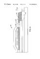
- a magnetic disk data storage systems 10 of the background artincludes a sealed enclosure 12 , a disk drive motor 14 , a magnetic disk 16 , supported for rotation by a drive spindle S 1 of motor 14 , an actuator 18 and an arm 20 attached to an actuator spindle S 2 of actuator 18 .
- a suspension 22is coupled at one end to the arm 20 , and at its other end to a read/write head or transducer 24 .
- the transducer 24(which will be described in greater detail with reference to FIG. 2A) typically includes an inductive write element with a sensor read element.
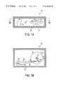
- FIG. 2Adepicts a magnetic read/write head 24 including a substrate 25 above which a read element 26 and a write element 28 are disposed. Edges of the read element 26 and write element 28 also define an air bearing surface ABS, in a plane 29 , which can be aligned to face the surface of the magnetic disk 16 (see FIG. 1 A and 1 B).
- the read element 26includes a first shield 30 , an intermediate layer 32 , which functions as a second shield, and a read sensor 34 that is located within a dielectric medium 35 between the first shield 30 and the second shield 32 .
- the most common type of read sensor 34 used in the read/write head 24is the magnetoresistive (AMR or GMR) sensor which is used to detect magnetic field signals from a magnetic medium through changing resistance in the read sensor.
- AMRmagnetoresistive
- the write element 28is typically an inductive write element which includes the intermediate layer 32 , which functions as a first pole, and a second pole 38 disposed above the first pole 32 .
- the first pole 32 and the second pole 38are attached to each other by a backgap portion 40 , with these three elements collectively forming a yoke 41 .
- the combination of a first pole tip portion 43 and a second pole tip portion 45 near the ABSare sometimes referred to as the yoke tip portion 46 .
- a write gap 36is formed between the first and second poles 32 , 38 in the yoke tip portion 46 .
- the write gap 36is filled with a non-magnetic electrically insulating material that forms a write gap material layer 37 . This non-magnetic material can be either integral with (as is shown here) or separate from a first insulation layer 47 that lies below the second yoke 38 and extends from the yoke tip portion 46 to the backgap portion 40 .
- a conductive coil 48formed of multiple winds 49 which each have a wind height Hw.
- the coil 48can be characterized by a dimension sometimes referred to as the wind pitch P, which is the distance from one coil wind front edge to the next coil wind front edge, as shown in FIG. 2 A.
- the wind pitch Pis defined by the sum of the wind thickness Tw and the separation between adjacent winds Sw.
- the conductive coil 48is positioned within a coil insulation layer 50 that lies above the first insulation layer 47 .
- the first insulation layer 47thereby electrically insulates the coil layer from the first pole 32
- the coil insulation layer 50electrically insulates the winds 49 from each other and from the second pole 38 .
- the configuration of the conductive coil 48can be better understood with reference to a plan view of the read/write head 24 shown in FIG. 2B taken along line 2 B— 2 B of FIG. 2 A. Because the conductive coil extends beyond the first and second poles, insulation may be needed beneath, as well as above, the conductive coil to electrically insulate the conductive coil from other structures. For example, as shown in FIG. 2C, a view taken along line 2 C— 2 C of FIG. 2A, a buildup insulation layer 52 can be formed adjacent the first pole, and under the conductive coil layer 48 . As is well known to those skilled in the art, these elements operate to magnetically write data on a magnetic medium such as a magnetic disk 16 (see FIGS. 1 A and 1 B).
- an inductive write headsuch as that shown in FIGS. 2A-2C operates by passing a writing current through the conductive coil layer 48 . Because of the magnetic properties of the yoke 41 , a magnetic flux is induced in the first and second poles 32 , 38 by write currents passed through the coil layer 48 .
- the write gap 36allows the magnetic flux to fringe out from the yoke 41 (thus forming a fringing gap field) and to cross a magnetic recording medium that is placed near the ABS.
- a critical parameter of a magnetic write elementis a trackwidth of the write element, which defines track density. For example, a narrower trackwidth can result in a higher magnetic recording density.
- the trackwidthis defined by geometries in the yoke tip portion 46 (see FIG. 2A) at the ABS. These geometries can be better understood with reference to FIG. 2 C.
- the first and second poles 32 , 38can have different widths W 1 , W 2 respectively in the yoke tip portion 46 (see FIG. 2 A).
- the trackwidth of the write element 28is defined by the width W 2 of the second pole 38 .
- the gap field of the write elementcan be affected by the throat height TH, which is measured from the ABS to the zero throat ZT, as shown in FIG. 2 A.
- accurate definition of the trackwidth and throat heightis critical during the fabrication of the write element.
- Another parameter of the write elementis the number of winds 49 in the coil layer 48 , which determines magnetic motive force (MMF) of a write element.
- MMFmagnetic motive force
- the number of windsis limited by the yoke length YL, shown in FIG. 2A, and the pitch P between adjacent winds 49 .
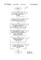
- the method 54includes providing a first pole with first and second edges in operation 56 .
- This operationcan include, for example, forming a plating dam, plating, and then removing the dam.
- a write gap material layeris formed over the first pole.
- the write gap material layeris formed over an upper surface and the first and second edges of the first pole.
- a viais formed through the write gap material layer to the first pole in the backgap portion 40 (see FIG. 2 A).
- the write gap material layerextends above the first pole in the area between the yoke tip portion and the backgap portion, although in other cases the write gap material layer may not be above this area.
- a buildup insulation layeris also formed in operation 60 , adjacent the first and second edges, with the write gap material layer between the first pole and the buildup insulation layer.
- the buildup insulation layeris typically formed by depositing (e.g., spinning) and patterning photoresistive material and then hard baking the remaining photoresistive material. Such processes often result in the height of the buildup insulation layer being non-uniform and different than the height of the write gap material layer, as is illustrated in FIGS. 2A and 2C.
- the method 54also includes forming a first coil layer above the write gap material layer and the buildup insulation layer in operation 62 .
- Thiscan include first depositing a seed layer above the first pole.
- photoresistive materialcan then be deposited and patterned. With the patterned photoresistive material in place, conductive material can be plated. With removal of the photoresistive material, the remaining conductive material thereby forms the coil.
- the patterning of the photoresistive material for the first coil layercan be complicated. In particular, it can be difficult to pattern the various heights to have consistent geometries. More specifically, winds of the resulting first coil layer can be wider at lower levels than at higher levels, such as between the first and second poles. Thus, for a given pitch, such greater width at the lower levels can result in smaller distances between winds. This can, in turn, result in electrical shorting between winds which can be detrimental to the write element performance. To avoid such electrical shorting, the minimum wind pitch can be set to a desired value that will result in adequate yield of non-shorting conductive coil layers.
- typical wind pitches between the first and second polesmay be limited to no less than about 3 microns. For a given number of winds and wind thickness, this in turn limits the minimum yoke length, and thereby limits the data transfer rate and data density as described above. For example, a pitch of about 3 microns may be adequate for recording densities on the order of about 2 Gb/sq.in., however, these typical pitches can be inadequate for larger recording densities, such as about 10 Gb/sq.in.
- the method 54further includes forming a coil insulation layer above the first coil layer that is formed in operation 62 .
- a second poleis formed above the coil insulation layer of operation 64 .
- Still another parameter of the write elementis the stack height SH, the distance between the top surface of the first pole 32 and the top of the second pole 38 , as shown in FIG. 2 A.
- this heightis affected by the thickness of the first insulation layer 47 , the thickness of the coil layer 48 and any other coil layers that might be included, and the height Hi of the coil insulation layer 50 and any other coil insulation layers that might be included.
- the stack height SHcan be an indicator of the apex angle ⁇ , which partially characterizes the topology over which the second pole must be formed near the yoke tip portion.
- the reliability of the write elementdecreases as the apex angle a increases.
- the definition of the second pole width W, shown in FIG. 2C, including photoresist deposition and etching,can be decreasingly reliable and precise with increasing topography.
- this aspect of fabricationbecomes increasingly problematic.
- yoke length YLmust be shortened in order to minimize flux rise time. This means that the pitch P of the coil 48 must be minimized, requiring a reduction in wind thickness Tw accordingly. The reduction in wind thickness leads to a corresponding increase in electrical resistance in the winds 49 .
- the number of winds 49 in a coil 48must be reduced.
- the current generated through the coilmust be increased in order to maintain a sufficient magnetic motive force.
- This increase in current through the coil 48 along with the increased resistance of the winds 49causes a dramatic increase in heat generation.
- the increased heat generated by a coil 48 of a high performance write element 28degrades the performance of the read element 26 .
- One reason for this decrease in performanceis that the heat will cause thermal stresses on the read/write head 24 as the various materials expand at different rates. These thermal stresses will in turn cause magnetic domain motion in shield 32 which generates magnetic flux into read sensor 34 . Due to magneto-resistive properties of the sensor, this undesired magnetic flux will be interpreted as a magnetic field.
- Another reason for this degradation of performanceis that heat conducted to the read sensor 34 will cause “Johnson Thermal Noise”. “Johnson Thermal Noise” is proportional to ( ⁇ )(K B T)(R) where ⁇ is the frequency of the signal being read, K B T is the temperature of the sensor in degrees Kelvin and R is the resistance of the sensor.
- the present inventionprovides a magnetic write head, and a method for manufacturing same, having a structure for dissipating heat.
- the write headincludes first and second magnetic poles joined at one end to form a yoke.
- a coil having a portion of its winds extending through the yokeimparts a magnetic flux through the yoke when an electrical current is caused to flow through the coil.
- the coilsits upon a layer of dielectric, thermally conductive material, which conducts and dissipates heat generated by the coil.
- the preferred embodiment of the present inventionincludes a read element and a write element combined to form a combination read/write head, all of which is built upon a ceramic substrate.
- the read portion of the headincludes a read sensor embedded within a first dielectric layer. This first dielectric layer is sandwiched between a first and a second shield.
- the second shield of the read elementserves as a portion of the first pole of the write element.
- the second shield/first polehas a flat upper surface, from which extends a write gap pedestal and a back gap pedestal.
- a second dielectric layeris formed over the first pole, and is planarized by a chemical mechanical polishing process. The polishing process exposes the flat upper surfaces of the pedestals and creates a smooth planar surface across the pedestals and the dielectric layer.
- the second dielectric layeris constructed of an electrically insulating, thermally conducting material, and extends laterally across the substrate beyond the first pole to provide an effective heat sink.
- the coilis formed, including a pair of contacts at the inner and outer ends of the coil.
- An insulation layeris deposited over the coil and formed so as to not cover the back gap or write gap pedestal.
- the insulation layeris formed with openings called “vias” at the location of the contacts of the coil.
- a thin layer of electrically insulating, non-magnetic materialis then deposited over the insulation layer and over the write gap pedestal. Again, the write gap material is formed so that it does not cover the back gap pedestal or the contacts of coil, although it does cover the write gap pedestal.
- the second poleis formed over the first pole.
- the back of the second polecontacts the back gap pedestal of the first pole, and the front of the second pole sits atop the write gap material above the write gap pedestal of the first pole.
- FIG. 1Ais a partial cross-sectional front elevation view of a magnetic data storage system
- FIG. 1Bis a top plan view taken along line 2 B— 2 B of FIG. 2A;
- FIG. 2Ais a cross-sectional view of a background art read/write head of the magnetic disk dive assembly of FIG. 1A and 1B;
- FIG. 2Bis a plan view taken along line 2 B— 2 B of FIG. 2A;
- FIG. 2Cis an ABS view taken along line 2 C— 2 C of FIG. 2A;
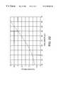
- FIG. 2Dis a representative graph of a relationship between yoke length and flux rise time
- FIG. 3is a process diagram of a method for forming a write element of the background art
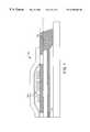
- FIG. 4is a cross sectional view of a read write head of the present invention taken along line 4 — 4 of FIG. 1B shown expanded and rotated 110 degrees clockwise.
- FIG. 5is an expanded view taken from region 5 of FIG. 4;
- FIG. 6is a plan view taken from line 6 — 6 of FIG. 4;
- FIG. 7is a view similar to view 5 of an alternate embodiment of the invention.
- FIG. 8is a view similar to view 5 of an alternate embodiment of the invention.
- FIG. 9is a process diagram of a method for forming a read/write head of the present invention.
- FIG. 4shows a cross sectional view of a read/write head 400 of the present invention.
- FIG. 5shows an expanded view taken from region 5 of FIG. 4 .
- the read/write head 500includes a read element 502 and a write element 504 disposed atop a ceramic substrate 506 .
- the read element 502 of the read/write head 500includes a first dielectric layer 508 sandwiched between first and second shields 510 and 512 .
- the read elementfurther includes a read sensor 514 embedded within the first dielectric layer 508 between the first and second shields 510 and 512 .
- the write element 504includes the second shield 512 which serves as a portion of a first pole 518 and has a planar upper surface 515 .
- a second pole 520joins with the first pole 518 to form a yoke 521 having a write gap portion 516 and a back gap portion 517 .
- a write gap pedestal 522located in the write gap portion 516 extends upward from the planar upper surface 515 .
- a back gap pedestalextends upward from the planar upper surface in the back gap portion 517 .
- the write gap pedestal 522 and the back gap pedestal 524each have flat upper surfaces 526 and 528 respectively which are coplanar across a plane 530 .
- a second dielectric layer 532covers the first pole 518 , surrounding the pedestals 522 and 524 . As shown more clearly in FIG. 6, the dielectric layer extends laterally beyond the first pole 518 .
- the second dielectric layeris planarized by a chemical mechanical polish (CMP) process which gives it a smooth, flat upper surface 534 which is coplanar with the plane 530 and flush with the upper surfaces 526 and 528 of the pedestals 522 and 524 .
- CMPchemical mechanical polish
- the second dielectric layer 532is constructed of a material which is both an electrical insulator and a thermal conductor.
- the thermal conductivity of the dielectric layershould be at least twice that of alumina (Al 2 O 3 ), preferably the thermal conductivity should be at or above 24 W/m o K at 40° Celsius and at or above 65 W/m o K at 20° Celsius. While several materials could provide the necessary electrical resistance and thermal conductance, in the preferred embodiment the dielectric layer is constructed of Al 3 N 4 , deposited by a reactive ion sputtering process. Alternatively, the second dielectric layer 532 could be constructed of Si 3 N 4 , or of Si 3 O 3 . The deposited planarized dielectric layer 532 has a thickness t which should be within the range of 1 ⁇ 2 to 1 ⁇ fraction (-1/2) ⁇ microns and is more preferably between 1 and 1 ⁇ fraction (-1/2) ⁇ microns.
- a coil 536is formed on top of the second dielectric layer such that a portion of the coil passes through the yoke 521 between the first and second poles 518 and 520 and between the write gap and back gap pedestals 522 and 524 respectively. While the coil 536 could be formed of any suitable conductive material, it is preferably formed of copper (Cu).
- the coil 536includes a plurality of winds 538 which define a pitch p, defined as the distance from an edge of a wind to the corresponding edge of an adjacent wind. Each wind has a wind thickness Tw. With reference to FIG. 6 the coil terminates at its inner and outer ends in first and second contacts 540 and 542 respectively.
- An insulation layer 541covers the coil 536 and electrically isolates it from the surrounding structure as well as isolating the winds 538 from one another.
- the insulation layer 541is preferably a photoresist which can be spun onto the coil 536 and the dielectric layer 532 and then cured.
- the insulation layer 541will be deposited over the entire structure formed thus far.
- the photoresistwill then be locally masked and lifted off in order to expose the write gap and back gap pedestals 522 and 524 and also to provide vias at the locations of the contacts 540 and 542 (FIG. 6 ).
- the insulation layer 540Once cured, the insulation layer 540 will define a gradually sloping edge 544 at the write gap portion. This gradually sloping edge will be beneficial in defining a low apex angle as will be described in more detail below.
- the insulation layer 541is covered with a thin layer of write gap material 546 which extends over and covers the upper surface 526 of the write gap pedestal 522 , thereby separating the first and second poles 518 and 520 in the write gap portion 516 of the yoke 521 .
- the write gap materialcan be formed of any suitable non-magnetic, electrically insulating material, such as alumina.
- the write gap material layer 546is formed so as not to cover the back gap pedestal 524 .
- the write gap material 546is formed to leave vias at the locations of the first and second contacts 540 and 542 .
- the second pole 520is formed over the write gap material layer 546 and also over the back gap pedestal 524 of the first pole, whereby the first and second poles, 518 and 520 , together form the yoke 521 .
- the second pole 520sits atop the write gap material 546 which in turn sits atop the write gap pedestal 522 .
- the space between the first and second poles 518 and 520 in the write gap portion 526defines a write gap 544 .
- an electrical currentwill be conducted through the coil 536 as supplied from the contacts 540 and 542 in order to generate a magnetic field as described in above in the background of the invention.
- Wthe amount of heat generated per second
- Ithe current flowing through the coil
- Ris the electrical resistance of the coil.
- the heatwill cause thermal stresses in the read write/head 500 as the various materials of which it is made expand at different rates. These thermal stresses will cause magnetic domain pattern reconstruction due to the magnetostriction of the magnetic materials used in the head.
- the magnetic domain movement in the shieldswill generate magnetic flux which passes through the read sensor. For a high sensitivity MR head, this undesired magnetic flux will be interpreted as a magnetic signal.
- the second problem created by the heat generationis that the heat itself when conducted to the read sensor, will degrade the performance of the read sensor 514 .
- Such degradation of read propertiesis called “Johnson Thermal Noise”, and is proportional to ( ⁇ )(K B T)(R) where ⁇ is the frequency of the signal being read, K B T is the temperature of the sensor in degrees Kelvin and R is the resistance of the sensor.
- the present inventionalleviates the effects of this heat generation.
- the high thermal conductivity of the second dielectric layer 532 on which the coil 536 sitsconducts heat away from the coil before that heat can be conducted through to the shield 512 and to the read sensor 514 .
- the thermally conductive dielectric layer 534extends laterally far beyond the yoke 521 and therefore provides a very large heat sink for dissipation of the heat from the coil.
- heat generated by the coil 536will conduct into the dielectric layer 532 and out of the yoke 521 into regions of the read/write head 500 remote from the read sensor 514 . This dissipation will also prevent thermal stresses on the read/write head 500 .
- the read sensor 514should preferably be a distance of 3-3 1 ⁇ 2 microns between the read sensor 514 and the write gap 516 of the write element 504 .
- a method 900 of manufacturing a read/write head of the present inventionwill now be described.
- the substrate 506is provided.
- the substrateis constructed of a ceramic material and is planarized to have a smooth flat upper surface.
- the first shield 510is formed on top of the ceramic substrate 506 .
- the first dielectric layer 508is formed and the read sensor 514 embedded therein.
- the second shield 512is formed over the first dielectric layer 508 and the first dielectric layer further built up to at least the top of the second shield 512 .
- the shield and built up dielectric layerare planarized by a CMP process which creates a smooth flat surface across the top of the shield 512 and the dielectric layer 508 .
- the write element 504can be formed using the shield 512 as a portion of the first pole 518 .
- the write gap and back gap pedestals 522 and 524are built up on top of the smooth, planar upper surface of the second shield 512 to form the first pole.
- the pedestals 522 and 524can be constructed of a magnetic material such as Ni 20 Fe 80 .
- the pedestals 522 and 524can be constructed of a high Magnetization material such as Ni 45 Fe 55 . Use of such high Magnetization materials can increase the magnetic performance of the write head, however such materials present manufacturing challenges due to their highly corrosive nature.
- the second dielectric layeris formed on top of the first pole 518 , covering the pedestals 522 and 524 . As shown more clearly with reference to FIG. 6, the second dielectric layer 532 extends beyond the first pole 518 to cover the first CMP dielectric layer 512 .
- This second dielectric layer 532should be constructed of an electrically insulating, thermally conductive material. While this second dielectric layer 532 could be constructed of any suitable thermally conductive, dielectric material, it is preferably constructed of Al 3 N 4 and deposited by a reactive sputtering process.
- the second dielectric layer 532could also be constructed of Si 3 N 4 and deposited by a chemical vapor deposition (CVD) process or constructed of Si 3 O 3 deposited by either sputtering or CVD. Then in a step 914 , the second dielectric layer 532 is planarized by a CMP process which exposes the upper surfaces 526 and 528 of pedestals 522 and 524 respectively. The CMP process is conducted sufficiently to generate smooth, flush, flat surfaces 526 , 524 and 534 along the plane 530 .
- CVDchemical vapor deposition
- the coil 536is formed on top of the second dielectric layer 532 .
- a layer of copper seedis deposited to provide a conductive surface on which to plate the copper coil.
- the copper coilis plated using photolithography to provide the desired shape.
- the remaining, exposed seed layercan be removed by an etching process.
- the insulation layer 541can be formed.
- the insulation layer 541is deposited as a photoresist which is spun onto the structure. The photoresist is masked, and lifted off to expose the pedestals 522 and 524 and to provide vias for the contacts 540 and 542 .
- the insulation layeris cured by thermal treatment in a furnace which solidifies the photoresist and causes it to have a gently sloped angle at its termination adjacent to the write gap pedestal 526 .
- the write gap material layer 546is deposited. While the write gap material can be of any suitable non-magnetic, electrically insulating material, the write gap material is preferably alumina (Al 2 O 3 ). After deposition, the write gap material layer can be etched to expose the back gap pedestal 524 and to provide a via at the locations of the contacts 540 and 542 . To complete the read/write head 500 , in a step 922 the second pole 520 is formed over the write gap material 546 and over the back gap pedestal 524 . The second pole 520 is preferably formed of Ni 20 Fe 80 and deposited by plating as understood by those skilled in the art.
- the second polecan be formed of a high Magnetization material such as Ni 45 Fe 55 and deposited by plating.
- the gradual slope 544 of the insulation layer 541 in the write gap portion 516will cause the pole to define a low apex angle 546 .
- This low apex angleimproves the magnetic flux flow at the write gap portion 516 of the yoke 521 , and allows the second pole to be formed with a more tightly controlled track-width.
- a single dielectric material matrix 702contains the read element 514 and serves as a substrate for the coil 536 .
- the entirety of the dielectric material 702consists of a thermally conductive, electrically insulating material.
- a thermally conductive, electrically insulating materialcould be Al 3 N 4 , Si 3 N 4 , or Si 3 O 3 .
- Such a designwould provide an increased heat sink for dissipation of heat from the coils. While certain head designs might require such an additional heat dissipation, this embodiment would also increase manufacturing costs due to the increased use of the thermally conductive materials.
- a first dielectric layer 802is constructed of an electrically insulating material such as alumina Al 2 O 3 as with the preferred embodiment. However, rather than extending to the top of the first shield, the first dielectric layer 802 extends only to the bottom of the second shield 510 . In this way, when the second dielectric is formed, it will have an increased thickness 806 in the region beyond the yoke 521 .
- the second insulation layer 804is constructed of a thermally conductive material as described in the preferred embodiment, however the increased thickness of the second dielectric layer 804 in the region outside of the yoke provides a larger heat sink, providing increased heat dissipation. While this embodiment entails increased manufacturing costs over the preferred embodiment it will not be as expensive as the embodiment illustrated in FIG. 7 which includes thermally conductive dielectric material 702 in both the read 502 and write 504 portions of the head.
- the write gap material layercan be deposited over the coil rather than over the insulation layer.
- the write gap materialcould be deposited over the second dielectric layer in which case the coil and insulation layer would be formed on top of the write gap material.
- the present inventionprovides a write head, and a method of manufacturing same, which solves the problems of heat generation inherent in high data rate read write heads.
- the present inventioneffectively conducts away and dissipates heat while incurring little additional manufacturing expense.
Landscapes
- Engineering & Computer Science (AREA)
- Manufacturing & Machinery (AREA)
- Physics & Mathematics (AREA)
- Electromagnetism (AREA)
- Magnetic Heads (AREA)
Abstract
Description
Claims (20)
Priority Applications (2)
| Application Number | Priority Date | Filing Date | Title |
|---|---|---|---|
| US09/379,892US6396660B1 (en) | 1999-08-23 | 1999-08-23 | Magnetic write element having a thermally dissipative structure |
| JP2000251384AJP2001110015A (en) | 1999-08-23 | 2000-08-22 | Thin film magnetic head, magnetic data storing system and method of producing thin film magnetic writing head |
Applications Claiming Priority (1)
| Application Number | Priority Date | Filing Date | Title |
|---|---|---|---|
| US09/379,892US6396660B1 (en) | 1999-08-23 | 1999-08-23 | Magnetic write element having a thermally dissipative structure |
Publications (1)
| Publication Number | Publication Date |
|---|---|
| US6396660B1true US6396660B1 (en) | 2002-05-28 |
Family
ID=23499139
Family Applications (1)
| Application Number | Title | Priority Date | Filing Date |
|---|---|---|---|
| US09/379,892Expired - LifetimeUS6396660B1 (en) | 1999-08-23 | 1999-08-23 | Magnetic write element having a thermally dissipative structure |
Country Status (2)
| Country | Link |
|---|---|
| US (1) | US6396660B1 (en) |
| JP (1) | JP2001110015A (en) |
Cited By (162)
| Publication number | Priority date | Publication date | Assignee | Title |
|---|---|---|---|---|
| US20010040764A1 (en)* | 2000-05-11 | 2001-11-15 | Tdk Corporation | Thin film magnetic head and method of manufacturing the same |
| US20020093772A1 (en)* | 2001-01-16 | 2002-07-18 | Tdk Corporation | Thin film magnetic head, magnetic head device and magnetic disk driving device |
| US20020145832A1 (en)* | 2001-04-04 | 2002-10-10 | Seagate Technology Llc | Perpendicular magnetic recording head with soft underlayer biasing |
| US20020154443A1 (en)* | 2001-01-09 | 2002-10-24 | Alps Electric Co., Ltd. | Soft magnetic film having high saturation magnetic flux density, thin film magnetic head using the same, and methods of producing the soft magnetic film and the thin film magnetic head |
| US20030048579A1 (en)* | 2001-09-12 | 2003-03-13 | Hitachi, Ltd. | Magnetic head, method of manufacturing the same and magnetic disc apparatus with the same |
| US20030067717A1 (en)* | 2001-10-05 | 2003-04-10 | Headway Technologies, Inc. | Thermal protrusion reduction in magnet heads by utilizing heat sink layers |
| GB2391104A (en)* | 2002-07-22 | 2004-01-28 | Alps Electric Co Ltd | Thin film magnetic head |
| US20040027719A1 (en)* | 2002-08-08 | 2004-02-12 | Savas Gider | Heat sink for a magnetic recording head |
| US20040027717A1 (en)* | 2002-08-07 | 2004-02-12 | Arshad Alfoqaha | Technique for reducing pole tip protrusion in a magnetic write head and GMR stripe temperature in an associated read head structure utilizing one or more internal diffuser regions |
| EP1398763A1 (en)* | 2002-08-08 | 2004-03-17 | Hitachi Global Storage Technologies Netherlands B.V. | Heat sink for a magnetic recording head |
| GB2393032A (en)* | 2002-09-13 | 2004-03-17 | Seagate Technology Llc | Magnetic head writer core structure having improved thermal dissipation properties |
| US20040080869A1 (en)* | 2002-10-29 | 2004-04-29 | Thompson Rea Christopher James | Magnetic head having a heat dissipating structure |
| US20040252396A1 (en)* | 2003-06-16 | 2004-12-16 | Seagate Technology Llc | Method and apparatus for mitigating thermal pole tip protrusion |
| US20050024764A1 (en)* | 2003-07-29 | 2005-02-03 | Hsiao Wen-Chien David | Magnetic head having a write coil structure with a reduced electrical resistance for reducing thermal protrusion |
| US20050024380A1 (en)* | 2003-07-28 | 2005-02-03 | Lin Lin | Method for reducing random access memory of IC in display devices |
| US20050047011A1 (en)* | 2003-08-25 | 2005-03-03 | Headway Technologies, Inc | Short yoke stitched writer with low DC coil resistance |
| US20050057841A1 (en)* | 2003-09-12 | 2005-03-17 | Seagate Technology Llc | Head with heating element and control regime therefor |
| US20050174685A1 (en)* | 2004-02-09 | 2005-08-11 | Headway Technologies, Inc. | Thin-film magnetic head |
| US20050225897A1 (en)* | 2004-04-13 | 2005-10-13 | Headway Technologies, Inc. | Heat extractor for magnetic reader-writer |
| US7009818B1 (en)* | 2002-12-30 | 2006-03-07 | Storage Technology Corporation | Thin film magnetic head having improved thermal characteristics, and method of manufacturing |
| US20060098337A1 (en)* | 2004-11-10 | 2006-05-11 | Hung-Chin Guthrie | Tungsten heat sink structures in a thin film magnetic head |
| US20060102956A1 (en)* | 2004-11-18 | 2006-05-18 | Seagate Technology Llc | Etch-stop layers for patterning block structures for reducing thermal protrusion |
| US7199974B1 (en)* | 2004-02-02 | 2007-04-03 | Western Digital (Fremont), Inc. | Read/write head with reduced pole tip protrusion |
| US7310204B1 (en) | 2003-12-19 | 2007-12-18 | Western Digital (Fremont), Llc | Inductive writer design for using a soft magnetic pedestal having a high magnetic saturation layer |
| US20100149687A1 (en)* | 2008-12-12 | 2010-06-17 | Headway Technologies, Inc. | Magnetic head that suppresses protrusion of medium facing surface caused by heat of coil |
| US20110044004A1 (en)* | 2009-08-18 | 2011-02-24 | Garosshen Thomas J | Heat transfer apparatus having a thermal interface material |
| US8514517B1 (en) | 2011-06-30 | 2013-08-20 | Western Digital (Fremont), Llc | Systems and methods for providing hybrid coils for magnetic write heads |
| US8547659B1 (en) | 2011-05-09 | 2013-10-01 | Western Digital (Fremont), Llc | System for providing a transducer having a main coil and an additional coil separated from the main pole by a write shield |
| US8817425B1 (en)* | 2013-03-15 | 2014-08-26 | Headway Technologies, Inc. | Dual-piece heat sink layer for robust reader in magnetic recording head |
| US8830628B1 (en) | 2009-02-23 | 2014-09-09 | Western Digital (Fremont), Llc | Method and system for providing a perpendicular magnetic recording head |
| US8879207B1 (en) | 2011-12-20 | 2014-11-04 | Western Digital (Fremont), Llc | Method for providing a side shield for a magnetic recording transducer using an air bridge |
| US8883017B1 (en) | 2013-03-12 | 2014-11-11 | Western Digital (Fremont), Llc | Method and system for providing a read transducer having seamless interfaces |
| US8917581B1 (en) | 2013-12-18 | 2014-12-23 | Western Digital Technologies, Inc. | Self-anneal process for a near field transducer and chimney in a hard disk drive assembly |
| US8923102B1 (en) | 2013-07-16 | 2014-12-30 | Western Digital (Fremont), Llc | Optical grating coupling for interferometric waveguides in heat assisted magnetic recording heads |
| US8947985B1 (en) | 2013-07-16 | 2015-02-03 | Western Digital (Fremont), Llc | Heat assisted magnetic recording transducers having a recessed pole |
| US8953422B1 (en) | 2014-06-10 | 2015-02-10 | Western Digital (Fremont), Llc | Near field transducer using dielectric waveguide core with fine ridge feature |
| US8958272B1 (en) | 2014-06-10 | 2015-02-17 | Western Digital (Fremont), Llc | Interfering near field transducer for energy assisted magnetic recording |
| US8970988B1 (en) | 2013-12-31 | 2015-03-03 | Western Digital (Fremont), Llc | Electric gaps and method for making electric gaps for multiple sensor arrays |
| US8971160B1 (en) | 2013-12-19 | 2015-03-03 | Western Digital (Fremont), Llc | Near field transducer with high refractive index pin for heat assisted magnetic recording |
| US8976635B1 (en) | 2014-06-10 | 2015-03-10 | Western Digital (Fremont), Llc | Near field transducer driven by a transverse electric waveguide for energy assisted magnetic recording |
| US8980109B1 (en) | 2012-12-11 | 2015-03-17 | Western Digital (Fremont), Llc | Method for providing a magnetic recording transducer using a combined main pole and side shield CMP for a wraparound shield scheme |
| US8982508B1 (en) | 2011-10-31 | 2015-03-17 | Western Digital (Fremont), Llc | Method for providing a side shield for a magnetic recording transducer |
| US8988812B1 (en) | 2013-11-27 | 2015-03-24 | Western Digital (Fremont), Llc | Multi-sensor array configuration for a two-dimensional magnetic recording (TDMR) operation |
| US8988825B1 (en) | 2014-02-28 | 2015-03-24 | Western Digital (Fremont, LLC | Method for fabricating a magnetic writer having half-side shields |
| US8984740B1 (en) | 2012-11-30 | 2015-03-24 | Western Digital (Fremont), Llc | Process for providing a magnetic recording transducer having a smooth magnetic seed layer |
| US8993217B1 (en) | 2013-04-04 | 2015-03-31 | Western Digital (Fremont), Llc | Double exposure technique for high resolution disk imaging |
| US8995087B1 (en) | 2006-11-29 | 2015-03-31 | Western Digital (Fremont), Llc | Perpendicular magnetic recording write head having a wrap around shield |
| US8997832B1 (en) | 2010-11-23 | 2015-04-07 | Western Digital (Fremont), Llc | Method of fabricating micrometer scale components |
| US9001628B1 (en) | 2013-12-16 | 2015-04-07 | Western Digital (Fremont), Llc | Assistant waveguides for evaluating main waveguide coupling efficiency and diode laser alignment tolerances for hard disk |
| US9001467B1 (en) | 2014-03-05 | 2015-04-07 | Western Digital (Fremont), Llc | Method for fabricating side shields in a magnetic writer |
| US9007879B1 (en) | 2014-06-10 | 2015-04-14 | Western Digital (Fremont), Llc | Interfering near field transducer having a wide metal bar feature for energy assisted magnetic recording |
| US9007719B1 (en) | 2013-10-23 | 2015-04-14 | Western Digital (Fremont), Llc | Systems and methods for using double mask techniques to achieve very small features |
| US9007725B1 (en) | 2014-10-07 | 2015-04-14 | Western Digital (Fremont), Llc | Sensor with positive coupling between dual ferromagnetic free layer laminates |
| US9013836B1 (en) | 2013-04-02 | 2015-04-21 | Western Digital (Fremont), Llc | Method and system for providing an antiferromagnetically coupled return pole |
| US9042052B1 (en) | 2014-06-23 | 2015-05-26 | Western Digital (Fremont), Llc | Magnetic writer having a partially shunted coil |
| US9042208B1 (en) | 2013-03-11 | 2015-05-26 | Western Digital Technologies, Inc. | Disk drive measuring fly height by applying a bias voltage to an electrically insulated write component of a head |
| US9042057B1 (en) | 2013-01-09 | 2015-05-26 | Western Digital (Fremont), Llc | Methods for providing magnetic storage elements with high magneto-resistance using Heusler alloys |
| US9042058B1 (en) | 2013-10-17 | 2015-05-26 | Western Digital Technologies, Inc. | Shield designed for middle shields in a multiple sensor array |
| US9042051B2 (en) | 2013-08-15 | 2015-05-26 | Western Digital (Fremont), Llc | Gradient write gap for perpendicular magnetic recording writer |
| US9053735B1 (en) | 2014-06-20 | 2015-06-09 | Western Digital (Fremont), Llc | Method for fabricating a magnetic writer using a full-film metal planarization |
| US9065043B1 (en) | 2012-06-29 | 2015-06-23 | Western Digital (Fremont), Llc | Tunnel magnetoresistance read head with narrow shield-to-shield spacing |
| US9064528B1 (en) | 2013-05-17 | 2015-06-23 | Western Digital Technologies, Inc. | Interferometric waveguide usable in shingled heat assisted magnetic recording in the absence of a near-field transducer |
| US9064527B1 (en) | 2013-04-12 | 2015-06-23 | Western Digital (Fremont), Llc | High order tapered waveguide for use in a heat assisted magnetic recording head |
| US9064507B1 (en) | 2009-07-31 | 2015-06-23 | Western Digital (Fremont), Llc | Magnetic etch-stop layer for magnetoresistive read heads |
| US9070381B1 (en) | 2013-04-12 | 2015-06-30 | Western Digital (Fremont), Llc | Magnetic recording read transducer having a laminated free layer |
| US9082423B1 (en) | 2013-12-18 | 2015-07-14 | Western Digital (Fremont), Llc | Magnetic recording write transducer having an improved trailing surface profile |
| US9087527B1 (en) | 2014-10-28 | 2015-07-21 | Western Digital (Fremont), Llc | Apparatus and method for middle shield connection in magnetic recording transducers |
| US9087534B1 (en) | 2011-12-20 | 2015-07-21 | Western Digital (Fremont), Llc | Method and system for providing a read transducer having soft and hard magnetic bias structures |
| US9093639B2 (en) | 2012-02-21 | 2015-07-28 | Western Digital (Fremont), Llc | Methods for manufacturing a magnetoresistive structure utilizing heating and cooling |
| US9104107B1 (en) | 2013-04-03 | 2015-08-11 | Western Digital (Fremont), Llc | DUV photoresist process |
| US9111550B1 (en) | 2014-12-04 | 2015-08-18 | Western Digital (Fremont), Llc | Write transducer having a magnetic buffer layer spaced between a side shield and a write pole by non-magnetic layers |
| US9111558B1 (en) | 2014-03-14 | 2015-08-18 | Western Digital (Fremont), Llc | System and method of diffractive focusing of light in a waveguide |
| US9111564B1 (en) | 2013-04-02 | 2015-08-18 | Western Digital (Fremont), Llc | Magnetic recording writer having a main pole with multiple flare angles |
| US9123362B1 (en) | 2011-03-22 | 2015-09-01 | Western Digital (Fremont), Llc | Methods for assembling an electrically assisted magnetic recording (EAMR) head |
| US9123358B1 (en) | 2012-06-11 | 2015-09-01 | Western Digital (Fremont), Llc | Conformal high moment side shield seed layer for perpendicular magnetic recording writer |
| US9123374B1 (en) | 2015-02-12 | 2015-09-01 | Western Digital (Fremont), Llc | Heat assisted magnetic recording writer having an integrated polarization rotation plate |
| US9123359B1 (en) | 2010-12-22 | 2015-09-01 | Western Digital (Fremont), Llc | Magnetic recording transducer with sputtered antiferromagnetic coupling trilayer between plated ferromagnetic shields and method of fabrication |
| US9135930B1 (en) | 2014-03-06 | 2015-09-15 | Western Digital (Fremont), Llc | Method for fabricating a magnetic write pole using vacuum deposition |
| US9135937B1 (en) | 2014-05-09 | 2015-09-15 | Western Digital (Fremont), Llc | Current modulation on laser diode for energy assisted magnetic recording transducer |
| US9142233B1 (en) | 2014-02-28 | 2015-09-22 | Western Digital (Fremont), Llc | Heat assisted magnetic recording writer having a recessed pole |
| US9147408B1 (en) | 2013-12-19 | 2015-09-29 | Western Digital (Fremont), Llc | Heated AFM layer deposition and cooling process for TMR magnetic recording sensor with high pinning field |
| US9147404B1 (en) | 2015-03-31 | 2015-09-29 | Western Digital (Fremont), Llc | Method and system for providing a read transducer having a dual free layer |
| US9153255B1 (en) | 2014-03-05 | 2015-10-06 | Western Digital (Fremont), Llc | Method for fabricating a magnetic writer having an asymmetric gap and shields |
| US9183854B2 (en) | 2014-02-24 | 2015-11-10 | Western Digital (Fremont), Llc | Method to make interferometric taper waveguide for HAMR light delivery |
| US9190085B1 (en) | 2014-03-12 | 2015-11-17 | Western Digital (Fremont), Llc | Waveguide with reflective grating for localized energy intensity |
| US9190079B1 (en) | 2014-09-22 | 2015-11-17 | Western Digital (Fremont), Llc | Magnetic write pole having engineered radius of curvature and chisel angle profiles |
| US9194692B1 (en) | 2013-12-06 | 2015-11-24 | Western Digital (Fremont), Llc | Systems and methods for using white light interferometry to measure undercut of a bi-layer structure |
| US9202493B1 (en) | 2014-02-28 | 2015-12-01 | Western Digital (Fremont), Llc | Method of making an ultra-sharp tip mode converter for a HAMR head |
| US9202480B2 (en) | 2009-10-14 | 2015-12-01 | Western Digital (Fremont), LLC. | Double patterning hard mask for damascene perpendicular magnetic recording (PMR) writer |
| US9214165B1 (en) | 2014-12-18 | 2015-12-15 | Western Digital (Fremont), Llc | Magnetic writer having a gradient in saturation magnetization of the shields |
| US9213322B1 (en) | 2012-08-16 | 2015-12-15 | Western Digital (Fremont), Llc | Methods for providing run to run process control using a dynamic tuner |
| US9214169B1 (en) | 2014-06-20 | 2015-12-15 | Western Digital (Fremont), Llc | Magnetic recording read transducer having a laminated free layer |
| US9214172B2 (en) | 2013-10-23 | 2015-12-15 | Western Digital (Fremont), Llc | Method of manufacturing a magnetic read head |
| US9230565B1 (en) | 2014-06-24 | 2016-01-05 | Western Digital (Fremont), Llc | Magnetic shield for magnetic recording head |
| US9236560B1 (en) | 2014-12-08 | 2016-01-12 | Western Digital (Fremont), Llc | Spin transfer torque tunneling magnetoresistive device having a laminated free layer with perpendicular magnetic anisotropy |
| US9245562B1 (en) | 2015-03-30 | 2016-01-26 | Western Digital (Fremont), Llc | Magnetic recording writer with a composite main pole |
| US9245545B1 (en) | 2013-04-12 | 2016-01-26 | Wester Digital (Fremont), Llc | Short yoke length coils for magnetic heads in disk drives |
| US9245543B1 (en) | 2010-06-25 | 2016-01-26 | Western Digital (Fremont), Llc | Method for providing an energy assisted magnetic recording head having a laser integrally mounted to the slider |
| US9251813B1 (en) | 2009-04-19 | 2016-02-02 | Western Digital (Fremont), Llc | Method of making a magnetic recording head |
| US9263071B1 (en) | 2015-03-31 | 2016-02-16 | Western Digital (Fremont), Llc | Flat NFT for heat assisted magnetic recording |
| US9263067B1 (en) | 2013-05-29 | 2016-02-16 | Western Digital (Fremont), Llc | Process for making PMR writer with constant side wall angle |
| US9269382B1 (en) | 2012-06-29 | 2016-02-23 | Western Digital (Fremont), Llc | Method and system for providing a read transducer having improved pinning of the pinned layer at higher recording densities |
| US9275657B1 (en) | 2013-08-14 | 2016-03-01 | Western Digital (Fremont), Llc | Process for making PMR writer with non-conformal side gaps |
| US9280990B1 (en) | 2013-12-11 | 2016-03-08 | Western Digital (Fremont), Llc | Method for fabricating a magnetic writer using multiple etches |
| US9286919B1 (en) | 2014-12-17 | 2016-03-15 | Western Digital (Fremont), Llc | Magnetic writer having a dual side gap |
| US9287494B1 (en) | 2013-06-28 | 2016-03-15 | Western Digital (Fremont), Llc | Magnetic tunnel junction (MTJ) with a magnesium oxide tunnel barrier |
| US9305583B1 (en) | 2014-02-18 | 2016-04-05 | Western Digital (Fremont), Llc | Method for fabricating a magnetic writer using multiple etches of damascene materials |
| US9312064B1 (en) | 2015-03-02 | 2016-04-12 | Western Digital (Fremont), Llc | Method to fabricate a magnetic head including ion milling of read gap using dual layer hard mask |
| US9318130B1 (en) | 2013-07-02 | 2016-04-19 | Western Digital (Fremont), Llc | Method to fabricate tunneling magnetic recording heads with extended pinned layer |
| US9336814B1 (en) | 2013-03-12 | 2016-05-10 | Western Digital (Fremont), Llc | Inverse tapered waveguide for use in a heat assisted magnetic recording head |
| US9343086B1 (en) | 2013-09-11 | 2016-05-17 | Western Digital (Fremont), Llc | Magnetic recording write transducer having an improved sidewall angle profile |
| US9343087B1 (en) | 2014-12-21 | 2016-05-17 | Western Digital (Fremont), Llc | Method for fabricating a magnetic writer having half shields |
| US9343098B1 (en) | 2013-08-23 | 2016-05-17 | Western Digital (Fremont), Llc | Method for providing a heat assisted magnetic recording transducer having protective pads |
| US9349394B1 (en) | 2013-10-18 | 2016-05-24 | Western Digital (Fremont), Llc | Method for fabricating a magnetic writer having a gradient side gap |
| US9349392B1 (en) | 2012-05-24 | 2016-05-24 | Western Digital (Fremont), Llc | Methods for improving adhesion on dielectric substrates |
| US9361913B1 (en) | 2013-06-03 | 2016-06-07 | Western Digital (Fremont), Llc | Recording read heads with a multi-layer AFM layer methods and apparatuses |
| US9361914B1 (en) | 2014-06-18 | 2016-06-07 | Western Digital (Fremont), Llc | Magnetic sensor with thin capping layer |
| US9368134B1 (en) | 2010-12-16 | 2016-06-14 | Western Digital (Fremont), Llc | Method and system for providing an antiferromagnetically coupled writer |
| US9384763B1 (en) | 2015-03-26 | 2016-07-05 | Western Digital (Fremont), Llc | Dual free layer magnetic reader having a rear bias structure including a soft bias layer |
| US9384765B1 (en) | 2015-09-24 | 2016-07-05 | Western Digital (Fremont), Llc | Method and system for providing a HAMR writer having improved optical efficiency |
| US9396742B1 (en) | 2012-11-30 | 2016-07-19 | Western Digital (Fremont), Llc | Magnetoresistive sensor for a magnetic storage system read head, and fabrication method thereof |
| US9396743B1 (en) | 2014-02-28 | 2016-07-19 | Western Digital (Fremont), Llc | Systems and methods for controlling soft bias thickness for tunnel magnetoresistance readers |
| US9406331B1 (en) | 2013-06-17 | 2016-08-02 | Western Digital (Fremont), Llc | Method for making ultra-narrow read sensor and read transducer device resulting therefrom |
| US9424866B1 (en) | 2015-09-24 | 2016-08-23 | Western Digital (Fremont), Llc | Heat assisted magnetic recording write apparatus having a dielectric gap |
| US9431038B1 (en) | 2015-06-29 | 2016-08-30 | Western Digital (Fremont), Llc | Method for fabricating a magnetic write pole having an improved sidewall angle profile |
| US9431047B1 (en) | 2013-05-01 | 2016-08-30 | Western Digital (Fremont), Llc | Method for providing an improved AFM reader shield |
| US9431031B1 (en) | 2015-03-24 | 2016-08-30 | Western Digital (Fremont), Llc | System and method for magnetic transducers having multiple sensors and AFC shields |
| US9431039B1 (en) | 2013-05-21 | 2016-08-30 | Western Digital (Fremont), Llc | Multiple sensor array usable in two-dimensional magnetic recording |
| US9431032B1 (en) | 2013-08-14 | 2016-08-30 | Western Digital (Fremont), Llc | Electrical connection arrangement for a multiple sensor array usable in two-dimensional magnetic recording |
| US9437251B1 (en) | 2014-12-22 | 2016-09-06 | Western Digital (Fremont), Llc | Apparatus and method having TDMR reader to reader shunts |
| US9441938B1 (en) | 2013-10-08 | 2016-09-13 | Western Digital (Fremont), Llc | Test structures for measuring near field transducer disc length |
| US9443541B1 (en) | 2015-03-24 | 2016-09-13 | Western Digital (Fremont), Llc | Magnetic writer having a gradient in saturation magnetization of the shields and return pole |
| US9449625B1 (en) | 2014-12-24 | 2016-09-20 | Western Digital (Fremont), Llc | Heat assisted magnetic recording head having a plurality of diffusion barrier layers |
| US9449621B1 (en) | 2015-03-26 | 2016-09-20 | Western Digital (Fremont), Llc | Dual free layer magnetic reader having a rear bias structure having a high aspect ratio |
| US9472216B1 (en) | 2015-09-23 | 2016-10-18 | Western Digital (Fremont), Llc | Differential dual free layer magnetic reader |
| US9484051B1 (en) | 2015-11-09 | 2016-11-01 | The Provost, Fellows, Foundation Scholars and the other members of Board, of the College of the Holy and Undivided Trinity of Queen Elizabeth near Dublin | Method and system for reducing undesirable reflections in a HAMR write apparatus |
| US9508372B1 (en) | 2015-06-03 | 2016-11-29 | Western Digital (Fremont), Llc | Shingle magnetic writer having a low sidewall angle pole |
| US9508365B1 (en) | 2015-06-24 | 2016-11-29 | Western Digital (Fremont), LLC. | Magnetic reader having a crystal decoupling structure |
| US9508363B1 (en) | 2014-06-17 | 2016-11-29 | Western Digital (Fremont), Llc | Method for fabricating a magnetic write pole having a leading edge bevel |
| US9530443B1 (en) | 2015-06-25 | 2016-12-27 | Western Digital (Fremont), Llc | Method for fabricating a magnetic recording device having a high aspect ratio structure |
| US9564150B1 (en) | 2015-11-24 | 2017-02-07 | Western Digital (Fremont), Llc | Magnetic read apparatus having an improved read sensor isolation circuit |
| US9595273B1 (en) | 2015-09-30 | 2017-03-14 | Western Digital (Fremont), Llc | Shingle magnetic writer having nonconformal shields |
| US9646639B2 (en) | 2015-06-26 | 2017-05-09 | Western Digital (Fremont), Llc | Heat assisted magnetic recording writer having integrated polarization rotation waveguides |
| US9666214B1 (en) | 2015-09-23 | 2017-05-30 | Western Digital (Fremont), Llc | Free layer magnetic reader that may have a reduced shield-to-shield spacing |
| US9721595B1 (en) | 2014-12-04 | 2017-08-01 | Western Digital (Fremont), Llc | Method for providing a storage device |
| US9741366B1 (en) | 2014-12-18 | 2017-08-22 | Western Digital (Fremont), Llc | Method for fabricating a magnetic writer having a gradient in saturation magnetization of the shields |
| US9740805B1 (en) | 2015-12-01 | 2017-08-22 | Western Digital (Fremont), Llc | Method and system for detecting hotspots for photolithographically-defined devices |
| US9754611B1 (en) | 2015-11-30 | 2017-09-05 | Western Digital (Fremont), Llc | Magnetic recording write apparatus having a stepped conformal trailing shield |
| US9767831B1 (en) | 2015-12-01 | 2017-09-19 | Western Digital (Fremont), Llc | Magnetic writer having convex trailing surface pole and conformal write gap |
| US9786301B1 (en) | 2014-12-02 | 2017-10-10 | Western Digital (Fremont), Llc | Apparatuses and methods for providing thin shields in a multiple sensor array |
| US9799351B1 (en) | 2015-11-30 | 2017-10-24 | Western Digital (Fremont), Llc | Short yoke length writer having assist coils |
| US9812155B1 (en) | 2015-11-23 | 2017-11-07 | Western Digital (Fremont), Llc | Method and system for fabricating high junction angle read sensors |
| US9842615B1 (en) | 2015-06-26 | 2017-12-12 | Western Digital (Fremont), Llc | Magnetic reader having a nonmagnetic insertion layer for the pinning layer |
| US9858951B1 (en) | 2015-12-01 | 2018-01-02 | Western Digital (Fremont), Llc | Method for providing a multilayer AFM layer in a read sensor |
| US9881638B1 (en) | 2014-12-17 | 2018-01-30 | Western Digital (Fremont), Llc | Method for providing a near-field transducer (NFT) for a heat assisted magnetic recording (HAMR) device |
| US9899042B1 (en)* | 2016-02-08 | 2018-02-20 | Seagate Technology Llc | Data writer with laminated front shield |
| US9934811B1 (en) | 2014-03-07 | 2018-04-03 | Western Digital (Fremont), Llc | Methods for controlling stray fields of magnetic features using magneto-elastic anisotropy |
| US9953670B1 (en) | 2015-11-10 | 2018-04-24 | Western Digital (Fremont), Llc | Method and system for providing a HAMR writer including a multi-mode interference device |
| US10037770B1 (en) | 2015-11-12 | 2018-07-31 | Western Digital (Fremont), Llc | Method for providing a magnetic recording write apparatus having a seamless pole |
| US10074387B1 (en) | 2014-12-21 | 2018-09-11 | Western Digital (Fremont), Llc | Method and system for providing a read transducer having symmetric antiferromagnetically coupled shields |
| US10636439B2 (en) | 2017-12-19 | 2020-04-28 | Western Digital Technologies, Inc. | MAMR write head with thermal dissipation conductive guide |
| US11217273B1 (en) | 2020-12-09 | 2022-01-04 | Seagate Technology Llc | Heat sinking layer between a substrate and encasing layers of a recording head |
Families Citing this family (1)
| Publication number | Priority date | Publication date | Assignee | Title |
|---|---|---|---|---|
| US8018675B2 (en) | 2008-03-06 | 2011-09-13 | Tdk Corporation | Thin film magnetic head |
Citations (27)
| Publication number | Priority date | Publication date | Assignee | Title |
|---|---|---|---|---|
| US4052749A (en) | 1976-05-19 | 1977-10-04 | Matsushita Electric Industrial Co., Ltd. | Thin film magnetic head |
| US4127884A (en) | 1976-03-30 | 1978-11-28 | Matsushita Electric Industrial Co., Ltd. | Magnetic head and method of making the same |
| US4429337A (en) | 1979-11-28 | 1984-01-31 | U.S. Philips Corporation | Magnetic head unit having thermally dissipating cover plate |
| US4639289A (en)* | 1984-02-03 | 1987-01-27 | Commissariat A L'energie Atomique | Process for producing a magnetic read - write head and head obtained by this process |
| US4924198A (en) | 1988-07-05 | 1990-05-08 | General Electric Company | Superconductive magnetic resonance magnet without cryogens |
| US5386275A (en) | 1992-09-30 | 1995-01-31 | Tokai Rubber Industries, Ltd. | Fluid-filled elastic mount having oscillating plate driven by electromagnetic means including magnet fixed to movable inner yoke member, and annular coil fixed to stationary outer yoke member |
| US5793578A (en) | 1996-11-15 | 1998-08-11 | International Business Machines Corporation | Thin film induction recording head having an inset first insulation layer that defines zero throat height and pole tip apex angle |
| US6028750A (en)* | 1997-04-25 | 2000-02-22 | Kyocera Corporation | Thin film magnetic head substrate with improved heat radiation |
| US6043959A (en)* | 1998-03-23 | 2000-03-28 | Read-Rite Corporation | Inductive write head formed with flat yoke and merged with magnetoresistive read transducer |
| US6104575A (en)* | 1997-09-05 | 2000-08-15 | Fujitsu Limited | Planar thin-film magnetic head and manufacturing method therefor |
| US6130805A (en)* | 1997-11-19 | 2000-10-10 | Tdk Corporation | Thin film magnetic head having upper pole chip formed over insulating layer |
| US6137662A (en)* | 1998-04-07 | 2000-10-24 | Read-Rite Corporation | Magnetoresistive sensor with pinned SAL |
| US6156375A (en)* | 1994-12-30 | 2000-12-05 | International Business Machines Corporation | Method of making read/write magnetoresistive (MR) head with sunken components |
| US6163436A (en)* | 1997-11-19 | 2000-12-19 | Tdk Corporation | Thin film magnet head with improved performance |
| US6166880A (en)* | 1991-08-13 | 2000-12-26 | Tdk Corporation | Thin film magnetic head which prevents errors due to electric discharge |
| US6169642B1 (en)* | 1997-10-15 | 2001-01-02 | Tdk Corporation | Thin-film magnetic head having a three-layer pole tip structure |
| US6168860B1 (en)* | 1993-07-23 | 2001-01-02 | Nonvolatile Electronics, Incorporated | Magnetic structure with stratified layers |
| US6171716B1 (en)* | 1998-05-26 | 2001-01-09 | Alps Electric Co., Ltd. | Soft magnetic film, and thin film magnetic head, planer magnetic element, and filter using the soft magnetic film |
| US6181514B1 (en)* | 1998-12-04 | 2001-01-30 | International Business Machines Corporation | Scaled write head with high recording density and high data rate |
| US6188544B1 (en)* | 1997-10-15 | 2001-02-13 | Tdk Corporation | Thin-film magnetic head with three-layer pole top structure |
| US6191495B1 (en)* | 1997-06-10 | 2001-02-20 | Lucent Technologies Inc. | Micromagnetic device having an anisotropic ferromagnetic core and method of manufacture therefor |
| US6191917B1 (en)* | 1998-09-10 | 2001-02-20 | Storage Technology Corporation | Thin film tape write head for dual frequency operation |
| US6191918B1 (en)* | 1998-10-23 | 2001-02-20 | International Business Machines Corporation | Embedded dual coil planar structure |
| US6191916B1 (en)* | 1998-03-30 | 2001-02-20 | Tdk Corporation | Thin film magnetic head and method of manufacturing the same |
| US6204999B1 (en)* | 1998-12-23 | 2001-03-20 | Read-Rite Corporation | Method and system for providing a write head having a conforming pole structure |
| US6204997B1 (en)* | 1998-05-19 | 2001-03-20 | Tdk Corporation | Thin film magnetic head with a plurality of engaged thin-film coils and method of manufacturing the same |
| US6207466B1 (en)* | 1998-09-22 | 2001-03-27 | Tdk Corporation | Method of manufacturing thin film magnetic head |
- 1999
- 1999-08-23USUS09/379,892patent/US6396660B1/ennot_activeExpired - Lifetime
- 2000
- 2000-08-22JPJP2000251384Apatent/JP2001110015A/enactivePending
Patent Citations (28)
| Publication number | Priority date | Publication date | Assignee | Title |
|---|---|---|---|---|
| US4127884A (en) | 1976-03-30 | 1978-11-28 | Matsushita Electric Industrial Co., Ltd. | Magnetic head and method of making the same |
| US4052749A (en) | 1976-05-19 | 1977-10-04 | Matsushita Electric Industrial Co., Ltd. | Thin film magnetic head |
| US4429337A (en) | 1979-11-28 | 1984-01-31 | U.S. Philips Corporation | Magnetic head unit having thermally dissipating cover plate |
| US4435900A (en) | 1979-11-28 | 1984-03-13 | U.S. Philips Corporation | Method of manufacturing a magnetic head unit |
| US4639289A (en)* | 1984-02-03 | 1987-01-27 | Commissariat A L'energie Atomique | Process for producing a magnetic read - write head and head obtained by this process |
| US4924198A (en) | 1988-07-05 | 1990-05-08 | General Electric Company | Superconductive magnetic resonance magnet without cryogens |
| US6166880A (en)* | 1991-08-13 | 2000-12-26 | Tdk Corporation | Thin film magnetic head which prevents errors due to electric discharge |
| US5386275A (en) | 1992-09-30 | 1995-01-31 | Tokai Rubber Industries, Ltd. | Fluid-filled elastic mount having oscillating plate driven by electromagnetic means including magnet fixed to movable inner yoke member, and annular coil fixed to stationary outer yoke member |
| US6168860B1 (en)* | 1993-07-23 | 2001-01-02 | Nonvolatile Electronics, Incorporated | Magnetic structure with stratified layers |
| US6156375A (en)* | 1994-12-30 | 2000-12-05 | International Business Machines Corporation | Method of making read/write magnetoresistive (MR) head with sunken components |
| US5793578A (en) | 1996-11-15 | 1998-08-11 | International Business Machines Corporation | Thin film induction recording head having an inset first insulation layer that defines zero throat height and pole tip apex angle |
| US6028750A (en)* | 1997-04-25 | 2000-02-22 | Kyocera Corporation | Thin film magnetic head substrate with improved heat radiation |
| US6191495B1 (en)* | 1997-06-10 | 2001-02-20 | Lucent Technologies Inc. | Micromagnetic device having an anisotropic ferromagnetic core and method of manufacture therefor |
| US6104575A (en)* | 1997-09-05 | 2000-08-15 | Fujitsu Limited | Planar thin-film magnetic head and manufacturing method therefor |
| US6169642B1 (en)* | 1997-10-15 | 2001-01-02 | Tdk Corporation | Thin-film magnetic head having a three-layer pole tip structure |
| US6188544B1 (en)* | 1997-10-15 | 2001-02-13 | Tdk Corporation | Thin-film magnetic head with three-layer pole top structure |
| US6163436A (en)* | 1997-11-19 | 2000-12-19 | Tdk Corporation | Thin film magnet head with improved performance |
| US6130805A (en)* | 1997-11-19 | 2000-10-10 | Tdk Corporation | Thin film magnetic head having upper pole chip formed over insulating layer |
| US6043959A (en)* | 1998-03-23 | 2000-03-28 | Read-Rite Corporation | Inductive write head formed with flat yoke and merged with magnetoresistive read transducer |
| US6191916B1 (en)* | 1998-03-30 | 2001-02-20 | Tdk Corporation | Thin film magnetic head and method of manufacturing the same |
| US6137662A (en)* | 1998-04-07 | 2000-10-24 | Read-Rite Corporation | Magnetoresistive sensor with pinned SAL |
| US6204997B1 (en)* | 1998-05-19 | 2001-03-20 | Tdk Corporation | Thin film magnetic head with a plurality of engaged thin-film coils and method of manufacturing the same |
| US6171716B1 (en)* | 1998-05-26 | 2001-01-09 | Alps Electric Co., Ltd. | Soft magnetic film, and thin film magnetic head, planer magnetic element, and filter using the soft magnetic film |
| US6191917B1 (en)* | 1998-09-10 | 2001-02-20 | Storage Technology Corporation | Thin film tape write head for dual frequency operation |
| US6207466B1 (en)* | 1998-09-22 | 2001-03-27 | Tdk Corporation | Method of manufacturing thin film magnetic head |
| US6191918B1 (en)* | 1998-10-23 | 2001-02-20 | International Business Machines Corporation | Embedded dual coil planar structure |
| US6181514B1 (en)* | 1998-12-04 | 2001-01-30 | International Business Machines Corporation | Scaled write head with high recording density and high data rate |
| US6204999B1 (en)* | 1998-12-23 | 2001-03-20 | Read-Rite Corporation | Method and system for providing a write head having a conforming pole structure |
Cited By (207)
| Publication number | Priority date | Publication date | Assignee | Title |
|---|---|---|---|---|
| US20010040764A1 (en)* | 2000-05-11 | 2001-11-15 | Tdk Corporation | Thin film magnetic head and method of manufacturing the same |
| US6731459B2 (en)* | 2000-05-11 | 2004-05-04 | Tdk Corporation | Thin film magnetic head |
| US20020154443A1 (en)* | 2001-01-09 | 2002-10-24 | Alps Electric Co., Ltd. | Soft magnetic film having high saturation magnetic flux density, thin film magnetic head using the same, and methods of producing the soft magnetic film and the thin film magnetic head |
| US6801392B2 (en)* | 2001-01-09 | 2004-10-05 | Alps Electric Co., Ltd. | Soft magnetic film having high saturation magnetic flux density, thin film magnetic head using the same, and methods of producing the soft magnetic film and the thin film magnetic head |
| US20020093772A1 (en)* | 2001-01-16 | 2002-07-18 | Tdk Corporation | Thin film magnetic head, magnetic head device and magnetic disk driving device |
| US6963474B2 (en)* | 2001-01-16 | 2005-11-08 | Tdk Corporation | Thin film magnetic head, magnetic head and magnetic disk driving device |
| US20020145832A1 (en)* | 2001-04-04 | 2002-10-10 | Seagate Technology Llc | Perpendicular magnetic recording head with soft underlayer biasing |
| US20030048579A1 (en)* | 2001-09-12 | 2003-03-13 | Hitachi, Ltd. | Magnetic head, method of manufacturing the same and magnetic disc apparatus with the same |
| US20050254173A1 (en)* | 2001-10-05 | 2005-11-17 | Headway Technologies, Inc. | Thermal protrusion reduction in magnet heads by utilizing heat sink layers |
| US20030067717A1 (en)* | 2001-10-05 | 2003-04-10 | Headway Technologies, Inc. | Thermal protrusion reduction in magnet heads by utilizing heat sink layers |
| US6914750B2 (en)* | 2001-10-05 | 2005-07-05 | Headway Technologies, Inc. | Thermal protrusion reduction in magnet heads by utilizing heat sink layers |
| US20040017638A1 (en)* | 2002-07-22 | 2004-01-29 | Alps Electric Co., Ltd. | Thin film magnetic head having improved heat radiating property |
| GB2391104A (en)* | 2002-07-22 | 2004-01-28 | Alps Electric Co Ltd | Thin film magnetic head |
| US6963470B2 (en)* | 2002-07-22 | 2005-11-08 | Alps Electic Co., Ltd. | Thin film magnetic head having improved heat radiating property |
| GB2391104B (en)* | 2002-07-22 | 2005-09-21 | Alps Electric Co Ltd | Thin film magnetic head |
| US20040027717A1 (en)* | 2002-08-07 | 2004-02-12 | Arshad Alfoqaha | Technique for reducing pole tip protrusion in a magnetic write head and GMR stripe temperature in an associated read head structure utilizing one or more internal diffuser regions |
| US6894871B2 (en)* | 2002-08-07 | 2005-05-17 | Western Digital (Fremont), Inc. | Technique for reducing pole tip protrusion in a magnetic write head and GMR stripe temperature in an associated read head structure utilizing one or more internal diffuser regions |
| EP1398763A1 (en)* | 2002-08-08 | 2004-03-17 | Hitachi Global Storage Technologies Netherlands B.V. | Heat sink for a magnetic recording head |
| CN100361200C (en)* | 2002-08-08 | 2008-01-09 | 日立环球储存科技荷兰有限公司 | Heat sinks for magnetic recording heads |
| US7170713B2 (en) | 2002-08-08 | 2007-01-30 | Hitachi Global Storage Technologies Netherlands B.V. | Heat sink for a magnetic recording head |
| US20040027719A1 (en)* | 2002-08-08 | 2004-02-12 | Savas Gider | Heat sink for a magnetic recording head |
| US6989963B2 (en) | 2002-09-13 | 2006-01-24 | Seagate Technology Llc | Writer core structures having improved thermal dissipation properties |
| GB2393032A (en)* | 2002-09-13 | 2004-03-17 | Seagate Technology Llc | Magnetic head writer core structure having improved thermal dissipation properties |
| US20040051996A1 (en)* | 2002-09-13 | 2004-03-18 | Seagate Technology Llc | Writer core structures having improved thermal dissipation properties |
| GB2393032B (en)* | 2002-09-13 | 2004-07-28 | Seagate Technology Llc | Writer core structures having improved thermal dissipation properties |
| US6950280B2 (en) | 2002-10-29 | 2005-09-27 | Seagate Technology Llc | Magnetic head having a heat dissipating structure |
| US20040080869A1 (en)* | 2002-10-29 | 2004-04-29 | Thompson Rea Christopher James | Magnetic head having a heat dissipating structure |
| US7009818B1 (en)* | 2002-12-30 | 2006-03-07 | Storage Technology Corporation | Thin film magnetic head having improved thermal characteristics, and method of manufacturing |
| US20040252396A1 (en)* | 2003-06-16 | 2004-12-16 | Seagate Technology Llc | Method and apparatus for mitigating thermal pole tip protrusion |
| US6867940B2 (en) | 2003-06-16 | 2005-03-15 | Seagate Technology Llc | Method and apparatus for mitigating thermal pole tip protrusion |
| US20050024380A1 (en)* | 2003-07-28 | 2005-02-03 | Lin Lin | Method for reducing random access memory of IC in display devices |
| US20050024764A1 (en)* | 2003-07-29 | 2005-02-03 | Hsiao Wen-Chien David | Magnetic head having a write coil structure with a reduced electrical resistance for reducing thermal protrusion |
| US7190552B2 (en) | 2003-07-29 | 2007-03-13 | Hitachi Global Storage Technologies Netherlands B.V. | Magnetic head having a damascene-fabricated write coil structure with coil layers extending between the poles for reduced electrical resistance |
| US7079353B2 (en)* | 2003-07-29 | 2006-07-18 | Hitachi Global Storage Technologies Netherlands B.V. | Magnetic head having a write coil structure with a reduced electrical resistance for reducing thermal protrusion |
| US20060152849A1 (en)* | 2003-07-29 | 2006-07-13 | Hsiao Wen-Chien D | Magnetic head having a write coil structure with a reduced electrical resistance for reducing thermal protrusion |
| US7047625B2 (en) | 2003-08-25 | 2006-05-23 | Headway Technologies, Inc. | Planarizing process |
| US20050047011A1 (en)* | 2003-08-25 | 2005-03-03 | Headway Technologies, Inc | Short yoke stitched writer with low DC coil resistance |
| US6975472B2 (en) | 2003-09-12 | 2005-12-13 | Seagate Technology Llc | Head with heating element and control regime therefor |
| US20050057841A1 (en)* | 2003-09-12 | 2005-03-17 | Seagate Technology Llc | Head with heating element and control regime therefor |
| US7375926B1 (en) | 2003-12-19 | 2008-05-20 | Western Digital (Fremont), Llc | Inductive writer design using a soft magnetic pedestal having a high magnetic saturation layer |
| US7310204B1 (en) | 2003-12-19 | 2007-12-18 | Western Digital (Fremont), Llc | Inductive writer design for using a soft magnetic pedestal having a high magnetic saturation layer |
| US7199974B1 (en)* | 2004-02-02 | 2007-04-03 | Western Digital (Fremont), Inc. | Read/write head with reduced pole tip protrusion |
| US20050174685A1 (en)* | 2004-02-09 | 2005-08-11 | Headway Technologies, Inc. | Thin-film magnetic head |
| US7173792B2 (en)* | 2004-02-09 | 2007-02-06 | Headway Technologies, Inc. | Thin-film magnetic head having a cooling layer formed coplanar with a lower pole and from the same material as the lower pole |
| US7748439B2 (en)* | 2004-04-13 | 2010-07-06 | Headway Technologies, Inc. | Heat extractor for magnetic reader-writer |
| US20050225897A1 (en)* | 2004-04-13 | 2005-10-13 | Headway Technologies, Inc. | Heat extractor for magnetic reader-writer |
| US20060098337A1 (en)* | 2004-11-10 | 2006-05-11 | Hung-Chin Guthrie | Tungsten heat sink structures in a thin film magnetic head |
| US20060102956A1 (en)* | 2004-11-18 | 2006-05-18 | Seagate Technology Llc | Etch-stop layers for patterning block structures for reducing thermal protrusion |
| US7411264B2 (en) | 2004-11-18 | 2008-08-12 | Seagate Technology Llc | Etch-stop layers for patterning block structures for reducing thermal protrusion |
| US8995087B1 (en) | 2006-11-29 | 2015-03-31 | Western Digital (Fremont), Llc | Perpendicular magnetic recording write head having a wrap around shield |
| US20100149687A1 (en)* | 2008-12-12 | 2010-06-17 | Headway Technologies, Inc. | Magnetic head that suppresses protrusion of medium facing surface caused by heat of coil |
| US8184398B2 (en)* | 2008-12-12 | 2012-05-22 | Headway Technologies, Inc. | Magnetic head that suppresses protrusion of medium facing surface caused by heat of coil |
| US8830628B1 (en) | 2009-02-23 | 2014-09-09 | Western Digital (Fremont), Llc | Method and system for providing a perpendicular magnetic recording head |
| US9251813B1 (en) | 2009-04-19 | 2016-02-02 | Western Digital (Fremont), Llc | Method of making a magnetic recording head |
| US9064507B1 (en) | 2009-07-31 | 2015-06-23 | Western Digital (Fremont), Llc | Magnetic etch-stop layer for magnetoresistive read heads |
| US20110044004A1 (en)* | 2009-08-18 | 2011-02-24 | Garosshen Thomas J | Heat transfer apparatus having a thermal interface material |
| US9202480B2 (en) | 2009-10-14 | 2015-12-01 | Western Digital (Fremont), LLC. | Double patterning hard mask for damascene perpendicular magnetic recording (PMR) writer |
| US9245543B1 (en) | 2010-06-25 | 2016-01-26 | Western Digital (Fremont), Llc | Method for providing an energy assisted magnetic recording head having a laser integrally mounted to the slider |
| US9672847B2 (en) | 2010-11-23 | 2017-06-06 | Western Digital (Fremont), Llc | Micrometer scale components |
| US8997832B1 (en) | 2010-11-23 | 2015-04-07 | Western Digital (Fremont), Llc | Method of fabricating micrometer scale components |
| US9159345B1 (en) | 2010-11-23 | 2015-10-13 | Western Digital (Fremont), Llc | Micrometer scale components |
| US9368134B1 (en) | 2010-12-16 | 2016-06-14 | Western Digital (Fremont), Llc | Method and system for providing an antiferromagnetically coupled writer |
| US9123359B1 (en) | 2010-12-22 | 2015-09-01 | Western Digital (Fremont), Llc | Magnetic recording transducer with sputtered antiferromagnetic coupling trilayer between plated ferromagnetic shields and method of fabrication |
| US9123362B1 (en) | 2011-03-22 | 2015-09-01 | Western Digital (Fremont), Llc | Methods for assembling an electrically assisted magnetic recording (EAMR) head |
| US8547659B1 (en) | 2011-05-09 | 2013-10-01 | Western Digital (Fremont), Llc | System for providing a transducer having a main coil and an additional coil separated from the main pole by a write shield |
| US9117464B1 (en) | 2011-06-30 | 2015-08-25 | Western Digital (Fremont), Llc | Methods for manufacturing hybrid coils for magnetic write heads used in storage systems |
| US8514517B1 (en) | 2011-06-30 | 2013-08-20 | Western Digital (Fremont), Llc | Systems and methods for providing hybrid coils for magnetic write heads |
| US8982508B1 (en) | 2011-10-31 | 2015-03-17 | Western Digital (Fremont), Llc | Method for providing a side shield for a magnetic recording transducer |
| US8879207B1 (en) | 2011-12-20 | 2014-11-04 | Western Digital (Fremont), Llc | Method for providing a side shield for a magnetic recording transducer using an air bridge |
| US9087534B1 (en) | 2011-12-20 | 2015-07-21 | Western Digital (Fremont), Llc | Method and system for providing a read transducer having soft and hard magnetic bias structures |
| US9093639B2 (en) | 2012-02-21 | 2015-07-28 | Western Digital (Fremont), Llc | Methods for manufacturing a magnetoresistive structure utilizing heating and cooling |
| US9349392B1 (en) | 2012-05-24 | 2016-05-24 | Western Digital (Fremont), Llc | Methods for improving adhesion on dielectric substrates |
| US9940950B2 (en) | 2012-05-24 | 2018-04-10 | Western Digital (Fremont), Llc | Methods for improving adhesion on dielectric substrates |
| US9123358B1 (en) | 2012-06-11 | 2015-09-01 | Western Digital (Fremont), Llc | Conformal high moment side shield seed layer for perpendicular magnetic recording writer |
| US9269382B1 (en) | 2012-06-29 | 2016-02-23 | Western Digital (Fremont), Llc | Method and system for providing a read transducer having improved pinning of the pinned layer at higher recording densities |
| US9412400B2 (en) | 2012-06-29 | 2016-08-09 | Western Digital (Fremont), Llc | Tunnel magnetoresistance read head with narrow shield-to-shield spacing |
| US9065043B1 (en) | 2012-06-29 | 2015-06-23 | Western Digital (Fremont), Llc | Tunnel magnetoresistance read head with narrow shield-to-shield spacing |
| US9213322B1 (en) | 2012-08-16 | 2015-12-15 | Western Digital (Fremont), Llc | Methods for providing run to run process control using a dynamic tuner |
| US9396742B1 (en) | 2012-11-30 | 2016-07-19 | Western Digital (Fremont), Llc | Magnetoresistive sensor for a magnetic storage system read head, and fabrication method thereof |
| US8984740B1 (en) | 2012-11-30 | 2015-03-24 | Western Digital (Fremont), Llc | Process for providing a magnetic recording transducer having a smooth magnetic seed layer |
| US8980109B1 (en) | 2012-12-11 | 2015-03-17 | Western Digital (Fremont), Llc | Method for providing a magnetic recording transducer using a combined main pole and side shield CMP for a wraparound shield scheme |
| US9042057B1 (en) | 2013-01-09 | 2015-05-26 | Western Digital (Fremont), Llc | Methods for providing magnetic storage elements with high magneto-resistance using Heusler alloys |
| US9042208B1 (en) | 2013-03-11 | 2015-05-26 | Western Digital Technologies, Inc. | Disk drive measuring fly height by applying a bias voltage to an electrically insulated write component of a head |
| US9336814B1 (en) | 2013-03-12 | 2016-05-10 | Western Digital (Fremont), Llc | Inverse tapered waveguide for use in a heat assisted magnetic recording head |
| US8883017B1 (en) | 2013-03-12 | 2014-11-11 | Western Digital (Fremont), Llc | Method and system for providing a read transducer having seamless interfaces |
| US8817425B1 (en)* | 2013-03-15 | 2014-08-26 | Headway Technologies, Inc. | Dual-piece heat sink layer for robust reader in magnetic recording head |
| US9111564B1 (en) | 2013-04-02 | 2015-08-18 | Western Digital (Fremont), Llc | Magnetic recording writer having a main pole with multiple flare angles |
| US9013836B1 (en) | 2013-04-02 | 2015-04-21 | Western Digital (Fremont), Llc | Method and system for providing an antiferromagnetically coupled return pole |
| US9104107B1 (en) | 2013-04-03 | 2015-08-11 | Western Digital (Fremont), Llc | DUV photoresist process |
| US8993217B1 (en) | 2013-04-04 | 2015-03-31 | Western Digital (Fremont), Llc | Double exposure technique for high resolution disk imaging |
| US9070381B1 (en) | 2013-04-12 | 2015-06-30 | Western Digital (Fremont), Llc | Magnetic recording read transducer having a laminated free layer |
| US9064527B1 (en) | 2013-04-12 | 2015-06-23 | Western Digital (Fremont), Llc | High order tapered waveguide for use in a heat assisted magnetic recording head |
| US9245545B1 (en) | 2013-04-12 | 2016-01-26 | Wester Digital (Fremont), Llc | Short yoke length coils for magnetic heads in disk drives |
| US9431047B1 (en) | 2013-05-01 | 2016-08-30 | Western Digital (Fremont), Llc | Method for providing an improved AFM reader shield |
| US9064528B1 (en) | 2013-05-17 | 2015-06-23 | Western Digital Technologies, Inc. | Interferometric waveguide usable in shingled heat assisted magnetic recording in the absence of a near-field transducer |
| US9431039B1 (en) | 2013-05-21 | 2016-08-30 | Western Digital (Fremont), Llc | Multiple sensor array usable in two-dimensional magnetic recording |
| US9263067B1 (en) | 2013-05-29 | 2016-02-16 | Western Digital (Fremont), Llc | Process for making PMR writer with constant side wall angle |
| US9361913B1 (en) | 2013-06-03 | 2016-06-07 | Western Digital (Fremont), Llc | Recording read heads with a multi-layer AFM layer methods and apparatuses |
| US9406331B1 (en) | 2013-06-17 | 2016-08-02 | Western Digital (Fremont), Llc | Method for making ultra-narrow read sensor and read transducer device resulting therefrom |
| US9287494B1 (en) | 2013-06-28 | 2016-03-15 | Western Digital (Fremont), Llc | Magnetic tunnel junction (MTJ) with a magnesium oxide tunnel barrier |
| US9318130B1 (en) | 2013-07-02 | 2016-04-19 | Western Digital (Fremont), Llc | Method to fabricate tunneling magnetic recording heads with extended pinned layer |
| US8923102B1 (en) | 2013-07-16 | 2014-12-30 | Western Digital (Fremont), Llc | Optical grating coupling for interferometric waveguides in heat assisted magnetic recording heads |
| US8947985B1 (en) | 2013-07-16 | 2015-02-03 | Western Digital (Fremont), Llc | Heat assisted magnetic recording transducers having a recessed pole |
| US9431032B1 (en) | 2013-08-14 | 2016-08-30 | Western Digital (Fremont), Llc | Electrical connection arrangement for a multiple sensor array usable in two-dimensional magnetic recording |
| US9275657B1 (en) | 2013-08-14 | 2016-03-01 | Western Digital (Fremont), Llc | Process for making PMR writer with non-conformal side gaps |
| US9042051B2 (en) | 2013-08-15 | 2015-05-26 | Western Digital (Fremont), Llc | Gradient write gap for perpendicular magnetic recording writer |
| US9343098B1 (en) | 2013-08-23 | 2016-05-17 | Western Digital (Fremont), Llc | Method for providing a heat assisted magnetic recording transducer having protective pads |
| US9343086B1 (en) | 2013-09-11 | 2016-05-17 | Western Digital (Fremont), Llc | Magnetic recording write transducer having an improved sidewall angle profile |
| US9441938B1 (en) | 2013-10-08 | 2016-09-13 | Western Digital (Fremont), Llc | Test structures for measuring near field transducer disc length |
| US9042058B1 (en) | 2013-10-17 | 2015-05-26 | Western Digital Technologies, Inc. | Shield designed for middle shields in a multiple sensor array |
| US9349394B1 (en) | 2013-10-18 | 2016-05-24 | Western Digital (Fremont), Llc | Method for fabricating a magnetic writer having a gradient side gap |
| US9830936B2 (en) | 2013-10-23 | 2017-11-28 | Western Digital (Fremont), Llc | Magnetic read head with antiferromagentic layer |
| US9007719B1 (en) | 2013-10-23 | 2015-04-14 | Western Digital (Fremont), Llc | Systems and methods for using double mask techniques to achieve very small features |
| US9214172B2 (en) | 2013-10-23 | 2015-12-15 | Western Digital (Fremont), Llc | Method of manufacturing a magnetic read head |
| US8988812B1 (en) | 2013-11-27 | 2015-03-24 | Western Digital (Fremont), Llc | Multi-sensor array configuration for a two-dimensional magnetic recording (TDMR) operation |
| US9194692B1 (en) | 2013-12-06 | 2015-11-24 | Western Digital (Fremont), Llc | Systems and methods for using white light interferometry to measure undercut of a bi-layer structure |
| US9280990B1 (en) | 2013-12-11 | 2016-03-08 | Western Digital (Fremont), Llc | Method for fabricating a magnetic writer using multiple etches |
| US9001628B1 (en) | 2013-12-16 | 2015-04-07 | Western Digital (Fremont), Llc | Assistant waveguides for evaluating main waveguide coupling efficiency and diode laser alignment tolerances for hard disk |
| US8917581B1 (en) | 2013-12-18 | 2014-12-23 | Western Digital Technologies, Inc. | Self-anneal process for a near field transducer and chimney in a hard disk drive assembly |
| US9082423B1 (en) | 2013-12-18 | 2015-07-14 | Western Digital (Fremont), Llc | Magnetic recording write transducer having an improved trailing surface profile |
| US9147408B1 (en) | 2013-12-19 | 2015-09-29 | Western Digital (Fremont), Llc | Heated AFM layer deposition and cooling process for TMR magnetic recording sensor with high pinning field |
| US8971160B1 (en) | 2013-12-19 | 2015-03-03 | Western Digital (Fremont), Llc | Near field transducer with high refractive index pin for heat assisted magnetic recording |
| US8970988B1 (en) | 2013-12-31 | 2015-03-03 | Western Digital (Fremont), Llc | Electric gaps and method for making electric gaps for multiple sensor arrays |
| US9305583B1 (en) | 2014-02-18 | 2016-04-05 | Western Digital (Fremont), Llc | Method for fabricating a magnetic writer using multiple etches of damascene materials |
| US9183854B2 (en) | 2014-02-24 | 2015-11-10 | Western Digital (Fremont), Llc | Method to make interferometric taper waveguide for HAMR light delivery |
| US9142233B1 (en) | 2014-02-28 | 2015-09-22 | Western Digital (Fremont), Llc | Heat assisted magnetic recording writer having a recessed pole |
| US9202493B1 (en) | 2014-02-28 | 2015-12-01 | Western Digital (Fremont), Llc | Method of making an ultra-sharp tip mode converter for a HAMR head |
| US9396743B1 (en) | 2014-02-28 | 2016-07-19 | Western Digital (Fremont), Llc | Systems and methods for controlling soft bias thickness for tunnel magnetoresistance readers |
| US8988825B1 (en) | 2014-02-28 | 2015-03-24 | Western Digital (Fremont, LLC | Method for fabricating a magnetic writer having half-side shields |
| US9001467B1 (en) | 2014-03-05 | 2015-04-07 | Western Digital (Fremont), Llc | Method for fabricating side shields in a magnetic writer |
| US9349393B2 (en) | 2014-03-05 | 2016-05-24 | Western Digital (Fremont), Llc | Magnetic writer having an asymmetric gap and shields |
| US9153255B1 (en) | 2014-03-05 | 2015-10-06 | Western Digital (Fremont), Llc | Method for fabricating a magnetic writer having an asymmetric gap and shields |
| US9135930B1 (en) | 2014-03-06 | 2015-09-15 | Western Digital (Fremont), Llc | Method for fabricating a magnetic write pole using vacuum deposition |
| US9934811B1 (en) | 2014-03-07 | 2018-04-03 | Western Digital (Fremont), Llc | Methods for controlling stray fields of magnetic features using magneto-elastic anisotropy |
| US9495984B2 (en) | 2014-03-12 | 2016-11-15 | Western Digital (Fremont), Llc | Waveguide with reflective grating for localized energy intensity |
| US9190085B1 (en) | 2014-03-12 | 2015-11-17 | Western Digital (Fremont), Llc | Waveguide with reflective grating for localized energy intensity |
| US9111558B1 (en) | 2014-03-14 | 2015-08-18 | Western Digital (Fremont), Llc | System and method of diffractive focusing of light in a waveguide |
| US9135937B1 (en) | 2014-05-09 | 2015-09-15 | Western Digital (Fremont), Llc | Current modulation on laser diode for energy assisted magnetic recording transducer |
| US8976635B1 (en) | 2014-06-10 | 2015-03-10 | Western Digital (Fremont), Llc | Near field transducer driven by a transverse electric waveguide for energy assisted magnetic recording |
| US8958272B1 (en) | 2014-06-10 | 2015-02-17 | Western Digital (Fremont), Llc | Interfering near field transducer for energy assisted magnetic recording |
| US9311952B2 (en) | 2014-06-10 | 2016-04-12 | Western Digital (Fremont), Llc | Interfering near field transducer for energy assisted magnetic recording |
| US9159346B1 (en) | 2014-06-10 | 2015-10-13 | Western Digital (Fremont), Llc | Near field transducer using dielectric waveguide core with fine ridge feature |
| US8953422B1 (en) | 2014-06-10 | 2015-02-10 | Western Digital (Fremont), Llc | Near field transducer using dielectric waveguide core with fine ridge feature |
| US9007879B1 (en) | 2014-06-10 | 2015-04-14 | Western Digital (Fremont), Llc | Interfering near field transducer having a wide metal bar feature for energy assisted magnetic recording |
| US9508363B1 (en) | 2014-06-17 | 2016-11-29 | Western Digital (Fremont), Llc | Method for fabricating a magnetic write pole having a leading edge bevel |
| US9361914B1 (en) | 2014-06-18 | 2016-06-07 | Western Digital (Fremont), Llc | Magnetic sensor with thin capping layer |
| US9053735B1 (en) | 2014-06-20 | 2015-06-09 | Western Digital (Fremont), Llc | Method for fabricating a magnetic writer using a full-film metal planarization |
| US9214169B1 (en) | 2014-06-20 | 2015-12-15 | Western Digital (Fremont), Llc | Magnetic recording read transducer having a laminated free layer |
| US9042052B1 (en) | 2014-06-23 | 2015-05-26 | Western Digital (Fremont), Llc | Magnetic writer having a partially shunted coil |
| US9230565B1 (en) | 2014-06-24 | 2016-01-05 | Western Digital (Fremont), Llc | Magnetic shield for magnetic recording head |
| US9190079B1 (en) | 2014-09-22 | 2015-11-17 | Western Digital (Fremont), Llc | Magnetic write pole having engineered radius of curvature and chisel angle profiles |
| US9007725B1 (en) | 2014-10-07 | 2015-04-14 | Western Digital (Fremont), Llc | Sensor with positive coupling between dual ferromagnetic free layer laminates |
| US9087527B1 (en) | 2014-10-28 | 2015-07-21 | Western Digital (Fremont), Llc | Apparatus and method for middle shield connection in magnetic recording transducers |
| US9786301B1 (en) | 2014-12-02 | 2017-10-10 | Western Digital (Fremont), Llc | Apparatuses and methods for providing thin shields in a multiple sensor array |
| US9111550B1 (en) | 2014-12-04 | 2015-08-18 | Western Digital (Fremont), Llc | Write transducer having a magnetic buffer layer spaced between a side shield and a write pole by non-magnetic layers |
| US9721595B1 (en) | 2014-12-04 | 2017-08-01 | Western Digital (Fremont), Llc | Method for providing a storage device |
| US9236560B1 (en) | 2014-12-08 | 2016-01-12 | Western Digital (Fremont), Llc | Spin transfer torque tunneling magnetoresistive device having a laminated free layer with perpendicular magnetic anisotropy |
| US9705072B2 (en) | 2014-12-08 | 2017-07-11 | Western Digital (Fremont), Llc | Spin transfer torque tunneling magnetoresistive device having a laminated free layer with perpendicular magnetic anisotropy |
| US10553241B2 (en) | 2014-12-17 | 2020-02-04 | Western Digital Technologies, Inc. | Near-field transducer (NFT) for a heat assisted magnetic recording (HAMR) device |
| US9286919B1 (en) | 2014-12-17 | 2016-03-15 | Western Digital (Fremont), Llc | Magnetic writer having a dual side gap |
| US9881638B1 (en) | 2014-12-17 | 2018-01-30 | Western Digital (Fremont), Llc | Method for providing a near-field transducer (NFT) for a heat assisted magnetic recording (HAMR) device |
| US9214165B1 (en) | 2014-12-18 | 2015-12-15 | Western Digital (Fremont), Llc | Magnetic writer having a gradient in saturation magnetization of the shields |
| US9741366B1 (en) | 2014-12-18 | 2017-08-22 | Western Digital (Fremont), Llc | Method for fabricating a magnetic writer having a gradient in saturation magnetization of the shields |
| US10074387B1 (en) | 2014-12-21 | 2018-09-11 | Western Digital (Fremont), Llc | Method and system for providing a read transducer having symmetric antiferromagnetically coupled shields |
| US9343087B1 (en) | 2014-12-21 | 2016-05-17 | Western Digital (Fremont), Llc | Method for fabricating a magnetic writer having half shields |
| US9437251B1 (en) | 2014-12-22 | 2016-09-06 | Western Digital (Fremont), Llc | Apparatus and method having TDMR reader to reader shunts |
| US9449625B1 (en) | 2014-12-24 | 2016-09-20 | Western Digital (Fremont), Llc | Heat assisted magnetic recording head having a plurality of diffusion barrier layers |
| US9123374B1 (en) | 2015-02-12 | 2015-09-01 | Western Digital (Fremont), Llc | Heat assisted magnetic recording writer having an integrated polarization rotation plate |
| US9312064B1 (en) | 2015-03-02 | 2016-04-12 | Western Digital (Fremont), Llc | Method to fabricate a magnetic head including ion milling of read gap using dual layer hard mask |
| US9443541B1 (en) | 2015-03-24 | 2016-09-13 | Western Digital (Fremont), Llc | Magnetic writer having a gradient in saturation magnetization of the shields and return pole |
| US9431031B1 (en) | 2015-03-24 | 2016-08-30 | Western Digital (Fremont), Llc | System and method for magnetic transducers having multiple sensors and AFC shields |
| US9449621B1 (en) | 2015-03-26 | 2016-09-20 | Western Digital (Fremont), Llc | Dual free layer magnetic reader having a rear bias structure having a high aspect ratio |
| US9922672B1 (en) | 2015-03-26 | 2018-03-20 | Western Digital (Fremont), Llc | Dual free layer magnetic reader having a rear bias structure having a high aspect ratio |
| US9384763B1 (en) | 2015-03-26 | 2016-07-05 | Western Digital (Fremont), Llc | Dual free layer magnetic reader having a rear bias structure including a soft bias layer |
| US9245562B1 (en) | 2015-03-30 | 2016-01-26 | Western Digital (Fremont), Llc | Magnetic recording writer with a composite main pole |
| US9147404B1 (en) | 2015-03-31 | 2015-09-29 | Western Digital (Fremont), Llc | Method and system for providing a read transducer having a dual free layer |
| US9263071B1 (en) | 2015-03-31 | 2016-02-16 | Western Digital (Fremont), Llc | Flat NFT for heat assisted magnetic recording |
| US9508372B1 (en) | 2015-06-03 | 2016-11-29 | Western Digital (Fremont), Llc | Shingle magnetic writer having a low sidewall angle pole |
| US9508365B1 (en) | 2015-06-24 | 2016-11-29 | Western Digital (Fremont), LLC. | Magnetic reader having a crystal decoupling structure |
| US9530443B1 (en) | 2015-06-25 | 2016-12-27 | Western Digital (Fremont), Llc | Method for fabricating a magnetic recording device having a high aspect ratio structure |
| US9646639B2 (en) | 2015-06-26 | 2017-05-09 | Western Digital (Fremont), Llc | Heat assisted magnetic recording writer having integrated polarization rotation waveguides |
| US10242700B2 (en) | 2015-06-26 | 2019-03-26 | Western Digital (Fremont), Llc | Magnetic reader having a nonmagnetic insertion layer for the pinning layer |
| US9842615B1 (en) | 2015-06-26 | 2017-12-12 | Western Digital (Fremont), Llc | Magnetic reader having a nonmagnetic insertion layer for the pinning layer |
| US9431038B1 (en) | 2015-06-29 | 2016-08-30 | Western Digital (Fremont), Llc | Method for fabricating a magnetic write pole having an improved sidewall angle profile |
| US9472216B1 (en) | 2015-09-23 | 2016-10-18 | Western Digital (Fremont), Llc | Differential dual free layer magnetic reader |
| US9666214B1 (en) | 2015-09-23 | 2017-05-30 | Western Digital (Fremont), Llc | Free layer magnetic reader that may have a reduced shield-to-shield spacing |
| US9384765B1 (en) | 2015-09-24 | 2016-07-05 | Western Digital (Fremont), Llc | Method and system for providing a HAMR writer having improved optical efficiency |
| US9424866B1 (en) | 2015-09-24 | 2016-08-23 | Western Digital (Fremont), Llc | Heat assisted magnetic recording write apparatus having a dielectric gap |
| US9595273B1 (en) | 2015-09-30 | 2017-03-14 | Western Digital (Fremont), Llc | Shingle magnetic writer having nonconformal shields |
| US9484051B1 (en) | 2015-11-09 | 2016-11-01 | The Provost, Fellows, Foundation Scholars and the other members of Board, of the College of the Holy and Undivided Trinity of Queen Elizabeth near Dublin | Method and system for reducing undesirable reflections in a HAMR write apparatus |
| US9953670B1 (en) | 2015-11-10 | 2018-04-24 | Western Digital (Fremont), Llc | Method and system for providing a HAMR writer including a multi-mode interference device |
| US10381029B2 (en) | 2015-11-10 | 2019-08-13 | Western Digital (Fremont), Llc | Method and system for providing a HAMR writer including a multi-mode interference device |
| US10037770B1 (en) | 2015-11-12 | 2018-07-31 | Western Digital (Fremont), Llc | Method for providing a magnetic recording write apparatus having a seamless pole |
| US9812155B1 (en) | 2015-11-23 | 2017-11-07 | Western Digital (Fremont), Llc | Method and system for fabricating high junction angle read sensors |
| US9564150B1 (en) | 2015-11-24 | 2017-02-07 | Western Digital (Fremont), Llc | Magnetic read apparatus having an improved read sensor isolation circuit |
| US10121495B2 (en) | 2015-11-30 | 2018-11-06 | Western Digital (Fremont), Llc | Magnetic recording write apparatus having a stepped conformal trailing shield |
| US9799351B1 (en) | 2015-11-30 | 2017-10-24 | Western Digital (Fremont), Llc | Short yoke length writer having assist coils |
| US9754611B1 (en) | 2015-11-30 | 2017-09-05 | Western Digital (Fremont), Llc | Magnetic recording write apparatus having a stepped conformal trailing shield |
| US9997177B2 (en) | 2015-12-01 | 2018-06-12 | Western Digital (Fremont), Llc | Magnetic writer having convex trailing surface pole and conformal write gap |
| US9767831B1 (en) | 2015-12-01 | 2017-09-19 | Western Digital (Fremont), Llc | Magnetic writer having convex trailing surface pole and conformal write gap |
| US9858951B1 (en) | 2015-12-01 | 2018-01-02 | Western Digital (Fremont), Llc | Method for providing a multilayer AFM layer in a read sensor |
| US9740805B1 (en) | 2015-12-01 | 2017-08-22 | Western Digital (Fremont), Llc | Method and system for detecting hotspots for photolithographically-defined devices |
| US9899042B1 (en)* | 2016-02-08 | 2018-02-20 | Seagate Technology Llc | Data writer with laminated front shield |
| US10636439B2 (en) | 2017-12-19 | 2020-04-28 | Western Digital Technologies, Inc. | MAMR write head with thermal dissipation conductive guide |
| US10762918B2 (en) | 2017-12-19 | 2020-09-01 | Western Digital Technologies, Inc. | MAMR write head with thermal dissipation conductive guide |
| US11217273B1 (en) | 2020-12-09 | 2022-01-04 | Seagate Technology Llc | Heat sinking layer between a substrate and encasing layers of a recording head |
| US11790939B1 (en) | 2020-12-09 | 2023-10-17 | Seagate Technology Llc | Heat sinking layer between a substrate and encasing layers of a recording head |
Also Published As
| Publication number | Publication date |
|---|---|
| JP2001110015A (en) | 2001-04-20 |
Similar Documents
| Publication | Publication Date | Title |
|---|---|---|
| US6396660B1 (en) | Magnetic write element having a thermally dissipative structure | |
| US6496330B1 (en) | Magnetic write head having a splitcoil structure | |
| US6304414B1 (en) | Thin film magnetic write head having an ultra-low stack height | |
| US6381095B1 (en) | High performance thin film magnetic write element having high Bsat poles and method for making same | |
| US6417998B1 (en) | Ultra small advanced write transducer and method for making same | |
| US7238292B1 (en) | Method of fabricating a write element with a reduced yoke length | |
| US7379269B1 (en) | Write element with reduced yoke length for ultra-high density writing | |
| US7522379B1 (en) | Write element with recessed pole and heat sink layer for ultra-high density writing | |
| US6466402B1 (en) | Compact MR write structure | |
| US6317290B1 (en) | Advance pole trim writer with moment P1 and low apex angle | |
| US6430806B1 (en) | Method for manufacturing an inductive write element employing bi-layer photoresist to define a thin high moment pole pedestal | |
| US6178070B1 (en) | Magnetic write head and method for making same | |
| JP4633155B2 (en) | Manufacturing method of thin film magnetic head | |
| US6466404B1 (en) | Magnetic read/write device with insulated coil layer recessed into pole | |
| US6433968B1 (en) | Merged read/write head and method of fabricating same | |
| US7117583B2 (en) | Method and apparatus using a pre-patterned seed layer for providing an aligned coil for an inductive head structure | |
| US6989962B1 (en) | Inductive write head having high magnetic moment poles and low magnetic moment thin layer in the back gap, and methods for making | |
| JP2995170B2 (en) | Thin film magnetic head and method of manufacturing the same | |
| JP3415432B2 (en) | Thin film magnetic head and method of manufacturing the same | |
| JP2003510737A (en) | Method and structure for defining a track width on a recording head | |
| US7079354B1 (en) | Planar magnetic head | |
| US8397371B2 (en) | Process of manufacturing low resistance damascene coils | |
| JP2000113425A (en) | Thin film magnetic head and manufacture thereof | |
| US7633710B2 (en) | Magnetic head having reduced induction coil electrical resistance and method for the fabrication thereof | |
| JP3579271B2 (en) | Method for manufacturing thin-film magnetic head |
Legal Events
| Date | Code | Title | Description |
|---|---|---|---|
| AS | Assignment | Owner name:READ-RITE CORPORATION, CALIFORNIA Free format text:ASSIGNMENT OF ASSIGNORS INTEREST;ASSIGNORS:JENSEN, WILLIAM;THOMAS, MARK DAVID;SHI, ZHUPEI;AND OTHERS;REEL/FRAME:010199/0829;SIGNING DATES FROM 19990722 TO 19990727 | |
| STCF | Information on status: patent grant | Free format text:PATENTED CASE | |
| AS | Assignment | Owner name:TENNENBAUM CAPITAL PARTNERS, LLC, CALIFORNIA Free format text:SECURITY INTEREST;ASSIGNOR:READ-RITE CORPORATION;REEL/FRAME:013616/0399 Effective date:20021224 | |
| AS | Assignment | Owner name:WESTERN DIGITAL (FREMONT), INC., CALIFORNIA Free format text:ASSIGNMENT OF ASSIGNORS INTEREST;ASSIGNOR:READ-RITE CORPORATION;REEL/FRAME:014506/0765 Effective date:20030731 | |
| AS | Assignment | Owner name:READ-RITE CORPORATION, CALIFORNIA Free format text:RELEASE OF SECURITY INTEREST;ASSIGNOR:TENNENBAUM CAPITAL PARTNERS, LLC;REEL/FRAME:014499/0476 Effective date:20030731 | |
| AS | Assignment | Owner name:GENERAL ELECTRIC CAPITAL CORPORATION, AS AGENT, CA Free format text:SECURITY INTEREST;ASSIGNORS:WESTERN DIGITAL TECHNOLOGIES, INC.;WESTERN DIGITAL (FREMONT), INC.;REEL/FRAME:014830/0957 Effective date:20030919 | |
| FPAY | Fee payment | Year of fee payment:4 | |
| AS | Assignment | Owner name:WESTERN DIGITAL (FREMONT), INC., CALIFORNIA Free format text:RELEASE BY SECURED PARTY;ASSIGNOR:GENERAL ELECTRIC CAPITAL CORPORATION, AS AGENT;REEL/FRAME:020599/0489 Effective date:20070809 Owner name:WESTERN DIGITAL TECHNOLOGIES, INC., CALIFORNIA Free format text:RELEASE BY SECURED PARTY;ASSIGNOR:GENERAL ELECTRIC CAPITAL CORPORATION, AS AGENT;REEL/FRAME:020599/0489 Effective date:20070809 | |
| FPAY | Fee payment | Year of fee payment:8 | |
| REMI | Maintenance fee reminder mailed | ||
| FPAY | Fee payment | Year of fee payment:12 | |
| SULP | Surcharge for late payment | Year of fee payment:11 | |
| AS | Assignment | Owner name:JPMORGAN CHASE BANK, N.A., AS COLLATERAL AGENT, IL Free format text:SECURITY AGREEMENT;ASSIGNOR:WESTERN DIGITAL (FREMONT), LLC;REEL/FRAME:038710/0845 Effective date:20160512 Owner name:U.S. BANK NATIONAL ASSOCIATION, AS COLLATERAL AGEN Free format text:SECURITY AGREEMENT;ASSIGNOR:WESTERN DIGITAL (FREMONT), LLC;REEL/FRAME:038744/0675 Effective date:20160512 Owner name:JPMORGAN CHASE BANK, N.A., AS COLLATERAL AGENT, IL Free format text:SECURITY AGREEMENT;ASSIGNOR:WESTERN DIGITAL (FREMONT), LLC;REEL/FRAME:038744/0755 Effective date:20160512 | |
| AS | Assignment | Owner name:WESTERN DIGITAL (FREMONT), LLC, CALIFORNIA Free format text:RELEASE BY SECURED PARTY;ASSIGNOR:U.S. BANK NATIONAL ASSOCIATION, AS COLLATERAL AGENT;REEL/FRAME:045501/0158 Effective date:20180227 | |
| AS | Assignment | Owner name:WESTERN DIGITAL (FREMONT), LLC, CALIFORNIA Free format text:ENTITY CONVERSION FROM INC TO LLC;ASSIGNOR:WESTERN DIGITAL (FREMONT), INC;REEL/FRAME:048501/0925 Effective date:20070629 | |
| AS | Assignment | Owner name:WESTERN DIGITAL TECHNOLOGIES, INC., CALIFORNIA Free format text:ASSIGNMENT OF ASSIGNORS INTEREST;ASSIGNOR:WESTERN DIGITAL (FREMONT), LLC;REEL/FRAME:050450/0582 Effective date:20190508 | |
| AS | Assignment | Owner name:WESTERN DIGITAL TECHNOLOGIES, INC., CALIFORNIA Free format text:RELEASE OF SECURITY INTEREST AT REEL 038710 FRAME 0845;ASSIGNOR:JPMORGAN CHASE BANK, N.A.;REEL/FRAME:058965/0445 Effective date:20220203 Owner name:WESTERN DIGITAL (FREMONT), LLC, CALIFORNIA Free format text:RELEASE OF SECURITY INTEREST AT REEL 038710 FRAME 0845;ASSIGNOR:JPMORGAN CHASE BANK, N.A.;REEL/FRAME:058965/0445 Effective date:20220203 |