US6396334B1 - Charge pump for reference voltages in analog to digital converter - Google Patents
Charge pump for reference voltages in analog to digital converterDownload PDFInfo
- Publication number
- US6396334B1 US6396334B1US09/648,464US64846400AUS6396334B1US 6396334 B1US6396334 B1US 6396334B1US 64846400 AUS64846400 AUS 64846400AUS 6396334 B1US6396334 B1US 6396334B1
- Authority
- US
- United States
- Prior art keywords
- voltage
- reference voltage
- power supply
- current sink
- capacitor
- Prior art date
- Legal status (The legal status is an assumption and is not a legal conclusion. Google has not performed a legal analysis and makes no representation as to the accuracy of the status listed.)
- Expired - Lifetime
Links
Images


Classifications
- H—ELECTRICITY
- H02—GENERATION; CONVERSION OR DISTRIBUTION OF ELECTRIC POWER
- H02M—APPARATUS FOR CONVERSION BETWEEN AC AND AC, BETWEEN AC AND DC, OR BETWEEN DC AND DC, AND FOR USE WITH MAINS OR SIMILAR POWER SUPPLY SYSTEMS; CONVERSION OF DC OR AC INPUT POWER INTO SURGE OUTPUT POWER; CONTROL OR REGULATION THEREOF
- H02M3/00—Conversion of DC power input into DC power output
- H02M3/02—Conversion of DC power input into DC power output without intermediate conversion into AC
- H02M3/04—Conversion of DC power input into DC power output without intermediate conversion into AC by static converters
- H02M3/06—Conversion of DC power input into DC power output without intermediate conversion into AC by static converters using resistors or capacitors, e.g. potential divider
- H02M3/07—Conversion of DC power input into DC power output without intermediate conversion into AC by static converters using resistors or capacitors, e.g. potential divider using capacitors charged and discharged alternately by semiconductor devices with control electrode, e.g. charge pumps
- H02M3/073—Charge pumps of the Schenkel-type
- H02M3/077—Charge pumps of the Schenkel-type with parallel connected charge pump stages
- H—ELECTRICITY
- H03—ELECTRONIC CIRCUITRY
- H03M—CODING; DECODING; CODE CONVERSION IN GENERAL
- H03M1/00—Analogue/digital conversion; Digital/analogue conversion
- H03M1/12—Analogue/digital converters
- H03M1/34—Analogue value compared with reference values
- H03M1/36—Analogue value compared with reference values simultaneously only, i.e. parallel type
Definitions
- the present inventionrelates to switched capacitor analog to digital converters (ADCs) and particularly relates to a charge pump that provides an elevated voltage for use in establishing reference voltages for such ADCs.
- ADCsswitched capacitor analog to digital converters
- Switched capacitor ADCsprovide efficient high speed conversion of analog signals to digital signals.
- a representative switched capacitor ADCis shown at 10 in FIG. 1, in the form of a multi-stage pipelined ADC.
- ADC 10includes multiple stages, such as stages 11 and 12 , each providing one or more bits of digital data to a digital correction circuit 15 , which resolves the digital output from each stage into an overall digital output 16 that corresponds to an analog input 17 ,
- Each stageis a switched capacitor circuit operating in response to clock signals such as ⁇ 1 and ⁇ 2 and comparing an analog voltage input to thresholds based on reference signals Vrefp and Vrefn so as to produce the digital outputs as well as a residual analog signal.
- the residual analog signalis provided as input to the subsequent stage.
- generatorsare needed for phase and timing signals as well as for reference voltages. These are shown respectively at 20 and 30 of FIG. 1 .
- generator 20 for phase and timing signalsgenerates clock signal ⁇ 1 for use during the sample phase of multiple stages 11 and 22 , as well as clock signal ⁇ 2 for use during the amplification phase of multiple stages 11 and 12 .
- generator 30generates reference voltages Vrefp and Vrefn for use by multiple stages 11 and 12 .
- the focus of the present applicationis on the generator 30 for the reference voltages.
- FIG. 2shows a conventional generator 30 for generating reference voltage Vrefp; a similar circuit shown schematically at 31 is used to generate reference voltage Vrefn.
- generator 30includes a follower 32 connected between voltage source V+ and a current source 35 which, in turn, is connected to ground.
- follower 32is driven at its gate side by amplifier 34 , which is connected in negative feedback relationship using a reference voltage Vref as a reference and the output Vrefp as negative feedback.
- follower 32is driven by amplifier 34 so as to provide an output Vrefp with good current capabilities stabilized through negative feedback at a voltage level corresponding to Vref.
- An alternativeis to design a low bandwidth amplifier to slowly servo Vrefp, and to use an external capacitor (e.g., with a sufficiently large capacitance) to lower the impedance seen by the reference at high frequencies.
- This alternativemay minimize switching glitches and noise, but it also requires extra circuitry, and for example, an extra pin.
- Vrefpis a voltage drop between the gate and source of follower 32 , and because it is not possible for amplifier 34 to output a voltage greater than the supply voltage V+, the value of Vrefp must be lower than V+ by at least an amount equal to Vgs.
- Vgsis around 1 v, and for adequate design margins, vrefp is typically set to a value 1.5 v less than source voltage V+. This amount of voltage drop, however, is wasteful and unnecessarily limits the dynamic conversion range of multiple stages 11 through 12 .
- a generator for reference voltage signalsis shown at 100 in FIG. 3 .
- the generatorincludes a follower 132 connected between a voltage source V+ and a current source 135 connected in turn to ground, as well as an amplifier 134 connected in negative feedback relationship with a reference voltage. Negative feedback to amplifier 134 is provided from the output of follower 132 (which forms the reference voltage signals Vrefp or Vrefn that are supplied to the ADC) through a switched capacitor filter 200 .
- the output of amplifier 134is provided to a current sink 300 which drives the gate of follower 132 .
- Current sink 300has an effective resistance whose value is low relative to that of other components in generator 100 , thereby providing a path to sink current through follower 132 and thereby providing increased rejection of noise.
- Source voltage for current sink 300is provided through charge pump 400 .
- Charge pump 400operates to increase the effective voltage level of supply voltage V+ for use by current sink 300 , thereby allowing a design in which reference voltages for ADC 10 (such as Vrefp and Vrefn) are set very nearly equal to supply voltage V+ in spite of the voltage drop Vgs of follower 132 .
- FIG. 1is a view of a conventional switched capacitor ADC together with generators for phase and timing signals and reference voltages.
- FIG. 2is a view of a conventional generator for reference voltage signals.
- FIG. 3is a view showing a generator for reference voltages according to the present invention, connected to a switched capacitor ADC.
- FIGS. 4A and 4Bare views for explaining a switched capacitor filter for filtering the feedback leg of the feedback loop from noise generated by the switched capacitor ADC.
- FIGS. 4C through 4Fare views for explaining the general operation of a switched capacitor filter.
- FIG. 5is a view for explaining timing of the filter of FIGS. 4A through 4E.
- FIG. 6is a view for explaining the operational principle of a charge pump according to the invention.
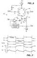
- FIG. 7is a view for explaining timing signals for the charge pump of FIG. 6 .
- FIG. 8is a detailed schematic view of a charge pump according to FIG. 6 .
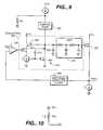
- FIG. 9is a view for explaining a current sink according to the invention.
- FIG. 10is a view for modeling a charge pump according to the invention.
- a switched capacitor ADCis shown in the form of a multi-stage pipelined ADC which includes multiple stages 11 through 12 each providing one or more bits of digital data to a digital correction circuit 15 which resolves the digital output from each stage into an overall digital output 16 that corresponds to an analog input 17 .
- Each stageis a switched capacitor circuit operating in response to clock signal ⁇ 1 for a sample phase and clock signal ⁇ 2 for an amplifying phase, and comparing an analog voltage input to thresholds based on reference signals Vrefp and Vrefn so as to produce the digital outputs as well as a residual analog signal.
- the residual analog signalis provided as input to a subsequent stage.
- Generator 20provides phase and timing signals including clock signals ⁇ 1 and ⁇ 2 .
- Generator 100generates reference voltages Vrefp and Vrefn for use by each of multiple stages 11 through 12 .
- generator 100generates reference voltage Vrefp which is output from the source terminal of follower 132 which is connected between voltage supply V+ and a current source 135 which in turn is connected to ground.
- follower 132is driven in negative feedback relationship to Vrefp through amplifier 134 whose reference is reference signal Vref.
- the negative feedback leg for amplifier 134is provided through filter 200 which is a switched capacitor filter operating in synchronism with phase and timing signals ⁇ 1 and ⁇ 2 so as to sample and filter reference voltage Vrefp during known quiescent periods of the ⁇ 1 sample phase and the ⁇ 2 amplification phase.
- the gate of follower 132is driven by current sink 300 , which accepts as its input the output from amplifier 134 .
- Current sink 300has an effective resistance which is low relative to other effective resistances in the circuit, thereby providing a low resistance path to sink current through follower 132 and thereby providing further immunization from the effects of high frequency noise.
- a voltage source for current sink 300is provided by charge pump 400 which provides an effectively higher voltage to current sink 300 than is otherwise available through supply voltage V+. Because of the higher effective voltage provided by charge pump 400 , it is possible to supply a reference voltage Vrefp which is very close to supply voltage V+, in spite of the existence of voltage drop Vgs across follower 132 .
- a complementary reference voltage generator 101is provided for Vrefn.
- Circuit 101involves components similar to switched capacitor filter 200 , current sink 300 and charge pump 400 , but operates those components in complementary relationship to those of generator 100 in correspondence to the reversed roles of ⁇ 1 and ⁇ 2 in the generator.
- switched capacitor filter 200Each of the components of switched capacitor filter 200 , current sink 300 and charge pump 400 , are described in more detail below.
- FIGS. 4A and 4Bare views for explaining switched capacitor filter 200 , which provides a final and settled value of the reference Vrefp signal for the feedback leg of amplifier 134 .
- One difference between FIGS. 4A and 4Binvolves the presence in FIG. 4A of current sink 300 and charge pump 400 , whereas those components are absent in the view of FIG. 4 B. These views are therefore intended to reinforce the notion that less than all three components (i.e., switched capacitor filter 200 , current sink 300 and charge pump 400 ) may be used in a generator for reference voltages, still with advantageous results.
- FIGS. 4C through 4EA source signal waveform is illustrated in each of these figures.
- a combination of switches ⁇ 1 and ⁇ 2e.g., switches driven by clocks ⁇ 1 and ⁇ 2 , respectively
- ⁇ 1 and ⁇ 2are non-overlapping clocks (e.g., as shown in FIG. 5 )
- FIG. 4Eillustrates the settling of the source signal.
- the source or excitation to such a switched capacitor filteris a glitch type signal for example V 1 , V 2 and V 3 , e.g., every T/2 seconds, as shown in FIG. 4F
- the height of the initial glitchis signal dependent.
- the average of this signal over one T period(e.g., low pass filtering the signal) can vary depending on signal value.
- ⁇ 1is preferably skewed such that the network RCp 2 does not see a glitch. Instead the network preferably sees a partially settled signal. As a result, the signal dependency is reduced to the feedback amplifier.
- filter 200includes switched capacitors Cp 1 and Cp 2 switched in accordance with clock signals ⁇ a and ⁇ b.
- Clock signals sa and ⁇ bare, in turn, timed relative to clock signal ⁇ 1 (sample) and clock signal ⁇ 2 (amplify) for ADC 10 .
- the value of Cp 2is much greater than Cp 1 .
- hais driven in synchronism with ⁇ 2 (amplification), but only after a time T 1 from when amplification commences.
- T 1The purpose for this delay T 1 is to ensure that Vrefp has recovered to a relatively stable value after any initial noise spikes generated during initial stages of amplification by multiple stages 11 through 12 .
- Cp 1samples the value of Vrefp, and holds that value after ⁇ a opens, during which time ⁇ b remains open.
- ⁇ bis driven in synchronism with ⁇ 1 (sample), or more precisely is driven out of synchronism with ⁇ a.
- ⁇ bcloses while ⁇ a is open, thereby allowing any charge accumulated on capacitor Cp 2 to mix with the charge newly acquired by capacitor Cp 1 , which reflects the current voltage level of Vrefp. It is the voltage accumulated on Cp 2 that is provided to the negative feedback leg of amplifier 134 , and that value is maintained even after ⁇ b opens.
- FIG. 5is a timing diagram showing operation of switched capacitor filter 200 .
- ⁇ 1 and ⁇ 2are sample and amplification signals, respectively, ⁇ a is driven in synchronism with amplification phase ⁇ 2 but commencing a short time T 1 after amplification begins, and ⁇ b is driven out of synchronism with ⁇ a and preferably in synchronism with ⁇ 1 .
- Vrefpis subjected to a voltage spike which is quickly accommodated by follower 132 so as to return to a nominal value.
- T 1is selected at design time so that it is timed for this nominal value.
- Vcp 1the voltage on capacitor Cp 1 (designated as Vcp 1 ) to follow any change in voltage level that might have occurred since the last closure of ⁇ a.
- ⁇ athen opens, followed by closure of ⁇ b, at which time the charge on capacitor Cp 1 is mixed with the charge currently stored on capacitor Cp 2 , thereby resulting in a change in voltage impressed across capacitor Cp 2 (designated as Vcp 2 ).
- Vcp 2the output value of Vrefp follows the change in voltage across capacitor Cp 2 by virtue of the negative feedback relationship caused by amplifier 134 .
- capacitor Cp 2is much greater than that for Cp 1 because the purpose of capacitor Cp 1 is to sample the voltage of Vrefp quickly, whereas the purpose of capacitor Cp 2 is to accumulate charge over a longer period of time and to provide a reasonable damping effect with good response time. This relationship is obtained with the previously-described 10:1 ratio between capacitances for Cp 2 and Cp 1 .
- the pole (p) of the cp 2 capacitoris p (Cp 1 /Cp 2 ) ⁇ f, where f equals 125 MHz, Cp 1 /Cp 2 equals 0.1, yielding a pole (p) of 12.5 MHz.
- capacitor Cp 2is filtered from high frequency noise injected by ADC 10 onto Vrefp, noise rejection from amplifier 134 (and onto follower 132 ) is greatly enhanced with respect to conventional feedback relationships. That noise rejection is reflected by the absence of any external capacitor such as Cext found in conventional voltage generators, because such an external capacitor is ordinarily not required.
- Charge pump 400is provided so as to produce an artificially elevated voltage level for follower 134 , so that it is possible to run the reference voltages Vrefp and Vrefn very close to supply voltage V+, in spite of the presence of the voltage drop Vgs from gate to source of follower 132 .
- FIG. 6shows the operational principles of charge pump 400 .
- the reference voltage Vrefp for ADC 10is generated from the source terminal of follower 132 which is connected between supply voltage V+ and a current source, which, in turn, is connected to ground.
- Vrefpis monitored through a negative feedback relationship to amplifier 134 whose reference is provided by a reference voltage Vret and whose feedback leg is connected to switched capacitor filter 200 .
- switched capacitor filter 200need not be supplied.
- the output of amplifier 134is provided to the gate of sink 135 , whose source is connected to the gate of follower 132 .
- Sink 135is provided to allow a sink of current from drain to gate of follower 132 , thereby providing an effectively low impedance looking inwardly toward sink 135 and amplifier 134 .
- the source terminal of sink 135is supplied by charge pump 400 .
- charge pump 400operates to artificially elevate source voltage V+ through capacitive switching and capacitive biasing, as explained more fully below.
- charge pump 400takes voltage source V+ through a current source and a biasing resistor R 3 and connects to two pairs of diagonally complementary switches S 1 and S 2 . These switches operate in connection with capacitors C 1 and C 1 a which are biased in synchronism with operation of switches S 1 and S 2 through biasing pulse Vpulse.
- switch S 1when switch S 1 is closed and in the absence of a biasing pulse on vpulse, capacitor C 1 charges to the level of supply voltage V+. Thereafter, switch S 1 closes and vpulse issues, thereby biasing the voltage at V 4 upwardly from V+ by the value of Vpulse.
- Vpulseis the same value as supply voltage V+, thereby effectively doubling the voltage at V 4 .
- switch S 2closes, thereby providing a voltage at V 5 which is elevated relative to supply voltage V+.
- switches S 1 and S 2occur in the right leg of charge pump 400 .
- switch S 2 in the left legis open
- switch Si in the right legis closed, thereby providing a biased voltage previously-impressed on capacitor C 1 a to voltage V 5 .
- This diagonally-complementary operation of switchesensures that the voltage at V 5 is artificially elevated relative to supply voltage V+.
- switches S 1 and S 2operate complementarily, and Vpulse operates in synchronism with closure of switch S 2 .
- the voltage from capacitor C 1 at V 4charges to the value of supply voltage V+.
- switch S 1 opens and switch S 2closes, and the voltage of capacitor C 1 is biased by issuance of vpulse, the voltage at V 4 increases to an elevated level relative to supply voltage V+ as signified by V++.
- Operation of current sink 135discharges capacitor C 1 , thereby resulting in a charge/discharge cycle signified at V 5 in FIG. 7 .
- the voltage V 5does not maintain its highest level at V++, it nevertheless maintains an average level which is elevated with respect to V+.
- VrefpBecause the voltage at V 5 is elevated relative to supply voltage V+, it is possible to operate Vrefp at a value very close to supply voltage V+, in spite of the gate-to-source voltage drop Vgs across follower 132 .
- switches S 1 and S 2In practice, however, it turns out to be difficult to build switches S 1 and S 2 because those switches must be turned on and off with voltages on the order of the supply voltage V+, yet must control voltages of values elevated with respect to V+.
- FIG. 8is a detailed schematic diagram for a practical implementation of charge pump 400 .
- switch S 1is formed by FET 401
- switch S 2is formed by a back-to-back connection of FET 402 and PMOSFET 404 .
- Switch S 1is driven inversely from Vpulse through inverter 405
- capacitor C 1is biased in coordination with Vpulse through dual inverters 406 .
- a helper capacitor C 3is switched and biased in coordination with capacitor C 1 through FET 407 which operates as a switch.
- capacitor C 1is charged to a voltage level corresponding to voltage supply V+.
- capacitor C 3is charged through FET 407 .
- switch S 1opens and capacitor C 1 is biased by the value of Vpulse.
- FET 407opens and capacitor C 3 is also biased by vpulse.
- Closure of switch S 2is a two-part operation.
- the first partsince the value of V 4 is approximately twice the value of reference voltage V+, it is not possible for FET 402 to turn on and allow capacitor C 1 to discharge to current sink 135 .
- FET 409is currently on and voltage at V 4 is currently the same as supply voltage V+.
- the supply voltagedrives the gate of PMOSFET 404 which therefore turns on and allows discharge of capacitor C 1 to current sink 135 .
- voltage at V 4decreases and will eventually decrease to a point where PMOS 404 can no longer remain on.
- capacitor C 2 and buffer 405are configured as a level shifter.
- Charge pump 400can be modeled as a resistor Rcp and a voltage supply that preferably supplies a voltage of approximately two times (e.g., 2V+) a voltage source (e.g., V+), as shown in FIG. 10.
- V 5Vrefp+Vgs
- FIG. 9is a detailed schematic view showing current sink 300 .
- the voltage V 5varies continuously according to the charge/discharge cycle shown at VS in FIG. 7 . Accordingly, if charge pump 400 is used, it is advantageous also to utilize a current sink 300 so as to reject noise generated by charge pump 400 in accordance with action of its switches S 1 and S 2 .
- current sink 300includes a low pass filter 301 which may include a simple RC circuit, which provides an input impedance (as viewed from the charge pump) that is low for high frequencies and higher for lower frequencies.
- the output of low pass filter 301is provided to follower 132 .
- the input to low pass filter 301is provided by a buffer composed of the combination of PETs 302 , 303 and 304 and capacitors C 1 and C 2 . Operation of this buffer is described in more detail below.
- the bufferprovides a buffered output based on the output of amplifier 134 and further provides an input impedance (as viewed from the charge pump) which is low for low frequencies and higher for high frequencies, thereby acting as a current sink for the output of charge pump 400 .
- the bufferis referred to generally at reference numeral 310 .
- buffer 310At low frequency operation of buffer 310 , the impedance thereof is influenced primarily by the transconductance of FET 302 since capacitor C 1 is essentially open. Specifically, at low frequencies the impedance of buffer 310 is the inverse of the transconductance of FET 302 , divided by the gain provided by FETs 303 and 304 . As a consequence, low frequency impedance of buffer 310 is lower than that of current sink 135 (FIG. 6) because of the amplifying effect of FETs 303 and 304 .
- capacitor C 1shorts. Consequently, in the absence of low pass is filter 301 , the input impendence of buffer 310 would increase to approximately the inverse of the transconductance of FET 302 (i.e., not divided by the gain of FETS 303 and 304 ). However, the presence of low pass filter 301 effectively ensures that at higher frequencies, the overall input impedance of current sink 300 remains low.
Landscapes
- Engineering & Computer Science (AREA)
- Power Engineering (AREA)
- Amplifiers (AREA)
Abstract
Description
Claims (36)
Priority Applications (1)
| Application Number | Priority Date | Filing Date | Title |
|---|---|---|---|
| US09/648,464US6396334B1 (en) | 2000-08-28 | 2000-08-28 | Charge pump for reference voltages in analog to digital converter |
Applications Claiming Priority (1)
| Application Number | Priority Date | Filing Date | Title |
|---|---|---|---|
| US09/648,464US6396334B1 (en) | 2000-08-28 | 2000-08-28 | Charge pump for reference voltages in analog to digital converter |
Publications (1)
| Publication Number | Publication Date |
|---|---|
| US6396334B1true US6396334B1 (en) | 2002-05-28 |
Family
ID=24600882
Family Applications (1)
| Application Number | Title | Priority Date | Filing Date |
|---|---|---|---|
| US09/648,464Expired - LifetimeUS6396334B1 (en) | 2000-08-28 | 2000-08-28 | Charge pump for reference voltages in analog to digital converter |
Country Status (1)
| Country | Link |
|---|---|
| US (1) | US6396334B1 (en) |
Cited By (15)
| Publication number | Priority date | Publication date | Assignee | Title |
|---|---|---|---|---|
| US6545628B1 (en) | 2000-08-22 | 2003-04-08 | Marvell International, Ltd. | Analog-to-digital converter with enhanced differential non-linearity |
| WO2004040760A1 (en)* | 2002-10-17 | 2004-05-13 | Infineon Technologies Ag | Circuit arrangement for regulating voltage |
| US6839015B1 (en) | 2002-12-06 | 2005-01-04 | Marvell International Ltd. | Low power analog to digital converter |
| US20050195003A1 (en)* | 2004-03-05 | 2005-09-08 | Soe Zaw M. | Charge pump circuit using active feedback controlled current sources |
| US20060012354A1 (en)* | 2004-07-13 | 2006-01-19 | Fujitsu Limited | Step-down circuit |
| US7071863B1 (en) | 2002-12-06 | 2006-07-04 | Marvell International Ltd. | Low power analog to digital converter having reduced bias during an inactive phase |
| US20070030037A1 (en)* | 2005-08-02 | 2007-02-08 | Wen-Chi Wang | Reference voltage generating circuit |
| US20070057701A1 (en)* | 2005-09-12 | 2007-03-15 | Analog Devices, Inc. | High-performance, low-noise reference generators |
| US7382305B1 (en) | 2007-02-26 | 2008-06-03 | Analog Devices, Inc. | Reference generators for enhanced signal converter accuracy |
| US20100259303A1 (en)* | 2009-04-09 | 2010-10-14 | Mediatek Inc. | Reference buffer circuit |
| US20120049951A1 (en)* | 2010-08-31 | 2012-03-01 | Texas Instruments Incorporated | High speed switched capacitor reference buffer |
| US20190214973A1 (en)* | 2018-01-10 | 2019-07-11 | Texas Instruments Incorporated | Low quiescent current load switch |
| US10879919B1 (en)* | 2019-07-26 | 2020-12-29 | Arm Limited | Voltage stabilizing techniques |
| USRE49018E1 (en)* | 2003-12-11 | 2022-04-05 | Mosaid Technologies Incorporated | Charge pump for PLL/DLL |
| CN115102390A (en)* | 2021-10-08 | 2022-09-23 | 上海南芯半导体科技股份有限公司 | Charge pump supporting ultra-low voltage charging |
Citations (16)
| Publication number | Priority date | Publication date | Assignee | Title |
|---|---|---|---|---|
| US5162668A (en)* | 1990-12-14 | 1992-11-10 | International Business Machines Corporation | Small dropout on-chip voltage regulators with boosted power supply |
| US5548205A (en) | 1993-11-24 | 1996-08-20 | National Semiconductor Corporation | Method and circuit for control of saturation current in voltage regulators |
| US5648718A (en) | 1995-09-29 | 1997-07-15 | Sgs-Thomson Microelectronics, Inc. | Voltage regulator with load pole stabilization |
| US5706240A (en)* | 1992-06-30 | 1998-01-06 | Sgs-Thomson Microelectronics S.R.L. | Voltage regulator for memory device |
| JPH1028053A (en) | 1996-07-10 | 1998-01-27 | Fujitsu General Ltd | A / D conversion error correction circuit |
| US5852359A (en) | 1995-09-29 | 1998-12-22 | Stmicroelectronics, Inc. | Voltage regulator with load pole stabilization |
| US5909109A (en) | 1997-12-15 | 1999-06-01 | Cherry Semiconductor Corporation | Voltage regulator predriver circuit |
| US5929616A (en) | 1996-06-26 | 1999-07-27 | U.S. Philips Corporation | Device for voltage regulation with a low internal dissipation of energy |
| WO1999048296A1 (en) | 1998-03-16 | 1999-09-23 | Intertrust Technologies Corporation | Methods and apparatus for continuous control and protection of media content |
| US6011666A (en) | 1996-12-16 | 2000-01-04 | Fujitsu Limited | Disk unit and portable electronic equipment |
| EP0982732A1 (en) | 1998-08-24 | 2000-03-01 | Saehan Information Systems Inc. | Portable MP3 player having various functions |
| US6061306A (en) | 1999-07-20 | 2000-05-09 | James Buchheim | Portable digital player compatible with a cassette player |
| EP0999549A2 (en) | 1998-11-02 | 2000-05-10 | Telian A/V Systems | MP3 car player |
| US6084387A (en) | 1998-02-03 | 2000-07-04 | Nec Corporation | Power source circuit for generating positive and negative voltage sources |
| US6184746B1 (en)* | 1999-08-13 | 2001-02-06 | Advanced Micro Devices, Inc. | PLL power supply filter (with pump) having a wide voltage range and immunity to oxide overstress |
| US6194887B1 (en)* | 1998-11-06 | 2001-02-27 | Nec Corporation | Internal voltage generator |
- 2000
- 2000-08-28USUS09/648,464patent/US6396334B1/ennot_activeExpired - Lifetime
Patent Citations (16)
| Publication number | Priority date | Publication date | Assignee | Title |
|---|---|---|---|---|
| US5162668A (en)* | 1990-12-14 | 1992-11-10 | International Business Machines Corporation | Small dropout on-chip voltage regulators with boosted power supply |
| US5706240A (en)* | 1992-06-30 | 1998-01-06 | Sgs-Thomson Microelectronics S.R.L. | Voltage regulator for memory device |
| US5548205A (en) | 1993-11-24 | 1996-08-20 | National Semiconductor Corporation | Method and circuit for control of saturation current in voltage regulators |
| US5648718A (en) | 1995-09-29 | 1997-07-15 | Sgs-Thomson Microelectronics, Inc. | Voltage regulator with load pole stabilization |
| US5852359A (en) | 1995-09-29 | 1998-12-22 | Stmicroelectronics, Inc. | Voltage regulator with load pole stabilization |
| US5929616A (en) | 1996-06-26 | 1999-07-27 | U.S. Philips Corporation | Device for voltage regulation with a low internal dissipation of energy |
| JPH1028053A (en) | 1996-07-10 | 1998-01-27 | Fujitsu General Ltd | A / D conversion error correction circuit |
| US6011666A (en) | 1996-12-16 | 2000-01-04 | Fujitsu Limited | Disk unit and portable electronic equipment |
| US5909109A (en) | 1997-12-15 | 1999-06-01 | Cherry Semiconductor Corporation | Voltage regulator predriver circuit |
| US6084387A (en) | 1998-02-03 | 2000-07-04 | Nec Corporation | Power source circuit for generating positive and negative voltage sources |
| WO1999048296A1 (en) | 1998-03-16 | 1999-09-23 | Intertrust Technologies Corporation | Methods and apparatus for continuous control and protection of media content |
| EP0982732A1 (en) | 1998-08-24 | 2000-03-01 | Saehan Information Systems Inc. | Portable MP3 player having various functions |
| EP0999549A2 (en) | 1998-11-02 | 2000-05-10 | Telian A/V Systems | MP3 car player |
| US6194887B1 (en)* | 1998-11-06 | 2001-02-27 | Nec Corporation | Internal voltage generator |
| US6061306A (en) | 1999-07-20 | 2000-05-09 | James Buchheim | Portable digital player compatible with a cassette player |
| US6184746B1 (en)* | 1999-08-13 | 2001-02-06 | Advanced Micro Devices, Inc. | PLL power supply filter (with pump) having a wide voltage range and immunity to oxide overstress |
Non-Patent Citations (14)
| Title |
|---|
| Bhupendra K. Ahuja, "An Improved Frequency Compensation Technique for CMOS Operational Amplifiers", IEEE Journal of Solid-State Circuits, vol. SC-18, No. 6, Dec. 1983, pp. 629-633. |
| Curtis Settles, "DSP-augmented CPU cores promise performance boost for ultra-compact drives", Data Storage, May 2000, pp. 35-38. |
| Paul C. Yu, et al., "A 2.5-V, 12-b, 5-Msample/s Pipelined CMOS ADC," IEEE Journal of Solid-State Circuits, vol., 31, No. 12, Dec. 1996, pp. 1854-61. |
| Quantum Online / Inside Hard Disk Drives, "Part 2-A Closer Look at Hard Disk Drives"; "Chapter 3-Inside Hard Disk Drives-How They Work", Jun. 7, 2000. |
| Quantum Online / Recent Technological Developments, "Chapter 4-The Impact of Leading-Edge Technology on Mass Storage", Jun. 7, 2000. |
| Sehat Sutarja and Paul R. Gray, "A Pipelined 13-bit, 250-ks/s, 5-V Analog-to-Digital Converter", IEEE Journal of Solid-State Circuits, vol. 23, No. 6, Dec. 1988, pp. 1316-1323. |
| Stephen H. Lewis and Paul R. Gray, "A Pipelined 5-Msample/s 9-bit Analog-to-Digital Converter", IEEE Journal of Solid-State Circuits, vol. SC-22, No. 6, Dec. 1987, pp. 954-961. |
| Stephen H. Lewis, "Optimizing the Stage Resolution in Pipelined, Multistage, Analog-to-Digital Converters for Video-Rate Applications", IEEE Transactions on Circuits and Systems-II: Analog and Digital Signal Processing, vol. 30, No. 8, Aug. 1992, pp 516-523. |
| Stephen H. Lewis, et al., "A 10-b 20-Msample/s Analog-to-Digital Converter", IEEE Journal of Solid-State Circuits, vol. 27, No. 3, Mar. 1992, pp. 351-358. |
| Stephen H. Lewis, et al., "Indirect Testing of Digital-Correction Circuits in Analog-to-Digital Converters with Redundancy," IEEE Transactions on Circuits and Systems-II: Analog and Digital Signal Processing, vol. 42, No. 7, Jul. 1995, pp. 437-445. |
| U.S. application No. 09/643,819, Aram, filed Aug. 22, 2000. |
| U.S. application No. 09/648,462, Aram et al., filed Aug. 28, 2000. |
| U.S. application No. 09/648,770, Aram et al., filed Aug. 28, 2000. |
| U.S. application No. 09/654,392, Aram, filed Sep. 1, 2000. |
Cited By (27)
| Publication number | Priority date | Publication date | Assignee | Title |
|---|---|---|---|---|
| US6545628B1 (en) | 2000-08-22 | 2003-04-08 | Marvell International, Ltd. | Analog-to-digital converter with enhanced differential non-linearity |
| US7042281B2 (en)* | 2002-10-17 | 2006-05-09 | Infineon Technologies Ag | Circuit arrangement for voltage regulation |
| WO2004040760A1 (en)* | 2002-10-17 | 2004-05-13 | Infineon Technologies Ag | Circuit arrangement for regulating voltage |
| US20050243623A1 (en)* | 2002-10-17 | 2005-11-03 | Infineon Technologies Ag | Circuit arrangement for voltage regulation |
| US6839015B1 (en) | 2002-12-06 | 2005-01-04 | Marvell International Ltd. | Low power analog to digital converter |
| US6967610B1 (en) | 2002-12-06 | 2005-11-22 | Marvell International Ltd. | Low power bit and one-half analog to digital converter |
| US7071863B1 (en) | 2002-12-06 | 2006-07-04 | Marvell International Ltd. | Low power analog to digital converter having reduced bias during an inactive phase |
| USRE49018E1 (en)* | 2003-12-11 | 2022-04-05 | Mosaid Technologies Incorporated | Charge pump for PLL/DLL |
| US20050195003A1 (en)* | 2004-03-05 | 2005-09-08 | Soe Zaw M. | Charge pump circuit using active feedback controlled current sources |
| US6980046B2 (en)* | 2004-03-05 | 2005-12-27 | Wionics Research | Charge pump circuit using active feedback controlled current sources |
| US20060012354A1 (en)* | 2004-07-13 | 2006-01-19 | Fujitsu Limited | Step-down circuit |
| US7554305B2 (en)* | 2004-07-13 | 2009-06-30 | Fujitsu Microelectronics Limited | Linear regulator with discharging gate driver |
| US20070030037A1 (en)* | 2005-08-02 | 2007-02-08 | Wen-Chi Wang | Reference voltage generating circuit |
| US7456769B2 (en)* | 2005-08-02 | 2008-11-25 | Realtek Semiconductor Corp. | Reference voltage generating circuit |
| US7215182B2 (en) | 2005-09-12 | 2007-05-08 | Analog Devices, Inc. | High-performance, low-noise reference generators |
| US20070057701A1 (en)* | 2005-09-12 | 2007-03-15 | Analog Devices, Inc. | High-performance, low-noise reference generators |
| US7382305B1 (en) | 2007-02-26 | 2008-06-03 | Analog Devices, Inc. | Reference generators for enhanced signal converter accuracy |
| US20100259303A1 (en)* | 2009-04-09 | 2010-10-14 | Mediatek Inc. | Reference buffer circuit |
| US8222927B2 (en) | 2009-04-09 | 2012-07-17 | Mediatek Inc. | Reference buffer circuit |
| US20120049951A1 (en)* | 2010-08-31 | 2012-03-01 | Texas Instruments Incorporated | High speed switched capacitor reference buffer |
| US20190214973A1 (en)* | 2018-01-10 | 2019-07-11 | Texas Instruments Incorporated | Low quiescent current load switch |
| US10432175B2 (en)* | 2018-01-10 | 2019-10-01 | Texas Instruments Incorporated | Low quiescent current load switch |
| US10868521B2 (en)* | 2018-01-10 | 2020-12-15 | Texas Instruments Incorporated | Low quiescent current load switch |
| EP3738207A4 (en)* | 2018-01-10 | 2021-07-28 | Texas Instruments Incorporated | LOAD SWITCH WITH LOW STANDBY CURRENT |
| US10879919B1 (en)* | 2019-07-26 | 2020-12-29 | Arm Limited | Voltage stabilizing techniques |
| CN115102390A (en)* | 2021-10-08 | 2022-09-23 | 上海南芯半导体科技股份有限公司 | Charge pump supporting ultra-low voltage charging |
| CN115102390B (en)* | 2021-10-08 | 2024-05-10 | 上海南芯半导体科技股份有限公司 | Charge pump supporting ultra-low voltage charging |
Similar Documents
| Publication | Publication Date | Title |
|---|---|---|
| US6417725B1 (en) | High speed reference buffer | |
| US6396334B1 (en) | Charge pump for reference voltages in analog to digital converter | |
| US10250131B2 (en) | Low-noise high efficiency bias generation circuits and method | |
| US8054141B2 (en) | Method and circuit for cancelling out comparator-delay in the relaxation oscillator | |
| Baschirotto et al. | A 1-V 1.8-MHz CMOS switched-opamp SC filter with rail-to-rail output swing | |
| US8994452B2 (en) | Low-noise high efficiency bias generation circuits and method | |
| US6362683B1 (en) | Break-before-make distortion compensation for a digital amplifier | |
| JP2804764B2 (en) | Amplifier device switchable between operating modes | |
| US6400214B1 (en) | Switched capacitor filter for reference voltages in analog to digital converter | |
| US11165396B2 (en) | Amplifier arrangement and sensor arrangement with such amplifier arrangement | |
| SG188739A1 (en) | Low power high resolution sensor interface | |
| US5302863A (en) | CMOS peak amplitude detector | |
| US5631603A (en) | Offset cancellation for differential amplifiers | |
| JP4785801B2 (en) | Class D amplifier | |
| US6801080B1 (en) | CMOS differential input buffer with source-follower input clamps | |
| US20070109043A1 (en) | Operational amplifier with zero offset | |
| Baschirotto | A low-voltage sample-and-hold circuit in standard CMOS technology operating at 40 Ms/s | |
| JPH08279750A (en) | Comparator,a/d converter,and controlling method for adaptable switch to the comparator | |
| KR100767581B1 (en) | Differential type operational amplifier | |
| US7345528B2 (en) | Method and apparatus for improved clock preamplifier with low jitter | |
| US6573851B2 (en) | Offset compensated comparing amplifier | |
| US6696884B1 (en) | Method and apparatus to achieve long time constants with a small MOS gate capacitor | |
| US6781450B1 (en) | Low-frequency auto-zeroed amplifier | |
| US6424208B1 (en) | Switched capacitor filter with integrated voltage multiplier | |
| US6630898B1 (en) | Low voltage, unit delay quantizer with feedforward auto-zero mechanism |
Legal Events
| Date | Code | Title | Description |
|---|---|---|---|
| AS | Assignment | Owner name:MARVELL SEMICONDUCTOR, INC., CALIFORNIA Free format text:ASSIGNMENT OF ASSIGNORS INTEREST;ASSIGNOR:ARAM, FARBOD;REEL/FRAME:011136/0253 Effective date:20000824 Owner name:MARVELL TECHNOLOGY GROUP, LTD., BERMUDA Free format text:ASSIGNMENT OF ASSIGNORS INTEREST;ASSIGNOR:MARVELL SEMICONDUCTOR, INC.;REEL/FRAME:011136/0263 Effective date:20000825 | |
| AS | Assignment | Owner name:MARVELL INTERNATIONAL LTD., BERMUDA Free format text:ASSIGNMENT OF ASSIGNORS INTEREST;ASSIGNOR:MARVELL TECHNOLOGY GROUP, LTD.;REEL/FRAME:011534/0124 Effective date:20010119 | |
| STCF | Information on status: patent grant | Free format text:PATENTED CASE | |
| FPAY | Fee payment | Year of fee payment:4 | |
| FPAY | Fee payment | Year of fee payment:8 | |
| FPAY | Fee payment | Year of fee payment:12 | |
| AS | Assignment | Owner name:CAVIUM INTERNATIONAL, CAYMAN ISLANDS Free format text:ASSIGNMENT OF ASSIGNORS INTEREST;ASSIGNOR:MARVELL INTERNATIONAL LTD.;REEL/FRAME:052918/0001 Effective date:20191231 | |
| AS | Assignment | Owner name:MARVELL ASIA PTE, LTD., SINGAPORE Free format text:ASSIGNMENT OF ASSIGNORS INTEREST;ASSIGNOR:CAVIUM INTERNATIONAL;REEL/FRAME:053475/0001 Effective date:20191231 |