US6396205B1 - Nonspecular visual display and method - Google Patents
Nonspecular visual display and methodDownload PDFInfo
- Publication number
- US6396205B1 US6396205B1US09/215,522US21552298AUS6396205B1US 6396205 B1US6396205 B1US 6396205B1US 21552298 AUS21552298 AUS 21552298AUS 6396205 B1US6396205 B1US 6396205B1
- Authority
- US
- United States
- Prior art keywords
- display
- display elements
- elements
- visual display
- substrate
- Prior art date
- Legal status (The legal status is an assumption and is not a legal conclusion. Google has not performed a legal analysis and makes no representation as to the accuracy of the status listed.)
- Expired - Fee Related
Links
- 230000000007visual effectEffects0.000titleclaimsabstractdescription35
- 238000000034methodMethods0.000titleclaimsdescription14
- 239000000463materialSubstances0.000claimsabstractdescription41
- 238000005538encapsulationMethods0.000claimsabstractdescription34
- 239000010410layerSubstances0.000claimsdescription59
- 239000000758substrateSubstances0.000claimsdescription15
- 239000002356single layerSubstances0.000claimsdescription7
- 239000004014plasticizerSubstances0.000claimsdescription6
- 150000001875compoundsChemical class0.000claims3
- 239000003094microcapsuleSubstances0.000claims3
- 230000004313glareEffects0.000abstractdescription11
- 230000001681protective effectEffects0.000description9
- 230000005684electric fieldEffects0.000description5
- 239000012530fluidSubstances0.000description5
- 239000002245particleSubstances0.000description5
- 229920001971elastomerPolymers0.000description3
- 239000000806elastomerSubstances0.000description3
- 239000011521glassSubstances0.000description3
- 239000004033plasticSubstances0.000description3
- 238000004519manufacturing processMethods0.000description2
- 239000012780transparent materialSubstances0.000description2
- 239000000853adhesiveSubstances0.000description1
- 230000001070adhesive effectEffects0.000description1
- 239000011248coating agentSubstances0.000description1
- 238000000576coating methodMethods0.000description1
- 238000000151depositionMethods0.000description1
- 239000005357flat glassSubstances0.000description1
- 238000010438heat treatmentMethods0.000description1
- 238000010348incorporationMethods0.000description1
- 239000007788liquidSubstances0.000description1
- 239000004973liquid crystal related substanceSubstances0.000description1
- 230000007246mechanismEffects0.000description1
- 230000004048modificationEffects0.000description1
- 238000012986modificationMethods0.000description1
- 238000012856packingMethods0.000description1
- 238000007788rougheningMethods0.000description1
- 239000007787solidSubstances0.000description1
Images


Classifications
- G—PHYSICS
- G02—OPTICS
- G02B—OPTICAL ELEMENTS, SYSTEMS OR APPARATUS
- G02B1/00—Optical elements characterised by the material of which they are made; Optical coatings for optical elements
- G02B1/10—Optical coatings produced by application to, or surface treatment of, optical elements
- G02B1/11—Anti-reflection coatings
- G—PHYSICS
- G02—OPTICS
- G02B—OPTICAL ELEMENTS, SYSTEMS OR APPARATUS
- G02B26/00—Optical devices or arrangements for the control of light using movable or deformable optical elements
- G02B26/02—Optical devices or arrangements for the control of light using movable or deformable optical elements for controlling the intensity of light
- G02B26/026—Optical devices or arrangements for the control of light using movable or deformable optical elements for controlling the intensity of light based on the rotation of particles under the influence of an external field, e.g. gyricons, twisting ball displays
Definitions
- the inventionrelates to visual displays. More particularly, the invention relates to nonspecular, reusable, paper-like, gyricon or twisting-particle type or other visual displays and method.
- Paperis a preferred medium to present and display text and images.
- a reason for paper being a preferred mediumis the many advantages that are realized with the use of paper as a display medium.
- paperis thin, lightweight, portable, flexible, foldable, cost efficient, high contrast, reusable, basically permanent, and can easily be configured into a multitude of shapes.
- paperdoes not have any limitations on size, other than practicality, and as such, can be used as display media such as, for example, sticky notes or such, maps and billboards, to name a few.
- paperis capable of maintaining a displayed image without the need for a power source, such as, for example, batteries and other such stored energy sources.
- papercan be read in ambient light, as well as marked upon with any number of implements, such as, for example, a pen, pencil, paintbrush, printers, photocopiers, and the like.
- paperdoes not suffer from specular reflection.
- specular reflectionthere is no mirror-like or direct reflection of light from a light source off the viewed surface of paper like that found in conventional cathode-ray tube (CRT) displays.
- Specularly reflected light on a television or computer screenfor example, produces an annoying glare such that a viewer must reposition his head to not look at the direct reflection of light.
- the viewed surface of paperis usually rough, for example, light is scattered diffusely by the viewed surface so that the viewer can look directly at the paper in a comfortable manner.
- paperhas many advantages as a display medium
- paperis not well suited for real-time display purposes.
- Real-time imagery from computer, video, and other sourcescannot be displayed by means other than, for example, a CRT display or a liquid-crystal display (LCD).
- LCDliquid-crystal display
- most real-time display medialack many of the desirable advantages of paper, such as, for example, being lightweight, thin, portable, physically flexible, and the ability to retain a displayed image in a stable manner without a power source.
- most real-time display mediause a flat glass display surface, such media specularly reflect light and produce an annoying glare.
- attemptshave been made to combine the desirable qualities of paper with those of real-time display media in order to provide a display that offers the best of both worlds.
- One such displayis electric paper.
- electric papercan be written on and erased, can be read in ambient light, and can retain information in the absence of an electric field or other external retaining force.
- electric papercan be made in the form of a lightweight, flexible, durable sheet that can be folded or rolled into tubular form about any axis and conveniently placed into a shirt or coat pocket, and then later retrieved, restraightened, and read substantially without loss of information.
- electric paperpossibly can be used to display imagery in motion.
- electric paperis adaptable for use in computer systems, television, signs and a host of other applications within office, industrial and domestic settings.
- a gyricon displayalso called a twisting-element display, rotary element display, particle display, dipolar particle light valve, and the like.
- a gyricon displayincludes a plurality of optically anisotropic particles, such as, for example, spheres, each of which can be selectively rotated to present a desired image to an observer.
- a gyricon displaycan incorporate rotational elements each having two distinct halves, e.g., one half may be black, while the other half is white.
- the rotational elementsare embedded in a sheet of optically transparent material that contains a plurality of cavities and is permeated by an optically transparent dielectric fluid.
- the fluid-filled cavitiesaccommodate the rotational elements, one element per cavity, so as to prevent the elements from migrating within the sheet.
- Each elementhas a distinct electrical characteristic so that the elements are electrically as well as optically anisotropic.
- an elementcan be selectively rotated within its respective cavity by application of an electric field, so as to present either the black or the white half to an observer viewing the surface of the sheet, for example.
- electric paper displaysalso typically have a substantially transparent flat surface that subjects a viewer to the annoying glare associated with the specular reflected which prevents the viewer from seeing the diffuse light scattered off the surface of the rotational elements.
- the inventionprovides a nonspecular visual display and method in which the display achieves an appearance much like paper.
- the inventionuses a substantially thin encapsulation layer that conforms to the shape of elements in the display.
- the conformal layer of encapsulation material of the displayachieves a paper-like appearance because there is no specular reflection of light produced by the conformal layer. In other words, light is diffusely reflected by the surface of the conformal layer.
- microencapulated display elementsare formed on a substrate. Since there is no top layer covering the display elements, ambient light is not specularly reflected by the display.
- FIG. 1is a cross section of a conventional gyricon display
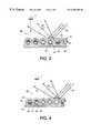
- FIG. 2is a cross section of an embodiment of a visual display in accordance with the invention.
- FIG. 3is a cross section of another embodiment of the visual display in accordance with the invention.
- FIG. 4is a cross section of another embodiment of the visual display in accordance with the invention.
- FIG. 5is a cross section of yet another embodiment of the visual display in accordance with the invention.
- U.S. Pat. No. 4,126,854describes a twisting element display panel 10 shown in FIG. 1 .
- U.S. Pat. No. 4,143,103discloses a method of making the twisting element display 10 .
- the display 10 shown in these patentsinitially has a plurality of display elements 11 mixed with an uncured, optically transparent material 12 , such as, for example, an elastomer.
- the uncured material 12is then cured, thereby providing a solid display panel 13 in which the display elements 11 are fixed so that the display elements 11 cannot rotate or move translationally.
- the display panel 13is placed in a dielectric liquid plasticizer 14 .
- the material 12absorbs the plasticizer 14 so that the display panel 13 swells and cavities 15 are formed around each of the display elements 11 .
- the cavities 15are filled with the plasticizer 14 allowing rotation, if desired, of the display elements 11 , while allowing essentially no translational movement of the display elements 11 .
- the plasticized materialis then bonded between two protective sheets of plastic or glass 16 and 17 . One or both of the sheets 16 and 17 is transparent.
- a number of addressing mechanismsknown in the art are used to cause the display elements 11 to rotate in conjunction with an image based electric field pattern (not shown).
- the electric field patternmay be accomplished by, for example, depositing a charge on the surface of the display 10 with a stylus or by adding a transparent electrode pattern to the top or bottom surface of the display 10 , which is electrically addressed. In all such cases, the difference in electrical charge between the differently colored portions of the display elements 11 cause each element 11 to rotate differently in response to the applied electric fields, as depicted in FIGS. 1-5, thereby forming ran image like pattern.
- the invention described hereinimproves visual displays by substantially eliminating the glare associated with specular reflection by applying a substantially thin conformal layer of encapsulation material across a surface of display elements near the upper surface of the display panel.
- the inventive structureachieves a visual display 20 having an appearance very much like paper.
- a plurality of display elements 21are disposed on a base layer 22 of encapsulation material such that a top layer of the display elements 21 are partially immersed in the material 22 .
- a substantially thin conformal layer 23 of encapsulation materialis deposited over an exposed surface of the display elements 21 .
- the thickness of the conformal layer 23 of encapsulation materialmust be substantially thinner than the width of the display elements 21 so that the conformal layer 23 does not planarize, but instead conforms to the shape of the display elements 21 .
- the conformal layer 23should have a thickness of 5 microns or less.
- the conformal layer 23 of encapsulation materialis optically transparent. It should also be noted that the encapsulation material can be an elastomer, for example.
- the encapsulation materialis swelled with the plasticizer 24 in a similar manner as described above so the display elements 21 are able to rotate in their cavities 25 as in the conventional display 10 .
- the plasticized materialcan be bonded to a protective bottom sheet 26 a and/or protective top sheet 26 b of plastic, glass or the like on the top and/or bottom of the display 20 . If a protective top sheet 26 b is provided over the top of the conformal layer 23 , the protective top sheet 26 b is preferably conformal, otherwise, the sheet 26 b will specularly reflect light.
- the conformal layer 23 of encapsulation materialproduces a paper-like appearance of the inventive display 20 . Furthermore, the conformal surface of the display 20 does not produce any specular reflection. Instead, light 27 incident upon the display 20 diffusely reflects off the conformal layer 23 of the encapsulation material 22 because the conformal layer 23 of the encapsulation material forms a rough upper surface. As such, the diffusely reflected light 28 is scattered off the conformal layer 23 producing no glare and allowing a viewer to comfortably view the display 20 at I without having to reposition his head.
- FIG. 3shows another embodiment of the display 30 according to the invention where, as disclosed in U.S. Pat. No. 5,604,027, the display 30 can have rotating display elements 31 that use a separate encapsulating shell 36 to enclose both the rotating display elements 31 and a sufficient thickness of the dielectric fluid 34 to allow free rotation of the rotating display elements 31 in their cavities 35 .
- the display elements 31are disposed on a base layer 32 of encapsulation material and packed close together in a monolayer to provide excellent brightness characteristics such that each display element 31 is partially immersed in the material 32 and has an exposed top surface.
- a substantially thin conformal layer 33 of encapsulation materialis deposited over the exposed surface of the display elements 31 similar to the display depicted in FIG.
- the conformal layer 33conforms to the encapsulating shells 36 so light 38 incident upon the display 30 diffusely reflects off the conformal layer 33 of the encapsulation material.
- the diffusely reflected light 39is scattered off the conformal layer 33 producing no glare and allowing a viewer to comfortably view the display 30 at I without having to reposition his head.
- the plasticized materialcan be bonded to a protective sheet 37 of plastic, glass or the like as explained above for the display 20 .
- FIG. 4shows another embodiment of the display 40 according to the invention where the display 40 has separate encapsulating shells 46 bonded directly to the protective sheet 47 without being placed in a base layer 32 of encapsulating material as shown in FIG. 3 .
- the shells 46are bonded directly to the sheet 47 by any known or subsequently developed adhesive, by heating, or any known or subsequently developed bonding technique.
- a substantially thin conformal layer 43 of encapsulation materialis deposited over the encapsulating shells 46 such that the conformal layer 43 conforms to the encapsulating shells 46 . Therefore, light 48 incident upon the display 40 diffusely reflects off the conformal layer 43 .
- the display elements 41 and dielectric fluid 44 within cavities 45are contained in the shells 46 .
- the diffusely reflected light 49is scattered off the conformal layer 43 producing no glare and allowing a viewer to comfortably view the display 40 at I without having to reposition his head.
- FIG. 5shows yet another embodiment of the display 50 according to the invention where the encapsulated shells 56 are bonded directly to the protective sheet 57 without an encapsulation layer.
- the display elements 51 and dielectric fluid 54 within cavities 55are contained in the shells 56 . Since the encapsulated shells 56 have a similar shape (conformal) as the rotating display elements 21 , 31 , 41 , and 51 , light 58 incident upon the display 50 diffusely reflects off the non-flat surface of the shells 56 .
- the diffusely reflected light 59is scattered off the shells 56 producing no glare and allowing a viewer to comfortably view the display 50 at I without having to reposition his head.
- the display elements 21 , 31 , 41 , and 51 discussed aboveare depicted in FIGS. 2-5 as being spherical, it is understood that the display elements 21 , 31 , 41 , and 51 are not limited to the illustrated configuration, but are represented as such merely for explanatory purposes.
- the display 20 , 30 , 40 , and 50 according to the invention and as disclosed in U.S. patent application Ser. No. 08/960,865the display can have cylindrical, rather than spherical display elements.
- the display elementscan be bichromal or polychromal cylinders aligned parallel to one another. As evident by the displays 30 , 40 , and 50 shown in FIGS. 3-5, such a configuration provides excellent brightness characteristics as well as relative ease of manufacture.
- the displays 20 , 30 , 40 , and 50can have rotating cylindrical elements with multiple chromatic values.
- each layer of colorshould appear as complete to an observer as possible.
- Several methodsare known in the art for obtaining optimum area coverage. For example, such packing methods are described in U.S. patent application Ser. No. 08/713,935; U.S. patent application Ser. No. 08/713,936; U.S. patent application Ser. No. 08/716,675; and U.S. patent application Ser. No. 08/713,325.
- the display 20 , 30 , 40 , and 50 in any of the above embodimentscan be an electrophoretic display device, such as that described in the article entitled “A Stylus Writable Electrophoretic Display Device” authored by A. Chiang, D. Curry and M. Zarzychi and published in SID Digest 79, pp. 44-45, which is incorporated herein by reference.
- the conformal layerconforms to an exposed outer surface of electrophoretic display elements, which can be sacs or other such elements so that light incident upon such a display diffusely reflects off the conformal layer of the encapsulation material.
- one or both of the protective sheet 26 a , 26 b , 37 , 47 , and 57 and the conformal layer 23 , 33 and 43 of encapsulation materialcan have a conductive coating or include any other conductive patterns, layers or elements for addressing the display elements 21 , 31 , 41 , and 51 . Accordingly, the specific embodiments of the invention as set forth herein are intended to be illustrative, not limiting. Various changes may be made without departing from the spirit and scope of the invention as set forth in the following claims.
Landscapes
- Physics & Mathematics (AREA)
- General Physics & Mathematics (AREA)
- Optics & Photonics (AREA)
- Health & Medical Sciences (AREA)
- Life Sciences & Earth Sciences (AREA)
- Molecular Biology (AREA)
- Devices For Indicating Variable Information By Combining Individual Elements (AREA)
- Electrochromic Elements, Electrophoresis, Or Variable Reflection Or Absorption Elements (AREA)
Abstract
Description
Claims (29)
Priority Applications (2)
| Application Number | Priority Date | Filing Date | Title |
|---|---|---|---|
| US09/215,522US6396205B1 (en) | 1998-12-18 | 1998-12-18 | Nonspecular visual display and method |
| JP35357599AJP4527221B2 (en) | 1998-12-18 | 1999-12-13 | Non-mirror display |
Applications Claiming Priority (1)
| Application Number | Priority Date | Filing Date | Title |
|---|---|---|---|
| US09/215,522US6396205B1 (en) | 1998-12-18 | 1998-12-18 | Nonspecular visual display and method |
Publications (1)
| Publication Number | Publication Date |
|---|---|
| US6396205B1true US6396205B1 (en) | 2002-05-28 |
Family
ID=22803313
Family Applications (1)
| Application Number | Title | Priority Date | Filing Date |
|---|---|---|---|
| US09/215,522Expired - Fee RelatedUS6396205B1 (en) | 1998-12-18 | 1998-12-18 | Nonspecular visual display and method |
Country Status (2)
| Country | Link |
|---|---|
| US (1) | US6396205B1 (en) |
| JP (1) | JP4527221B2 (en) |
Cited By (12)
| Publication number | Priority date | Publication date | Assignee | Title |
|---|---|---|---|---|
| US20020190936A1 (en)* | 1999-09-28 | 2002-12-19 | Brother International Corporation | Methods and apparatus for subjecting an element to an electrical filed |
| US6661563B2 (en)* | 2000-01-31 | 2003-12-09 | Fujitsu Limited | Sheet-shaped display, sphere-like resin body, and micro-capsule |
| US20040030111A1 (en)* | 2002-06-19 | 2004-02-12 | Turner Douglas H. | Oligonucleotide directed misfolding of RNA |
| US20050244618A1 (en)* | 2004-04-30 | 2005-11-03 | Brian Gobrogge | Islanded pattern for printing on readdressable media |
| US20050289015A1 (en)* | 2000-05-17 | 2005-12-29 | Hunter Charles E | System and method permitting merchants to use electronic billboard displays to carry advertisements for products that can be purchased through a universal, automated order processing system |
| US7015875B2 (en)* | 2001-06-29 | 2006-03-21 | Novus Partners Llc | Dynamic device for billboard advertising |
| US7088352B2 (en) | 2002-06-19 | 2006-08-08 | Novus Partners Llc | Dynamic device and method for dispensing machines |
| US7098870B2 (en)* | 2001-06-29 | 2006-08-29 | Novus Partners Llc | Advertising method for dynamic billboards |
| US7098869B2 (en) | 2001-06-29 | 2006-08-29 | Novus Partners Llc | Business method for billboard advertising |
| US7895088B2 (en) | 1999-04-28 | 2011-02-22 | Novus Partners, Llc | System permitting the display of video or still image content on selected displays of an electronic display network according to customer dictates |
| US20110254427A1 (en)* | 2010-04-19 | 2011-10-20 | Samsung Electro-Mechanics Co., Ltd. | Color electronic paper display device and method for manufacturing the same |
| US8736948B2 (en) | 2013-03-01 | 2014-05-27 | Kedrick F. Brown | Electromechanical billboard |
Citations (36)
| Publication number | Priority date | Publication date | Assignee | Title |
|---|---|---|---|---|
| US2143946A (en)* | 1935-05-30 | 1939-01-17 | Hunter Frederick | Method of manufacturing signs and other display devices |
| US2326634A (en) | 1941-12-26 | 1943-08-10 | Minnesota Mining & Mfg | Reflex light reflector |
| US2354049A (en) | 1944-01-19 | 1944-07-18 | Minnesota Mining & Mfg | Backless reflex light reflector |
| US2354048A (en) | 1940-08-03 | 1944-07-18 | Minnesota Mining & Mfg | Flexible lenticular optical sheet |
| US2354018A (en) | 1940-08-03 | 1944-07-18 | Minnesota Mining & Mfg | Light reflector sheet |
| US2422256A (en)* | 1940-02-13 | 1947-06-17 | Minnesota Mining & Mfg | Flexible reflex reflecting film |
| US3567307A (en)* | 1966-12-02 | 1971-03-02 | Prismo Universal Corp | Reflective markers |
| FR2161301A5 (en) | 1971-11-19 | 1973-07-06 | Sobiepanek Janusz | |
| US3795435A (en) | 1969-05-09 | 1974-03-05 | Swarovski & Co | Reflex light reflection sheet and method for its manufacture |
| US3915771A (en) | 1974-03-04 | 1975-10-28 | Minnesota Mining & Mfg | Pavement-marking tape |
| US4082426A (en) | 1976-11-26 | 1978-04-04 | Minnesota Mining And Manufacturing Company | Retroreflective sheeting with retroreflective markings |
| US4104102A (en)* | 1975-02-24 | 1978-08-01 | Morgan Adhesives Company | Method of making a retroreflective laminate |
| USRE29742E (en) | 1973-11-05 | 1978-08-29 | Minnesota Mining And Manufacturing Company | Retroreflective protective helmet |
| US4117192A (en) | 1976-02-17 | 1978-09-26 | Minnesota Mining And Manufacturing Company | Deformable retroreflective pavement-marking sheet material |
| US4126854A (en) | 1976-05-05 | 1978-11-21 | Xerox Corporation | Twisting ball panel display |
| US4143103A (en) | 1976-05-04 | 1979-03-06 | Xerox Corporation | Method of making a twisting ball panel display |
| US4261653A (en) | 1978-05-26 | 1981-04-14 | The Bendix Corporation | Light valve including dipolar particle construction and method of manufacture |
| US4367920A (en) | 1979-10-01 | 1983-01-11 | Minnesota Mining And Manufacturing Company | Retroflective sheeting |
| US4438160A (en) | 1982-01-18 | 1984-03-20 | Sony Corporation | Method of making a rotary ball display device |
| US4511210A (en) | 1979-10-01 | 1985-04-16 | Minnesota Mining And Manufacturing Company | Retroreflective sheeting |
| US4569857A (en) | 1979-10-01 | 1986-02-11 | Minnesota Mining And Manufacturing Company | Retroreflective sheeting |
| US4678695A (en) | 1985-12-23 | 1987-07-07 | Minnesota Mining And Manufacturing Company | Encapsulated flattop retroreflective sheeting and method for producing the same |
| US4688900A (en) | 1984-03-19 | 1987-08-25 | Kent State University | Light modulating material comprising a liquid crystal dispersion in a plastic matrix |
| US4721649A (en) | 1985-05-08 | 1988-01-26 | Minnesota Mining And Manufacturing Company | Retroreflective sheeting |
| US4725494A (en) | 1982-09-02 | 1988-02-16 | Minnesota Mining And Manufacturing Co. | Retroreflective sheeting |
| US4810431A (en) | 1986-05-23 | 1989-03-07 | Ontario Research Foundation | Method of manufacturing plastic particles for a particle display |
| US4919521A (en) | 1987-06-03 | 1990-04-24 | Nippon Sheet Glass Co., Ltd. | Electromagnetic device |
| US5155607A (en) | 1990-03-16 | 1992-10-13 | Fuji Xerox Co., Ltd. | Optical modulation display device and display method using the same |
| US5251048A (en) | 1992-05-18 | 1993-10-05 | Kent State University | Method and apparatus for electronic switching of a reflective color display |
| US5262098A (en) | 1992-12-23 | 1993-11-16 | Xerox Corporation | Method and apparatus for fabricating bichromal balls for a twisting ball display |
| US5344594A (en) | 1991-10-29 | 1994-09-06 | Xerox Corporation | Method for the fabrication of multicolored balls for a twisting ball display |
| US5389945A (en) | 1989-11-08 | 1995-02-14 | Xerox Corporation | Writing system including paper-like digitally addressed media and addressing device therefor |
| US5469020A (en) | 1994-03-14 | 1995-11-21 | Massachusetts Institute Of Technology | Flexible large screen display having multiple light emitting elements sandwiched between crossed electrodes |
| US5604027A (en) | 1995-01-03 | 1997-02-18 | Xerox Corporation | Some uses of microencapsulation for electric paper |
| US5894367A (en)* | 1996-09-13 | 1999-04-13 | Xerox Corporation | Twisting cylinder display using multiple chromatic values |
| US6054208A (en)* | 1998-01-16 | 2000-04-25 | Avery Dennison Corporation | Film forming mixtures, image bearing films and image bearing retroreflective sheeting |
Family Cites Families (5)
| Publication number | Priority date | Publication date | Assignee | Title |
|---|---|---|---|---|
| JPS5427797A (en)* | 1977-08-03 | 1979-03-02 | Epson Corp | Photoreceptor indicator |
| JPS5667886A (en)* | 1979-11-08 | 1981-06-08 | Sony Corp | Display device and producing same |
| JPS5667887A (en)* | 1979-11-08 | 1981-06-08 | Sony Corp | Display unit and producing same |
| US4915482A (en)* | 1988-10-27 | 1990-04-10 | International Business Machines Corporation | Optical modulator |
| JP4006769B2 (en)* | 1996-11-11 | 2007-11-14 | 凸版印刷株式会社 | Display surface material |
- 1998
- 1998-12-18USUS09/215,522patent/US6396205B1/ennot_activeExpired - Fee Related
- 1999
- 1999-12-13JPJP35357599Apatent/JP4527221B2/ennot_activeExpired - Fee Related
Patent Citations (36)
| Publication number | Priority date | Publication date | Assignee | Title |
|---|---|---|---|---|
| US2143946A (en)* | 1935-05-30 | 1939-01-17 | Hunter Frederick | Method of manufacturing signs and other display devices |
| US2422256A (en)* | 1940-02-13 | 1947-06-17 | Minnesota Mining & Mfg | Flexible reflex reflecting film |
| US2354048A (en) | 1940-08-03 | 1944-07-18 | Minnesota Mining & Mfg | Flexible lenticular optical sheet |
| US2354018A (en) | 1940-08-03 | 1944-07-18 | Minnesota Mining & Mfg | Light reflector sheet |
| US2326634A (en) | 1941-12-26 | 1943-08-10 | Minnesota Mining & Mfg | Reflex light reflector |
| US2354049A (en) | 1944-01-19 | 1944-07-18 | Minnesota Mining & Mfg | Backless reflex light reflector |
| US3567307A (en)* | 1966-12-02 | 1971-03-02 | Prismo Universal Corp | Reflective markers |
| US3795435A (en) | 1969-05-09 | 1974-03-05 | Swarovski & Co | Reflex light reflection sheet and method for its manufacture |
| FR2161301A5 (en) | 1971-11-19 | 1973-07-06 | Sobiepanek Janusz | |
| USRE29742E (en) | 1973-11-05 | 1978-08-29 | Minnesota Mining And Manufacturing Company | Retroreflective protective helmet |
| US3915771A (en) | 1974-03-04 | 1975-10-28 | Minnesota Mining & Mfg | Pavement-marking tape |
| US4104102A (en)* | 1975-02-24 | 1978-08-01 | Morgan Adhesives Company | Method of making a retroreflective laminate |
| US4117192A (en) | 1976-02-17 | 1978-09-26 | Minnesota Mining And Manufacturing Company | Deformable retroreflective pavement-marking sheet material |
| US4143103A (en) | 1976-05-04 | 1979-03-06 | Xerox Corporation | Method of making a twisting ball panel display |
| US4126854A (en) | 1976-05-05 | 1978-11-21 | Xerox Corporation | Twisting ball panel display |
| US4082426A (en) | 1976-11-26 | 1978-04-04 | Minnesota Mining And Manufacturing Company | Retroreflective sheeting with retroreflective markings |
| US4261653A (en) | 1978-05-26 | 1981-04-14 | The Bendix Corporation | Light valve including dipolar particle construction and method of manufacture |
| US4569857A (en) | 1979-10-01 | 1986-02-11 | Minnesota Mining And Manufacturing Company | Retroreflective sheeting |
| US4367920A (en) | 1979-10-01 | 1983-01-11 | Minnesota Mining And Manufacturing Company | Retroflective sheeting |
| US4511210A (en) | 1979-10-01 | 1985-04-16 | Minnesota Mining And Manufacturing Company | Retroreflective sheeting |
| US4438160A (en) | 1982-01-18 | 1984-03-20 | Sony Corporation | Method of making a rotary ball display device |
| US4725494A (en) | 1982-09-02 | 1988-02-16 | Minnesota Mining And Manufacturing Co. | Retroreflective sheeting |
| US4688900A (en) | 1984-03-19 | 1987-08-25 | Kent State University | Light modulating material comprising a liquid crystal dispersion in a plastic matrix |
| US4721649A (en) | 1985-05-08 | 1988-01-26 | Minnesota Mining And Manufacturing Company | Retroreflective sheeting |
| US4678695A (en) | 1985-12-23 | 1987-07-07 | Minnesota Mining And Manufacturing Company | Encapsulated flattop retroreflective sheeting and method for producing the same |
| US4810431A (en) | 1986-05-23 | 1989-03-07 | Ontario Research Foundation | Method of manufacturing plastic particles for a particle display |
| US4919521A (en) | 1987-06-03 | 1990-04-24 | Nippon Sheet Glass Co., Ltd. | Electromagnetic device |
| US5389945A (en) | 1989-11-08 | 1995-02-14 | Xerox Corporation | Writing system including paper-like digitally addressed media and addressing device therefor |
| US5155607A (en) | 1990-03-16 | 1992-10-13 | Fuji Xerox Co., Ltd. | Optical modulation display device and display method using the same |
| US5344594A (en) | 1991-10-29 | 1994-09-06 | Xerox Corporation | Method for the fabrication of multicolored balls for a twisting ball display |
| US5251048A (en) | 1992-05-18 | 1993-10-05 | Kent State University | Method and apparatus for electronic switching of a reflective color display |
| US5262098A (en) | 1992-12-23 | 1993-11-16 | Xerox Corporation | Method and apparatus for fabricating bichromal balls for a twisting ball display |
| US5469020A (en) | 1994-03-14 | 1995-11-21 | Massachusetts Institute Of Technology | Flexible large screen display having multiple light emitting elements sandwiched between crossed electrodes |
| US5604027A (en) | 1995-01-03 | 1997-02-18 | Xerox Corporation | Some uses of microencapsulation for electric paper |
| US5894367A (en)* | 1996-09-13 | 1999-04-13 | Xerox Corporation | Twisting cylinder display using multiple chromatic values |
| US6054208A (en)* | 1998-01-16 | 2000-04-25 | Avery Dennison Corporation | Film forming mixtures, image bearing films and image bearing retroreflective sheeting |
Non-Patent Citations (5)
| Title |
|---|
| A. Chiang, D. Curry and M. Zarzychi, "A Stylus Writable Electrophoretic Display Device", SID 79 Digest, pp. 44-45. |
| Lawrence L. Lee, "A Magnetic Particles Display", IEEE Transactions on Electron Devices, vol. ED 22, No. 9, Sep. 1975, pp. 758-765. |
| M. Saitoh, t. Mori, R. Ishikawa and H. Tamura, "A Newly Developed Electrical Twisting Ball Display", Proceeding of the SID, vol. 23, No. 4, 1982, pp. 249-250. |
| N. K. Sheridon and M. A. Berkovitz, "The Gyricon-A Twisting Ball Display", Proceedings of the SID, vol. 18/3 & 4, 1977, pp. 289-293. |
| N. K. Sheridon and M. A. Berkovitz, "The Gyricon—A Twisting Ball Display", Proceedings of the SID, vol. 18/3 & 4, 1977, pp. 289-293. |
Cited By (17)
| Publication number | Priority date | Publication date | Assignee | Title |
|---|---|---|---|---|
| US7895088B2 (en) | 1999-04-28 | 2011-02-22 | Novus Partners, Llc | System permitting the display of video or still image content on selected displays of an electronic display network according to customer dictates |
| US7427978B2 (en) | 1999-09-28 | 2008-09-23 | Brother International Corporation | Methods and apparatus for subjecting an element to an electrical field |
| US7170470B2 (en) | 1999-09-28 | 2007-01-30 | Brother International Corporation | Methods and apparatus for subjecting an element to an electrical field |
| US6879314B1 (en) | 1999-09-28 | 2005-04-12 | Brother International Corporation | Methods and apparatus for subjecting an element to an electrical field |
| US20050200592A1 (en)* | 1999-09-28 | 2005-09-15 | Brother International Corporation | Methods and apparatus for subjecting an element to an electrical field |
| US20020190936A1 (en)* | 1999-09-28 | 2002-12-19 | Brother International Corporation | Methods and apparatus for subjecting an element to an electrical filed |
| US6661563B2 (en)* | 2000-01-31 | 2003-12-09 | Fujitsu Limited | Sheet-shaped display, sphere-like resin body, and micro-capsule |
| US20050289015A1 (en)* | 2000-05-17 | 2005-12-29 | Hunter Charles E | System and method permitting merchants to use electronic billboard displays to carry advertisements for products that can be purchased through a universal, automated order processing system |
| US7098869B2 (en) | 2001-06-29 | 2006-08-29 | Novus Partners Llc | Business method for billboard advertising |
| US7098870B2 (en)* | 2001-06-29 | 2006-08-29 | Novus Partners Llc | Advertising method for dynamic billboards |
| US7015875B2 (en)* | 2001-06-29 | 2006-03-21 | Novus Partners Llc | Dynamic device for billboard advertising |
| US7088352B2 (en) | 2002-06-19 | 2006-08-08 | Novus Partners Llc | Dynamic device and method for dispensing machines |
| US20040030111A1 (en)* | 2002-06-19 | 2004-02-12 | Turner Douglas H. | Oligonucleotide directed misfolding of RNA |
| US20050244618A1 (en)* | 2004-04-30 | 2005-11-03 | Brian Gobrogge | Islanded pattern for printing on readdressable media |
| US20110254427A1 (en)* | 2010-04-19 | 2011-10-20 | Samsung Electro-Mechanics Co., Ltd. | Color electronic paper display device and method for manufacturing the same |
| US8254016B2 (en)* | 2010-04-19 | 2012-08-28 | Samsung Electro-Mechanics Co., Ltd. | Color electronic paper display device and method for manufacturing the same |
| US8736948B2 (en) | 2013-03-01 | 2014-05-27 | Kedrick F. Brown | Electromechanical billboard |
Also Published As
| Publication number | Publication date |
|---|---|
| JP2000180903A (en) | 2000-06-30 |
| JP4527221B2 (en) | 2010-08-18 |
Similar Documents
| Publication | Publication Date | Title |
|---|---|---|
| US6700695B2 (en) | Microstructured segmented electrode film for electronic displays | |
| US5808783A (en) | High reflectance gyricon display | |
| US8233212B2 (en) | Electro-optic display | |
| US5825529A (en) | Gyricon display with no elastomer substrate | |
| US6055091A (en) | Twisting-cylinder display | |
| US20060198015A1 (en) | Microstructures With Assisting Optical Lenses | |
| US6570700B2 (en) | Microstructures with assisting optical elements to enhance an optical effect | |
| US6396205B1 (en) | Nonspecular visual display and method | |
| KR100949412B1 (en) | Reflective display device and method of increasing reflectance of reflective display device | |
| JP3878216B2 (en) | Twisting ball display incorporating segmented multicolored balls | |
| CA2320564C (en) | Field addressed displays using charge discharging in conjunction with charge retaining island structures | |
| US20100309543A1 (en) | Color Rotating Element Displays | |
| US6677926B2 (en) | Electrophoretic display device | |
| EP0913804A2 (en) | A twisting cylinder display using multiple chromatic values | |
| WO1999039234A1 (en) | Reflective particle display film and method of manufacture | |
| US8217869B2 (en) | Flexible display system | |
| JP4018149B2 (en) | Twisting ball display | |
| US7357978B2 (en) | Flexible electric paper display apparatus | |
| US7414775B2 (en) | Contrast enhancement in multichromal display by incorporating a highly absorptive layer | |
| US6980352B1 (en) | Encapsulated bichromal gyricon display | |
| JP2002258330A (en) | Sheet type display device and manufacturing method thereof | |
| US20020050784A1 (en) | Display unit, display device, and method for manufacturing the display device | |
| JP5637806B2 (en) | Electronic paper | |
| EP1204086A2 (en) | Display unit, display device, and method for manufacturing the display device |
Legal Events
| Date | Code | Title | Description |
|---|---|---|---|
| AS | Assignment | Owner name:XEROX CORPORATION, CONNECTICUT Free format text:ASSIGNMENT OF ASSIGNORS INTEREST;ASSIGNOR:SPRAGUE, ROBERT A.;REEL/FRAME:009660/0441 Effective date:19981209 | |
| AS | Assignment | Owner name:BANK ONE, NA, AS ADMINISTRATIVE AGENT, ILLINOIS Free format text:SECURITY INTEREST;ASSIGNOR:XEROX CORPORATION;REEL/FRAME:013153/0001 Effective date:20020621 | |
| AS | Assignment | Owner name:JPMORGAN CHASE BANK, AS COLLATERAL AGENT, TEXAS Free format text:SECURITY AGREEMENT;ASSIGNOR:XEROX CORPORATION;REEL/FRAME:015134/0476 Effective date:20030625 Owner name:JPMORGAN CHASE BANK, AS COLLATERAL AGENT,TEXAS Free format text:SECURITY AGREEMENT;ASSIGNOR:XEROX CORPORATION;REEL/FRAME:015134/0476 Effective date:20030625 | |
| FPAY | Fee payment | Year of fee payment:4 | |
| FPAY | Fee payment | Year of fee payment:8 | |
| REMI | Maintenance fee reminder mailed | ||
| LAPS | Lapse for failure to pay maintenance fees | ||
| STCH | Information on status: patent discontinuation | Free format text:PATENT EXPIRED DUE TO NONPAYMENT OF MAINTENANCE FEES UNDER 37 CFR 1.362 | |
| FP | Lapsed due to failure to pay maintenance fee | Effective date:20140528 | |
| AS | Assignment | Owner name:XEROX CORPORATION, CONNECTICUT Free format text:RELEASE BY SECURED PARTY;ASSIGNOR:JPMORGAN CHASE BANK, N.A. AS SUCCESSOR-IN-INTEREST ADMINISTRATIVE AGENT AND COLLATERAL AGENT TO JPMORGAN CHASE BANK;REEL/FRAME:066728/0193 Effective date:20220822 |