US6396116B1 - Integrated circuit packaging for optical sensor devices - Google Patents
Integrated circuit packaging for optical sensor devicesDownload PDFInfo
- Publication number
- US6396116B1 US6396116B1US09/513,797US51379700AUS6396116B1US 6396116 B1US6396116 B1US 6396116B1US 51379700 AUS51379700 AUS 51379700AUS 6396116 B1US6396116 B1US 6396116B1
- Authority
- US
- United States
- Prior art keywords
- substrate
- circuit board
- optical sensor
- optical
- major surface
- Prior art date
- Legal status (The legal status is an assumption and is not a legal conclusion. Google has not performed a legal analysis and makes no representation as to the accuracy of the status listed.)
- Expired - Lifetime
Links
Images


Classifications
- H—ELECTRICITY
- H10—SEMICONDUCTOR DEVICES; ELECTRIC SOLID-STATE DEVICES NOT OTHERWISE PROVIDED FOR
- H10F—INORGANIC SEMICONDUCTOR DEVICES SENSITIVE TO INFRARED RADIATION, LIGHT, ELECTROMAGNETIC RADIATION OF SHORTER WAVELENGTH OR CORPUSCULAR RADIATION
- H10F77/00—Constructional details of devices covered by this subclass
- H10F77/50—Encapsulations or containers
- H—ELECTRICITY
- H10—SEMICONDUCTOR DEVICES; ELECTRIC SOLID-STATE DEVICES NOT OTHERWISE PROVIDED FOR
- H10F—INORGANIC SEMICONDUCTOR DEVICES SENSITIVE TO INFRARED RADIATION, LIGHT, ELECTROMAGNETIC RADIATION OF SHORTER WAVELENGTH OR CORPUSCULAR RADIATION
- H10F39/00—Integrated devices, or assemblies of multiple devices, comprising at least one element covered by group H10F30/00, e.g. radiation detectors comprising photodiode arrays
- H10F39/80—Constructional details of image sensors
- H10F39/804—Containers or encapsulations
- H—ELECTRICITY
- H10—SEMICONDUCTOR DEVICES; ELECTRIC SOLID-STATE DEVICES NOT OTHERWISE PROVIDED FOR
- H10F—INORGANIC SEMICONDUCTOR DEVICES SENSITIVE TO INFRARED RADIATION, LIGHT, ELECTROMAGNETIC RADIATION OF SHORTER WAVELENGTH OR CORPUSCULAR RADIATION
- H10F39/00—Integrated devices, or assemblies of multiple devices, comprising at least one element covered by group H10F30/00, e.g. radiation detectors comprising photodiode arrays
- H10F39/80—Constructional details of image sensors
- H10F39/811—Interconnections
- H—ELECTRICITY
- H10—SEMICONDUCTOR DEVICES; ELECTRIC SOLID-STATE DEVICES NOT OTHERWISE PROVIDED FOR
- H10F—INORGANIC SEMICONDUCTOR DEVICES SENSITIVE TO INFRARED RADIATION, LIGHT, ELECTROMAGNETIC RADIATION OF SHORTER WAVELENGTH OR CORPUSCULAR RADIATION
- H10F77/00—Constructional details of devices covered by this subclass
- H10F77/40—Optical elements or arrangements
- H10F77/407—Optical elements or arrangements indirectly associated with the devices
- H—ELECTRICITY
- H01—ELECTRIC ELEMENTS
- H01L—SEMICONDUCTOR DEVICES NOT COVERED BY CLASS H10
- H01L2224/00—Indexing scheme for arrangements for connecting or disconnecting semiconductor or solid-state bodies and methods related thereto as covered by H01L24/00
- H01L2224/01—Means for bonding being attached to, or being formed on, the surface to be connected, e.g. chip-to-package, die-attach, "first-level" interconnects; Manufacturing methods related thereto
- H01L2224/42—Wire connectors; Manufacturing methods related thereto
- H01L2224/47—Structure, shape, material or disposition of the wire connectors after the connecting process
- H01L2224/48—Structure, shape, material or disposition of the wire connectors after the connecting process of an individual wire connector
- H01L2224/4805—Shape
- H01L2224/4809—Loop shape
- H01L2224/48091—Arched
- H—ELECTRICITY
- H01—ELECTRIC ELEMENTS
- H01L—SEMICONDUCTOR DEVICES NOT COVERED BY CLASS H10
- H01L2924/00—Indexing scheme for arrangements or methods for connecting or disconnecting semiconductor or solid-state bodies as covered by H01L24/00
- H01L2924/095—Indexing scheme for arrangements or methods for connecting or disconnecting semiconductor or solid-state bodies as covered by H01L24/00 with a principal constituent of the material being a combination of two or more materials provided in the groups H01L2924/013 - H01L2924/0715
- H01L2924/097—Glass-ceramics, e.g. devitrified glass
- H01L2924/09701—Low temperature co-fired ceramic [LTCC]
- H—ELECTRICITY
- H01—ELECTRIC ELEMENTS
- H01L—SEMICONDUCTOR DEVICES NOT COVERED BY CLASS H10
- H01L2924/00—Indexing scheme for arrangements or methods for connecting or disconnecting semiconductor or solid-state bodies as covered by H01L24/00
- H01L2924/15—Details of package parts other than the semiconductor or other solid state devices to be connected
- H01L2924/161—Cap
- H01L2924/1615—Shape
- H01L2924/16195—Flat cap [not enclosing an internal cavity]
Definitions
- the inventionrelates generally to the packaging of optical sensors, and more particularly to packaging optical sensors utilizing flip chip packaging techniques.
- Devicessuch as digital cameras, displays, and scanners typically utilize an integrated circuit that generates electrical signals in response to incident light.
- the integrated circuitmay include optical sensors, such as CCDs or active pixel sensors.
- the light sensitive integrated circuitis packaged and interconnected to a circuit board.
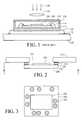
- FIG. 1is a depiction of a known optical sensor package arrangement.
- the optical sensor 104is formed on a first substrate 106 .
- the optical sensorreceives light 108 and generates electrical signals in proportion to the intensity of the received light and then transmits the electrical signals to conductors within the first substrate.
- the first substrateis typically an integrated circuit that has electrical interconnections between each pixel in the optical sensor and contact pads 110 that are formed on the surface of the first substrate. The contact pads on the surface of the first substrate allow electrical connections to be made to a larger scale package.
- the first substrate 106is physically attached to a second substrate 112 such as an injection molded plastic, a glass reinforced laminate, or a ceramic package.
- the contact pads on the first substrateare electrically connected to bonding pads on the second substrate by very fine bonding wires 114 .
- the optical sensor 104 and the first substrate 106are typically covered with an optical glass cover 116 in order to seal the optical sensor within a package and protect the optical sensor from the outside environment.
- the sealed packageis then electrically connected to contact pads of a circuit board 118 by package leads 120 and solder bonds 122 .
- the circuit boardconnects the optical sensor to other systems, such as memory and processors that are needed to support the desired functionality.
- a lens 130may also be located above the glass cover and the optical sensor in order to focus incoming light 108 onto the optical sensor.
- optical sensor packaging techniqueswork well, as the size of electronic devices, especially hand held devices, shrinks, there is a need to package the optical sensors in smaller packages.
- the need for smaller packagingis especially important in the height dimension of the package, as measured from the lens to the circuit board. That is, it is desirable to provide optical sensors in“thinner” packages.
- BGAball grid array
- an integrated circuitis connected to a BGA package and the BGA package is physically and electrically connected to a circuit board with solder balls.
- the solder ballsare soldered to contact pads on the BGA package and to corresponding contact pads on the circuit board.
- the solder ballsare placed in a closely spaced array.
- a solder reflow processis typically utilized to connect the solder balls to the conductive contact pads of the BGA package and to the conductive contact pads of the circuit board.
- the BGA mounting techniqueworks well, the BGA mounting technique is generally utilized for packaging and mounting non-light sensitive integrated circuits, such as microprocessors and application specific integrated circuits.
- An optical device packaging techniqueinvolves an optical sensor that is formed on a first substrate and flip chip bonded to a second substrate.
- the second substrateincludes a through hole or a transparent material that is aligned with the optical sensor in order to allow light to contact the optical sensor.
- the optical sensoris provided in a thin package that is useful in many applications, such as hand held cameras.
- a first embodiment of an optical device structureincludes an optical sensor, a first substrate, a second substrate, and a circuit board.
- the optical sensoris formed on or within the first substrate and the individual sensors or pixels of the optical sensor are electrically connected to contact pads that are exposed on the top surface of the first substrate.
- the first substrateis connected to the second substrate by solder balls that connect contact pads on the bottom surface of the second substrate to corresponding contact pads on the first substrate.
- the second substrateis a package substrate, such as an injection molded plastic substrate, a ceramic substrate, or a glass reinforced laminate.
- the second substrateincludes electrical conductors that electrically connect the first set of contact pads to a second set of contact pads on the periphery of the second substrate.
- the second substrateincludes a through hole that allows light to contact the optical sensor.
- the second substrateis connected to the circuit board with interconnects, such as solder balls, as is known in the art of ball grid array mounting.
- the interconnectsprovide an electrical connection between a second set of contact pads on the second substrate and corresponding contact pads on the circuit board.
- the first embodimentmay include an optical glass cover that is placed over the opening in the second substrate in order to protect the optical sensor from damage while allowing light to contact the optical sensor.
- the first embodimentmay include an optical grade structural adhesive that is applied directly over the optical sensor instead of an optical glass cover that is attached to the second substrate.
- the first embodimentmay include an optical lens system that is placed over the opening in the second substrate in order to enable focusing of light onto the optical sensor.
- the first embodimentmay include an optical glass substrate as the second substrate.
- the optical glass substratemay include metal patterning on the bottom surface that provides a portion of the electrical connection between the optical sensor and the circuit board.
- the first embodimentmay include an optically transparent glass structure that includes an integrated lens element, or multiple elements, as the second substrate.
- the first embodimentmay be incorporated into a camera housing that includes an opening for allowing light to contact the optical sensor.
- a second embodiment of an optical device structureincludes an optical sensor, a first substrate, and a circuit board as the second substrate.
- contact pads of the first substrateare connected to contact pads of the circuit board with conductive balls.
- the connection between the first substrate and the circuit boardprovides the electrical connection between the optical sensor and the circuit board.
- the circuit boardincludes a through hole that allows light to contact the optical sensor.
- a transparent circuit boardmay alternatively allow light to contact the optical sensor.
- the second embodimentmay include an optical glass cover that is placed over the opening in the circuit board in order to protect the optical sensor from damage while allowing light to contact the optical sensor.
- the second embodimentmay include an optical grade structural adhesive that is applied directly over the optical sensor instead of an optical glass cover that is attached to the circuit board.
- the second embodimentmay include an optical lens system that is placed over the opening in the circuit board in order to enable focusing of light onto the optical sensor.
- the second embodimentmay include a monolithic glass structure that includes a lens element or multiple lens elements as the circuit board.
- the monolithic glass structureforms part of a camera housing.
- FIG. 1is a depiction of a known optical sensor package arrangement in which an optical sensor package is wire bonded to a circuit board.
- FIG. 2is a cross sectional view of an optical device structure including an optical sensor that is formed on a first substrate and flip chip bonded to a second substrate, in accordance with an embodiment of the invention.
- FIG. 3is a top view of the first substrate shown in FIG. 2 taken at section 3 — 3 .
- FIG. 4Ais a cross sectional view of an optical device structure that includes an optical sensor, a first substrate, a second substrate, a circuit board, and an optical glass cover, in accordance with an embodiment of the invention.
- FIG. 4Bis a cross sectional view of an optical device structure that includes an optical sensor, a first substrate, a second substrate, a circuit board above the second substrate, and an optical glass cover, in accordance with an embodiment of the invention.
- FIG. 5is a cross sectional view of an optical device structure that is similar to FIG. 4A except that the optical glass cover is replaced with an optical grade structural adhesive, in accordance with an embodiment of the invention.
- FIG. 6is a cross sectional view of an optical device structure that is similar to FIG. 4A except that the optical glass cover is replaced with a lens system, in accordance with an embodiment of the invention.
- FIG. 7is a cross sectional view of an optical device structure that is similar to FIG. 4A except that the second substrate is a metal patterned glass, in accordance with an embodiment of the invention.
- FIG. 8is a cross sectional view of an optical device structure that is similar to FIG. 7 except that the metal patterned glass includes an integrated front lens element, in accordance with an embodiment of the invention.
- FIG. 9is a cross sectional view of a hand held camera that incorporates the optical device structure of FIG. 8, in accordance with an embodiment of the invention.
- FIG. 10Ais a cross sectional view of a hand held camera in which metal patterned glass serves as a circuit board, a package substrate, and a portion of the housing of a hand held camera, in accordance with an embodiment of the invention.
- FIG. 10Bis a cross sectional view of a hand held camera in which metal patterned glass with an integrated lens element serves as a circuit board, a package substrate, and a portion of the housing of a hand held camera, in accordance with an embodiment of the invention.
- FIG. 11is a cross sectional view of an optical device structure that includes an optical sensor, a first substrate, a circuit board, and an optical glass cover, in accordance with an embodiment of the invention.
- FIG. 12is a cross sectional view of an optical device structure that is similar to FIG. 11 except that the optical glass cover is replaced with an optical grade structural adhesive, in accordance with an embodiment of the invention.
- FIG. 13Ais a cross sectional view of an optical device structure that is similar to FIG. 11 except that the optical glass cover is replaced with a lens system, in accordance with an embodiment of the invention.
- FIG. 13Bis a cross sectional view of an optical device structure that is similar to FIG. 11 except that the circuit board is a transparent material, in accordance with an embodiment of the invention.
- FIG. 2is a cross sectional view of an optical device structure including an optical sensor that is flip chip bonded to a substrate.
- the cross sectional viewincludes an optical sensor 204 , a first substrate 206 , and a second substrate 212 .
- the optical sensoris formed on or within the first substrate and the individual sensors or pixels of the optical sensor are electrically connected to contact pads 210 that are exposed on the top surface of the first substrate.
- the optical sensoris a CCD array or an active pixel sensor array and the first substrate is an integrated circuit formed in a bulk silicon substrate.
- the first substrateincludes circuitry that is connected to each element of the optical sensor and to the contact pads that are exposed around the outer edge of the top surface of the first substrate.
- the first substrate 206is connected to the second substrate 212 at contact pads 214 that are exposed on the bottom surface of the second substrate.
- the second substratemay be a package substrate, such as ceramic or molded plastic or the second substrate may be a circuit board.
- the second substrateincludes a through hole 224 that allows light to contact the optical sensor.
- FIG. 2 and subsequent figures depict a through hole for allowing light to contact the optical sensorin other configurations, the second substrate may include a transparent material that allows light to contact the optical sensor or the second substrate may be a transparent material that allows light to contact the optical sensor.
- the contact pads 214 of the second substrateare electrically connected to the contact pads 210 of the first substrate 206 .
- the first substrate and second substrateare electrically connected with solder balls 226 , although the two substrates may be electrically connected utilizing other conductive members or materials, such as a conductive adhesive that electrically connects the contact pads of the two substrates.
- the contact pads of the two substratesmay be connected by a combination of conductive balls and an adhesive.
- the location of the contact pads on the first substrate and the second substratedetermines the alignment of the first substrate, and ultimately the optical sensor 204 , in relation to the second substrate and the opening 224 in the second substrate, as shown in FIG. 2 .
- FIG. 3is a top view of the first substrate 306 taken at section 3 — 3 .
- the top view of FIG. 3shows the first substrate in relation to the optical sensor 304 and in relation to the connection points 326 that electrically connect the first substrate to the second substrate. Although only ten connection points are shown for description purposes, an optical sensor typically has multiple connection points.
- FIG. 4Ais a cross sectional view of an optical device structure that incorporates the elements of FIG. 2 and 3.
- the optical device structure shown in FIG. 4Aincludes an optical sensor 404 , a first substrate 406 , a second substrate 412 , a circuit board 430 , and an optical glass cover 416 .
- the second substrateis a package substrate, such as an injection molded plastic substrate, a ceramic substrate, or a glass reinforced laminate.
- the second substrateincludes electrical conductors (not shown) that electrically connect the inner contact pads 414 to contact pads 432 on the periphery of the second substrate.
- the optical sensor 404 , the first substrate 406 and the connection between the first substrate and the second substrate 412are similar to those described with reference to FIGS. 2 and 3.
- the connection between the first substrate and the second substratemay include a structural adhesive 434 around the solder balls 426 and contact pads 410 and 414 , however this may not be required.
- the second substrate 412is connected to the circuit board 430 with interconnects 436 , such as solder balls, as is known in the art of ball grid array mounting.
- the interconnectsprovide an electrical connection between contact pads 432 on the second substrate and contact pads 438 on the circuit board.
- the contact pads 432could be located on either side of the second substrate.
- contact pads on the second substrate 412 and on the circuit board 430are connected to conductive leads (not shown) that enable electrical signals to travel through the second substrate and the circuit board, respectively.
- the individual light sensitive devices of the optical sensor 404are electrically connected to the conductive contact pads of the circuit board. Electrical signals generated by the optical sensor can be transmitted from the optical sensor and through the circuit board to other devices on the circuit board, such as memory and processors.
- the optical glass cover 416is placed over the through hole 424 in the second substrate 412 in order to protect the optical sensor 404 from damage while allowing light to contact the optical sensor.
- the optical glass coveris preferably attached to the top surface of the second substrate with an adhesive 440 in order to completely cover the through hose and to create a sealed environment for the optical sensor.
- the optical glass covermay not completely cover the through hole but covers substantially all of the through hole.
- the first substrate 406may also be attached to the circuit board 430 with an adhesive 442 , as shown in FIG. 4 A.
- the adhesivemay be thermally conductive in order to dissipate heat from the optical sensor 404 and the adhesive may provide a structurally secure connection between the optical sensor and the circuit board.
- a lens(not shown) may be located above the optical glass in order to focus light onto the optical sensor.
- FIG. 4 BAn embodiment of an optical device structure having the circuit board on the opposite side of the second substrate is shown in FIG. 4 B.
- the circuit boardhas an opening or a transparent section that allows light to contact the optical sensor 404 .
- the openingis large enough to allow the optical glass cover to pass through the opening.
- the circuit board location in FIG. 4Bcan be utilized in the embodiments of FIGS. 5, 6 , 7 , and 8 .
- FIG. 5is a cross sectional view of an optical device structure that is similar to FIG. 4 A.
- the optical device structure of FIG. 5includes an optical grade structural adhesive 544 that is applied directly over the optical sensor 504 instead of an optical glass cover that is attached to the second substrate 512 .
- the optical grade structural adhesiveis in direct contact with the optical sensor and the first and second substrates 506 and 512 .
- the optical grade structural adhesiveprotects the optical sensor from damage and may provide structural integrity to the connection between the first and second substrates.
- the first substrateis attached to the circuit board 530 with an adhesive 542 , although this is not critical to the invention.
- FIG. 6is a cross sectional view of an optical device structure that is similar to FIG. 4 A.
- the main difference between the optical device structure of FIG. 4 A and the optical device structure of FIG. 6is that the optical glass cover is replaced with an optical lens system 646 .
- the optical lens systemallows light to be focused onto the optical sensor 604 for applications such as hand held digital cameras.
- the lens 648 of the optical lens systemis adjustable to provide focusing at various distances and in other embodiments the lens may be fixed.
- the optical lens systemis attached to the top surface of the second substrate 612 in a manner that creates a clean environment for the optical sensor.
- the bottom surface of the first substrate 606is not attached to the circuit board 630 , although this is not critical.
- FIG. 7is a cross sectional view of an optical device structure that is similar to FIG. 4 A.
- the main difference between the optical device structure of FIG. 4 A and the optical device structure of FIG. 7is that the second substrate 712 in the optical device structure of FIG. 7 is an optical glass substrate.
- the optical glass substrateincludes metal patterning 750 on the bottom surface that provides a portion of the electrical connection between the optical sensor 704 and the circuit board 730 .
- the metal patterningcarries electrical signals from the first substrate 706 to the circuit board.
- the first substrate and the optical glass substrateare electrically connected by conductive balls 726 and physically connected by an adhesive 734 .
- the bottom surface of the optical glass substrate and the circuit boardare electrically connected by conductive balls 736 .
- the bottom surface of the first substrateis not attached to the circuit board, although this is desirable if better heat dissipation is required.
- optical glassis described, other transparent materials may be utilized for any of the described embodiments.
- FIG. 8is a cross sectional view of an optical device structure that is similar to FIG. 7 except that the second substrate 812 includes a front lens element 852 that is incorporated into the optical glass.
- the second substrateis an optically transparent monolithic glass structure that includes an integrated lens element that focuses light onto the optical sensor 804 .
- Other embodimentsmay include several lens elements.
- the optical glassincludes metal patterning 850 that conducts electrical signals from the first substrate to the circuit board.
- FIG. 9is a cross sectional view of a hand held camera that incorporates the optical device structure of FIG. 8 .
- the optical device structureis incorporated into a camera housing 954 that includes an opening 956 for allowing light to contact the optical sensor 904 .
- the circuit board 930may include at least one other component 958 , such as memory or a processor.
- FIG. 9represents one configuration for incorporating the optical device structure of FIG. 8 into a camera housing, it should be appreciated that other configurations are possible.
- FIG. 10Ais a cross sectional view of a hand held camera in which metal patterned glass 1012 serves as a circuit board and a package substrate.
- the metal patterned glassincludes conductive patterns 1050 that enable electrical signals to be transmitted from the optical sensor 1004 to other electronic components 1058 within the camera such as memory and/or a processor.
- the metal patterned glassalso forms a portion of the camera housing.
- the metal patterned glassis connected to a back camera housing 1054 that may be made of, for example, molded plastic or lightweight metal.
- FIG. 10Bshows that the metal patterned glass also includes an integrated lens 1052 that is incorporated into the optically transparent and monolithic element.
- Other embodimentsmay include several lens elements.
- FIG. 11is a cross sectional view of an optical device structure that incorporates the elements of FIGS. 2 and 3.
- the optical device structure shown in FIG. 11includes an optical sensor 1104 , a first substrate 1106 , a circuit board 1112 as the second substrate, and an optical glass cover 1116 .
- contact pads 1110 of the first substrateare connected to contact pads 1114 of the circuit board with conductive balls 1126 and an adhesive 1134 .
- a conductive adhesiveis utilized to connect the first substrate to the circuit board, it may not be required.
- Other techniques, such as solderingmay be utilized to connect the contact pads of the first substrate to the contact pads of the circuit board.
- the connection between the first substrate and the circuit boardprovides the electrical connection between the optical sensor and the circuit board.
- the circuit boardincludes a through hole 1124 that allows light to contact the optical sensor.
- a transparent circuit boardmay alternatively allow light to contact the optical sensor.
- conductive ballsare described, other conductive members may be utilized to form the electrical connection between the first substrate and the circuit board.
- the optical glass cover 1116is placed over the through hole 1124 in the circuit board in order to protect the optical sensor 1104 from damage while allowing light to contact the optical sensor.
- the optical glass coveris preferably attached to the top surface of the circuit board 1112 in a manner that creates a sealed environment for the optical sensor.
- FIG. 12is a cross sectional view of an optical device structure that is similar to FIG. 11 .
- the main difference between the optical device structure of FIG. 11 and the optical device structure of FIG. 12is that the optical device structure of FIG. 12 includes an optical grade structural adhesive 1244 that is applied directly over the optical sensor 1204 instead of an optical glass cover that is attached to the circuit board 1212 .
- the optical grade structural adhesiveis in direct contact with the optical sensor and the first substrate 1206 , and the circuit board.
- the optical grade structural adhesiveprotects the optical sensor from damage and may provide structural integrity to the connection between the first substrate and the circuit board.
- FIG. 13Ais a cross sectional view of an optical device structure that is similar to FIG. 11 .
- the main difference between the optical device structure of FIG. 11 and the optical device structure of FIG. 13Ais that the optical glass cover connected to the circuit board is replaced with an optical lens system 1346 that is connected to the circuit board 1312 .
- the optical lens systemallows light to be focused onto the optical sensor 1304 for applications such as hand held digital cameras.
- the lens 1348is adjustable to provide focusing at various distances and in other embodiments the lens may be fixed.
- the optical lens systemis attached to the top surface of the circuit board with an adhesive in order to create a sealed environment for the optical sensor.
- FIG. 13Bis cross sectional view of an optical device structure that is similar to FIG. 11 .
- the main differenceis that the circuit board itself is a transparent material, eliminating the need for an opening to pass light.
Landscapes
- Solid State Image Pick-Up Elements (AREA)
- Transforming Light Signals Into Electric Signals (AREA)
Abstract
Description
Claims (21)
Priority Applications (1)
| Application Number | Priority Date | Filing Date | Title |
|---|---|---|---|
| US09/513,797US6396116B1 (en) | 2000-02-25 | 2000-02-25 | Integrated circuit packaging for optical sensor devices |
Applications Claiming Priority (1)
| Application Number | Priority Date | Filing Date | Title |
|---|---|---|---|
| US09/513,797US6396116B1 (en) | 2000-02-25 | 2000-02-25 | Integrated circuit packaging for optical sensor devices |
Publications (1)
| Publication Number | Publication Date |
|---|---|
| US6396116B1true US6396116B1 (en) | 2002-05-28 |
Family
ID=24044705
Family Applications (1)
| Application Number | Title | Priority Date | Filing Date |
|---|---|---|---|
| US09/513,797Expired - LifetimeUS6396116B1 (en) | 2000-02-25 | 2000-02-25 | Integrated circuit packaging for optical sensor devices |
Country Status (1)
| Country | Link |
|---|---|
| US (1) | US6396116B1 (en) |
Cited By (115)
| Publication number | Priority date | Publication date | Assignee | Title |
|---|---|---|---|---|
| US20030016849A1 (en)* | 2001-04-27 | 2003-01-23 | Andrade Thomas L. | Capacitive sensor system with improved capacitance measuring sensitivity |
| US20030020495A1 (en)* | 2001-05-22 | 2003-01-30 | Andrade Thomas L. | Surface capacitance sensor system using buried stimulus electrode |
| US6552419B2 (en)* | 2001-01-25 | 2003-04-22 | Sharp Kabushiki Kaisha | Semiconductor device and liquid crystal module using the same |
| US6586824B1 (en)* | 2001-07-26 | 2003-07-01 | Amkor Technology, Inc. | Reduced thickness packaged electronic device |
| US6621616B1 (en)* | 1998-08-21 | 2003-09-16 | Gentex Corporation | Devices incorporating electrochromic elements and optical sensors |
| WO2002095801A3 (en)* | 2001-05-22 | 2003-10-30 | Control Security Inc I | Improved connection assembly for integrated circuit sensors |
| US20030205826A1 (en)* | 2000-05-19 | 2003-11-06 | Megic Corporation | Multiple chips bonded to packaging structure with low noise and multiple selectable functions |
| US20030209787A1 (en)* | 2002-05-07 | 2003-11-13 | Masayuki Kondo | Package for mounting a solid state image sensor |
| US20030220574A1 (en)* | 2002-03-18 | 2003-11-27 | Sarcos Investments Lc. | Miniaturized imaging device including utility aperture and SSID |
| US20030223008A1 (en)* | 2002-05-28 | 2003-12-04 | Samsung Electro-Mechanics Co., Ltd. | Image sensor module and process of fabricating the same |
| US20030222325A1 (en)* | 2002-03-18 | 2003-12-04 | Sarcos Investments Lc. | Miniaturized imaging device with integrated circuit connector system |
| US6680525B1 (en)* | 2003-01-09 | 2004-01-20 | Kingpak Technology Inc. | Stacked structure of an image sensor |
| US6683298B1 (en)* | 2000-11-20 | 2004-01-27 | Agilent Technologies Inc. | Image sensor packaging with package cavity sealed by the imaging optics |
| US6686653B2 (en)* | 2000-06-28 | 2004-02-03 | Institut National D'optique | Miniature microdevice package and process for making thereof |
| US6686588B1 (en)* | 2001-01-16 | 2004-02-03 | Amkor Technology, Inc. | Optical module with lens integral holder |
| US20040023437A1 (en)* | 2001-11-29 | 2004-02-05 | Jong-Tae Moon | Method for optical module packaging of flip chip bonding |
| US6703713B1 (en)* | 2002-09-10 | 2004-03-09 | Siliconware Precision Industries Co., Ltd. | Window-type multi-chip semiconductor package |
| US6707125B2 (en)* | 2001-11-22 | 2004-03-16 | Matsushita Electric Industrial Co., Ltd. | Solid-state imaging apparatus and manufacturing method thereof |
| US6707141B2 (en)* | 1996-06-26 | 2004-03-16 | Micron Technology, Inc. | Multi-chip module substrate for use with leads-over chip type semiconductor devices |
| US6707148B1 (en)* | 2002-05-21 | 2004-03-16 | National Semiconductor Corporation | Bumped integrated circuits for optical applications |
| US6713876B1 (en)* | 1999-11-04 | 2004-03-30 | Stmicroelectronics S.A. | Optical semiconductor housing and method for making same |
| US20040081473A1 (en)* | 2002-10-25 | 2004-04-29 | Imran Sherazi | Direct attach optical receiver module and method of testing |
| US6740950B2 (en)* | 2001-01-15 | 2004-05-25 | Amkor Technology, Inc. | Optical device packages having improved conductor efficiency, optical coupling and thermal transfer |
| US6740973B1 (en)* | 2003-01-09 | 2004-05-25 | Kingpak Technology Inc. | Stacked structure for an image sensor |
| US20040114851A1 (en)* | 2002-12-12 | 2004-06-17 | Tecktiong Tan | Optical information processing circuit assembly |
| US20040124486A1 (en)* | 2002-12-26 | 2004-07-01 | Katsumi Yamamoto | Image sensor adapted for reduced component chip scale packaging |
| US6759744B2 (en)* | 2001-10-11 | 2004-07-06 | Alps Electric Co., Ltd. | Electronic circuit unit suitable for miniaturization |
| US20040153695A1 (en)* | 2002-12-11 | 2004-08-05 | Sun Microsystems, Inc. | System and method for interconnecting nodes of a redundant computer system |
| US6774481B2 (en)* | 2000-08-28 | 2004-08-10 | Canon Kabushiki Kaisha | Solid-state image pickup device |
| FR2851374A1 (en)* | 2003-02-18 | 2004-08-20 | St Microelectronics Sa | SEMICONDUCTOR PACKAGE WITH INTEGRATED CIRCUIT CHIP CARRIED BY ELECTRICAL CONNECTION LEGS |
| US20040195492A1 (en)* | 2003-04-07 | 2004-10-07 | Hsin Chung Hsien | Image sensor having a photosensitive chip mounted to a metal sheet |
| JP2004287215A (en)* | 2003-03-24 | 2004-10-14 | Fuji Photo Film Co Ltd | Transmission type optical modulation apparatus and method for packaging the same |
| US20040217454A1 (en)* | 2001-05-18 | 2004-11-04 | Remi Brechignac | Optical semiconductor package with incorporated lens and shielding |
| US20040217363A1 (en)* | 2002-04-18 | 2004-11-04 | Matsushita Electric Industrial Co., Ltd. | Integrated circuit device packaging structure and packaging method |
| US20040222510A1 (en)* | 2003-03-24 | 2004-11-11 | Akiyoshi Aoyagi | Semiconductor device, semiconductor pack age, electronic device, electronic apparatus, and manufacturing methods of semiconductor device and electronic device |
| US6844619B2 (en)* | 2000-12-01 | 2005-01-18 | Nec Corporation | Compact semiconductor device capable of mounting a plurality of semiconductor chips with high density and method of manufacturing the same |
| US20050013544A1 (en)* | 1999-08-27 | 2005-01-20 | Canon Kabushiki Kaisha | Surface optical device apparatus, method of fabricating the same, and apparatus using the same |
| US20050073605A1 (en)* | 2003-10-06 | 2005-04-07 | Burns Jeffrey H. | Integrated optical filter |
| US20050077451A1 (en)* | 2003-10-10 | 2005-04-14 | Matsushita Electric Industrial Co., Ltd. | Optical device and production method thereof |
| US20050082490A1 (en)* | 2000-12-29 | 2005-04-21 | Perillat Patrick D. | Optical semiconductor housing with transparent chip and method for making same |
| US20050110131A1 (en)* | 2003-11-24 | 2005-05-26 | Lee Kevin J. | Vertical wafer stacking using an interposer |
| US20050205898A1 (en)* | 2002-05-30 | 2005-09-22 | Koninkijkle Phillips Electronics N.V. | Electronic imaging device |
| US20050236708A1 (en)* | 2004-04-27 | 2005-10-27 | Farnworth Warren M | Microelectronic imaging devices and methods of packaging microelectronic imaging devices |
| US20050279916A1 (en)* | 2004-05-03 | 2005-12-22 | Tessera, Inc. | Image sensor package and fabrication method |
| US6984866B1 (en)* | 2003-03-17 | 2006-01-10 | National Semiconductor Corporation | Flip chip optical semiconductor on a PCB |
| US20060016973A1 (en)* | 2004-07-21 | 2006-01-26 | Advanced Semiconductor Engineering, Inc. | Multi-chip image sensor package module |
| US20060024857A1 (en)* | 2004-07-28 | 2006-02-02 | Industrial Technology Research Institute | Image sensor package structure and method for fabricating the same |
| US20060027905A1 (en)* | 2003-02-05 | 2006-02-09 | Michael Bauer | Biosensor with smart card configuration |
| US20060049338A1 (en)* | 2002-10-25 | 2006-03-09 | Imran Sherazi | Direct attach optical receiver module and method of testing |
| US20060060765A1 (en)* | 2004-09-21 | 2006-03-23 | Tai-Yuan Huang | Photosensitive bonding package structure |
| US20060061889A1 (en)* | 2004-09-21 | 2006-03-23 | Delphi Technologies, Inc. | Electronic module with light-blocking features |
| US7059040B1 (en)* | 2001-01-16 | 2006-06-13 | Amkor Technology, Inc. | Optical module with lens integral holder fabrication method |
| US20060146172A1 (en)* | 2002-03-18 | 2006-07-06 | Jacobsen Stephen C | Miniaturized utility device having integrated optical capabilities |
| US20060223229A1 (en)* | 2002-07-19 | 2006-10-05 | Asat Ltd. | Ball grid array package and process for manufacturing same |
| US20060274297A1 (en)* | 2005-06-02 | 2006-12-07 | Canon Kabushiki Kaisha | Photo detector unit and exposure apparatus having the same |
| US7224056B2 (en)* | 2003-09-26 | 2007-05-29 | Tessera, Inc. | Back-face and edge interconnects for lidded package |
| US20070158833A1 (en)* | 2006-01-04 | 2007-07-12 | Soo-San Park | Integrated circuit package system including stacked die |
| US20070166867A1 (en)* | 2006-01-04 | 2007-07-19 | Chow Seng G | Integrated circuit package system with image sensor system |
| US7265440B2 (en) | 2003-06-16 | 2007-09-04 | Tessera Technologies Hungary Kft. | Methods and apparatus for packaging integrated circuit devices |
| US20080020511A1 (en)* | 2006-07-19 | 2008-01-24 | Advanced Chip Engineering Technology Inc. | Structure of image sensor module and a method for manufacturing of wafer level package |
| DE102006038302A1 (en)* | 2006-08-16 | 2008-02-21 | Atmel Germany Gmbh | Optical sensor unit for optical scanning device of data drive e.g. DVD drive, has laminar contacting unit provided with opening, which is formed adjacent to surrounding on photosensitive area of semiconductor component for light incidence |
| US20080050943A1 (en)* | 2006-08-25 | 2008-02-28 | Primax Electronics Ltd. | Camera module and assembling process thereof |
| US20080125349A1 (en)* | 2004-04-15 | 2008-05-29 | Alkermes, Inc. | Polymer-based sustained release device |
| KR100836658B1 (en) | 2005-10-11 | 2008-06-10 | 삼성전기주식회사 | Optical modulator module package and manufacturing method thereof |
| US20080149367A1 (en)* | 2006-12-22 | 2008-06-26 | Hon Hai Precision Industry Co., Ltd. | Printed circuit board and light sensing device using the same |
| US20080169549A1 (en)* | 2005-04-29 | 2008-07-17 | Flynn Carson | Stacked integrated circuit package system and method of manufacture therefor |
| US20080179729A1 (en)* | 2005-03-31 | 2008-07-31 | Il Kwon Shim | Encapsulant cavity integrated circuit package system |
| US20080191333A1 (en)* | 2007-02-08 | 2008-08-14 | Advanced Chip Engineering Technology Inc. | Image sensor package with die receiving opening and method of the same |
| KR100857172B1 (en) | 2005-10-11 | 2008-09-05 | 삼성전기주식회사 | Mems module package |
| CN100438023C (en)* | 2005-03-09 | 2008-11-26 | 松下电器产业株式会社 | Imaging module and method for forming the same |
| US20080304143A1 (en)* | 2007-06-05 | 2008-12-11 | Jacobsen Stephen C | Mini-scope for multi-directional imaging |
| US20090009611A1 (en)* | 2007-07-06 | 2009-01-08 | Kye Systems Corp. | Thin-type image capturing module structure for a web cam |
| US7479398B2 (en) | 2003-07-03 | 2009-01-20 | Tessera Technologies Hungary Kft. | Methods and apparatus for packaging integrated circuit devices |
| US20090026567A1 (en)* | 2004-07-28 | 2009-01-29 | Industrial Technology Research Institute | Image sensor package structure and method for fabricating the same |
| US7539366B1 (en)* | 2008-01-04 | 2009-05-26 | International Business Machines Corporation | Optical transceiver module |
| US20090180197A1 (en)* | 2008-01-11 | 2009-07-16 | Sterling Lc | Grin lens microscope system |
| US7566955B2 (en) | 2001-08-28 | 2009-07-28 | Tessera, Inc. | High-frequency chip packages |
| US20090224386A1 (en)* | 2008-03-07 | 2009-09-10 | Stats Chippac, Ltd. | Optical Semiconductor Device Having Pre-Molded Leadframe with Window and Method Therefor |
| US20090283887A1 (en)* | 2008-05-16 | 2009-11-19 | Panasonic Corporation | Optical semiconductor device |
| US20090302464A1 (en)* | 2006-12-04 | 2009-12-10 | Tomokatsu Nakagawa | Semiconductor device |
| US20100102458A1 (en)* | 2008-10-28 | 2010-04-29 | Seng Guan Chow | Semiconductor package system with cavity substrate and manufacturing method therefor |
| US7750482B2 (en) | 2006-02-09 | 2010-07-06 | Stats Chippac Ltd. | Integrated circuit package system including zero fillet resin |
| US7781852B1 (en)* | 2006-12-05 | 2010-08-24 | Amkor Technology, Inc. | Membrane die attach circuit element package and method therefor |
| US20100289131A1 (en)* | 2009-05-18 | 2010-11-18 | Stats Chippac, Ltd. | Semiconductor Device and Method of Forming Overlapping Semiconductor Die with Coplanar Vertical Interconnect Structure |
| US20110064363A1 (en)* | 2009-09-14 | 2011-03-17 | Zarlink Semiconductor Ab | Self-aligned carrier assembly for optical device supporting wafer scale methods |
| US20110084118A1 (en)* | 2009-10-13 | 2011-04-14 | Renesas Technology Corp. | Manufacturing method of solid-state image pickup device |
| US7936062B2 (en) | 2006-01-23 | 2011-05-03 | Tessera Technologies Ireland Limited | Wafer level chip packaging |
| US20120002915A1 (en)* | 2010-07-05 | 2012-01-05 | Fujitsu Limited | Optical module and fabrication method |
| US8143095B2 (en) | 2005-03-22 | 2012-03-27 | Tessera, Inc. | Sequential fabrication of vertical conductive interconnects in capped chips |
| US20120099872A1 (en)* | 2009-06-16 | 2012-04-26 | Autonetworks Technologies, Ltd. | Optical communication module |
| US20120248553A1 (en)* | 2009-11-19 | 2012-10-04 | Dai Nippon Printing Co., Ltd. | Sensor device and manufacturing method thereof |
| WO2013028616A3 (en)* | 2011-08-19 | 2013-06-27 | Imi Usa, Inc. | Flip-chip bonded imager die |
| US8486735B2 (en) | 2008-07-30 | 2013-07-16 | Raytheon Company | Method and device for incremental wavelength variation to analyze tissue |
| US20130285185A1 (en)* | 2012-04-25 | 2013-10-31 | Samsung Electronics Co., Ltd. | Image sensor package |
| US20130292786A1 (en)* | 2012-05-02 | 2013-11-07 | Analog Devices, Inc. | Integrated optical sensor module |
| US8604605B2 (en) | 2007-01-05 | 2013-12-10 | Invensas Corp. | Microelectronic assembly with multi-layer support structure |
| US8614768B2 (en) | 2002-03-18 | 2013-12-24 | Raytheon Company | Miniaturized imaging device including GRIN lens optically coupled to SSID |
| US20140047711A1 (en)* | 2006-04-11 | 2014-02-20 | Flextronics Ap Llc | Method for mounting protective covers over image capture devices and devices manufactured thereby |
| US8690762B2 (en) | 2008-06-18 | 2014-04-08 | Raytheon Company | Transparent endoscope head defining a focal length |
| US8704349B2 (en) | 2006-02-14 | 2014-04-22 | Stats Chippac Ltd. | Integrated circuit package system with exposed interconnects |
| US8717428B2 (en) | 2009-10-01 | 2014-05-06 | Raytheon Company | Light diffusion apparatus |
| US8828028B2 (en) | 2009-11-03 | 2014-09-09 | Raytheon Company | Suture device and method for closing a planar opening |
| CN104716115A (en)* | 2013-12-12 | 2015-06-17 | 恩智浦有限公司 | Sensor package and manufacturing method thereof |
| US9060704B2 (en) | 2008-11-04 | 2015-06-23 | Sarcos Lc | Method and device for wavelength shifted imaging |
| US9144664B2 (en) | 2009-10-01 | 2015-09-29 | Sarcos Lc | Method and apparatus for manipulating movement of a micro-catheter |
| US9590129B2 (en) | 2014-11-19 | 2017-03-07 | Analog Devices Global | Optical sensor module |
| US9661996B2 (en) | 2009-10-01 | 2017-05-30 | Sarcos Lc | Needle delivered imaging device |
| CN109791267A (en)* | 2016-09-28 | 2019-05-21 | 夏普株式会社 | Optical device and camera model |
| US10712197B2 (en) | 2018-01-11 | 2020-07-14 | Analog Devices Global Unlimited Company | Optical sensor package |
| US10884551B2 (en) | 2013-05-16 | 2021-01-05 | Analog Devices, Inc. | Integrated gesture sensor module |
| CN112652611A (en)* | 2020-12-18 | 2021-04-13 | 维沃移动通信有限公司 | Sensor packaging structure and electronic equipment |
| DE102022208782A1 (en)* | 2022-07-19 | 2024-01-25 | Continental Autonomous Mobility Germany GmbH | Camera module and method for producing a camera module |
| WO2024017443A1 (en)* | 2022-07-19 | 2024-01-25 | Continental Autonomous Mobility Germany GmbH | Camera module and method for producing a camera module |
| US20240168245A1 (en)* | 2022-11-18 | 2024-05-23 | Stmicroelectronics (Grenoble 2) Sas | Integrated circuit comprising an assembly of an electronic chip, an optical element and a substrate and corresponding manufacturing method |
| US12389545B2 (en)* | 2022-02-09 | 2025-08-12 | Samsung Electronics Co., Ltd. | Semiconductor packages having circuit boards |
Citations (10)
| Publication number | Priority date | Publication date | Assignee | Title |
|---|---|---|---|---|
| US5394490A (en) | 1992-08-11 | 1995-02-28 | Hitachi, Ltd. | Semiconductor device having an optical waveguide interposed in the space between electrode members |
| US5811799A (en) | 1997-07-31 | 1998-09-22 | Wu; Liang-Chung | Image sensor package having a wall with a sealed cover |
| US5821532A (en) | 1997-06-16 | 1998-10-13 | Eastman Kodak Company | Imager package substrate |
| US5861654A (en) | 1995-11-28 | 1999-01-19 | Eastman Kodak Company | Image sensor assembly |
| US6011294A (en)* | 1996-04-08 | 2000-01-04 | Eastman Kodak Company | Low cost CCD packaging |
| US6059188A (en)* | 1993-10-25 | 2000-05-09 | Symbol Technologies | Packaged mirror including mirror travel stops |
| US6130448A (en)* | 1998-08-21 | 2000-10-10 | Gentex Corporation | Optical sensor package and method of making same |
| US6147389A (en)* | 1999-06-04 | 2000-11-14 | Silicon Film Technologies, Inc. | Image sensor package with image plane reference |
| US6150724A (en)* | 1998-03-02 | 2000-11-21 | Motorola, Inc. | Multi-chip semiconductor device and method for making the device by using multiple flip chip interfaces |
| US6303387B1 (en)* | 1997-06-17 | 2001-10-16 | Corning Incorporated | Method of transferring a liquid drop from a multiwell plate and/or chemical assay |
- 2000
- 2000-02-25USUS09/513,797patent/US6396116B1/ennot_activeExpired - Lifetime
Patent Citations (10)
| Publication number | Priority date | Publication date | Assignee | Title |
|---|---|---|---|---|
| US5394490A (en) | 1992-08-11 | 1995-02-28 | Hitachi, Ltd. | Semiconductor device having an optical waveguide interposed in the space between electrode members |
| US6059188A (en)* | 1993-10-25 | 2000-05-09 | Symbol Technologies | Packaged mirror including mirror travel stops |
| US5861654A (en) | 1995-11-28 | 1999-01-19 | Eastman Kodak Company | Image sensor assembly |
| US6011294A (en)* | 1996-04-08 | 2000-01-04 | Eastman Kodak Company | Low cost CCD packaging |
| US5821532A (en) | 1997-06-16 | 1998-10-13 | Eastman Kodak Company | Imager package substrate |
| US6303387B1 (en)* | 1997-06-17 | 2001-10-16 | Corning Incorporated | Method of transferring a liquid drop from a multiwell plate and/or chemical assay |
| US5811799A (en) | 1997-07-31 | 1998-09-22 | Wu; Liang-Chung | Image sensor package having a wall with a sealed cover |
| US6150724A (en)* | 1998-03-02 | 2000-11-21 | Motorola, Inc. | Multi-chip semiconductor device and method for making the device by using multiple flip chip interfaces |
| US6130448A (en)* | 1998-08-21 | 2000-10-10 | Gentex Corporation | Optical sensor package and method of making same |
| US6147389A (en)* | 1999-06-04 | 2000-11-14 | Silicon Film Technologies, Inc. | Image sensor package with image plane reference |
Cited By (200)
| Publication number | Priority date | Publication date | Assignee | Title |
|---|---|---|---|---|
| US6707141B2 (en)* | 1996-06-26 | 2004-03-16 | Micron Technology, Inc. | Multi-chip module substrate for use with leads-over chip type semiconductor devices |
| US6621616B1 (en)* | 1998-08-21 | 2003-09-16 | Gentex Corporation | Devices incorporating electrochromic elements and optical sensors |
| US6970612B2 (en)* | 1999-08-27 | 2005-11-29 | Canon Kabushiki Kaisha | Surface optical device apparatus, method of fabricating the same, and apparatus using the same |
| US20050013544A1 (en)* | 1999-08-27 | 2005-01-20 | Canon Kabushiki Kaisha | Surface optical device apparatus, method of fabricating the same, and apparatus using the same |
| US6713876B1 (en)* | 1999-11-04 | 2004-03-30 | Stmicroelectronics S.A. | Optical semiconductor housing and method for making same |
| US20030205826A1 (en)* | 2000-05-19 | 2003-11-06 | Megic Corporation | Multiple chips bonded to packaging structure with low noise and multiple selectable functions |
| US8148806B2 (en) | 2000-05-19 | 2012-04-03 | Megica Corporation | Multiple chips bonded to packaging structure with low noise and multiple selectable functions |
| US7205646B2 (en)* | 2000-05-19 | 2007-04-17 | Megica Corporation | Electronic device and chip package |
| US6791192B2 (en)* | 2000-05-19 | 2004-09-14 | Megic Corporation | Multiple chips bonded to packaging structure with low noise and multiple selectable functions |
| US6686653B2 (en)* | 2000-06-28 | 2004-02-03 | Institut National D'optique | Miniature microdevice package and process for making thereof |
| US6774481B2 (en)* | 2000-08-28 | 2004-08-10 | Canon Kabushiki Kaisha | Solid-state image pickup device |
| US6683298B1 (en)* | 2000-11-20 | 2004-01-27 | Agilent Technologies Inc. | Image sensor packaging with package cavity sealed by the imaging optics |
| US6844619B2 (en)* | 2000-12-01 | 2005-01-18 | Nec Corporation | Compact semiconductor device capable of mounting a plurality of semiconductor chips with high density and method of manufacturing the same |
| US20050082657A1 (en)* | 2000-12-01 | 2005-04-21 | Nec Corporation | Compact semiconductor device capable of mounting a plurality of semiconductor chips with high density and method of manufacturing the same |
| US7218005B2 (en) | 2000-12-01 | 2007-05-15 | Nec Corporation | Compact semiconductor device capable of mounting a plurality of semiconductor chips with high density and method of manufacturing the same |
| US7214996B2 (en)* | 2000-12-29 | 2007-05-08 | Stmicroelectronics S.A. | Optical semiconductor housing with transparent chip and method for making same |
| US20050082490A1 (en)* | 2000-12-29 | 2005-04-21 | Perillat Patrick D. | Optical semiconductor housing with transparent chip and method for making same |
| US6740950B2 (en)* | 2001-01-15 | 2004-05-25 | Amkor Technology, Inc. | Optical device packages having improved conductor efficiency, optical coupling and thermal transfer |
| US6686588B1 (en)* | 2001-01-16 | 2004-02-03 | Amkor Technology, Inc. | Optical module with lens integral holder |
| US7059040B1 (en)* | 2001-01-16 | 2006-06-13 | Amkor Technology, Inc. | Optical module with lens integral holder fabrication method |
| US7609461B1 (en) | 2001-01-16 | 2009-10-27 | Amkor Technology, Inc. | Optical module having cavity substrate |
| US6552419B2 (en)* | 2001-01-25 | 2003-04-22 | Sharp Kabushiki Kaisha | Semiconductor device and liquid crystal module using the same |
| US20030016849A1 (en)* | 2001-04-27 | 2003-01-23 | Andrade Thomas L. | Capacitive sensor system with improved capacitance measuring sensitivity |
| US7256589B2 (en) | 2001-04-27 | 2007-08-14 | Atrua Technologies, Inc. | Capacitive sensor system with improved capacitance measuring sensitivity |
| US7327005B2 (en)* | 2001-05-18 | 2008-02-05 | Stmicroelectronics Sa | Optical semiconductor package with incorporated lens and shielding |
| US20040217454A1 (en)* | 2001-05-18 | 2004-11-04 | Remi Brechignac | Optical semiconductor package with incorporated lens and shielding |
| US7259573B2 (en) | 2001-05-22 | 2007-08-21 | Atrua Technologies, Inc. | Surface capacitance sensor system using buried stimulus electrode |
| WO2002095801A3 (en)* | 2001-05-22 | 2003-10-30 | Control Security Inc I | Improved connection assembly for integrated circuit sensors |
| US20030020495A1 (en)* | 2001-05-22 | 2003-01-30 | Andrade Thomas L. | Surface capacitance sensor system using buried stimulus electrode |
| US6586824B1 (en)* | 2001-07-26 | 2003-07-01 | Amkor Technology, Inc. | Reduced thickness packaged electronic device |
| US7566955B2 (en) | 2001-08-28 | 2009-07-28 | Tessera, Inc. | High-frequency chip packages |
| US6759744B2 (en)* | 2001-10-11 | 2004-07-06 | Alps Electric Co., Ltd. | Electronic circuit unit suitable for miniaturization |
| US6707125B2 (en)* | 2001-11-22 | 2004-03-16 | Matsushita Electric Industrial Co., Ltd. | Solid-state imaging apparatus and manufacturing method thereof |
| US6707161B2 (en)* | 2001-11-29 | 2004-03-16 | Electronics And Telecommunications Research Institute | Optical module package of flip chip bonding |
| US6825065B2 (en) | 2001-11-29 | 2004-11-30 | Electronics And Telecommunications Research Institute | Method for optical module packaging of flip chip bonding |
| US20040023437A1 (en)* | 2001-11-29 | 2004-02-05 | Jong-Tae Moon | Method for optical module packaging of flip chip bonding |
| US20030220574A1 (en)* | 2002-03-18 | 2003-11-27 | Sarcos Investments Lc. | Miniaturized imaging device including utility aperture and SSID |
| US7591780B2 (en)* | 2002-03-18 | 2009-09-22 | Sterling Lc | Miniaturized imaging device with integrated circuit connector system |
| US7787939B2 (en) | 2002-03-18 | 2010-08-31 | Sterling Lc | Miniaturized imaging device including utility aperture and SSID |
| US7629659B2 (en) | 2002-03-18 | 2009-12-08 | Sterling Lc | Miniaturized imaging device with integrated circuit connector system |
| US20060146172A1 (en)* | 2002-03-18 | 2006-07-06 | Jacobsen Stephen C | Miniaturized utility device having integrated optical capabilities |
| US20080185672A1 (en)* | 2002-03-18 | 2008-08-07 | Jacobsen Stephen C | Miniaturized imaging device with integrated circuit connector system |
| US20030222325A1 (en)* | 2002-03-18 | 2003-12-04 | Sarcos Investments Lc. | Miniaturized imaging device with integrated circuit connector system |
| US8614768B2 (en) | 2002-03-18 | 2013-12-24 | Raytheon Company | Miniaturized imaging device including GRIN lens optically coupled to SSID |
| US7663200B2 (en)* | 2002-04-18 | 2010-02-16 | Panasonic Corporation | Integrated circuit device packaging structure and packaging method |
| US20050151216A1 (en)* | 2002-04-18 | 2005-07-14 | Matsushita Electric Industrial Co., Ltd. | Integrated circuit device packaging structure and packaging method |
| US20040217363A1 (en)* | 2002-04-18 | 2004-11-04 | Matsushita Electric Industrial Co., Ltd. | Integrated circuit device packaging structure and packaging method |
| US6774447B2 (en)* | 2002-05-07 | 2004-08-10 | Mitsui Chemicals, Inc. | Package having an opening in a surface thereof for mounting a solid state image sensor |
| US20030209787A1 (en)* | 2002-05-07 | 2003-11-13 | Masayuki Kondo | Package for mounting a solid state image sensor |
| US7012282B1 (en)* | 2002-05-21 | 2006-03-14 | National Semiconductor Corporation | Bumped integrated circuits for optical applications |
| US6707148B1 (en)* | 2002-05-21 | 2004-03-16 | National Semiconductor Corporation | Bumped integrated circuits for optical applications |
| US20030223008A1 (en)* | 2002-05-28 | 2003-12-04 | Samsung Electro-Mechanics Co., Ltd. | Image sensor module and process of fabricating the same |
| US20050205898A1 (en)* | 2002-05-30 | 2005-09-22 | Koninkijkle Phillips Electronics N.V. | Electronic imaging device |
| US20060223229A1 (en)* | 2002-07-19 | 2006-10-05 | Asat Ltd. | Ball grid array package and process for manufacturing same |
| US6703713B1 (en)* | 2002-09-10 | 2004-03-09 | Siliconware Precision Industries Co., Ltd. | Window-type multi-chip semiconductor package |
| US7224910B2 (en) | 2002-10-25 | 2007-05-29 | Gennum Corporation | Direct attach optical receiver module and method of testing |
| US20060049338A1 (en)* | 2002-10-25 | 2006-03-09 | Imran Sherazi | Direct attach optical receiver module and method of testing |
| US7391005B2 (en) | 2002-10-25 | 2008-06-24 | Gennum Corporation | Direct attach optical receiver module and method of testing |
| US20040081473A1 (en)* | 2002-10-25 | 2004-04-29 | Imran Sherazi | Direct attach optical receiver module and method of testing |
| US20040153695A1 (en)* | 2002-12-11 | 2004-08-05 | Sun Microsystems, Inc. | System and method for interconnecting nodes of a redundant computer system |
| US20040114851A1 (en)* | 2002-12-12 | 2004-06-17 | Tecktiong Tan | Optical information processing circuit assembly |
| US7324715B2 (en)* | 2002-12-12 | 2008-01-29 | Delphi Technologies, Inc. | Optical information processing circuit assembly |
| US20040124486A1 (en)* | 2002-12-26 | 2004-07-01 | Katsumi Yamamoto | Image sensor adapted for reduced component chip scale packaging |
| CN100373628C (en)* | 2002-12-26 | 2008-03-05 | 华微半导体(上海)有限责任公司 | Image Sensor Adapted to Chip Scale Package with Reduced Components |
| US6740973B1 (en)* | 2003-01-09 | 2004-05-25 | Kingpak Technology Inc. | Stacked structure for an image sensor |
| US6680525B1 (en)* | 2003-01-09 | 2004-01-20 | Kingpak Technology Inc. | Stacked structure of an image sensor |
| US20060027905A1 (en)* | 2003-02-05 | 2006-02-09 | Michael Bauer | Biosensor with smart card configuration |
| US7566968B2 (en)* | 2003-02-05 | 2009-07-28 | Siemens Aktiengesellschaft | Biosensor with smart card configuration |
| US20050006732A1 (en)* | 2003-02-18 | 2005-01-13 | Stmicroelectronics Sa | Semiconductor package containing an integrated-circuit chip supported by electrical connection leads |
| FR2851374A1 (en)* | 2003-02-18 | 2004-08-20 | St Microelectronics Sa | SEMICONDUCTOR PACKAGE WITH INTEGRATED CIRCUIT CHIP CARRIED BY ELECTRICAL CONNECTION LEGS |
| US7030471B2 (en) | 2003-02-18 | 2006-04-18 | Stmicroelectronics S.A. | Semiconductor package containing an integrated-circuit chip supported by electrical connection leads |
| US6984866B1 (en)* | 2003-03-17 | 2006-01-10 | National Semiconductor Corporation | Flip chip optical semiconductor on a PCB |
| JP2004287215A (en)* | 2003-03-24 | 2004-10-14 | Fuji Photo Film Co Ltd | Transmission type optical modulation apparatus and method for packaging the same |
| US20040222510A1 (en)* | 2003-03-24 | 2004-11-11 | Akiyoshi Aoyagi | Semiconductor device, semiconductor pack age, electronic device, electronic apparatus, and manufacturing methods of semiconductor device and electronic device |
| US7091619B2 (en)* | 2003-03-24 | 2006-08-15 | Seiko Epson Corporation | Semiconductor device, semiconductor package, electronic device, electronic apparatus, and manufacturing methods of semiconductor device and electronic device |
| US6933493B2 (en)* | 2003-04-07 | 2005-08-23 | Kingpak Technology Inc. | Image sensor having a photosensitive chip mounted to a metal sheet |
| US20040195492A1 (en)* | 2003-04-07 | 2004-10-07 | Hsin Chung Hsien | Image sensor having a photosensitive chip mounted to a metal sheet |
| US7265440B2 (en) | 2003-06-16 | 2007-09-04 | Tessera Technologies Hungary Kft. | Methods and apparatus for packaging integrated circuit devices |
| US7642629B2 (en) | 2003-06-16 | 2010-01-05 | Tessera Technologies Hungary Kft. | Methods and apparatus for packaging integrated circuit devices |
| US7479398B2 (en) | 2003-07-03 | 2009-01-20 | Tessera Technologies Hungary Kft. | Methods and apparatus for packaging integrated circuit devices |
| US7495341B2 (en) | 2003-07-03 | 2009-02-24 | Tessera Technologies Hungary Kft. | Methods and apparatus for packaging integrated circuit devices |
| US7224056B2 (en)* | 2003-09-26 | 2007-05-29 | Tessera, Inc. | Back-face and edge interconnects for lidded package |
| US20050073605A1 (en)* | 2003-10-06 | 2005-04-07 | Burns Jeffrey H. | Integrated optical filter |
| US7485848B2 (en) | 2003-10-10 | 2009-02-03 | Panasonic Corporation | Optical device and production method thereof |
| US7755030B2 (en) | 2003-10-10 | 2010-07-13 | Panasonic Corporation | Optical device including a wiring having a reentrant cavity |
| US20050077451A1 (en)* | 2003-10-10 | 2005-04-14 | Matsushita Electric Industrial Co., Ltd. | Optical device and production method thereof |
| US20090032684A1 (en)* | 2003-10-10 | 2009-02-05 | Matsushita Electric Industrial Co., Ltd. | Optical device and production method thereof |
| US20050110131A1 (en)* | 2003-11-24 | 2005-05-26 | Lee Kevin J. | Vertical wafer stacking using an interposer |
| US20080125349A1 (en)* | 2004-04-15 | 2008-05-29 | Alkermes, Inc. | Polymer-based sustained release device |
| US20050236708A1 (en)* | 2004-04-27 | 2005-10-27 | Farnworth Warren M | Microelectronic imaging devices and methods of packaging microelectronic imaging devices |
| US7632713B2 (en)* | 2004-04-27 | 2009-12-15 | Aptina Imaging Corporation | Methods of packaging microelectronic imaging devices |
| US20050279916A1 (en)* | 2004-05-03 | 2005-12-22 | Tessera, Inc. | Image sensor package and fabrication method |
| US7368695B2 (en)* | 2004-05-03 | 2008-05-06 | Tessera, Inc. | Image sensor package and fabrication method |
| US20060016973A1 (en)* | 2004-07-21 | 2006-01-26 | Advanced Semiconductor Engineering, Inc. | Multi-chip image sensor package module |
| US20090026567A1 (en)* | 2004-07-28 | 2009-01-29 | Industrial Technology Research Institute | Image sensor package structure and method for fabricating the same |
| US20060024857A1 (en)* | 2004-07-28 | 2006-02-02 | Industrial Technology Research Institute | Image sensor package structure and method for fabricating the same |
| US20060061889A1 (en)* | 2004-09-21 | 2006-03-23 | Delphi Technologies, Inc. | Electronic module with light-blocking features |
| US7294827B2 (en) | 2004-09-21 | 2007-11-13 | Delphi Technologies, Inc. | Electronic module with light-blocking features |
| US20060060765A1 (en)* | 2004-09-21 | 2006-03-23 | Tai-Yuan Huang | Photosensitive bonding package structure |
| CN100438023C (en)* | 2005-03-09 | 2008-11-26 | 松下电器产业株式会社 | Imaging module and method for forming the same |
| US8143095B2 (en) | 2005-03-22 | 2012-03-27 | Tessera, Inc. | Sequential fabrication of vertical conductive interconnects in capped chips |
| US7855100B2 (en) | 2005-03-31 | 2010-12-21 | Stats Chippac Ltd. | Integrated circuit package system with an encapsulant cavity and method of fabrication thereof |
| US20110018084A1 (en)* | 2005-03-31 | 2011-01-27 | Il Kwon Shim | Encapsulant cavity integrated circuit package system and method of fabrication thereof |
| US8021924B2 (en) | 2005-03-31 | 2011-09-20 | Stats Chippac Ltd. | Encapsulant cavity integrated circuit package system and method of fabrication thereof |
| US20080179729A1 (en)* | 2005-03-31 | 2008-07-31 | Il Kwon Shim | Encapsulant cavity integrated circuit package system |
| US8309397B2 (en) | 2005-03-31 | 2012-11-13 | Stats Chippac Ltd. | Integrated circuit packaging system with a component in an encapsulant cavity and method of fabrication thereof |
| US7687315B2 (en) | 2005-04-29 | 2010-03-30 | Stats Chippac Ltd. | Stacked integrated circuit package system and method of manufacture therefor |
| US20080169549A1 (en)* | 2005-04-29 | 2008-07-17 | Flynn Carson | Stacked integrated circuit package system and method of manufacture therefor |
| US7768625B2 (en)* | 2005-06-02 | 2010-08-03 | Canon Kabushiki Kaisha | Photo detector unit and exposure apparatus having the same |
| US20060274297A1 (en)* | 2005-06-02 | 2006-12-07 | Canon Kabushiki Kaisha | Photo detector unit and exposure apparatus having the same |
| KR100857172B1 (en) | 2005-10-11 | 2008-09-05 | 삼성전기주식회사 | Mems module package |
| KR100836658B1 (en) | 2005-10-11 | 2008-06-10 | 삼성전기주식회사 | Optical modulator module package and manufacturing method thereof |
| US20100065936A1 (en)* | 2006-01-04 | 2010-03-18 | Seng Guan Chow | Integrated circuit package system with image sensor system |
| US7838899B2 (en) | 2006-01-04 | 2010-11-23 | Stats Chippac Ltd. | Integrated circuit package system with image sensor system |
| US20070166867A1 (en)* | 2006-01-04 | 2007-07-19 | Chow Seng G | Integrated circuit package system with image sensor system |
| US20110037136A1 (en)* | 2006-01-04 | 2011-02-17 | Seng Guan Chow | Integrated circuit package system with image sensor system |
| US20090014899A1 (en)* | 2006-01-04 | 2009-01-15 | Soo-San Park | Integrated circuit package system including stacked die |
| US7652376B2 (en) | 2006-01-04 | 2010-01-26 | Stats Chippac Ltd. | Integrated circuit package system including stacked die |
| US20070158833A1 (en)* | 2006-01-04 | 2007-07-12 | Soo-San Park | Integrated circuit package system including stacked die |
| US7456088B2 (en) | 2006-01-04 | 2008-11-25 | Stats Chippac Ltd. | Integrated circuit package system including stacked die |
| US8378502B2 (en) | 2006-01-04 | 2013-02-19 | Stats Chippac Ltd. | Integrated circuit package system with image sensor system |
| US7723146B2 (en) | 2006-01-04 | 2010-05-25 | Stats Chippac Ltd. | Integrated circuit package system with image sensor system |
| US7936062B2 (en) | 2006-01-23 | 2011-05-03 | Tessera Technologies Ireland Limited | Wafer level chip packaging |
| US7750482B2 (en) | 2006-02-09 | 2010-07-06 | Stats Chippac Ltd. | Integrated circuit package system including zero fillet resin |
| US8704349B2 (en) | 2006-02-14 | 2014-04-22 | Stats Chippac Ltd. | Integrated circuit package system with exposed interconnects |
| US20140047711A1 (en)* | 2006-04-11 | 2014-02-20 | Flextronics Ap Llc | Method for mounting protective covers over image capture devices and devices manufactured thereby |
| US20080020511A1 (en)* | 2006-07-19 | 2008-01-24 | Advanced Chip Engineering Technology Inc. | Structure of image sensor module and a method for manufacturing of wafer level package |
| DE102006038302A1 (en)* | 2006-08-16 | 2008-02-21 | Atmel Germany Gmbh | Optical sensor unit for optical scanning device of data drive e.g. DVD drive, has laminar contacting unit provided with opening, which is formed adjacent to surrounding on photosensitive area of semiconductor component for light incidence |
| US7581960B2 (en)* | 2006-08-25 | 2009-09-01 | Primax Electronics Ltd. | Camera module and assembling process thereof |
| US20080050943A1 (en)* | 2006-08-25 | 2008-02-28 | Primax Electronics Ltd. | Camera module and assembling process thereof |
| US20090302464A1 (en)* | 2006-12-04 | 2009-12-10 | Tomokatsu Nakagawa | Semiconductor device |
| US7781852B1 (en)* | 2006-12-05 | 2010-08-24 | Amkor Technology, Inc. | Membrane die attach circuit element package and method therefor |
| US20080149367A1 (en)* | 2006-12-22 | 2008-06-26 | Hon Hai Precision Industry Co., Ltd. | Printed circuit board and light sensing device using the same |
| US8049115B2 (en)* | 2006-12-22 | 2011-11-01 | Hon Hai Precision Co., Ltd. | Printed circuit board and light sensing device using the same |
| US8604605B2 (en) | 2007-01-05 | 2013-12-10 | Invensas Corp. | Microelectronic assembly with multi-layer support structure |
| US9548145B2 (en) | 2007-01-05 | 2017-01-17 | Invensas Corporation | Microelectronic assembly with multi-layer support structure |
| US20080191333A1 (en)* | 2007-02-08 | 2008-08-14 | Advanced Chip Engineering Technology Inc. | Image sensor package with die receiving opening and method of the same |
| US8358462B2 (en) | 2007-06-05 | 2013-01-22 | Jacobsen Stephen C | Mini-scope for multi-directional imaging |
| US7835074B2 (en) | 2007-06-05 | 2010-11-16 | Sterling Lc | Mini-scope for multi-directional imaging |
| US20080304143A1 (en)* | 2007-06-05 | 2008-12-11 | Jacobsen Stephen C | Mini-scope for multi-directional imaging |
| US20090009611A1 (en)* | 2007-07-06 | 2009-01-08 | Kye Systems Corp. | Thin-type image capturing module structure for a web cam |
| US9209213B2 (en)* | 2007-07-06 | 2015-12-08 | Kye Systems Corp. | Thin-type image capturing module structure for a web cam |
| US7539366B1 (en)* | 2008-01-04 | 2009-05-26 | International Business Machines Corporation | Optical transceiver module |
| US7969659B2 (en) | 2008-01-11 | 2011-06-28 | Sterling Lc | Grin lens microscope system |
| US20090180197A1 (en)* | 2008-01-11 | 2009-07-16 | Sterling Lc | Grin lens microscope system |
| US8138027B2 (en)* | 2008-03-07 | 2012-03-20 | Stats Chippac, Ltd. | Optical semiconductor device having pre-molded leadframe with window and method therefor |
| US8586422B2 (en) | 2008-03-07 | 2013-11-19 | Stats Chippac, Ltd. | Optical semiconductor device having pre-molded leadframe with window and method therefor |
| US9397236B2 (en) | 2008-03-07 | 2016-07-19 | STATS ChipPAC Pte. Ltd. | Optical semiconductor device having pre-molded leadframe with window and method therefor |
| US20090224386A1 (en)* | 2008-03-07 | 2009-09-10 | Stats Chippac, Ltd. | Optical Semiconductor Device Having Pre-Molded Leadframe with Window and Method Therefor |
| US20090283887A1 (en)* | 2008-05-16 | 2009-11-19 | Panasonic Corporation | Optical semiconductor device |
| US9521946B2 (en) | 2008-06-18 | 2016-12-20 | Sarcos Lc | Transparent endoscope head defining a focal length |
| US8690762B2 (en) | 2008-06-18 | 2014-04-08 | Raytheon Company | Transparent endoscope head defining a focal length |
| US8486735B2 (en) | 2008-07-30 | 2013-07-16 | Raytheon Company | Method and device for incremental wavelength variation to analyze tissue |
| US9259142B2 (en) | 2008-07-30 | 2016-02-16 | Sarcos Lc | Method and device for incremental wavelength variation to analyze tissue |
| US20100102458A1 (en)* | 2008-10-28 | 2010-04-29 | Seng Guan Chow | Semiconductor package system with cavity substrate and manufacturing method therefor |
| US9293350B2 (en)* | 2008-10-28 | 2016-03-22 | Stats Chippac Ltd. | Semiconductor package system with cavity substrate and manufacturing method therefor |
| US9717418B2 (en) | 2008-11-04 | 2017-08-01 | Sarcos Lc | Method and device for wavelength shifted imaging |
| US9060704B2 (en) | 2008-11-04 | 2015-06-23 | Sarcos Lc | Method and device for wavelength shifted imaging |
| US8110440B2 (en)* | 2009-05-18 | 2012-02-07 | Stats Chippac, Ltd. | Semiconductor device and method of forming overlapping semiconductor die with coplanar vertical interconnect structure |
| US9721925B2 (en) | 2009-05-18 | 2017-08-01 | STATS ChipPAC, Pte. Ltd. | Semiconductor device and method of forming overlapping semiconductor die with coplanar vertical interconnect structure |
| US20100289131A1 (en)* | 2009-05-18 | 2010-11-18 | Stats Chippac, Ltd. | Semiconductor Device and Method of Forming Overlapping Semiconductor Die with Coplanar Vertical Interconnect Structure |
| US8872320B2 (en) | 2009-05-18 | 2014-10-28 | Stats Chippac, Ltd. | Semiconductor device and method of forming overlapping semiconductor die with coplanar vertical interconnect structure |
| US9083137B2 (en)* | 2009-06-16 | 2015-07-14 | Autonetworks Technologies, Ltd. | Optical communication module |
| US20120099872A1 (en)* | 2009-06-16 | 2012-04-26 | Autonetworks Technologies, Ltd. | Optical communication module |
| US7978940B2 (en)* | 2009-09-14 | 2011-07-12 | Tyco Electronics Services Gmbh | Self-aligned carrier assembly for optical device supporting wafer scale methods |
| US20110064363A1 (en)* | 2009-09-14 | 2011-03-17 | Zarlink Semiconductor Ab | Self-aligned carrier assembly for optical device supporting wafer scale methods |
| US8717428B2 (en) | 2009-10-01 | 2014-05-06 | Raytheon Company | Light diffusion apparatus |
| US9144664B2 (en) | 2009-10-01 | 2015-09-29 | Sarcos Lc | Method and apparatus for manipulating movement of a micro-catheter |
| US9661996B2 (en) | 2009-10-01 | 2017-05-30 | Sarcos Lc | Needle delivered imaging device |
| US20110084118A1 (en)* | 2009-10-13 | 2011-04-14 | Renesas Technology Corp. | Manufacturing method of solid-state image pickup device |
| US8033446B2 (en)* | 2009-10-13 | 2011-10-11 | Renesas Electronics Corporation | Manufacturing method of solid-state image pickup device |
| US8828028B2 (en) | 2009-11-03 | 2014-09-09 | Raytheon Company | Suture device and method for closing a planar opening |
| US20120248553A1 (en)* | 2009-11-19 | 2012-10-04 | Dai Nippon Printing Co., Ltd. | Sensor device and manufacturing method thereof |
| US9476898B2 (en)* | 2009-11-19 | 2016-10-25 | Dai Nippon Printing Co., Ltd. | Sensor device and manufacturing method thereof |
| US20120002915A1 (en)* | 2010-07-05 | 2012-01-05 | Fujitsu Limited | Optical module and fabrication method |
| US8805131B2 (en)* | 2010-07-05 | 2014-08-12 | Fujitsu Limited | Optical module and fabrication method |
| WO2013028616A3 (en)* | 2011-08-19 | 2013-06-27 | Imi Usa, Inc. | Flip-chip bonded imager die |
| EP2657971A3 (en)* | 2012-04-25 | 2013-12-04 | Samsung Electronics Co., Ltd | Image Sensor Package |
| US9024403B2 (en)* | 2012-04-25 | 2015-05-05 | Samsung Electronics Co., Ltd. | Image sensor package |
| US20130285185A1 (en)* | 2012-04-25 | 2013-10-31 | Samsung Electronics Co., Ltd. | Image sensor package |
| KR101963809B1 (en) | 2012-04-25 | 2019-03-29 | 삼성전자주식회사 | Image sensor package |
| KR20130120122A (en)* | 2012-04-25 | 2013-11-04 | 삼성전자주식회사 | Image sensor package |
| US9716193B2 (en)* | 2012-05-02 | 2017-07-25 | Analog Devices, Inc. | Integrated optical sensor module |
| US20130292786A1 (en)* | 2012-05-02 | 2013-11-07 | Analog Devices, Inc. | Integrated optical sensor module |
| US10884551B2 (en) | 2013-05-16 | 2021-01-05 | Analog Devices, Inc. | Integrated gesture sensor module |
| CN104716115A (en)* | 2013-12-12 | 2015-06-17 | 恩智浦有限公司 | Sensor package and manufacturing method thereof |
| US20150171042A1 (en)* | 2013-12-12 | 2015-06-18 | Nxp B.V. | Sensor package and manufacturing method |
| EP2884242B1 (en)* | 2013-12-12 | 2021-12-08 | ams International AG | Sensor Package And Manufacturing Method |
| US10192842B2 (en)* | 2013-12-12 | 2019-01-29 | Ams International Ag | Package for environmental parameter sensors and method for manufacturing a package for environmental parameter sensors |
| CN110459520A (en)* | 2013-12-12 | 2019-11-15 | ams国际有限公司 | Sensor encapsulation and its manufacturing method |
| US9590129B2 (en) | 2014-11-19 | 2017-03-07 | Analog Devices Global | Optical sensor module |
| JPWO2018061295A1 (en)* | 2016-09-28 | 2019-07-04 | シャープ株式会社 | Optical equipment and camera module |
| CN109791267A (en)* | 2016-09-28 | 2019-05-21 | 夏普株式会社 | Optical device and camera model |
| US10712197B2 (en) | 2018-01-11 | 2020-07-14 | Analog Devices Global Unlimited Company | Optical sensor package |
| CN112652611A (en)* | 2020-12-18 | 2021-04-13 | 维沃移动通信有限公司 | Sensor packaging structure and electronic equipment |
| WO2022127726A1 (en)* | 2020-12-18 | 2022-06-23 | 维沃移动通信有限公司 | Sensor encapsulation structure and electronic device |
| US12389545B2 (en)* | 2022-02-09 | 2025-08-12 | Samsung Electronics Co., Ltd. | Semiconductor packages having circuit boards |
| DE102022208782A1 (en)* | 2022-07-19 | 2024-01-25 | Continental Autonomous Mobility Germany GmbH | Camera module and method for producing a camera module |
| WO2024017443A1 (en)* | 2022-07-19 | 2024-01-25 | Continental Autonomous Mobility Germany GmbH | Camera module and method for producing a camera module |
| US20240168245A1 (en)* | 2022-11-18 | 2024-05-23 | Stmicroelectronics (Grenoble 2) Sas | Integrated circuit comprising an assembly of an electronic chip, an optical element and a substrate and corresponding manufacturing method |
Similar Documents
| Publication | Publication Date | Title |
|---|---|---|
| US6396116B1 (en) | Integrated circuit packaging for optical sensor devices | |
| JP3738824B2 (en) | OPTICAL DEVICE, ITS MANUFACTURING METHOD, AND ELECTRONIC DEVICE | |
| US7361989B1 (en) | Stacked imager package | |
| KR102467001B1 (en) | Substrate structure for image sensor module and image sneor module including the same | |
| US6882020B2 (en) | Camera module | |
| US6727431B2 (en) | Optical module, circuit board and electronic device | |
| US6586824B1 (en) | Reduced thickness packaged electronic device | |
| US20070152345A1 (en) | Stacked chip packaging structure | |
| EP1221716A2 (en) | IC chip package | |
| EP0561964A1 (en) | Optoelectronic device component package and method of making the same | |
| US6686580B1 (en) | Image sensor package with reflector | |
| US20060016973A1 (en) | Multi-chip image sensor package module | |
| US20060030070A1 (en) | Packaging structure and method of an image sensor module | |
| US6798053B2 (en) | IC chip package | |
| US20060273249A1 (en) | Image sensor chip package and method of manufacturing the same | |
| US6967400B2 (en) | IC chip package | |
| US7781854B2 (en) | Image sensor chip package structure and method thereof | |
| US20090026567A1 (en) | Image sensor package structure and method for fabricating the same | |
| CN111081656A (en) | Chip package structure and method of forming the same | |
| KR20060072579A (en) | Image sensor package, solid state imaging device and manufacturing method thereof | |
| US20060289733A1 (en) | Stack-type image sensor module | |
| KR100756245B1 (en) | Camera module | |
| JP4292383B2 (en) | Optical device manufacturing method | |
| JP5045952B2 (en) | Optical device, optical module, and electronic equipment | |
| JP4145619B2 (en) | OPTICAL MODULE AND ITS MANUFACTURING METHOD, CIRCUIT BOARD AND ELECTRONIC DEVICE |
Legal Events
| Date | Code | Title | Description |
|---|---|---|---|
| AS | Assignment | Owner name:AGILENT TECHNOLOGIES, CALIFORNIA Free format text:ASSIGNMENT OF ASSIGNORS INTEREST;ASSIGNORS:KELLY, MICHAEL G.;CHANG, JAMES-YU;SASSER, GARY DEAN;AND OTHERS;REEL/FRAME:011001/0523;SIGNING DATES FROM 20000119 TO 20000224 | |
| STCF | Information on status: patent grant | Free format text:PATENTED CASE | |
| FPAY | Fee payment | Year of fee payment:4 | |
| AS | Assignment | Owner name:AVAGO TECHNOLOGIES GENERAL IP PTE. LTD., SINGAPORE Free format text:ASSIGNMENT OF ASSIGNORS INTEREST;ASSIGNOR:AGILENT TECHNOLOGIES, INC.;REEL/FRAME:017207/0020 Effective date:20051201 | |
| AS | Assignment | Owner name:AVAGO TECHNOLOGIES SENSOR IP PTE. LTD.,SINGAPORE Free format text:ASSIGNMENT OF ASSIGNORS INTEREST;ASSIGNOR:AVAGO TECHNOLOGIES IMAGING IP (SINGAPORE) PTE. LTD.;REEL/FRAME:017675/0691 Effective date:20060430 Owner name:AVAGO TECHNOLOGIES IMAGING IP (SINGAPORE) PTE. LTD Free format text:ASSIGNMENT OF ASSIGNORS INTEREST;ASSIGNOR:AVAGO TECHNOLOGIES GENERAL IP (SINGAPORE) PTE. LTD.;REEL/FRAME:017675/0738 Effective date:20060127 Owner name:AVAGO TECHNOLOGIES SENSOR IP PTE. LTD., SINGAPORE Free format text:ASSIGNMENT OF ASSIGNORS INTEREST;ASSIGNOR:AVAGO TECHNOLOGIES IMAGING IP (SINGAPORE) PTE. LTD.;REEL/FRAME:017675/0691 Effective date:20060430 | |
| AS | Assignment | Owner name:MICRON TECHNOLOGY, INC.,IDAHO Free format text:ASSIGNMENT OF ASSIGNORS INTEREST;ASSIGNOR:AVAGO TECHNOLOGIES IMAGING HOLDING CORPORATION;REEL/FRAME:018757/0159 Effective date:20061206 Owner name:MICRON TECHNOLOGY, INC., IDAHO Free format text:ASSIGNMENT OF ASSIGNORS INTEREST;ASSIGNOR:AVAGO TECHNOLOGIES IMAGING HOLDING CORPORATION;REEL/FRAME:018757/0159 Effective date:20061206 | |
| AS | Assignment | Owner name:MICRON TECHNOLOGY, INC.,IDAHO Free format text:ASSIGNMENT OF ASSIGNORS INTEREST;ASSIGNOR:AVAGO TECHNOLOGIES IMAGING HOLDING CORPORATION;REEL/FRAME:019407/0441 Effective date:20061206 Owner name:MICRON TECHNOLOGY, INC., IDAHO Free format text:ASSIGNMENT OF ASSIGNORS INTEREST;ASSIGNOR:AVAGO TECHNOLOGIES IMAGING HOLDING CORPORATION;REEL/FRAME:019407/0441 Effective date:20061206 | |
| XAS | Not any more in us assignment database | Free format text:CORRECTED COVER SHEET TO ADD PORTION OF THE PAGE THAT WAS PREVIOUSLY OMITTED FROM THE NOTICE AT REEL/FRAME 018757/0183 (ASSIGNMENT OF ASSIGNOR'S INTEREST);ASSIGNOR:AVAGO TECHNOLOGIES IMAGING HOLDING CORPORATION;REEL/FRAME:019028/0237 | |
| AS | Assignment | Owner name:AVAGO TECHNOLOGIES IMAGING HOLDING CORPORATION, MA Free format text:ASSIGNMENT OF ASSIGNORS INTEREST;ASSIGNOR:AVAGO TECHNOLOGIES SENSOR IP PTE. LTD.;REEL/FRAME:021603/0690 Effective date:20061122 Owner name:AVAGO TECHNOLOGIES IMAGING HOLDING CORPORATION,MAL Free format text:ASSIGNMENT OF ASSIGNORS INTEREST;ASSIGNOR:AVAGO TECHNOLOGIES SENSOR IP PTE. LTD.;REEL/FRAME:021603/0690 Effective date:20061122 | |
| FPAY | Fee payment | Year of fee payment:8 | |
| FPAY | Fee payment | Year of fee payment:12 | |
| AS | Assignment | Owner name:AVAGO TECHNOLOGIES GENERAL IP (SINGAPORE) PTE. LTD Free format text:CORRECTIVE ASSIGNMENT TO CORRECT THE NAME OF THE ASSIGNEE PREVIOUSLY RECORDED ON REEL 017207 FRAME 0020. ASSIGNOR(S) HEREBY CONFIRMS THE ASSIGNMENT;ASSIGNOR:AGILENT TECHNOLOGIES, INC.;REEL/FRAME:038633/0001 Effective date:20051201 | |
| AS | Assignment | Owner name:U.S. BANK NATIONAL ASSOCIATION, AS COLLATERAL AGENT, CALIFORNIA Free format text:SECURITY INTEREST;ASSIGNOR:MICRON TECHNOLOGY, INC.;REEL/FRAME:038669/0001 Effective date:20160426 Owner name:U.S. BANK NATIONAL ASSOCIATION, AS COLLATERAL AGEN Free format text:SECURITY INTEREST;ASSIGNOR:MICRON TECHNOLOGY, INC.;REEL/FRAME:038669/0001 Effective date:20160426 | |
| AS | Assignment | Owner name:MORGAN STANLEY SENIOR FUNDING, INC., AS COLLATERAL AGENT, MARYLAND Free format text:PATENT SECURITY AGREEMENT;ASSIGNOR:MICRON TECHNOLOGY, INC.;REEL/FRAME:038954/0001 Effective date:20160426 Owner name:MORGAN STANLEY SENIOR FUNDING, INC., AS COLLATERAL Free format text:PATENT SECURITY AGREEMENT;ASSIGNOR:MICRON TECHNOLOGY, INC.;REEL/FRAME:038954/0001 Effective date:20160426 | |
| AS | Assignment | Owner name:U.S. BANK NATIONAL ASSOCIATION, AS COLLATERAL AGENT, CALIFORNIA Free format text:CORRECTIVE ASSIGNMENT TO CORRECT THE REPLACE ERRONEOUSLY FILED PATENT #7358718 WITH THE CORRECT PATENT #7358178 PREVIOUSLY RECORDED ON REEL 038669 FRAME 0001. ASSIGNOR(S) HEREBY CONFIRMS THE SECURITY INTEREST;ASSIGNOR:MICRON TECHNOLOGY, INC.;REEL/FRAME:043079/0001 Effective date:20160426 Owner name:U.S. BANK NATIONAL ASSOCIATION, AS COLLATERAL AGEN Free format text:CORRECTIVE ASSIGNMENT TO CORRECT THE REPLACE ERRONEOUSLY FILED PATENT #7358718 WITH THE CORRECT PATENT #7358178 PREVIOUSLY RECORDED ON REEL 038669 FRAME 0001. ASSIGNOR(S) HEREBY CONFIRMS THE SECURITY INTEREST;ASSIGNOR:MICRON TECHNOLOGY, INC.;REEL/FRAME:043079/0001 Effective date:20160426 | |
| AS | Assignment | Owner name:JPMORGAN CHASE BANK, N.A., AS COLLATERAL AGENT, ILLINOIS Free format text:SECURITY INTEREST;ASSIGNORS:MICRON TECHNOLOGY, INC.;MICRON SEMICONDUCTOR PRODUCTS, INC.;REEL/FRAME:047540/0001 Effective date:20180703 Owner name:JPMORGAN CHASE BANK, N.A., AS COLLATERAL AGENT, IL Free format text:SECURITY INTEREST;ASSIGNORS:MICRON TECHNOLOGY, INC.;MICRON SEMICONDUCTOR PRODUCTS, INC.;REEL/FRAME:047540/0001 Effective date:20180703 | |
| AS | Assignment | Owner name:MICRON TECHNOLOGY, INC., IDAHO Free format text:RELEASE BY SECURED PARTY;ASSIGNOR:U.S. BANK NATIONAL ASSOCIATION, AS COLLATERAL AGENT;REEL/FRAME:047243/0001 Effective date:20180629 | |
| AS | Assignment | Owner name:MICRON TECHNOLOGY, INC., IDAHO Free format text:RELEASE BY SECURED PARTY;ASSIGNOR:MORGAN STANLEY SENIOR FUNDING, INC., AS COLLATERAL AGENT;REEL/FRAME:050937/0001 Effective date:20190731 | |
| AS | Assignment | Owner name:MICRON SEMICONDUCTOR PRODUCTS, INC., IDAHO Free format text:RELEASE BY SECURED PARTY;ASSIGNOR:JPMORGAN CHASE BANK, N.A., AS COLLATERAL AGENT;REEL/FRAME:051028/0001 Effective date:20190731 Owner name:MICRON TECHNOLOGY, INC., IDAHO Free format text:RELEASE BY SECURED PARTY;ASSIGNOR:JPMORGAN CHASE BANK, N.A., AS COLLATERAL AGENT;REEL/FRAME:051028/0001 Effective date:20190731 |