US6395991B1 - Column grid array substrate attachment with heat sink stress relief - Google Patents
Column grid array substrate attachment with heat sink stress reliefDownload PDFInfo
- Publication number
- US6395991B1 US6395991B1US08/688,073US68807396AUS6395991B1US 6395991 B1US6395991 B1US 6395991B1US 68807396 AUS68807396 AUS 68807396AUS 6395991 B1US6395991 B1US 6395991B1
- Authority
- US
- United States
- Prior art keywords
- substrate
- solder
- columns
- printed circuit
- circuit board
- Prior art date
- Legal status (The legal status is an assumption and is not a legal conclusion. Google has not performed a legal analysis and makes no representation as to the accuracy of the status listed.)
- Expired - Lifetime
Links
- 239000000758substrateSubstances0.000titleclaimsabstractdescription84
- 229910000679solderInorganic materials0.000claimsabstractdescription105
- 230000006835compressionEffects0.000claimsabstract3
- 238000007906compressionMethods0.000claimsabstract3
- 238000002844meltingMethods0.000claimsdescription24
- 230000008018meltingEffects0.000claimsdescription24
- 230000008878couplingEffects0.000claims1
- 238000010168coupling processMethods0.000claims1
- 238000005859coupling reactionMethods0.000claims1
- 239000000919ceramicSubstances0.000abstractdescription19
- 238000000034methodMethods0.000abstractdescription16
- 230000003014reinforcing effectEffects0.000abstractdescription9
- 238000004519manufacturing processMethods0.000abstractdescription6
- 230000015572biosynthetic processEffects0.000abstractdescription2
- 230000003247decreasing effectEffects0.000abstractdescription2
- 230000002787reinforcementEffects0.000abstract1
- 230000008569processEffects0.000description5
- 230000035882stressEffects0.000description5
- 238000005219brazingMethods0.000description3
- 230000035939shockEffects0.000description3
- 238000004088simulationMethods0.000description3
- 229910000978Pb alloyInorganic materials0.000description2
- 229910045601alloyInorganic materials0.000description2
- 239000000956alloySubstances0.000description2
- 230000007423decreaseEffects0.000description2
- 238000005516engineering processMethods0.000description2
- 239000011152fibreglassSubstances0.000description2
- 229910000833kovarInorganic materials0.000description2
- 239000004593EpoxySubstances0.000description1
- XUIMIQQOPSSXEZ-UHFFFAOYSA-NSiliconChemical compound[Si]XUIMIQQOPSSXEZ-UHFFFAOYSA-N0.000description1
- 229910001128Sn alloyInorganic materials0.000description1
- ATJFFYVFTNAWJD-UHFFFAOYSA-NTinChemical compound[Sn]ATJFFYVFTNAWJD-UHFFFAOYSA-N0.000description1
- XAGFODPZIPBFFR-UHFFFAOYSA-NaluminiumChemical compound[Al]XAGFODPZIPBFFR-UHFFFAOYSA-N0.000description1
- 229910052782aluminiumInorganic materials0.000description1
- 238000013459approachMethods0.000description1
- 230000008859changeEffects0.000description1
- 238000013461designMethods0.000description1
- 238000005553drillingMethods0.000description1
- 230000000694effectsEffects0.000description1
- 230000004907fluxEffects0.000description1
- 239000000463materialSubstances0.000description1
- 239000000203mixtureSubstances0.000description1
- 230000002093peripheral effectEffects0.000description1
- 229910052710siliconInorganic materials0.000description1
- 239000010703siliconSubstances0.000description1
- 238000012360testing methodMethods0.000description1
- 238000005382thermal cyclingMethods0.000description1
- 230000008646thermal stressEffects0.000description1
- 238000012546transferMethods0.000description1
Images


Classifications
- H—ELECTRICITY
- H01—ELECTRIC ELEMENTS
- H01L—SEMICONDUCTOR DEVICES NOT COVERED BY CLASS H10
- H01L23/00—Details of semiconductor or other solid state devices
- H01L23/48—Arrangements for conducting electric current to or from the solid state body in operation, e.g. leads, terminal arrangements ; Selection of materials therefor
- H01L23/488—Arrangements for conducting electric current to or from the solid state body in operation, e.g. leads, terminal arrangements ; Selection of materials therefor consisting of soldered or bonded constructions
- H01L23/498—Leads, i.e. metallisations or lead-frames on insulating substrates, e.g. chip carriers
- H01L23/49811—Additional leads joined to the metallisation on the insulating substrate, e.g. pins, bumps, wires, flat leads
- H—ELECTRICITY
- H05—ELECTRIC TECHNIQUES NOT OTHERWISE PROVIDED FOR
- H05K—PRINTED CIRCUITS; CASINGS OR CONSTRUCTIONAL DETAILS OF ELECTRIC APPARATUS; MANUFACTURE OF ASSEMBLAGES OF ELECTRICAL COMPONENTS
- H05K7/00—Constructional details common to different types of electric apparatus
- H05K7/20—Modifications to facilitate cooling, ventilating, or heating
- H—ELECTRICITY
- H05—ELECTRIC TECHNIQUES NOT OTHERWISE PROVIDED FOR
- H05K—PRINTED CIRCUITS; CASINGS OR CONSTRUCTIONAL DETAILS OF ELECTRIC APPARATUS; MANUFACTURE OF ASSEMBLAGES OF ELECTRICAL COMPONENTS
- H05K3/00—Apparatus or processes for manufacturing printed circuits
- H05K3/30—Assembling printed circuits with electric components, e.g. with resistor
- H05K3/32—Assembling printed circuits with electric components, e.g. with resistor electrically connecting electric components or wires to printed circuits
- H05K3/34—Assembling printed circuits with electric components, e.g. with resistor electrically connecting electric components or wires to printed circuits by soldering
- H05K3/341—Surface mounted components
- H05K3/3431—Leadless components
- H05K3/3436—Leadless components having an array of bottom contacts, e.g. pad grid array or ball grid array components
- H—ELECTRICITY
- H01—ELECTRIC ELEMENTS
- H01L—SEMICONDUCTOR DEVICES NOT COVERED BY CLASS H10
- H01L2224/00—Indexing scheme for arrangements for connecting or disconnecting semiconductor or solid-state bodies and methods related thereto as covered by H01L24/00
- H01L2224/01—Means for bonding being attached to, or being formed on, the surface to be connected, e.g. chip-to-package, die-attach, "first-level" interconnects; Manufacturing methods related thereto
- H01L2224/10—Bump connectors; Manufacturing methods related thereto
- H01L2224/15—Structure, shape, material or disposition of the bump connectors after the connecting process
- H01L2224/16—Structure, shape, material or disposition of the bump connectors after the connecting process of an individual bump connector
- H—ELECTRICITY
- H05—ELECTRIC TECHNIQUES NOT OTHERWISE PROVIDED FOR
- H05K—PRINTED CIRCUITS; CASINGS OR CONSTRUCTIONAL DETAILS OF ELECTRIC APPARATUS; MANUFACTURE OF ASSEMBLAGES OF ELECTRICAL COMPONENTS
- H05K2201/00—Indexing scheme relating to printed circuits covered by H05K1/00
- H05K2201/09—Shape and layout
- H05K2201/09209—Shape and layout details of conductors
- H05K2201/09372—Pads and lands
- H05K2201/094—Array of pads or lands differing from one another, e.g. in size, pitch or thickness; Using different connections on the pads
- H—ELECTRICITY
- H05—ELECTRIC TECHNIQUES NOT OTHERWISE PROVIDED FOR
- H05K—PRINTED CIRCUITS; CASINGS OR CONSTRUCTIONAL DETAILS OF ELECTRIC APPARATUS; MANUFACTURE OF ASSEMBLAGES OF ELECTRICAL COMPONENTS
- H05K2201/00—Indexing scheme relating to printed circuits covered by H05K1/00
- H05K2201/10—Details of components or other objects attached to or integrated in a printed circuit board
- H05K2201/10613—Details of electrical connections of non-printed components, e.g. special leads
- H05K2201/10954—Other details of electrical connections
- H05K2201/10992—Using different connection materials, e.g. different solders, for the same connection
- H—ELECTRICITY
- H05—ELECTRIC TECHNIQUES NOT OTHERWISE PROVIDED FOR
- H05K—PRINTED CIRCUITS; CASINGS OR CONSTRUCTIONAL DETAILS OF ELECTRIC APPARATUS; MANUFACTURE OF ASSEMBLAGES OF ELECTRICAL COMPONENTS
- H05K2203/00—Indexing scheme relating to apparatus or processes for manufacturing printed circuits covered by H05K3/00
- H05K2203/04—Soldering or other types of metallurgic bonding
- H05K2203/0415—Small preforms other than balls, e.g. discs, cylinders or pillars
- H—ELECTRICITY
- H05—ELECTRIC TECHNIQUES NOT OTHERWISE PROVIDED FOR
- H05K—PRINTED CIRCUITS; CASINGS OR CONSTRUCTIONAL DETAILS OF ELECTRIC APPARATUS; MANUFACTURE OF ASSEMBLAGES OF ELECTRICAL COMPONENTS
- H05K2203/00—Indexing scheme relating to apparatus or processes for manufacturing printed circuits covered by H05K3/00
- H05K2203/04—Soldering or other types of metallurgic bonding
- H05K2203/0465—Shape of solder, e.g. differing from spherical shape, different shapes due to different solder pads
- Y—GENERAL TAGGING OF NEW TECHNOLOGICAL DEVELOPMENTS; GENERAL TAGGING OF CROSS-SECTIONAL TECHNOLOGIES SPANNING OVER SEVERAL SECTIONS OF THE IPC; TECHNICAL SUBJECTS COVERED BY FORMER USPC CROSS-REFERENCE ART COLLECTIONS [XRACs] AND DIGESTS
- Y02—TECHNOLOGIES OR APPLICATIONS FOR MITIGATION OR ADAPTATION AGAINST CLIMATE CHANGE
- Y02P—CLIMATE CHANGE MITIGATION TECHNOLOGIES IN THE PRODUCTION OR PROCESSING OF GOODS
- Y02P70/00—Climate change mitigation technologies in the production process for final industrial or consumer products
- Y02P70/50—Manufacturing or production processes characterised by the final manufactured product
Definitions
- the present inventionis directed to column array connections attaching modules or chips, generally substrates, with low coefficients of thermal expansion to printed circuit boards having materially higher coefficients of thermal expansion. More particularly, the present invention is directed to structural refinements suitable to reinforce the substrates for applications requiring heat sinks or the like.
- Integrated circuit packages and their applicationshave undergone tremendous change in evolving to what is presently considered a contemporary design.
- Integrated circuit die (chip) sizeshaving increased dramatically, as have their operational clock rates.
- both the active and passive integrated circuit device dimensionshave decreases.
- the circuit functions available from each integrated circuit dieare now materially greater. As a consequence of such trends, integrated circuit packages require greater pin-out counts and higher power dissipation capabilities.
- a very new connection technology capable of managing the strain caused by the mismatch in coefficients of thermal expansioninvolves the use of solder columns, rather than solder balls, to define the electrical connections between the ceramic or die and the printed circuit board.
- Typical columnshave an aspect ratio of approximately 9:2 and a nominal diameter of 0.020 inches.
- the solder columnsare formed from high melting temperature solder using a nominal 90/10 alloy of lead to tin. The columns are first bonded to the ceramic or die, and thereafter attached to the printed circuit board using conventional low melting temperature solder paste reflow techniques.
- the heat sinkhas become critical necessity. Whether the heat sink is attached to the substrate by mechanical clamping, or by bonding, or the combination, the shock, vibration and pressure effects of heavy heat sinks are more than column array solder connections alone can support.
- the present inventionis practiced in the context of a system for connecting a substrate having a low coefficient of thermal expansion to a printed circuit board having a materially higher coefficient of thermal expansion using an array of solder columns and reflow bonding.
- the inventionsupports the substrate to permit effective heat sink contact with a structural element of the substrate, comprising an array of high melting temperature solder columns of first cross-sectional area attached to an array of electrically transmitting pads on the substrate, a set of high melting temperature solder columns of second cross-sectional area, the second cross-sectional area exceeding the first by a factor of 5 or greater, attached to pads at perimeter locations of the substrate, a plurality of connections between first and second cross-sectional area solder columns and respective pads on the printed circuit board using reflowed low temperature solder, and a heat sink thermally contacting a structural element of the substrate on a side opposite the solder column attachments.
- the inventionis directed to a process practiced in the context of a system for connecting a substrate having a low coefficient of thermal expansion to a printed circuit board having a materially higher coefficient of thermal expansion using an array of solder columns and reflow bonding, the method providing supports for the substrate to permit effective heat sink contact with a structural element of the substrate, comprising the steps of attaching an array of high melting temperature solder columns of first cross-sectional area to an array of electrically transmitting pads on the substrate, attaching a set of high melting temperature solder columns of second cross-sectional area, the second cross-sectional area exceeding the first by a factor of five or greater, to pads at perimeter locations of the substrate, reflowing low temperature solder to connect first and second cross-sectional area solder columns to respective pads on the printed circuit board, and connecting by thermal contact a heat sink to a structural element of the substrate on the side opposite the solder column attachments.
- the inventionextends and refines the basic practice of using an array of solder columns to attach a substrate, whether that substrate is an integrated circuit die directly or a die mounted within a ceramic package, to a printed circuit board employing solder paste and conventional reflow techniques.
- Relatively lower aspect ratio solder columnsare formed in the corners or other peripheral regions of the substrate, in conjunction with the formation of the thin solder column electrical interconnect array, using corresponding high melting temperature solder.
- the conventional and reinforcing columnsare bonded to the substrate simultaneously using either a wire column attachment process or a cast column attachment process.
- the substrate and attached columnsare aligned with the pads on the printed circuit board using conventional fixtures. Likewise, bonding of the substrate to the printed circuit board as to both the reinforcing columns and conventional electrical signal column array is accomplished by reflowing solder paste deposited on the printed circuit board pads. Once the substrate is bonded to the printed circuit board, the reinforcing columns support the substrate and any attached heat sink. The reinforcing solder columns maintain spacing and structural integrity in presence of vibration and temperature variations.
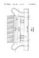
- FIG. 1schematically depicts a side view of a prior art substrate and heat sink attachment using pins for structural support.
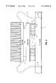
- FIG. 2is a schematic illustrating the connection of a substrate to a printed circuit board using reinforcing solder columns according to the present invention.
- FIG. 3is a schematic showing a substrate attached with reinforcing columns to a printed circuit board and having a heat sink thermally contacting a structural element of the substrate.
- FIG. 4schematically depicts process steps by which the invention may be practiced in two variants.
- FIG. 1schematically illustrates the prior art relating to the structural support for a substrate connected by a solder column array to a printed circuit board when configured with a heat sink.
- ceramic substrate 1has bonded thereto integrated circuit chip 2 , chip 2 representing an individual integrated circuit die or a capped integrated circuit device.
- Electrically conductive pads 3 and 4respectively formed on substrate 1 and FR 4 type fiber glass printed circuit board 6 , define the pattern of the solder column array for electrical input/output connections between substrate 1 and printed circuit board 6 . The connections between respective pads 3 and 4 are accomplished using solder columns 7 .
- Solder column 7are preferably formed from a 90/10 alloy of lead/tin solder, namely, high melting temperature solder, with a nominal height in the range of 0.08 inches and a nominal diameter of 0.02 inches. Solder columns 7 are attached to pads 3 of substrate 1 using either of two techniques. One process involves a high temperature reflow of the 90/10 solder columns, with the columns mounted as an array in a boat which is affixed to the substrate. An alternate technique involves the use of a low temperature solder paste deposited onto pads 3 , followed by a low temperature reflow of the paste. The lower melting temperature solder, nominally 37/63 alloy lead/tin bonds an array of 90/10 solder columns which are mounted in a supporting boat to the substrate pads. Both techniques have been in commercial use.
- solder columns 7The materially different coefficients of thermal expansion exhibited by substrate 1 and printed circuit board 6 are within the flexing capabilities of solder columns 7 given the relative aspect ratio of the columns. Unfortunately, that aspect ratio makes the columns vulnerable to compressive and/or lateral forces, such as those created by spring 8 and any movement of heat sink 9 . Since the thermal resistance between heat sink 9 and chip 2 is inversely related to the clamping pressure, the structural limitations of solder columns 7 also constrain the ability to effectively cool chip 2 when heat transfer is initiated by spring 8 .
- Pins 11are composed of kovar or cu-sil, exhibit a high compressive strength, and have minimal creep in relation to solder columns 7 .
- Pins 11are bonded to substrate 1 by brazing and extend into holes 12 drilled through printed circuit board 6 .
- the use of such pins to support substrate 1requires the additional manufacturing steps to braze attach pins 11 , drill holes 12 in printed circuit board 6 , and to align pins 11 with holes 12 when mounting substrate 1 .
- the rigidity of the elements involvedmandates very tight tolerances for the location of pins 11 and holes 12 .
- the present inventioneliminates the additional manufacturing steps and tolerance requirements by extending the basic column attachment process to further support substrate 1 , especially in the presence of heat sink 9 .
- the inventionis applicable to situations in which substrate 1 is the ceramic base of integrated circuit die 2 , whether die 2 is capped or exposed. For a flip-chip application, die 2 is bonded to substrate 1 using solder bumps.
- heat sink 9 in FIG. 1is shown compressively affixed to a structural element, chip 2 of the substrate using spring 8 , the invention is also applicable to situations in which the heat sink is bonded directly to a structural element of the substrate, or is compressively connected to such structural element using a mechanically adjustable clamp.
- Key to the inventionis the ability to materially increase the structural integrity of the interface between substrate 1 and printed circuit board 6 for shock and vibration environments within the framework of conventional solder column fabrication practices.
- FIGS. 2 and 3illustrate the aspects of the present invention in connecting substrate 1 to printed circuit board 6 .
- pads 3 of substrate 1each have a solder column 7 attached by solder reflow.
- substrate 1also includes pads 13 situated along the perimeter of substrate 1 , typically in the corners of the substrate, which have attached thereto individual solder columns 14 .
- Columns 14are composed of high melting temperature solder, for example the earlier noted 90/10 alloy, and are attached when electrical signal columns 7 are bonded to pads 3 of substrate 1 .
- Solder columns 14 along the perimeter of substrate 1provide the structural support while the array of solder columns 7 provide the high density electrical connections.
- columns 14are in the range of 0.08 inches or greater in diameter while matching the height of columns 7 .
- solder paste 17is composed of flux and nominal 37/63 composition lead/tin solder having a melting temperature of approximately 180 degrees C.
- FIG. 3schematically illustrates the structural arrangement after heat sink 9 is mounted.
- Heat sink 9can be held in place using spring 8 extending through holes 18 in printed circuit board 6 , or by direct bonding between heat sink 9 and chip 2 using thermal epoxy material.
- Support and spacing solder columns 14are bonded to printed circuit board pads 16 by reflowed solder 19 while the array of columns 7 are electrically connected to pads 4 on printed circuit board 6 with reflowed solder 21 .
- FIG. 4schematically illustrates alternate operations for attaching solder columns to the substrate.
- the descriptions in the various blocksare relatively self explanatory.
- low temperature solderis used to attach the solder columns to the substrate, including both the thin electrically signal solder columns and the structural supporting solder columns, all the columns are loaded in a common boat, solder paste is deposited on the substrate pads, and the solder paste is reflowed at 210-220 degrees C.
- solder columnsthemselves are reflowed as an aspect of the attachment to the substrate
- the reflowis performed without solder paste but at the materially higher temperature of approximately 350-360 degrees C. Therefore, both types of solder columns are attached simultaneously both to the substrate and to the printed circuit board.
- structural support solder columns 14do not need to be circular in cross-section.
- the inventionfully contemplates square or other cross-sections, as the substrate area and load conditions dictate.
- chip 2may be an actual integrated circuit die or the cap of an integrated circuit die. In either case, it constitutes a structural element of substrate 1 for purposes of transferring heat to heat sink 9 .
- columns 14are fully capable of transmitting electrical power or functional input/output signals, and are likely to be used for such as the pin-out needs of integrated circuit devices increase.
- the inventionhas been described in the context of a substrate, typically ceramic, onto which an integrated circuit die is attached, the fundamental concepts are fully applicable to a situation in which the substrate itself is a flip-chip device.
- the columnsare bonded directly to the flip-chip die pads, and the heat sink is thermally connected to the back side of the flip-chip die.
- Such a flip-chip devicecan be connected directly to an organic printed circuit board, a ceramic carrier, or other die wiring package.
Landscapes
- Engineering & Computer Science (AREA)
- Microelectronics & Electronic Packaging (AREA)
- Physics & Mathematics (AREA)
- Computer Hardware Design (AREA)
- Condensed Matter Physics & Semiconductors (AREA)
- General Physics & Mathematics (AREA)
- Power Engineering (AREA)
- Manufacturing & Machinery (AREA)
- Thermal Sciences (AREA)
- Cooling Or The Like Of Semiconductors Or Solid State Devices (AREA)
- Cooling Or The Like Of Electrical Apparatus (AREA)
- Combinations Of Printed Boards (AREA)
- Structure Of Printed Boards (AREA)
Abstract
Description
Claims (14)
Priority Applications (5)
| Application Number | Priority Date | Filing Date | Title |
|---|---|---|---|
| US08/688,073US6395991B1 (en) | 1996-07-29 | 1996-07-29 | Column grid array substrate attachment with heat sink stress relief |
| KR1019970021697AKR100264638B1 (en) | 1996-07-29 | 1997-05-29 | Column grid array substrate attachment with heat sink stress relief |
| EP97305034AEP0822738B1 (en) | 1996-07-29 | 1997-07-09 | Column array connections |
| DE69721148TDE69721148T2 (en) | 1996-07-29 | 1997-07-09 | Columns grid connections |
| JP19097497AJP3368177B2 (en) | 1996-07-29 | 1997-07-16 | Apparatus and method for providing effective heat sink contact to structural elements of a substrate |
Applications Claiming Priority (1)
| Application Number | Priority Date | Filing Date | Title |
|---|---|---|---|
| US08/688,073US6395991B1 (en) | 1996-07-29 | 1996-07-29 | Column grid array substrate attachment with heat sink stress relief |
Publications (1)
| Publication Number | Publication Date |
|---|---|
| US6395991B1true US6395991B1 (en) | 2002-05-28 |
Family
ID=24763007
Family Applications (1)
| Application Number | Title | Priority Date | Filing Date |
|---|---|---|---|
| US08/688,073Expired - LifetimeUS6395991B1 (en) | 1996-07-29 | 1996-07-29 | Column grid array substrate attachment with heat sink stress relief |
Country Status (5)
| Country | Link |
|---|---|
| US (1) | US6395991B1 (en) |
| EP (1) | EP0822738B1 (en) |
| JP (1) | JP3368177B2 (en) |
| KR (1) | KR100264638B1 (en) |
| DE (1) | DE69721148T2 (en) |
Cited By (28)
| Publication number | Priority date | Publication date | Assignee | Title |
|---|---|---|---|---|
| US20010042910A1 (en)* | 2000-01-06 | 2001-11-22 | Eng Klan Teng | Vertical ball grid array integrated circuit package |
| US20020104641A1 (en)* | 2000-03-14 | 2002-08-08 | Searls Damion T. | Apparatus and method for passive phase change thermal management |
| US20030094306A1 (en)* | 2001-11-16 | 2003-05-22 | Deeney Jeffrey L. | Method and apparatus for supporting a circuit component having solder column interconnects using external support |
| US6727718B2 (en)* | 1998-03-11 | 2004-04-27 | Fujistu Limited | Electronic component package, printed circuit board, and method of inspecting the printed circuit board |
| US20040134680A1 (en)* | 2003-01-09 | 2004-07-15 | Xiang Dai | Use of perimeter stops to support solder interconnects between integrated circuit assembly components |
| US6798663B1 (en)* | 2003-04-21 | 2004-09-28 | Hewlett Packard Development Company, L.P. | Heat sink hold-down with fan-module attach location |
| US20040207985A1 (en)* | 2003-04-21 | 2004-10-21 | Delano Andrew D. | Variable-gap thermal-interface device |
| US20040226688A1 (en)* | 2003-04-30 | 2004-11-18 | Arthur Fong | Application specific apparatus for dissipating heat from multiple electronic components |
| US20040233710A1 (en)* | 2003-05-23 | 2004-11-25 | Perner Frederick A. | Method and system for data communication on a chip |
| US20040232561A1 (en)* | 2003-05-22 | 2004-11-25 | Texas Instruments Incorporated | System and method to increase die stand-off height |
| US20040250989A1 (en)* | 2003-02-11 | 2004-12-16 | Yun-Hyeok Im | Clothespin type heat dissipating apparatus for semiconductor module |
| US20050117296A1 (en)* | 2003-12-02 | 2005-06-02 | Chung-Ju Wu | Ball grid array package with heat sink device |
| US6927491B1 (en)* | 1998-12-04 | 2005-08-09 | Nec Corporation | Back electrode type electronic part and electronic assembly with the same mounted on printed circuit board |
| US20060192293A1 (en)* | 2005-02-25 | 2006-08-31 | Fujitsu Limited | Electronic device, standoff member, and method of manufacturing electronic device |
| US20060238990A1 (en)* | 2005-03-21 | 2006-10-26 | Ephraim Suhir | Apparatus for attaching a cooling structure to an integrated circuit |
| US20060270116A1 (en)* | 2003-08-25 | 2006-11-30 | Nanoconduction, Inc. | System and method using self-assembled nano structures in the design and fabrication of an integrated circuit micro-cooler |
| US20070114658A1 (en)* | 2004-08-24 | 2007-05-24 | Carlos Dangelo | Integrated Circuit Micro-Cooler with Double-Sided Tubes of a CNT Array |
| US20070114657A1 (en)* | 2003-08-25 | 2007-05-24 | Carlos Dangelo | Integrated circuit micro-cooler having multi-layers of tubes of a cnt array |
| US20080096293A1 (en)* | 2006-10-24 | 2008-04-24 | Ephraim Suhir | Method and Apparatus for Evaluation and Improvement of Mechanical and Thermal Properties of CNT/CNF Arrays |
| US20080128116A1 (en)* | 2003-08-25 | 2008-06-05 | Carlos Dangelo | Vapor chamber heat sink having a carbon nanotube fluid interface |
| US20090134529A1 (en)* | 2007-11-28 | 2009-05-28 | Kabushiki Kaisha Toshiba | Circuit board module, electric device, and method for producing circuit board module |
| US20110001232A1 (en)* | 2005-09-14 | 2011-01-06 | Htc Beteiligungs Gmbh | Flip-Chip Module and Method for the Production Thereof |
| CN102148215A (en)* | 2011-01-21 | 2011-08-10 | 哈尔滨理工大学 | Interconnection structure for improving reliability of soldering spot of soft soldering of CCGA (Ceramic Column Grid Array) device and implementation method |
| CN102280415A (en)* | 2010-06-14 | 2011-12-14 | 富士通株式会社 | Packaging structure, printed circuit board assembly and fixing method |
| US8415792B2 (en) | 2010-08-04 | 2013-04-09 | International Business Machines Corporation | Electrical contact alignment posts |
| US20160057861A1 (en)* | 2014-08-19 | 2016-02-25 | International Business Machines Corporation | Metallized particle interconnect with solder components |
| CN110176437A (en)* | 2019-05-31 | 2019-08-27 | 合肥圣达电子科技实业有限公司 | A kind of thin space ceramic wiring terminal and preparation method thereof |
| US20210329793A1 (en)* | 2018-09-14 | 2021-10-21 | Continental Automotive Gmbh | Method for producing a circuit board arrangement, and circuit board arrangement |
Families Citing this family (6)
| Publication number | Priority date | Publication date | Assignee | Title |
|---|---|---|---|---|
| AU5305799A (en)* | 1998-09-02 | 2000-03-27 | Ibiden Co. Ltd. | Electronic part module mounted on socket |
| KR100598329B1 (en)* | 1999-06-12 | 2006-07-10 | 주식회사 하이닉스반도체 | Semiconductor package and manufacturing method |
| DE102005043910A1 (en)* | 2005-09-14 | 2007-03-15 | Weissbach, Ernst-A. | Flip-chip module comprises a semiconductor chip having contact columns on a surface, a substrate with contact sites joined to the free ends of the contact columns and a rigid spacer arranged between the substrate and chip |
| KR100938867B1 (en) | 2007-09-07 | 2010-01-27 | 이상수 | Heat sink and heating element assembly for food waste drying processor and manufacturing method thereof |
| CN107139313B (en)* | 2017-06-09 | 2019-03-22 | 长安大学 | A kind of intelligence tablet press machine |
| EP4270479A4 (en)* | 2021-01-28 | 2024-07-10 | Huawei Technologies Co., Ltd. | INTERCONNECTION ARRANGEMENT, PLATE LEVEL ARCHITECTURE AND COMPUTER DEVICE |
Citations (33)
| Publication number | Priority date | Publication date | Assignee | Title |
|---|---|---|---|---|
| US3871015A (en) | 1969-08-14 | 1975-03-11 | Ibm | Flip chip module with non-uniform connector joints |
| US3932934A (en) | 1974-09-16 | 1976-01-20 | Amp Incorporated | Method of connecting terminal posts of a connector to a circuit board |
| US4413308A (en) | 1981-08-31 | 1983-11-01 | Bell Telephone Laboratories, Incorporated | Printed wiring board construction |
| US4509096A (en) | 1983-02-22 | 1985-04-02 | Smiths Industries Public Limited Company | Chip-carrier substrates |
| US4561011A (en)* | 1982-10-05 | 1985-12-24 | Mitsubishi Denki Kabushiki Kaisha | Dimensionally stable semiconductor device |
| US4604644A (en) | 1985-01-28 | 1986-08-05 | International Business Machines Corporation | Solder interconnection structure for joining semiconductor devices to substrates that have improved fatigue life, and process for making |
| US4664309A (en) | 1983-06-30 | 1987-05-12 | Raychem Corporation | Chip mounting device |
| US4705205A (en) | 1983-06-30 | 1987-11-10 | Raychem Corporation | Chip carrier mounting device |
| US4878611A (en) | 1986-05-30 | 1989-11-07 | American Telephone And Telegraph Company, At&T Bell Laboratories | Process for controlling solder joint geometry when surface mounting a leadless integrated circuit package on a substrate |
| US4914814A (en) | 1989-05-04 | 1990-04-10 | International Business Machines Corporation | Process of fabricating a circuit package |
| US4927697A (en) | 1987-11-28 | 1990-05-22 | British Aerospace Public Limited Company | Surface mounting leadless components on conductor pattern supporting substrates |
| US5001829A (en) | 1990-01-02 | 1991-03-26 | General Electric Company | Method for connecting a leadless chip carrier to a substrate |
| US5088007A (en) | 1991-04-04 | 1992-02-11 | Motorola, Inc. | Compliant solder interconnection |
| US5108027A (en) | 1989-05-16 | 1992-04-28 | Gec-Marconi Limited | Flip chip solder bond structure for devices with gold based metallization |
| US5222014A (en) | 1992-03-02 | 1993-06-22 | Motorola, Inc. | Three-dimensional multi-chip pad array carrier |
| US5233504A (en) | 1990-12-06 | 1993-08-03 | Motorola, Inc. | Noncollapsing multisolder interconnection |
| US5251806A (en) | 1990-06-19 | 1993-10-12 | International Business Machines Corporation | Method of forming dual height solder interconnections |
| US5324892A (en) | 1992-08-07 | 1994-06-28 | International Business Machines Corporation | Method of fabricating an electronic interconnection |
| US5349495A (en) | 1989-06-23 | 1994-09-20 | Vlsi Technology, Inc. | System for securing and electrically connecting a semiconductor chip to a substrate |
| US5397921A (en) | 1993-09-03 | 1995-03-14 | Advanced Semiconductor Assembly Technology | Tab grid array |
| US5400950A (en) | 1994-02-22 | 1995-03-28 | Delco Electronics Corporation | Method for controlling solder bump height for flip chip integrated circuit devices |
| US5490040A (en)* | 1993-12-22 | 1996-02-06 | International Business Machines Corporation | Surface mount chip package having an array of solder ball contacts arranged in a circle and conductive pin contacts arranged outside the circular array |
| US5498903A (en) | 1992-12-21 | 1996-03-12 | Sgs-Thomson Microelectronics, Inc. | Surface mountable integrated circuit package with integrated battery mount |
| US5541450A (en) | 1994-11-02 | 1996-07-30 | Motorola, Inc. | Low-profile ball-grid array semiconductor package |
| US5551627A (en) | 1994-09-29 | 1996-09-03 | Motorola, Inc. | Alloy solder connect assembly and method of connection |
| US5598036A (en)* | 1995-06-15 | 1997-01-28 | Industrial Technology Research Institute | Ball grid array having reduced mechanical stress |
| US5639696A (en) | 1996-01-31 | 1997-06-17 | Lsi Logic Corporation | Microelectronic integrated circuit mounted on circuit board with solder column grid array interconnection, and method of fabricating the solder column grid array |
| US5641990A (en) | 1994-09-15 | 1997-06-24 | Intel Corporation | Laminated solder column |
| US5675183A (en) | 1995-07-12 | 1997-10-07 | Dell Usa Lp | Hybrid multichip module and methods of fabricating same |
| US5718367A (en) | 1995-11-21 | 1998-02-17 | International Business Machines Corporation | Mold transfer apparatus and method |
| US5821161A (en) | 1997-05-01 | 1998-10-13 | International Business Machines Corporation | Cast metal seal for semiconductor substrates and process thereof |
| US5881945A (en) | 1997-04-30 | 1999-03-16 | International Business Machines Corporation | Multi-layer solder seal band for semiconductor substrates and process |
| US5881944A (en) | 1997-04-30 | 1999-03-16 | International Business Machines Corporation | Multi-layer solder seal band for semiconductor substrates |
Family Cites Families (4)
| Publication number | Priority date | Publication date | Assignee | Title |
|---|---|---|---|---|
| US4545610A (en)* | 1983-11-25 | 1985-10-08 | International Business Machines Corporation | Method for forming elongated solder connections between a semiconductor device and a supporting substrate |
| JP2974436B2 (en)* | 1991-02-26 | 1999-11-10 | シチズン時計株式会社 | Solder bump formation method |
| US5591941A (en)* | 1993-10-28 | 1997-01-07 | International Business Machines Corporation | Solder ball interconnected assembly |
| FR2735648B1 (en)* | 1995-06-13 | 1997-07-11 | Bull Sa | COOLING METHOD OF AN INTEGRATED CIRCUIT MOUNTED IN A HOUSING |
- 1996
- 1996-07-29USUS08/688,073patent/US6395991B1/ennot_activeExpired - Lifetime
- 1997
- 1997-05-29KRKR1019970021697Apatent/KR100264638B1/ennot_activeExpired - Fee Related
- 1997-07-09EPEP97305034Apatent/EP0822738B1/ennot_activeExpired - Lifetime
- 1997-07-09DEDE69721148Tpatent/DE69721148T2/ennot_activeExpired - Fee Related
- 1997-07-16JPJP19097497Apatent/JP3368177B2/ennot_activeExpired - Fee Related
Patent Citations (33)
| Publication number | Priority date | Publication date | Assignee | Title |
|---|---|---|---|---|
| US3871015A (en) | 1969-08-14 | 1975-03-11 | Ibm | Flip chip module with non-uniform connector joints |
| US3932934A (en) | 1974-09-16 | 1976-01-20 | Amp Incorporated | Method of connecting terminal posts of a connector to a circuit board |
| US4413308A (en) | 1981-08-31 | 1983-11-01 | Bell Telephone Laboratories, Incorporated | Printed wiring board construction |
| US4561011A (en)* | 1982-10-05 | 1985-12-24 | Mitsubishi Denki Kabushiki Kaisha | Dimensionally stable semiconductor device |
| US4509096A (en) | 1983-02-22 | 1985-04-02 | Smiths Industries Public Limited Company | Chip-carrier substrates |
| US4664309A (en) | 1983-06-30 | 1987-05-12 | Raychem Corporation | Chip mounting device |
| US4705205A (en) | 1983-06-30 | 1987-11-10 | Raychem Corporation | Chip carrier mounting device |
| US4604644A (en) | 1985-01-28 | 1986-08-05 | International Business Machines Corporation | Solder interconnection structure for joining semiconductor devices to substrates that have improved fatigue life, and process for making |
| US4878611A (en) | 1986-05-30 | 1989-11-07 | American Telephone And Telegraph Company, At&T Bell Laboratories | Process for controlling solder joint geometry when surface mounting a leadless integrated circuit package on a substrate |
| US4927697A (en) | 1987-11-28 | 1990-05-22 | British Aerospace Public Limited Company | Surface mounting leadless components on conductor pattern supporting substrates |
| US4914814A (en) | 1989-05-04 | 1990-04-10 | International Business Machines Corporation | Process of fabricating a circuit package |
| US5108027A (en) | 1989-05-16 | 1992-04-28 | Gec-Marconi Limited | Flip chip solder bond structure for devices with gold based metallization |
| US5349495A (en) | 1989-06-23 | 1994-09-20 | Vlsi Technology, Inc. | System for securing and electrically connecting a semiconductor chip to a substrate |
| US5001829A (en) | 1990-01-02 | 1991-03-26 | General Electric Company | Method for connecting a leadless chip carrier to a substrate |
| US5251806A (en) | 1990-06-19 | 1993-10-12 | International Business Machines Corporation | Method of forming dual height solder interconnections |
| US5233504A (en) | 1990-12-06 | 1993-08-03 | Motorola, Inc. | Noncollapsing multisolder interconnection |
| US5088007A (en) | 1991-04-04 | 1992-02-11 | Motorola, Inc. | Compliant solder interconnection |
| US5222014A (en) | 1992-03-02 | 1993-06-22 | Motorola, Inc. | Three-dimensional multi-chip pad array carrier |
| US5324892A (en) | 1992-08-07 | 1994-06-28 | International Business Machines Corporation | Method of fabricating an electronic interconnection |
| US5498903A (en) | 1992-12-21 | 1996-03-12 | Sgs-Thomson Microelectronics, Inc. | Surface mountable integrated circuit package with integrated battery mount |
| US5397921A (en) | 1993-09-03 | 1995-03-14 | Advanced Semiconductor Assembly Technology | Tab grid array |
| US5490040A (en)* | 1993-12-22 | 1996-02-06 | International Business Machines Corporation | Surface mount chip package having an array of solder ball contacts arranged in a circle and conductive pin contacts arranged outside the circular array |
| US5400950A (en) | 1994-02-22 | 1995-03-28 | Delco Electronics Corporation | Method for controlling solder bump height for flip chip integrated circuit devices |
| US5641990A (en) | 1994-09-15 | 1997-06-24 | Intel Corporation | Laminated solder column |
| US5551627A (en) | 1994-09-29 | 1996-09-03 | Motorola, Inc. | Alloy solder connect assembly and method of connection |
| US5541450A (en) | 1994-11-02 | 1996-07-30 | Motorola, Inc. | Low-profile ball-grid array semiconductor package |
| US5598036A (en)* | 1995-06-15 | 1997-01-28 | Industrial Technology Research Institute | Ball grid array having reduced mechanical stress |
| US5675183A (en) | 1995-07-12 | 1997-10-07 | Dell Usa Lp | Hybrid multichip module and methods of fabricating same |
| US5718367A (en) | 1995-11-21 | 1998-02-17 | International Business Machines Corporation | Mold transfer apparatus and method |
| US5639696A (en) | 1996-01-31 | 1997-06-17 | Lsi Logic Corporation | Microelectronic integrated circuit mounted on circuit board with solder column grid array interconnection, and method of fabricating the solder column grid array |
| US5881945A (en) | 1997-04-30 | 1999-03-16 | International Business Machines Corporation | Multi-layer solder seal band for semiconductor substrates and process |
| US5881944A (en) | 1997-04-30 | 1999-03-16 | International Business Machines Corporation | Multi-layer solder seal band for semiconductor substrates |
| US5821161A (en) | 1997-05-01 | 1998-10-13 | International Business Machines Corporation | Cast metal seal for semiconductor substrates and process thereof |
Non-Patent Citations (2)
| Title |
|---|
| IBM Technical Disclosure Bulletin, vol. 32, No. 8A, Jan. 1990, "Latchless Pneumatic Impact Actuator", pp. 483-486. |
| IBM Technical Disclosure Bulletin, vol. 38, No. 02, Feb. 1995, "Surface Mount Heat Sink for Solder Ball Connect Modules and C4 Chip to Card Attach", p. 419. |
Cited By (54)
| Publication number | Priority date | Publication date | Assignee | Title |
|---|---|---|---|---|
| US6727718B2 (en)* | 1998-03-11 | 2004-04-27 | Fujistu Limited | Electronic component package, printed circuit board, and method of inspecting the printed circuit board |
| US6927491B1 (en)* | 1998-12-04 | 2005-08-09 | Nec Corporation | Back electrode type electronic part and electronic assembly with the same mounted on printed circuit board |
| US20010042910A1 (en)* | 2000-01-06 | 2001-11-22 | Eng Klan Teng | Vertical ball grid array integrated circuit package |
| US7886809B2 (en) | 2000-03-14 | 2011-02-15 | Intel Corporation | Apparatus and method for passive phase change thermal management |
| US20020104641A1 (en)* | 2000-03-14 | 2002-08-08 | Searls Damion T. | Apparatus and method for passive phase change thermal management |
| US20080066890A1 (en)* | 2000-03-14 | 2008-03-20 | Intel Corporation | Apparatus and method for passive phase change thermal management |
| US6672370B2 (en)* | 2000-03-14 | 2004-01-06 | Intel Corporation | Apparatus and method for passive phase change thermal management |
| US7316265B2 (en)* | 2000-03-14 | 2008-01-08 | Intel Corporation | Method for passive phase change thermal management |
| US20050051300A1 (en)* | 2000-03-14 | 2005-03-10 | Intel Corporation. | Apparatus and method for passive phase change thermal management |
| US6710264B2 (en)* | 2001-11-16 | 2004-03-23 | Hewlett-Packard Development Company, L.P. | Method and apparatus for supporting a circuit component having solder column interconnects using external support |
| US20040035606A1 (en)* | 2001-11-16 | 2004-02-26 | Deeney Jeffrey L. | Method and apparatus for supporting a circuit component having solder column interconnects using an external support |
| US7434309B2 (en) | 2001-11-16 | 2008-10-14 | Hewlett-Packard Development Company, L.P. | Method and apparatus for supporting a circuit component having solder column interconnects using an external support |
| US20030094306A1 (en)* | 2001-11-16 | 2003-05-22 | Deeney Jeffrey L. | Method and apparatus for supporting a circuit component having solder column interconnects using external support |
| US20040134680A1 (en)* | 2003-01-09 | 2004-07-15 | Xiang Dai | Use of perimeter stops to support solder interconnects between integrated circuit assembly components |
| US20040250989A1 (en)* | 2003-02-11 | 2004-12-16 | Yun-Hyeok Im | Clothespin type heat dissipating apparatus for semiconductor module |
| US20040207986A1 (en)* | 2003-04-21 | 2004-10-21 | Rubenstein Brandon A. | Heat sink hold-down with fan-module attach location |
| US20040207985A1 (en)* | 2003-04-21 | 2004-10-21 | Delano Andrew D. | Variable-gap thermal-interface device |
| US6798663B1 (en)* | 2003-04-21 | 2004-09-28 | Hewlett Packard Development Company, L.P. | Heat sink hold-down with fan-module attach location |
| US7480143B2 (en) | 2003-04-21 | 2009-01-20 | Hewlett-Packard Development Company, L.P. | Variable-gap thermal-interface device |
| US20040226688A1 (en)* | 2003-04-30 | 2004-11-18 | Arthur Fong | Application specific apparatus for dissipating heat from multiple electronic components |
| US20040232561A1 (en)* | 2003-05-22 | 2004-11-25 | Texas Instruments Incorporated | System and method to increase die stand-off height |
| US7224071B2 (en)* | 2003-05-22 | 2007-05-29 | Texas Instruments Incorporated | System and method to increase die stand-off height |
| US20040233710A1 (en)* | 2003-05-23 | 2004-11-25 | Perner Frederick A. | Method and system for data communication on a chip |
| US8039953B2 (en) | 2003-08-25 | 2011-10-18 | Samsung Electronics Co., Ltd. | System and method using self-assembled nano structures in the design and fabrication of an integrated circuit micro-cooler |
| US20070114657A1 (en)* | 2003-08-25 | 2007-05-24 | Carlos Dangelo | Integrated circuit micro-cooler having multi-layers of tubes of a cnt array |
| US20060270116A1 (en)* | 2003-08-25 | 2006-11-30 | Nanoconduction, Inc. | System and method using self-assembled nano structures in the design and fabrication of an integrated circuit micro-cooler |
| US20080128116A1 (en)* | 2003-08-25 | 2008-06-05 | Carlos Dangelo | Vapor chamber heat sink having a carbon nanotube fluid interface |
| US7538422B2 (en) | 2003-08-25 | 2009-05-26 | Nanoconduction Inc. | Integrated circuit micro-cooler having multi-layers of tubes of a CNT array |
| US7732918B2 (en) | 2003-08-25 | 2010-06-08 | Nanoconduction, Inc. | Vapor chamber heat sink having a carbon nanotube fluid interface |
| US20050117296A1 (en)* | 2003-12-02 | 2005-06-02 | Chung-Ju Wu | Ball grid array package with heat sink device |
| US7209354B2 (en)* | 2003-12-02 | 2007-04-24 | Silicon Intergrated Systems Corp. | Ball grid array package with heat sink device |
| US20070114658A1 (en)* | 2004-08-24 | 2007-05-24 | Carlos Dangelo | Integrated Circuit Micro-Cooler with Double-Sided Tubes of a CNT Array |
| US7838987B2 (en)* | 2005-02-25 | 2010-11-23 | Fujitsu Limited | Electronic device, standoff member, and method of manufacturing electronic device |
| US20060192293A1 (en)* | 2005-02-25 | 2006-08-31 | Fujitsu Limited | Electronic device, standoff member, and method of manufacturing electronic device |
| US20060238990A1 (en)* | 2005-03-21 | 2006-10-26 | Ephraim Suhir | Apparatus for attaching a cooling structure to an integrated circuit |
| US7477527B2 (en) | 2005-03-21 | 2009-01-13 | Nanoconduction, Inc. | Apparatus for attaching a cooling structure to an integrated circuit |
| US20110001232A1 (en)* | 2005-09-14 | 2011-01-06 | Htc Beteiligungs Gmbh | Flip-Chip Module and Method for the Production Thereof |
| US8026583B2 (en) | 2005-09-14 | 2011-09-27 | Htc Beteiligungs Gmbh | Flip-chip module and method for the production thereof |
| US20080096293A1 (en)* | 2006-10-24 | 2008-04-24 | Ephraim Suhir | Method and Apparatus for Evaluation and Improvement of Mechanical and Thermal Properties of CNT/CNF Arrays |
| US8048688B2 (en) | 2006-10-24 | 2011-11-01 | Samsung Electronics Co., Ltd. | Method and apparatus for evaluation and improvement of mechanical and thermal properties of CNT/CNF arrays |
| US20090134529A1 (en)* | 2007-11-28 | 2009-05-28 | Kabushiki Kaisha Toshiba | Circuit board module, electric device, and method for producing circuit board module |
| CN101448370A (en)* | 2007-11-28 | 2009-06-03 | 株式会社东芝 | Circuit board module, electric device, and method for producing the circuit board module |
| CN102280415A (en)* | 2010-06-14 | 2011-12-14 | 富士通株式会社 | Packaging structure, printed circuit board assembly and fixing method |
| EP2400824A1 (en)* | 2010-06-14 | 2011-12-28 | Fujitsu Limited | Packaging structure, printed circuit board assembly and fixing method |
| US8415792B2 (en) | 2010-08-04 | 2013-04-09 | International Business Machines Corporation | Electrical contact alignment posts |
| US8530345B2 (en) | 2010-08-04 | 2013-09-10 | International Business Machines Corporation | Electrical contact alignment posts |
| CN102148215B (en)* | 2011-01-21 | 2012-06-06 | 哈尔滨理工大学 | Interconnection structure for improving reliability of soldering spot of soft soldering of CCGA (Ceramic Column Grid Array) device and implementation method |
| CN102148215A (en)* | 2011-01-21 | 2011-08-10 | 哈尔滨理工大学 | Interconnection structure for improving reliability of soldering spot of soft soldering of CCGA (Ceramic Column Grid Array) device and implementation method |
| US20160057861A1 (en)* | 2014-08-19 | 2016-02-25 | International Business Machines Corporation | Metallized particle interconnect with solder components |
| US10588219B2 (en)* | 2014-08-19 | 2020-03-10 | International Business Machines Corporation | Metallized particle interconnect with solder components |
| US20210329793A1 (en)* | 2018-09-14 | 2021-10-21 | Continental Automotive Gmbh | Method for producing a circuit board arrangement, and circuit board arrangement |
| US12279380B2 (en)* | 2018-09-14 | 2025-04-15 | Continental Automotive Gmbh | Method for producing a circuit board arrangement |
| CN110176437A (en)* | 2019-05-31 | 2019-08-27 | 合肥圣达电子科技实业有限公司 | A kind of thin space ceramic wiring terminal and preparation method thereof |
| CN110176437B (en)* | 2019-05-31 | 2020-11-03 | 合肥圣达电子科技实业有限公司 | Narrow-spacing ceramic binding post and preparation method thereof |
Also Published As
| Publication number | Publication date |
|---|---|
| DE69721148T2 (en) | 2003-12-11 |
| EP0822738B1 (en) | 2003-04-23 |
| KR100264638B1 (en) | 2000-09-01 |
| JPH1092983A (en) | 1998-04-10 |
| EP0822738A2 (en) | 1998-02-04 |
| EP0822738A3 (en) | 1999-08-11 |
| DE69721148D1 (en) | 2003-05-28 |
| JP3368177B2 (en) | 2003-01-20 |
| KR980013574A (en) | 1998-04-30 |
Similar Documents
| Publication | Publication Date | Title |
|---|---|---|
| US6395991B1 (en) | Column grid array substrate attachment with heat sink stress relief | |
| US6053394A (en) | Column grid array substrate attachment with heat sink stress relief | |
| US6570259B2 (en) | Apparatus to reduce thermal fatigue stress on flip chip solder connections | |
| KR100247716B1 (en) | Structurally reinforced ball grid array semiconductor package and systems | |
| JP2570498B2 (en) | Integrated circuit chip carrier | |
| US6562653B1 (en) | Silicon interposer and multi-chip-module (MCM) with through substrate vias | |
| US6002168A (en) | Microelectronic component with rigid interposer | |
| US5386341A (en) | Flexible substrate folded in a U-shape with a rigidizer plate located in the notch of the U-shape | |
| US5222014A (en) | Three-dimensional multi-chip pad array carrier | |
| US5801072A (en) | Method of packaging integrated circuits | |
| US6339254B1 (en) | Stacked flip-chip integrated circuit assemblage | |
| US6573609B2 (en) | Microelectronic component with rigid interposer | |
| US6552267B2 (en) | Microelectronic assembly with stiffening member | |
| US6184570B1 (en) | Integrated circuit dies including thermal stress reducing grooves and microelectronic packages utilizing the same | |
| HK1004352B (en) | Stackable three-dimensional multiple chip semiconductor device and method for making the same | |
| KR19980032206A (en) | High Performance Multichip Module Package | |
| US7015066B2 (en) | Method for stress reduction in flip chip bump during flip chip mounting and underfill process steps of making a microelectronic assembly | |
| US7462939B2 (en) | Interposer for compliant interfacial coupling | |
| US6943060B1 (en) | Method for fabricating integrated circuit package with solder bumps | |
| US6351389B1 (en) | Device and method for packaging an electronic device | |
| JP2001267699A (en) | Chip scale packaging with coincident cte on printed circuit board | |
| JP2812238B2 (en) | Mounting method of LSI package having metal bump | |
| US20030209798A1 (en) | Apparatus for providing mechanical support to a column grid array package | |
| US7851916B2 (en) | Strain silicon wafer with a crystal orientation (100) in flip chip BGA package | |
| JPH0331086Y2 (en) |
Legal Events
| Date | Code | Title | Description |
|---|---|---|---|
| AS | Assignment | Owner name:INTERNATIONAL BUSINESS MACHINES CORPORATION, NEW Y Free format text:ASSIGNMENT OF ASSIGNORS INTEREST;ASSIGNORS:DOCKERTY, ROBERT C.;FRAGA, RONALD M.;RAMIREZ, CIRO N.;AND OTHERS;REEL/FRAME:008201/0393;SIGNING DATES FROM 19960627 TO 19960717 | |
| STCF | Information on status: patent grant | Free format text:PATENTED CASE | |
| CC | Certificate of correction | ||
| FPAY | Fee payment | Year of fee payment:4 | |
| FPAY | Fee payment | Year of fee payment:8 | |
| REMI | Maintenance fee reminder mailed | ||
| FPAY | Fee payment | Year of fee payment:12 | |
| SULP | Surcharge for late payment | Year of fee payment:11 | |
| AS | Assignment | Owner name:GLOBALFOUNDRIES U.S. 2 LLC, NEW YORK Free format text:ASSIGNMENT OF ASSIGNORS INTEREST;ASSIGNOR:INTERNATIONAL BUSINESS MACHINES CORPORATION;REEL/FRAME:036550/0001 Effective date:20150629 | |
| AS | Assignment | Owner name:GLOBALFOUNDRIES INC., CAYMAN ISLANDS Free format text:ASSIGNMENT OF ASSIGNORS INTEREST;ASSIGNORS:GLOBALFOUNDRIES U.S. 2 LLC;GLOBALFOUNDRIES U.S. INC.;REEL/FRAME:036779/0001 Effective date:20150910 | |
| AS | Assignment | Owner name:GLOBALFOUNDRIES U.S. INC., NEW YORK Free format text:RELEASE BY SECURED PARTY;ASSIGNOR:WILMINGTON TRUST, NATIONAL ASSOCIATION;REEL/FRAME:056987/0001 Effective date:20201117 |