US6395613B1 - Semiconductor processing methods of forming a plurality of capacitors on a substrate, bit line contacts and method of forming bit line contacts - Google Patents
Semiconductor processing methods of forming a plurality of capacitors on a substrate, bit line contacts and method of forming bit line contactsDownload PDFInfo
- Publication number
- US6395613B1 US6395613B1US09/651,816US65181600AUS6395613B1US 6395613 B1US6395613 B1US 6395613B1US 65181600 AUS65181600 AUS 65181600AUS 6395613 B1US6395613 B1US 6395613B1
- Authority
- US
- United States
- Prior art keywords
- forming
- containers
- dielectric
- openings
- sidewall
- Prior art date
- Legal status (The legal status is an assumption and is not a legal conclusion. Google has not performed a legal analysis and makes no representation as to the accuracy of the status listed.)
- Expired - Lifetime
Links
Images


Classifications
- H—ELECTRICITY
- H10—SEMICONDUCTOR DEVICES; ELECTRIC SOLID-STATE DEVICES NOT OTHERWISE PROVIDED FOR
- H10D—INORGANIC ELECTRIC SEMICONDUCTOR DEVICES
- H10D1/00—Resistors, capacitors or inductors
- H10D1/01—Manufacture or treatment
- H10D1/041—Manufacture or treatment of capacitors having no potential barriers
- H10D1/042—Manufacture or treatment of capacitors having no potential barriers using deposition processes to form electrode extensions
- H—ELECTRICITY
- H01—ELECTRIC ELEMENTS
- H01L—SEMICONDUCTOR DEVICES NOT COVERED BY CLASS H10
- H01L21/00—Processes or apparatus adapted for the manufacture or treatment of semiconductor or solid state devices or of parts thereof
- H01L21/70—Manufacture or treatment of devices consisting of a plurality of solid state components formed in or on a common substrate or of parts thereof; Manufacture of integrated circuit devices or of parts thereof
- H01L21/71—Manufacture of specific parts of devices defined in group H01L21/70
- H01L21/768—Applying interconnections to be used for carrying current between separate components within a device comprising conductors and dielectrics
- H01L21/76801—Applying interconnections to be used for carrying current between separate components within a device comprising conductors and dielectrics characterised by the formation and the after-treatment of the dielectrics, e.g. smoothing
- H01L21/76802—Applying interconnections to be used for carrying current between separate components within a device comprising conductors and dielectrics characterised by the formation and the after-treatment of the dielectrics, e.g. smoothing by forming openings in dielectrics
- H01L21/76816—Aspects relating to the layout of the pattern or to the size of vias or trenches
- H—ELECTRICITY
- H01—ELECTRIC ELEMENTS
- H01L—SEMICONDUCTOR DEVICES NOT COVERED BY CLASS H10
- H01L21/00—Processes or apparatus adapted for the manufacture or treatment of semiconductor or solid state devices or of parts thereof
- H01L21/70—Manufacture or treatment of devices consisting of a plurality of solid state components formed in or on a common substrate or of parts thereof; Manufacture of integrated circuit devices or of parts thereof
- H01L21/71—Manufacture of specific parts of devices defined in group H01L21/70
- H01L21/768—Applying interconnections to be used for carrying current between separate components within a device comprising conductors and dielectrics
- H01L21/76801—Applying interconnections to be used for carrying current between separate components within a device comprising conductors and dielectrics characterised by the formation and the after-treatment of the dielectrics, e.g. smoothing
- H01L21/76829—Applying interconnections to be used for carrying current between separate components within a device comprising conductors and dielectrics characterised by the formation and the after-treatment of the dielectrics, e.g. smoothing characterised by the formation of thin functional dielectric layers, e.g. dielectric etch-stop, barrier, capping or liner layers
- H01L21/76831—Applying interconnections to be used for carrying current between separate components within a device comprising conductors and dielectrics characterised by the formation and the after-treatment of the dielectrics, e.g. smoothing characterised by the formation of thin functional dielectric layers, e.g. dielectric etch-stop, barrier, capping or liner layers in via holes or trenches, e.g. non-conductive sidewall liners
- H—ELECTRICITY
- H01—ELECTRIC ELEMENTS
- H01L—SEMICONDUCTOR DEVICES NOT COVERED BY CLASS H10
- H01L21/00—Processes or apparatus adapted for the manufacture or treatment of semiconductor or solid state devices or of parts thereof
- H01L21/70—Manufacture or treatment of devices consisting of a plurality of solid state components formed in or on a common substrate or of parts thereof; Manufacture of integrated circuit devices or of parts thereof
- H01L21/71—Manufacture of specific parts of devices defined in group H01L21/70
- H01L21/768—Applying interconnections to be used for carrying current between separate components within a device comprising conductors and dielectrics
- H01L21/76801—Applying interconnections to be used for carrying current between separate components within a device comprising conductors and dielectrics characterised by the formation and the after-treatment of the dielectrics, e.g. smoothing
- H01L21/76829—Applying interconnections to be used for carrying current between separate components within a device comprising conductors and dielectrics characterised by the formation and the after-treatment of the dielectrics, e.g. smoothing characterised by the formation of thin functional dielectric layers, e.g. dielectric etch-stop, barrier, capping or liner layers
- H01L21/76832—Multiple layers
- H—ELECTRICITY
- H01—ELECTRIC ELEMENTS
- H01L—SEMICONDUCTOR DEVICES NOT COVERED BY CLASS H10
- H01L21/00—Processes or apparatus adapted for the manufacture or treatment of semiconductor or solid state devices or of parts thereof
- H01L21/70—Manufacture or treatment of devices consisting of a plurality of solid state components formed in or on a common substrate or of parts thereof; Manufacture of integrated circuit devices or of parts thereof
- H01L21/71—Manufacture of specific parts of devices defined in group H01L21/70
- H01L21/768—Applying interconnections to be used for carrying current between separate components within a device comprising conductors and dielectrics
- H01L21/76838—Applying interconnections to be used for carrying current between separate components within a device comprising conductors and dielectrics characterised by the formation and the after-treatment of the conductors
- H—ELECTRICITY
- H10—SEMICONDUCTOR DEVICES; ELECTRIC SOLID-STATE DEVICES NOT OTHERWISE PROVIDED FOR
- H10B—ELECTRONIC MEMORY DEVICES
- H10B12/00—Dynamic random access memory [DRAM] devices
- H10B12/01—Manufacture or treatment
- H10B12/02—Manufacture or treatment for one transistor one-capacitor [1T-1C] memory cells
- H10B12/03—Making the capacitor or connections thereto
- H10B12/033—Making the capacitor or connections thereto the capacitor extending over the transistor
- H—ELECTRICITY
- H10—SEMICONDUCTOR DEVICES; ELECTRIC SOLID-STATE DEVICES NOT OTHERWISE PROVIDED FOR
- H10B—ELECTRONIC MEMORY DEVICES
- H10B12/00—Dynamic random access memory [DRAM] devices
- H10B12/30—DRAM devices comprising one-transistor - one-capacitor [1T-1C] memory cells
- H10B12/48—Data lines or contacts therefor
- H10B12/485—Bit line contacts
- H—ELECTRICITY
- H10—SEMICONDUCTOR DEVICES; ELECTRIC SOLID-STATE DEVICES NOT OTHERWISE PROVIDED FOR
- H10D—INORGANIC ELECTRIC SEMICONDUCTOR DEVICES
- H10D1/00—Resistors, capacitors or inductors
- H10D1/60—Capacitors
- H10D1/68—Capacitors having no potential barriers
- H—ELECTRICITY
- H10—SEMICONDUCTOR DEVICES; ELECTRIC SOLID-STATE DEVICES NOT OTHERWISE PROVIDED FOR
- H10D—INORGANIC ELECTRIC SEMICONDUCTOR DEVICES
- H10D1/00—Resistors, capacitors or inductors
- H10D1/60—Capacitors
- H10D1/68—Capacitors having no potential barriers
- H10D1/692—Electrodes
- H10D1/711—Electrodes having non-planar surfaces, e.g. formed by texturisation
- H10D1/716—Electrodes having non-planar surfaces, e.g. formed by texturisation having vertical extensions
- H—ELECTRICITY
- H10—SEMICONDUCTOR DEVICES; ELECTRIC SOLID-STATE DEVICES NOT OTHERWISE PROVIDED FOR
- H10D—INORGANIC ELECTRIC SEMICONDUCTOR DEVICES
- H10D89/00—Aspects of integrated devices not covered by groups H10D84/00 - H10D88/00
- H10D89/10—Integrated device layouts
- H—ELECTRICITY
- H10—SEMICONDUCTOR DEVICES; ELECTRIC SOLID-STATE DEVICES NOT OTHERWISE PROVIDED FOR
- H10B—ELECTRONIC MEMORY DEVICES
- H10B12/00—Dynamic random access memory [DRAM] devices
- H10B12/30—DRAM devices comprising one-transistor - one-capacitor [1T-1C] memory cells
- H10B12/31—DRAM devices comprising one-transistor - one-capacitor [1T-1C] memory cells having a storage electrode stacked over the transistor
Definitions
- This inventionrelates to semiconductor processing methods of forming a plurality of capacitors on a substrate, bit line contacts and method of forming bit line contacts.
- Circuit devices fabricated on or over semiconductor waferstypically undergo one or more photolithographic steps during formation. During such photolithographic steps, device features can be etched using conventional techniques. The spacing between such devices is important because often times adjacent devices must be electrically isolated from one another to avoid unwanted electrical interconnections.
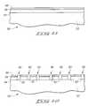
- a semiconductor wafer fragment 25includes a substrate 29 atop which a material 28 is provided.
- a plurality of patterned masking layers 26are formed atop the material 28 .
- the material 28is anisotropically etched through the patterned masking layers 26 to form lines 30 atop the substrate 29 .
- individual lines 30have respective widths L 1 which constitute the minimum photolithographic feature size available for a line.
- a separation S 1separates adjacent lines 30 across the substrate as shown.
- Such dimensionis typically only slightly larger than L 1 but could be the same as L 1 .
- the term “pitch” as used hereinis intended to be in its conventional usage, and is defined as the distance between one edge of a device and the corresponding same edge of the next adjacent device. Accordingly and in the illustrated example, the pitch P 1 between adjacent lines 30 (i.e., from the left illustrated edge of one line 30 to the left illustrated edge of the next immediately adjacent line 30 ) is equal to the sum of L 1 and S 1 .
- the inventionincludes semiconductor processing methods and related integrated circuitry in which a plurality of patterned device outlines are formed over a semiconductor substrate. Electrically insulative partitions or spacers are then formed on at least a portion of the patterned device outlines, after which a plurality of substantially identically shaped devices are formed relative to the patterned device outlines. Individual formed devices are spaced from at least one other of the devices by a distance substantially no more than a width of one of the electrically insulative spacers.
- capacitorsare formed.
- a pair of adjacent capacitor containersare formed over a substrate by etching a first capacitor container opening having at least one sidewall.
- An electrically insulative spaceris formed over the sidewall.
- a second capacitor container openingis etched selectively relative to the spacer.
- Capacitorsare then formed in the capacitor containers in a manner such that adjacent capacitors have a separation distance which is substantially no greater than the width of the spacer between the adjacent capacitors.
- a bit line contactis formed.
- the bit line contactis formed as an opening that extends through a layer formed on a substrate to a node on the substrate.
- a first dielectric sidewallis formed in the opening and coats an interior sidewall of the opening.
- a second dielectric sidewallis formed in the opening and coats an interior sidewall of the first dielectric layer.
- a conductive plugis formed within an interior sidewall of the second dielectric layer and extends through the opening to establish electrical communication to the node.
- a novel masking layoutis provided which allows capacitors to be formed in a manner which reduces device pitch by almost 50%. Such is particularly adaptive for use in fabrication of DRAM circuitry.
- FIG. 1is a top plan view of a prior art semiconductor wafer fragment atop which a plurality of masking layers are formed, and is discussed in the “Background” section above.
- FIG. 2is a side sectional view of the FIG. 1 prior art semiconductor wafer taken along line 2 — 2 in FIG. 1 .
- FIG. 3is a view of the FIG. 1 prior art semiconductor wafer fragment at processing step subsequent to that shown in FIG. 1 .
- FIG. 4is a top plan view of a semiconductor wafer fragment atop which a plurality of masking layers are formed at one processing step in accordance with one aspect of the invention.
- FIG. 5is a side view of the FIG. 4 semiconductor wafer fragment.
- FIG. 6is a view of the FIG. 5 semiconductor wafer fragment at a processing step subsequent to that shown by FIG. 5 .
- FIG. 7is a view of the FIG. 5 semiconductor wafer fragment at a processing step subsequent to that shown by FIG. 6 .
- FIG. 8is a view of the FIG. 5 semiconductor wafer fragment at a processing step subsequent to that shown by FIG. 7 .
- FIG. 9is a view of the FIG. 5 semiconductor wafer fragment at a processing step subsequent to that shown by FIG. 8 .
- FIG. 10is a top plan view of the FIG. 9 semiconductor wafer fragment.
- FIG. 11is a view of a semiconductor wafer fragment at one processing step in accordance with another aspect of the invention.
- FIG. 12is a view of the FIG. 11 semiconductor wafer fragment at a processing step subsequent to that shown by FIG. 11 .
- FIG. 13is a view of the FIG. 11 semiconductor wafer fragment at a processing step subsequent to that shown by FIG. 12 .
- FIG. 14is a view of the FIG. 11 semiconductor wafer fragment at a processing step subsequent to that shown by FIG. 13 .
- FIG. 15is a view of the FIG. 11 semiconductor wafer fragment at a processing step subsequent to that shown by FIG. 14 .
- FIG. 16is a view of the FIG. 11 semiconductor wafer fragment at a processing step subsequent to that shown by FIG. 15 .
- FIG. 17is a view of the FIG. 11 semiconductor wafer fragment at a processing step subsequent to that shown by FIG. 16 .
- FIG. 18is a view of the FIG. 11 semiconductor wafer fragment at a processing step subsequent to that shown by FIG. 17 .
- FIG. 19is a top plan view of a portion of a semiconductor mask layout in accordance with one aspect of the invention.
- FIG. 20is a top plan view of the FIG. 19 semiconductor mask layout with a portion highlighted for purposes of discussion.
- FIG. 21is a view of a portion of the FIG. 20 semiconductor mask layout highlighted portion.
- a plurality of patterned device outlines 32are photolithographically formed over a semiconductive substrate 34 .
- the term “semiconductive substrate”is defined to mean any construction comprising semiconductive material, including, but not limited to, bulk semiconductive materials such as a semiconductive wafer (either alone or in assemblies comprising other materials thereon), and semiconductive material layers (either alone or in assemblies comprising other materials).
- substraterefers to any supporting structure, including, but not limited to, the semiconductive substrates described above.
- the material constituting outlines 32may be of the type which can be etched selectively relative to the substrate 34 . Such outlines define areas over the substrate 34 in which conductive lines are to be formed.
- Such patterned device outlinesare, dimension-wise, substantially the same as those set forth with regard to the patterned masking layers 26 illustrated in FIGS. 1-3.
- an electrically insulative materialsuch as SiO 2 or Si 3 N 4 is formed over the lines 32 and the substrate 34 and is subsequently anisotropically etched to provide a plurality of sidewall spacers 36 on at least a portion, and possibly all, of the pattern device outlines 32 .
- the patterned device outlines 32define male patterns between which female patterns 38 are also formed. Accordingly, an array of alternating male/female patterns are formed over the substrate wherein the sidewall spacers 36 are formed in the female patterns 38 .
- the male patterns or patterned device outlines 32are removed by suitable etching techniques.
- the etchetches the device outlines 32 relative to the material forming spacers 36 and the substrate 34 .
- Such leaves behind a plurality of upstanding sidewall spacers 36which effectively define thin electrically insulative partitions between which a plurality of devices are to be formed. As shown, the distance or lateral spacing between adjacent spacers varies from spacer-to-spacer.
- a plurality of spaces 40 a through 40 iare provided wherein adjacent spaces, such as 40 a and 40 b , differ slightly in lateral width dimension, while alternate spaces, such as 40 a and 40 c , have substantially the same lateral width dimension.
- a conductive material 42is formed over the substrate 34 and the sidewall spacers 36 and may completely fill the spaces 40 a through 40 i .
- An example material for the layer 32is conductively doped polysilicon.
- the conductive material 42is etched back by suitable methods such as a chemical-mechanical polish (CMP) or dry etching, as is known in the art.
- CMPchemical-mechanical polish
- such devicesare conductive lines 44 which are spaced laterally from one another a distance which is no greater than a width of one of the electrically insulative sidewall spacers 36 therebetween.
- immediately adjacent conductive lines of the plurality of lines formedhave a pitch P 2 which is substantially no greater than a lateral line width L 2 plus a width W 2 of the spacer 36 which is positioned between the adjacent lines.
- P 1FIG. 1
- pitch P 2represents a reduction in pitch which approaches fifty percent. Such achieved pitch reductions are without regard to the prior art photolithographic spacing constraints imposed on semiconductor processing. As mentioned above, the spacing between adjacent spacers 36 varies from one spacer 36 to another spacer 36 . Accordingly, the pitch P 2 varies as well. It is possible for the spacing between adjacent spacers 36 to be uniform, however, so that the pitch remains constant across the substrate 34 .
- Conductive lines 44collectively define a series of conductive lines which in turn define a device array 46 of substantially identically shaped devices.
- the array 46includes the plurality of upstanding spacers 36 and the conductive lines 44 formed intermediate the spacers 36 .
- adjacent lines 44have a pitch which is substantially no greater than about the distance between a pair of adjacent spacers 36 (corresponding to the line width) plus the width of the spacer 36 therebetween.
- conductive lines 44are elongated and adjacent conductive lines 44 have different lateral line widths. Additionally, alternate lines 44 have substantially equal lateral line widths.
- line widthstems from the manner in which the anisotropically etched sidewall spacers 36 are provided over the substrate 34 , and in particular the lateral spacing of device outlines 32 (FIG. 5 ). As mentioned above, it is possible for the line widths to be substantially equal over the entire substrate 34 .
- a dashed line 48traverses the device array 46 .
- Individual elongated conductive lines 44are formed over the substrate 34 transversely along the line 48 .
- Respective alternate devices along the line 48have a substantially common width dimension therealong and respective adjacent devices have a different width dimension therealong.
- the devicescomprise capacitors, and may comprise capacitors forming part of a dynamic random access memory (DRAM) device.
- DRAMdynamic random access memory
- a plurality of bit line contactsare formed in openings etched over a substrate in one etching step, and a plurality of capacitor container openings are etched over the substrate in another two separate etching steps. Thereafter, corresponding DRAM capacitors are formed within the container openings according to known processing techniques. As so formed, and in accordance with the above-described spacer formation and pitch reduction concepts, a plurality of pairs of adjacent capacitors are formed in respective adjacent capacitor containers which are separated by no more than anisotropically etched, electrically insulative sidewall spacers as will become evident below.
- a semiconductor wafer fragment in processis shown generally at 50 and includes a layer of material 52 which may or not may be semiconductive. Transistors forming part of the DRAM circuitry array are not shown, but may be formed elevationally below the capacitors described hereafter, and contacts to these underlying structures may be formed, for example, using polysilicon plugs. Other elevational configurations as between transistors and capacitors are possible.
- a layer 54is formed over the material 52 . In one embodiment, the layer 54 is formed from borophosphosilicate glass (BPSG) to a thickness around two microns.
- a layer 56is then formed on the layer 54 . In one embodiment, the layer 56 is formed from silicon nitride to have a thickness of between 200 and 400 angstroms.
- BPSGborophosphosilicate glass
- the layer 56is formed by plasma-enhanced chemical vapor deposition. In one embodiment, the layer 56 is formed from tantalum pentoxide. A layer 58 is then formed on the layer 56 . In one embodiment, the layer 58 is formed from BPSG or from TEOS-deposited silicon dioxide. In one embodiment, the layer 58 is formed to have a thickness of between 300 and 600 Angstroms. In one embodiment, the layer 56 is formed from a material providing chemical selectivity relative to the layers 54 and 58 and thus may function as an etch stop.
- the layers 54 , 56 and 58are anisotropically etched to form bit line contact and capacitor contact openings 60 through the layers 54 , 56 and 58 .
- contact material 62is formed over the substrate and into the openings 60 .
- the contact material 62is conductively doped polysilicon.
- Such contact material 62is or may be planarized by suitable chemical-mechanical polishing or plasma etching to provide the illustrated contacts or plugs 62 .
- the plugs 62are in electrical communication with circuit nodes, such as transistors, that were previously formed according to known principles.
- the layer 58is chosen to have a thickness sufficient that if the surfaces of the plugs 62 are eroded by the planarization process, the plugs 62 together with the layer 56 still form a continuous chemical barrier to prevent etching of the layer 54 during subsequent processing steps.
- a thick layer 64is then formed over the contacts 62 and the layer 58 .
- the layer 64is formed from BPSG.
- the layer 64is formed to have a thickness of 1.5 microns, however, other thicknesses are possible.
- a photoresist pattern corresponding to bit line contact openings 66is formed on the layer 64 .
- the bit line contact openings 66are anisotropically etched through the layers 64 and 58 and may or may not continue through the layer 56 . In one embodiment, the bit line contact openings 66 have a width of between 0.16 and 0.26 microns.
- sidewall spacers 68are formed in the bit line contact openings 66 .
- the sidewall spacers 68are formed by depositing a layer of silicon nitride 200 Angstroms thick and then anisotropically etching the silicon nitride layer to remove portions of the layer formed on the contacts 62 and on other horizontal features.
- second sidewall spacers 70are then formed within the sidewall spacers 68 .
- the second sidewall spacers 70are formed by depositing up to 600 Angstroms of silicon dioxide. The silicon dioxide is then anisotropically etched to remove the silicon dioxide from the contacts 62 and other horizontal features.
- Bit line contacts 72are then formed in openings 66 .
- the bit line contacts 72are formed by depositing conductive polysilicon followed by planarization, such as chemical-mechanical polishing or plasma etching.
- the sidewall spacers 68 and 70collectively act to reduce capacitance from the bit line contact 72 to neighboring capacitors to be formed in subsequent steps.
- the second sidewall spacers 70may be formed from silicon dioxide and to have a greater thickness than the first sidewall spacers 68 in order to reduce capacitance, due to the reduced relative dielectric constant of silicon dioxide relative to that of silicon nitride.
- the first sidewall spacers 68 and the bit line contact 72seal the second sidewall spacers 70 and prevent the second sidewall spacers from being etched during subsequent processing steps.
- first capacitor containers 76are then formed.
- a photoresist layer 88(FIG. 19) is formed to define openings corresponding to the first capacitor containers 76 and an anisotropic etch is used to etch through the layers 64 and 58 , stopping at the contacts 62 and the layer 56 .
- the photoresist layer 88is then stripped and sidewall spacers 74 are formed.
- the sidewall spacers 74are formed by depositing a 300 Angstrom thick layer of silicon nitride and then anisotropically etching the silicon nitride to remove it from the contacts 62 and other horizontal surfaces.
- a thin photoresist layeris then applied and is exposed to remove the photoresist from the layer 64 and the bit line contacts 72 but not from bottoms of the first capacitor containers 76 .
- a wet etching processsuch as a hydrofluoric acid etch may then be used to remove exposed portions of the layer 64 and form second capacitor containers 78 , as shown in FIG. 16 .
- electrically conductive container material 80is formed over the substrate and planarized (FIG. 18) to define a plurality of capacitor storage nodes in selected container shapes.
- the electrically conductive container material 80is conductive polysilicon.
- the electrically conductive container material 80is hemispherical grain polysilicon.
- the hemispherical grain polysiliconprovides an HSG factor of about 1.8, that is, provides an increase in surface area of 1.8 relative to that of a comparable flat polysilicon layer.
- capacitorsare formed according to conventional formation techniques by provision of a dielectric layer 82 over respective storage nodes 76 , 78 and provision of a subsequent polysilicon layer 84 thereover. As so formed, capacitors in respective partitioned parts of the area defined by capacitor containers 76 and 78 are separated from immediately adjacent capacitors or have a closest separation distance which is substantially no greater than the width of the partition or spacer 74 between the capacitors.
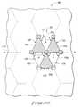
- FIG. 19a diagrammatic semiconductor mask layout and DRAM array is designated generally by reference numeral 88 .
- Layout 88is utilized to enable the above-described containers to be selectively, alternately formed or etched in the two described separate etching steps.
- FIG. 15is taken along line 15 — 15 in FIG. 19 at a processing point just after the etching of openings 76 (FIG. 15) using layout 88 .
- Layout 88enables capacitors having unique, space-saving geometries to be formed over the substrate.
- the electrically insulative partitions 74(FIG. 15) are formed between adjacent capacitors intermediate the two etching steps which form or define the areas over the substrate in which the capacitors will be formed. The partitions 74 are not shown for clarity in FIG. 19 .
- Mask layout 88includes a plurality of rows such as those illustrated at R 1 , R 2 , R 3 and R 4 .
- the mask layoutalso includes a plurality of columns such as those illustrated at C 1 , C 2 , C 3 , C 4 , C 5 , C 6 and C 7 .
- a plurality of masked areas 90 and a plurality of adjacent unmasked areas 92are defined by the layout. Unmasked areas 92 correspond to capacitor container opening patterns 76 in FIG. 15 and masked areas 90 correspond to photoresist.
- Layout 88enables a plurality of capacitors to be formed, which may be as part of a DRAM array over the substrate, wherein respective alternate capacitors in a row, such as rows R 1 -R 4 , have substantially similar lateral width profiles transverse the row.
- respective adjacent capacitors in a rowhave different lateral width profiles transverse the row.
- the illustrated lateral width profileswhen viewed from a point above the substrate approximate triangles which are oriented in a top-to-bottom fashion across the row.
- individual defined areas in which the capacitor pairs are to be formed(corresponding to the view taken along line 15 — 15 in column C 5 ) approximate a diamond shape with such shape having at its respective corners, bit line contacts 94 which are formed as described above.
- each of columns C 1 -C 7are formed along a generally straight line which is generally transverse each of rows R 1 -R 4 .
- the array of capacitor pairs to be formedare formed along individual lines which contain at least one of the pairs of capacitors.
- the arrayis defined by a plurality of the lines (corresponding to the plurality of the columns) which contain a plurality of capacitors which are separated by substantially no more than an electrically insulative anisotropically etched spacer 74 as described above.
- Underlying word linesare shown by dashed lines 93 and interconnect associated transistors formed relative to the substrate. Individual bit lines are not specifically shown but are subsequently formed and oriented generally transversely relative to the word lines 93 .
- a first of these effectsis that the wet clean following the dry etch used to form the dry etched containers may also enlarge the first capacitor containers 76 , in part by tending to make the first capacitor containers 76 more rounded. This tends to cause the first capacitor containers 76 to be enlarged relative to the second capacitor containers 78 .
- the first effecttends to be exacerbated by need to wet etch to remove any remaining BPSG from sides of the bit line contacts 72 .
- a second of these effectsis that, especially for very small first and second capacitor containers 76 and 78 , exposure of positive photoresist tends to result in curvature or rounding of edges of the photoresist patterns 90 , which also tends to enlarge the first capacitor containers 76 relative to the second capacitor containers 78 .
- a mask layout 88defines in part a DRAM array which includes a plurality of six-capacitor geometries which are to be formed over the substrate.
- a representative of one of the geometriesis indicated generally by reference numeral 96 and a plurality of adjacent or other geometries are shown in phantom lines.
- the illustrated six-capacitor geometriesare, in turn, defined by a plurality of individual polygonal capacitor geometries shown collectively at 98 through 108 .
- collective individual capacitor geometries 98 through 108approximate a hexagon, individual sides of which are defined by a side of a different respective one of the individual polygonal capacitor geometries.
- the six-capacitor geometry or hexagon 96includes six sides collectively shown at 96 a , 96 b , 96 c , 96 d , 96 e and 96 f . Each of such sides is defined by a different respective one of the individual sides of the individual polygonal capacitor geometries 98 through 108 .
- the individual polygonal capacitor geometries 98 through 108when viewed outwardly of the substrate, approximate a wedge or wedge-shape. In one embodiment, such individual geometries approximate a triangle which may be an isosceles triangle.
- individual approximated isosceles trianglesinclude equal adjacent angles ⁇ which approximate a range of between about 50° to 70°. Such equal adjacent angles are shown for the individual geometries 100 , 104 and 108 . In one embodiment, such equal adjacent angles approximate an angle of about 65°.
- the individual geometries 98 through 102 and 104 through 108may be arranged in a top-to-bottom orientation such that the hexagon 96 can be bisected, as shown by dashed line 110 , into halves containing exactly three individual polygonal capacitor geometries. In the illustrated hexagon, one of the halves, a top half as viewed in FIG. 20, contains the individual geometries 98 , 100 and 102 . The other of the halves, a bottom half, contains the geometries 104 , 106 and 108 .
- the top half containing the geometries 98 , 100 and 102is shown, comprising a three-capacitor geometry 112 .
- a plurality of three-capacitor geometries 112are disposed over the substrate.
- the three-capacitor geometry 112when viewed outwardly of the substrate, defines a pair of overlapping approximated parallelograms, the intersection of which approximates a triangle.
- a first of such parallelogramsis shown at 114 .
- a second of such parallelogramsis shown at 116 .
- the parallelogram 114includes sides 114 a , 114 b , 114 c and 114 d .
- the parallelogram 116includes sides 116 a , 116 b , 116 c and 116 d .
- the parallelogramsshare sides 114 b and 116 d .
- each approximated parallelogramis bounded at a respective one of its corners by a bit line contact 94 .
- the approximated triangle defined by the intersection of the parallelograms 114 , 116includes sides 114 c , 116 c and shared sides 114 b / 116 d .
- a plurality of capacitor pairsare selectively and alternately etched over the substrate along etch axes which are generally orthogonal relative to the substrate and into the plane of the page upon which FIG. 21 appears. Such capacitor pairs can approximate the above described parallelogram and would include the individual capacitors etched as a result of individual geometries 98 , 100 , or alternatively 100 , 102 .
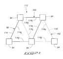
- a DRAM arrayis formed atop a substrate and includes a first set of capacitors formed in first set of capacitor containers 76 over the substrate.
- a second set of capacitorsare formed over the substrate and in second set capacitor containers 78 .
- Individual capacitors of the first setare bounded by at least three capacitors from the second set (FIG. 19 ).
- individual first set capacitorshave a closest separation distance from at least one of the three bounding capacitors which is substantially no more than a width of an electrically insulative anisotropically etched spacer 74 (FIG. 16 ).
- individual bounded first set capacitorshave closest separation distances from no less than two and possibly three of the bounding capacitors which are no more than the width of an electrically insulative anisotropically etched spacer formed or provided between the respective capacitors.
- the above described semiconductor device forming methods and integrated circuitry formed therebyconstitute an improvement which relates to device spacing over a substrate.
- Such improvementenables device pitch to be reduced by almost fifty percent or more which represents a substantial space savings over heretofore available methods and devices.
Landscapes
- Engineering & Computer Science (AREA)
- Manufacturing & Machinery (AREA)
- Physics & Mathematics (AREA)
- Condensed Matter Physics & Semiconductors (AREA)
- General Physics & Mathematics (AREA)
- Computer Hardware Design (AREA)
- Microelectronics & Electronic Packaging (AREA)
- Power Engineering (AREA)
- Semiconductor Memories (AREA)
- Internal Circuitry In Semiconductor Integrated Circuit Devices (AREA)
Abstract
Description
Claims (33)
Priority Applications (6)
| Application Number | Priority Date | Filing Date | Title |
|---|---|---|---|
| US09/651,816US6395613B1 (en) | 2000-08-30 | 2000-08-30 | Semiconductor processing methods of forming a plurality of capacitors on a substrate, bit line contacts and method of forming bit line contacts |
| US10/016,538US6635917B2 (en) | 1996-11-01 | 2001-12-12 | Semiconductor processing methods of forming a plurality of capacitors on a substrate, bit line contacts and method of forming bit line contacts |
| US10/121,538US6593203B2 (en) | 1996-11-01 | 2002-04-10 | Semiconductor processing methods of forming a plurality of capacitors on a substrate, bit line contacts and method of forming bit line contacts |
| US10/289,723US6746917B2 (en) | 1996-11-01 | 2002-11-06 | Semiconductor processing methods of forming a plurality of capacitors on a substrate, bit line contacts and method of forming bit line contacts |
| US10/734,438US6936899B2 (en) | 1996-11-01 | 2003-12-11 | Bit line contacts |
| US11/179,229US20050263794A1 (en) | 1996-11-01 | 2005-07-11 | Integrated circuitry |
Applications Claiming Priority (1)
| Application Number | Priority Date | Filing Date | Title |
|---|---|---|---|
| US09/651,816US6395613B1 (en) | 2000-08-30 | 2000-08-30 | Semiconductor processing methods of forming a plurality of capacitors on a substrate, bit line contacts and method of forming bit line contacts |
Related Parent Applications (1)
| Application Number | Title | Priority Date | Filing Date |
|---|---|---|---|
| US09/036,701Continuation-In-PartUS6482731B1 (en) | 1996-11-01 | 1998-03-06 | Semiconductor processing methods of forming devices on a substrate, forming device arrays on a substrate, forming conductive lines on a substrate, and forming capacitor arrays on a substrate, and integrated circuitry |
Related Child Applications (3)
| Application Number | Title | Priority Date | Filing Date |
|---|---|---|---|
| US10/016,538DivisionUS6635917B2 (en) | 1996-11-01 | 2001-12-12 | Semiconductor processing methods of forming a plurality of capacitors on a substrate, bit line contacts and method of forming bit line contacts |
| US10/016,538ContinuationUS6635917B2 (en) | 1996-11-01 | 2001-12-12 | Semiconductor processing methods of forming a plurality of capacitors on a substrate, bit line contacts and method of forming bit line contacts |
| US10/121,538ContinuationUS6593203B2 (en) | 1996-11-01 | 2002-04-10 | Semiconductor processing methods of forming a plurality of capacitors on a substrate, bit line contacts and method of forming bit line contacts |
Publications (1)
| Publication Number | Publication Date |
|---|---|
| US6395613B1true US6395613B1 (en) | 2002-05-28 |
Family
ID=24614336
Family Applications (6)
| Application Number | Title | Priority Date | Filing Date |
|---|---|---|---|
| US09/651,816Expired - LifetimeUS6395613B1 (en) | 1996-11-01 | 2000-08-30 | Semiconductor processing methods of forming a plurality of capacitors on a substrate, bit line contacts and method of forming bit line contacts |
| US10/016,538Expired - LifetimeUS6635917B2 (en) | 1996-11-01 | 2001-12-12 | Semiconductor processing methods of forming a plurality of capacitors on a substrate, bit line contacts and method of forming bit line contacts |
| US10/121,538Expired - Fee RelatedUS6593203B2 (en) | 1996-11-01 | 2002-04-10 | Semiconductor processing methods of forming a plurality of capacitors on a substrate, bit line contacts and method of forming bit line contacts |
| US10/289,723Expired - Fee RelatedUS6746917B2 (en) | 1996-11-01 | 2002-11-06 | Semiconductor processing methods of forming a plurality of capacitors on a substrate, bit line contacts and method of forming bit line contacts |
| US10/734,438Expired - Fee RelatedUS6936899B2 (en) | 1996-11-01 | 2003-12-11 | Bit line contacts |
| US11/179,229AbandonedUS20050263794A1 (en) | 1996-11-01 | 2005-07-11 | Integrated circuitry |
Family Applications After (5)
| Application Number | Title | Priority Date | Filing Date |
|---|---|---|---|
| US10/016,538Expired - LifetimeUS6635917B2 (en) | 1996-11-01 | 2001-12-12 | Semiconductor processing methods of forming a plurality of capacitors on a substrate, bit line contacts and method of forming bit line contacts |
| US10/121,538Expired - Fee RelatedUS6593203B2 (en) | 1996-11-01 | 2002-04-10 | Semiconductor processing methods of forming a plurality of capacitors on a substrate, bit line contacts and method of forming bit line contacts |
| US10/289,723Expired - Fee RelatedUS6746917B2 (en) | 1996-11-01 | 2002-11-06 | Semiconductor processing methods of forming a plurality of capacitors on a substrate, bit line contacts and method of forming bit line contacts |
| US10/734,438Expired - Fee RelatedUS6936899B2 (en) | 1996-11-01 | 2003-12-11 | Bit line contacts |
| US11/179,229AbandonedUS20050263794A1 (en) | 1996-11-01 | 2005-07-11 | Integrated circuitry |
Country Status (1)
| Country | Link |
|---|---|
| US (6) | US6395613B1 (en) |
Cited By (52)
| Publication number | Priority date | Publication date | Assignee | Title |
|---|---|---|---|---|
| US20030064557A1 (en)* | 1996-11-01 | 2003-04-03 | Werner Juengling | Semiconductor processing methods of forming a plurality of capacitors on a substrate, bit line contacts and method of forming bit line contacts |
| US20040076068A1 (en)* | 2001-03-08 | 2004-04-22 | Satoru Yamada | Method of producing semiconductor integrated circuit device and semiconductor integrated circuit device |
| US20060046200A1 (en)* | 2004-09-01 | 2006-03-02 | Abatchev Mirzafer K | Mask material conversion |
| US20060046201A1 (en)* | 2004-09-02 | 2006-03-02 | Sandhu Gurtej S | Method to align mask patterns |
| US20060216922A1 (en)* | 2005-03-28 | 2006-09-28 | Tran Luan C | Integrated circuit fabrication |
| US20060228854A1 (en)* | 2004-08-31 | 2006-10-12 | Luan Tran | Methods for increasing photo alignment margins |
| US20060258162A1 (en)* | 2004-09-02 | 2006-11-16 | Abatchev Mirzafer K | Method for integrated circuit fabrication using pitch multiplication |
| US20060273456A1 (en)* | 2005-06-02 | 2006-12-07 | Micron Technology, Inc., A Corporation | Multiple spacer steps for pitch multiplication |
| US20060281266A1 (en)* | 2005-06-09 | 2006-12-14 | Wells David H | Method and apparatus for adjusting feature size and position |
| US20070026672A1 (en)* | 2005-07-29 | 2007-02-01 | Micron Technology, Inc. | Pitch doubled circuit layout |
| US20070049030A1 (en)* | 2005-09-01 | 2007-03-01 | Sandhu Gurtej S | Pitch multiplication spacers and methods of forming the same |
| US20070050748A1 (en)* | 2005-08-30 | 2007-03-01 | Micron Technology, Inc., A Corporation | Method and algorithm for random half pitched interconnect layout with constant spacing |
| US20070049040A1 (en)* | 2005-03-15 | 2007-03-01 | Micron Technology, Inc., A Corporation | Multiple deposition for integration of spacers in pitch multiplication process |
| US20070049011A1 (en)* | 2005-09-01 | 2007-03-01 | Micron Technology, Inc., A Corporation | Method of forming isolated features using pitch multiplication |
| US20070049035A1 (en)* | 2005-08-31 | 2007-03-01 | Tran Luan C | Method of forming pitch multipled contacts |
| US20070044361A1 (en)* | 2005-08-31 | 2007-03-01 | Southern Imperial, Inc. | Shelf edge sign holder |
| US20070045712A1 (en)* | 2005-09-01 | 2007-03-01 | Haller Gordon A | Memory cell layout and process flow |
| US20070128856A1 (en)* | 2005-03-15 | 2007-06-07 | Micron Technology, Inc. | Pitch reduced patterns relative to photolithography features |
| US20070205438A1 (en)* | 2006-03-02 | 2007-09-06 | Werner Juengling | Masking process for simultaneously patterning separate regions |
| US20070238308A1 (en)* | 2006-04-07 | 2007-10-11 | Ardavan Niroomand | Simplified pitch doubling process flow |
| US20070249170A1 (en)* | 2006-04-25 | 2007-10-25 | David Kewley | Process for improving critical dimension uniformity of integrated circuit arrays |
| US20070261016A1 (en)* | 2006-04-24 | 2007-11-08 | Sandhu Gurtej S | Masking techniques and templates for dense semiconductor fabrication |
| US20080057692A1 (en)* | 2006-08-30 | 2008-03-06 | Wells David H | Single spacer process for multiplying pitch by a factor greater than two and related intermediate IC structures |
| US20080070165A1 (en)* | 2006-09-14 | 2008-03-20 | Mark Fischer | Efficient pitch multiplication process |
| US20080149593A1 (en)* | 2005-08-25 | 2008-06-26 | Micron Technology, Inc. | Multiple deposition for integration of spacers in pitch multiplication process |
| US7393789B2 (en) | 2005-09-01 | 2008-07-01 | Micron Technology, Inc. | Protective coating for planarization |
| US7429536B2 (en) | 2005-05-23 | 2008-09-30 | Micron Technology, Inc. | Methods for forming arrays of small, closely spaced features |
| US20080268646A1 (en)* | 2005-10-14 | 2008-10-30 | Promos Technologies Pet.Ltd. | Reduced area dynamic random access memory (dram) cell and method for fabricating the same |
| US20080299774A1 (en)* | 2007-06-04 | 2008-12-04 | Micron Technology, Inc. | Pitch multiplication using self-assembling materials |
| US20090035665A1 (en)* | 2007-07-31 | 2009-02-05 | Micron Technology, Inc. | Process of semiconductor fabrication with mask overlay on pitch multiplied features and associated structures |
| US20090152645A1 (en)* | 2007-12-18 | 2009-06-18 | Micron Technology, Inc. | Methods for isolating portions of a loop of pitch-multiplied material and related structures |
| US7566620B2 (en) | 2005-07-25 | 2009-07-28 | Micron Technology, Inc. | DRAM including a vertical surround gate transistor |
| US7572572B2 (en) | 2005-09-01 | 2009-08-11 | Micron Technology, Inc. | Methods for forming arrays of small, closely spaced features |
| US20090239366A1 (en)* | 2005-09-01 | 2009-09-24 | Hasan Nejad | Method Of Forming A Transistor Gate Of A Recessed Access Device, Method Of Forming A Recessed Transistor Gate And A Non-Recessed Transistor Gate, And Method Of Fabricating An Integrated Circuit |
| US7601595B2 (en) | 2005-07-06 | 2009-10-13 | Micron Technology, Inc. | Surround gate access transistors with grown ultra-thin bodies |
| US20100009512A1 (en)* | 2008-07-09 | 2010-01-14 | Fred Fishburn | Methods of forming a plurality of capacitors |
| US7659208B2 (en) | 2007-12-06 | 2010-02-09 | Micron Technology, Inc | Method for forming high density patterns |
| US7696567B2 (en) | 2005-08-31 | 2010-04-13 | Micron Technology, Inc | Semiconductor memory device |
| US20100130016A1 (en)* | 2008-11-24 | 2010-05-27 | Micron Technology, Inc. | Methods of forming a masking pattern for integrated circuits |
| US7737039B2 (en) | 2007-11-01 | 2010-06-15 | Micron Technology, Inc. | Spacer process for on pitch contacts and related structures |
| US7795149B2 (en) | 2006-06-01 | 2010-09-14 | Micron Technology, Inc. | Masking techniques and contact imprint reticles for dense semiconductor fabrication |
| US20110003469A1 (en)* | 2009-07-02 | 2011-01-06 | Kewley David A | Methods Of Forming Memory Cells; And Methods Of Forming Vertical Structures |
| US7939409B2 (en) | 2005-09-01 | 2011-05-10 | Micron Technology, Inc. | Peripheral gate stacks and recessed array gates |
| US8030218B2 (en) | 2008-03-21 | 2011-10-04 | Micron Technology, Inc. | Method for selectively modifying spacing between pitch multiplied structures |
| US8076208B2 (en) | 2008-07-03 | 2011-12-13 | Micron Technology, Inc. | Method for forming transistor with high breakdown voltage using pitch multiplication technique |
| US8101497B2 (en) | 2008-09-11 | 2012-01-24 | Micron Technology, Inc. | Self-aligned trench formation |
| US8101992B2 (en) | 2005-05-13 | 2012-01-24 | Micron Technology, Inc. | Memory array with surrounding gate access transistors and capacitors with global and staggered local bit lines |
| US8114573B2 (en) | 2006-06-02 | 2012-02-14 | Micron Technology, Inc. | Topography based patterning |
| US8129289B2 (en) | 2006-10-05 | 2012-03-06 | Micron Technology, Inc. | Method to deposit conformal low temperature SiO2 |
| US8227305B2 (en) | 2005-05-13 | 2012-07-24 | Micron Technology, Inc. | Memory array with ultra-thin etched pillar surround gate access transistors and buried data/bit lines |
| US8592898B2 (en) | 2006-03-02 | 2013-11-26 | Micron Technology, Inc. | Vertical gated access transistor |
| US9076680B2 (en) | 2011-10-18 | 2015-07-07 | Micron Technology, Inc. | Integrated circuitry, methods of forming capacitors, and methods of forming integrated circuitry comprising an array of capacitors and circuitry peripheral to the array |
Families Citing this family (15)
| Publication number | Priority date | Publication date | Assignee | Title |
|---|---|---|---|---|
| DE102004010379A1 (en)* | 2004-03-03 | 2005-09-22 | Schott Ag | Process for the production of wafers with low-defect surfaces, the use of such wafers and electronic components obtained therefrom |
| US7468306B2 (en)* | 2005-05-31 | 2008-12-23 | Qimonds Ag | Method of manufacturing a semiconductor device |
| US7897058B2 (en)* | 2006-02-13 | 2011-03-01 | Asml Netherlands B.V. | Device manufacturing method and computer program product |
| US20080113483A1 (en)* | 2006-11-15 | 2008-05-15 | Micron Technology, Inc. | Methods of etching a pattern layer to form staggered heights therein and intermediate semiconductor device structures |
| US8211806B2 (en)* | 2007-08-29 | 2012-07-03 | Macronix International Co., Ltd. | Method of fabricating integrated circuit with small pitch |
| US7800965B2 (en) | 2008-03-10 | 2010-09-21 | Micron Technology, Inc. | Digit line equilibration using access devices at the edge of sub-arrays |
| JP2009239030A (en)* | 2008-03-27 | 2009-10-15 | Toshiba Corp | Method of manufacturing semiconductor device |
| US12179028B2 (en) | 2009-07-31 | 2024-12-31 | Medtronic, Inc. | Implantable medical device |
| US10449373B2 (en) | 2009-07-31 | 2019-10-22 | Medtronic, Inc. | Connector enclosure assemblies of medical devices including an angled lead passageway |
| US9144689B2 (en) | 2010-12-28 | 2015-09-29 | Medtronic, Inc. | Medical devices including metallic connector enclosures |
| EP2667936B1 (en) | 2011-01-26 | 2017-08-23 | Medtronic, Inc. | Implantable medical devices and related connector enclosure assemblies utilizing conductors electrically coupled to feedthrough pins |
| US8593816B2 (en) | 2011-09-21 | 2013-11-26 | Medtronic, Inc. | Compact connector assembly for implantable medical device |
| US8735296B2 (en)* | 2012-07-18 | 2014-05-27 | International Business Machines Corporation | Method of simultaneously forming multiple structures having different critical dimensions using sidewall transfer |
| US11253708B2 (en) | 2018-05-24 | 2022-02-22 | Medtronic, Inc. | Machined features of enclosures for implantable medical devices |
| CN112542385B (en)* | 2019-09-20 | 2024-11-22 | 中芯国际集成电路制造(上海)有限公司 | Semiconductor structure and method for forming the same |
Citations (6)
| Publication number | Priority date | Publication date | Assignee | Title |
|---|---|---|---|---|
| US4999689A (en)* | 1987-11-06 | 1991-03-12 | Sharp Kabushiki Kaisha | Semiconductor memory |
| US5496757A (en)* | 1992-07-08 | 1996-03-05 | Siemens Aktiengesellschaft | Process for producing storage capacitors for DRAM cells |
| US5554557A (en)* | 1996-02-02 | 1996-09-10 | Vanguard International Semiconductor Corp. | Method for fabricating a stacked capacitor with a self aligned node contact in a memory cell |
| US5792687A (en)* | 1996-08-01 | 1998-08-11 | Vanguard International Semiconductor Corporation | Method for fabricating high density integrated circuits using oxide and polysilicon spacers |
| US5998256A (en)* | 1996-11-01 | 1999-12-07 | Micron Technology, Inc. | Semiconductor processing methods of forming devices on a substrate, forming device arrays on a substrate, forming conductive lines on a substrate, and forming capacitor arrays on a substrate, and integrated circuitry |
| US6160283A (en)* | 1998-01-29 | 2000-12-12 | Micron Technology, Inc. | Methods of forming integrated circuitry and integrated circuitry structures |
Family Cites Families (12)
| Publication number | Priority date | Publication date | Assignee | Title |
|---|---|---|---|---|
| KR940006682B1 (en)* | 1991-10-17 | 1994-07-25 | 삼성전자 주식회사 | Manufacturing Method of Semiconductor Memory Device |
| US5206183A (en)* | 1992-02-19 | 1993-04-27 | Micron Technology, Inc. | Method of forming a bit line over capacitor array of memory cells |
| US5250457A (en)* | 1992-02-19 | 1993-10-05 | Micron Technology, Inc. | Method of forming a buried bit line array of memory cells |
| KR100260577B1 (en)* | 1992-09-09 | 2000-08-01 | 김영환 | Method of making a self-aligned contact in semiconductor device |
| US5605857A (en)* | 1993-02-12 | 1997-02-25 | Micron Technology, Inc. | Method of forming a bit line over capacitor array of memory cells and an array of bit line over capacitor array of memory cells |
| US5956615A (en)* | 1994-05-31 | 1999-09-21 | Stmicroelectronics, Inc. | Method of forming a metal contact to landing pad structure in an integrated circuit |
| US5851872A (en)* | 1996-04-03 | 1998-12-22 | United Microelectronics Corporation | Method of fabricating dynamic random access memory |
| US5705438A (en)* | 1996-10-18 | 1998-01-06 | Vanguard International Semiconductor Corporation | Method for manufacturing stacked dynamic random access memories using reduced photoresist masking steps |
| US6395613B1 (en)* | 2000-08-30 | 2002-05-28 | Micron Technology, Inc. | Semiconductor processing methods of forming a plurality of capacitors on a substrate, bit line contacts and method of forming bit line contacts |
| US5702972A (en)* | 1997-01-27 | 1997-12-30 | Taiwan Semiconductor Manufacturing Company Ltd. | Method of fabricating MOSFET devices |
| US5998257A (en) | 1997-03-13 | 1999-12-07 | Micron Technology, Inc. | Semiconductor processing methods of forming integrated circuitry memory devices, methods of forming capacitor containers, methods of making electrical connection to circuit nodes and related integrated circuitry |
| US6194302B1 (en)* | 1999-09-30 | 2001-02-27 | Taiwan Semiconductor Manufacturing Company | Integrated process flow to improve the electrical isolation within self aligned contact structure |
- 2000
- 2000-08-30USUS09/651,816patent/US6395613B1/ennot_activeExpired - Lifetime
- 2001
- 2001-12-12USUS10/016,538patent/US6635917B2/ennot_activeExpired - Lifetime
- 2002
- 2002-04-10USUS10/121,538patent/US6593203B2/ennot_activeExpired - Fee Related
- 2002-11-06USUS10/289,723patent/US6746917B2/ennot_activeExpired - Fee Related
- 2003
- 2003-12-11USUS10/734,438patent/US6936899B2/ennot_activeExpired - Fee Related
- 2005
- 2005-07-11USUS11/179,229patent/US20050263794A1/ennot_activeAbandoned
Patent Citations (6)
| Publication number | Priority date | Publication date | Assignee | Title |
|---|---|---|---|---|
| US4999689A (en)* | 1987-11-06 | 1991-03-12 | Sharp Kabushiki Kaisha | Semiconductor memory |
| US5496757A (en)* | 1992-07-08 | 1996-03-05 | Siemens Aktiengesellschaft | Process for producing storage capacitors for DRAM cells |
| US5554557A (en)* | 1996-02-02 | 1996-09-10 | Vanguard International Semiconductor Corp. | Method for fabricating a stacked capacitor with a self aligned node contact in a memory cell |
| US5792687A (en)* | 1996-08-01 | 1998-08-11 | Vanguard International Semiconductor Corporation | Method for fabricating high density integrated circuits using oxide and polysilicon spacers |
| US5998256A (en)* | 1996-11-01 | 1999-12-07 | Micron Technology, Inc. | Semiconductor processing methods of forming devices on a substrate, forming device arrays on a substrate, forming conductive lines on a substrate, and forming capacitor arrays on a substrate, and integrated circuitry |
| US6160283A (en)* | 1998-01-29 | 2000-12-12 | Micron Technology, Inc. | Methods of forming integrated circuitry and integrated circuitry structures |
Cited By (221)
| Publication number | Priority date | Publication date | Assignee | Title |
|---|---|---|---|---|
| US20030064557A1 (en)* | 1996-11-01 | 2003-04-03 | Werner Juengling | Semiconductor processing methods of forming a plurality of capacitors on a substrate, bit line contacts and method of forming bit line contacts |
| US6593203B2 (en)* | 1996-11-01 | 2003-07-15 | Micron Technology, Inc. | Semiconductor processing methods of forming a plurality of capacitors on a substrate, bit line contacts and method of forming bit line contacts |
| US6635917B2 (en) | 1996-11-01 | 2003-10-21 | Micron Technology, Inc. | Semiconductor processing methods of forming a plurality of capacitors on a substrate, bit line contacts and method of forming bit line contacts |
| US6746917B2 (en)* | 1996-11-01 | 2004-06-08 | Micron Technology, Inc. | Semiconductor processing methods of forming a plurality of capacitors on a substrate, bit line contacts and method of forming bit line contacts |
| US20040127018A1 (en)* | 1996-11-01 | 2004-07-01 | Werner Juengling | Bit line contacts |
| US6936899B2 (en) | 1996-11-01 | 2005-08-30 | Micron Technology, Inc. | Bit line contacts |
| US20040076068A1 (en)* | 2001-03-08 | 2004-04-22 | Satoru Yamada | Method of producing semiconductor integrated circuit device and semiconductor integrated circuit device |
| US7141471B2 (en)* | 2001-03-08 | 2006-11-28 | Elpida Memory, Inc. | Method of producing semiconductor integrated circuit device and semiconductor integrated circuit device |
| US20060228854A1 (en)* | 2004-08-31 | 2006-10-12 | Luan Tran | Methods for increasing photo alignment margins |
| US7268054B2 (en) | 2004-08-31 | 2007-09-11 | Micron Technology, Inc. | Methods for increasing photo-alignment margins |
| US8030222B2 (en) | 2004-08-31 | 2011-10-04 | Round Rock Research, Llc | Structures with increased photo-alignment margins |
| US7361569B2 (en) | 2004-08-31 | 2008-04-22 | Micron Technology, Inc. | Methods for increasing photo-alignment margins |
| US20060264001A1 (en)* | 2004-08-31 | 2006-11-23 | Luan Tran | Structures with increased photo-alignment margins |
| US20060264000A1 (en)* | 2004-08-31 | 2006-11-23 | Luan Tran | Methods for increasing photo-alignment margins |
| US7368362B2 (en) | 2004-08-31 | 2008-05-06 | Micron Technology, Inc. | Methods for increasing photo alignment margins |
| US20060264002A1 (en)* | 2004-08-31 | 2006-11-23 | Luan Tran | Methods for increasing photo-alignment margins |
| US8486610B2 (en) | 2004-09-01 | 2013-07-16 | Micron Technology, Inc. | Mask material conversion |
| US20060046200A1 (en)* | 2004-09-01 | 2006-03-02 | Abatchev Mirzafer K | Mask material conversion |
| US7910288B2 (en) | 2004-09-01 | 2011-03-22 | Micron Technology, Inc. | Mask material conversion |
| US8895232B2 (en) | 2004-09-01 | 2014-11-25 | Micron Technology, Inc. | Mask material conversion |
| US20100203727A1 (en)* | 2004-09-02 | 2010-08-12 | Micron Technology, Inc. | Method for integrated circuit fabrication using pitch multiplication |
| US20100092890A1 (en)* | 2004-09-02 | 2010-04-15 | Micron Technology, Inc. | Method to align mask patterns |
| US7687408B2 (en) | 2004-09-02 | 2010-03-30 | Micron Technology, Inc. | Method for integrated circuit fabrication using pitch multiplication |
| US8216949B2 (en) | 2004-09-02 | 2012-07-10 | Round Rock Research, Llc | Method for integrated circuit fabrication using pitch multiplication |
| US8338085B2 (en) | 2004-09-02 | 2012-12-25 | Micron Technology, Inc. | Method to align mask patterns |
| US7455956B2 (en) | 2004-09-02 | 2008-11-25 | Micron Technology, Inc. | Method to align mask patterns |
| US7629693B2 (en) | 2004-09-02 | 2009-12-08 | Micron Technology, Inc | Method for integrated circuit fabrication using pitch multiplication |
| US7655387B2 (en) | 2004-09-02 | 2010-02-02 | Micron Technology, Inc. | Method to align mask patterns |
| US7547640B2 (en) | 2004-09-02 | 2009-06-16 | Micron Technology, Inc. | Method for integrated circuit fabrication using pitch multiplication |
| US20060262511A1 (en)* | 2004-09-02 | 2006-11-23 | Abatchev Mirzafer K | Method for integrated circuit fabrication using pitch multiplication |
| US20060258162A1 (en)* | 2004-09-02 | 2006-11-16 | Abatchev Mirzafer K | Method for integrated circuit fabrication using pitch multiplication |
| US20070190463A1 (en)* | 2004-09-02 | 2007-08-16 | Micron Technology, Inc. | Method to align mask patterns |
| US20060240362A1 (en)* | 2004-09-02 | 2006-10-26 | Sandhu Gurtej S | Method to align mask patterns |
| US7435536B2 (en) | 2004-09-02 | 2008-10-14 | Micron Technology, Inc. | Method to align mask patterns |
| US8674512B2 (en) | 2004-09-02 | 2014-03-18 | Micron Technology, Inc. | Method to align mask patterns |
| US20060046201A1 (en)* | 2004-09-02 | 2006-03-02 | Sandhu Gurtej S | Method to align mask patterns |
| US20070049040A1 (en)* | 2005-03-15 | 2007-03-01 | Micron Technology, Inc., A Corporation | Multiple deposition for integration of spacers in pitch multiplication process |
| US8598632B2 (en) | 2005-03-15 | 2013-12-03 | Round Rock Research Llc | Integrated circuit having pitch reduced patterns relative to photoithography features |
| US20110117743A1 (en)* | 2005-03-15 | 2011-05-19 | Round Rock Research, Llc | Multiple deposition for integration of spacers in pitch multiplication process |
| US8048812B2 (en) | 2005-03-15 | 2011-11-01 | Round Rock Research, Llc | Pitch reduced patterns relative to photolithography features |
| US7651951B2 (en) | 2005-03-15 | 2010-01-26 | Micron Technology, Inc. | Pitch reduced patterns relative to photolithography features |
| US20070161251A1 (en)* | 2005-03-15 | 2007-07-12 | Micron Technology, Inc. | Pitch reduced patterns relative to photolithography features |
| US20070138526A1 (en)* | 2005-03-15 | 2007-06-21 | Micron Technology, Inc. | Pitch reduced patterns relative to photolithography features |
| US7390746B2 (en) | 2005-03-15 | 2008-06-24 | Micron Technology, Inc. | Multiple deposition for integration of spacers in pitch multiplication process |
| US20070128856A1 (en)* | 2005-03-15 | 2007-06-07 | Micron Technology, Inc. | Pitch reduced patterns relative to photolithography features |
| US7884022B2 (en) | 2005-03-15 | 2011-02-08 | Round Rock Research, Llc | Multiple deposition for integration of spacers in pitch multiplication process |
| US8119535B2 (en) | 2005-03-15 | 2012-02-21 | Round Rock Research, Llc | Pitch reduced patterns relative to photolithography features |
| US8207576B2 (en) | 2005-03-15 | 2012-06-26 | Round Rock Research, Llc | Pitch reduced patterns relative to photolithography features |
| US20100210111A1 (en)* | 2005-03-15 | 2010-08-19 | Round Rock Research, Llc | Pitch reduced patterns relative tophotolithography features |
| US20100092891A1 (en)* | 2005-03-15 | 2010-04-15 | Micron Technology, Inc. | Pitch reduced patterns relative to photolithography features |
| US7718540B2 (en) | 2005-03-15 | 2010-05-18 | Round Rock Research, Llc | Pitch reduced patterns relative to photolithography features |
| US9147608B2 (en) | 2005-03-28 | 2015-09-29 | Micron Technology, Inc. | Integrated circuit fabrication |
| US7776683B2 (en) | 2005-03-28 | 2010-08-17 | Micron Technology, Inc. | Integrated circuit fabrication |
| US7648919B2 (en) | 2005-03-28 | 2010-01-19 | Tran Luan C | Integrated circuit fabrication |
| US8507341B2 (en) | 2005-03-28 | 2013-08-13 | Micron Technology, Inc. | Integrated circuit fabrication |
| US20080227293A1 (en)* | 2005-03-28 | 2008-09-18 | Micron Technology, Inc. | Integrated circuit fabrication |
| US8859362B2 (en) | 2005-03-28 | 2014-10-14 | Micron Technology, Inc. | Integrated circuit fabrication |
| US20060216922A1 (en)* | 2005-03-28 | 2006-09-28 | Tran Luan C | Integrated circuit fabrication |
| US8158476B2 (en) | 2005-03-28 | 2012-04-17 | Micron Technology, Inc. | Integrated circuit fabrication |
| US9412594B2 (en) | 2005-03-28 | 2016-08-09 | Micron Technology, Inc. | Integrated circuit fabrication |
| US8350320B2 (en) | 2005-05-13 | 2013-01-08 | Micron Technology, Inc. | Memory array and memory device |
| US8609523B2 (en) | 2005-05-13 | 2013-12-17 | Micron Technology, Inc. | Method of making a memory array with surrounding gate access transistors and capacitors with global staggered local bit lines |
| US8227305B2 (en) | 2005-05-13 | 2012-07-24 | Micron Technology, Inc. | Memory array with ultra-thin etched pillar surround gate access transistors and buried data/bit lines |
| US8101992B2 (en) | 2005-05-13 | 2012-01-24 | Micron Technology, Inc. | Memory array with surrounding gate access transistors and capacitors with global and staggered local bit lines |
| US8637362B2 (en) | 2005-05-13 | 2014-01-28 | Micron Technology, Inc. | Memory array with ultra-thin etched pillar surround gate access transistors and buried data/bit lines |
| US9099402B2 (en) | 2005-05-23 | 2015-08-04 | Micron Technology, Inc. | Integrated circuit structure having arrays of small, closely spaced features |
| US7429536B2 (en) | 2005-05-23 | 2008-09-30 | Micron Technology, Inc. | Methods for forming arrays of small, closely spaced features |
| US8207614B2 (en) | 2005-05-23 | 2012-06-26 | Micron Technology, Inc. | Methods for forming arrays of small, closely spaced features |
| US8598041B2 (en) | 2005-06-02 | 2013-12-03 | Micron Technology, Inc. | Method for positioning spacers in pitch multiplication |
| US8173550B2 (en) | 2005-06-02 | 2012-05-08 | Micron Technology, Inc. | Method for positioning spacers for pitch multiplication |
| US20090258492A1 (en)* | 2005-06-02 | 2009-10-15 | Micron Technology, Inc. | Multiple spacer steps for pitch multiplication |
| US20060273456A1 (en)* | 2005-06-02 | 2006-12-07 | Micron Technology, Inc., A Corporation | Multiple spacer steps for pitch multiplication |
| US8865598B2 (en) | 2005-06-02 | 2014-10-21 | Micron Technology, Inc. | Method for positioning spacers in pitch multiplication |
| US8003542B2 (en) | 2005-06-02 | 2011-08-23 | Micron Technology, Inc. | Multiple spacer steps for pitch multiplication |
| US7560390B2 (en) | 2005-06-02 | 2009-07-14 | Micron Technology, Inc. | Multiple spacer steps for pitch multiplication |
| US9117766B2 (en) | 2005-06-02 | 2015-08-25 | Micron Technology, Inc. | Method for positioning spacers in pitch multiplication |
| US7396781B2 (en) | 2005-06-09 | 2008-07-08 | Micron Technology, Inc. | Method and apparatus for adjusting feature size and position |
| US20080254627A1 (en)* | 2005-06-09 | 2008-10-16 | Micron Technology, Inc. | Method for adjusting feature size and position |
| US8703616B2 (en) | 2005-06-09 | 2014-04-22 | Round Rock Research, Llc | Method for adjusting feature size and position |
| US20060281266A1 (en)* | 2005-06-09 | 2006-12-14 | Wells David H | Method and apparatus for adjusting feature size and position |
| US7888721B2 (en) | 2005-07-06 | 2011-02-15 | Micron Technology, Inc. | Surround gate access transistors with grown ultra-thin bodies |
| US8115243B2 (en) | 2005-07-06 | 2012-02-14 | Micron Technology, Inc. | Surround gate access transistors with grown ultra-thin bodies |
| US7601595B2 (en) | 2005-07-06 | 2009-10-13 | Micron Technology, Inc. | Surround gate access transistors with grown ultra-thin bodies |
| US7626219B2 (en) | 2005-07-06 | 2009-12-01 | Micron Technology, Inc. | Surround gate access transistors with grown ultra-thin bodies |
| US7768051B2 (en) | 2005-07-25 | 2010-08-03 | Micron Technology, Inc. | DRAM including a vertical surround gate transistor |
| US7566620B2 (en) | 2005-07-25 | 2009-07-28 | Micron Technology, Inc. | DRAM including a vertical surround gate transistor |
| US20080290374A1 (en)* | 2005-07-29 | 2008-11-27 | Micron Technology, Inc. | Layout for high density conductive interconnects |
| US8264010B2 (en) | 2005-07-29 | 2012-09-11 | Round Rock Research, Llc | Layout for high density conductive interconnects |
| US7413981B2 (en) | 2005-07-29 | 2008-08-19 | Micron Technology, Inc. | Pitch doubled circuit layout |
| US7767573B2 (en) | 2005-07-29 | 2010-08-03 | Round Rock Research, Llc | Layout for high density conductive interconnects |
| US20070026672A1 (en)* | 2005-07-29 | 2007-02-01 | Micron Technology, Inc. | Pitch doubled circuit layout |
| US20110006347A1 (en)* | 2005-07-29 | 2011-01-13 | Round Rock Research, Llc | Layout for high density conductive interconnects |
| US8123968B2 (en) | 2005-08-25 | 2012-02-28 | Round Rock Research, Llc | Multiple deposition for integration of spacers in pitch multiplication process |
| US20080149593A1 (en)* | 2005-08-25 | 2008-06-26 | Micron Technology, Inc. | Multiple deposition for integration of spacers in pitch multiplication process |
| US8148247B2 (en) | 2005-08-30 | 2012-04-03 | Micron Technology, Inc. | Method and algorithm for random half pitched interconnect layout with constant spacing |
| US20070050748A1 (en)* | 2005-08-30 | 2007-03-01 | Micron Technology, Inc., A Corporation | Method and algorithm for random half pitched interconnect layout with constant spacing |
| US8877639B2 (en) | 2005-08-30 | 2014-11-04 | Micron Technology, Inc. | Method and algorithm for random half pitched interconnect layout with constant spacing |
| US20110034024A1 (en)* | 2005-08-30 | 2011-02-10 | Micron Technology, Inc. | Method and algorithm for random half pitched interconnect layout with constant spacing |
| US7816262B2 (en) | 2005-08-30 | 2010-10-19 | Micron Technology, Inc. | Method and algorithm for random half pitched interconnect layout with constant spacing |
| US8546215B2 (en) | 2005-08-31 | 2013-10-01 | Micron Technology, Inc. | Methods of fabricating a memory device |
| US7696567B2 (en) | 2005-08-31 | 2010-04-13 | Micron Technology, Inc | Semiconductor memory device |
| US8426118B2 (en) | 2005-08-31 | 2013-04-23 | Micron Technology, Inc. | Method of forming pitch multiplied contacts |
| US7322138B2 (en) | 2005-08-31 | 2008-01-29 | Southern Imperial, Inc. | Shelf edge sign holder |
| US7829262B2 (en) | 2005-08-31 | 2010-11-09 | Micron Technology, Inc. | Method of forming pitch multipled contacts |
| US8609324B2 (en) | 2005-08-31 | 2013-12-17 | Micron Technology, Inc. | Method of forming pitch multiplied contacts |
| US20070044361A1 (en)* | 2005-08-31 | 2007-03-01 | Southern Imperial, Inc. | Shelf edge sign holder |
| US8481385B2 (en) | 2005-08-31 | 2013-07-09 | Micron Technology, Inc. | Methods of fabricating a memory device |
| US8222105B2 (en) | 2005-08-31 | 2012-07-17 | Micron Technology, Inc. | Methods of fabricating a memory device |
| US20110014574A1 (en)* | 2005-08-31 | 2011-01-20 | Micron Technology, Inc. | Method of forming pitch multipled contacts |
| US20070049035A1 (en)* | 2005-08-31 | 2007-03-01 | Tran Luan C | Method of forming pitch multipled contacts |
| US20100267240A1 (en)* | 2005-09-01 | 2010-10-21 | Micron Technology, Inc. | Pitch multiplication spacers and methods of forming the same |
| US8043915B2 (en) | 2005-09-01 | 2011-10-25 | Micron Technology, Inc. | Pitch multiplied mask patterns for isolated features |
| US20080261349A1 (en)* | 2005-09-01 | 2008-10-23 | Micron Technology, Inc. | Protective coating for planarization |
| US7393789B2 (en) | 2005-09-01 | 2008-07-01 | Micron Technology, Inc. | Protective coating for planarization |
| US9003651B2 (en) | 2005-09-01 | 2015-04-14 | Micron Technology, Inc. | Methods for integrated circuit fabrication with protective coating for planarization |
| US9082829B2 (en) | 2005-09-01 | 2015-07-14 | Micron Technology, Inc. | Methods for forming arrays of small, closely spaced features |
| US7935999B2 (en) | 2005-09-01 | 2011-05-03 | Micron Technology, Inc. | Memory device |
| US7939409B2 (en) | 2005-09-01 | 2011-05-10 | Micron Technology, Inc. | Peripheral gate stacks and recessed array gates |
| US9099314B2 (en) | 2005-09-01 | 2015-08-04 | Micron Technology, Inc. | Pitch multiplication spacers and methods of forming the same |
| US7776744B2 (en) | 2005-09-01 | 2010-08-17 | Micron Technology, Inc. | Pitch multiplication spacers and methods of forming the same |
| US7977236B2 (en) | 2005-09-01 | 2011-07-12 | Micron Technology, Inc. | Method of forming a transistor gate of a recessed access device, method of forming a recessed transistor gate and a non-recessed transistor gate, and method of fabricating an integrated circuit |
| US9076888B2 (en) | 2005-09-01 | 2015-07-07 | Micron Technology, Inc. | Silicided recessed silicon |
| US20070045712A1 (en)* | 2005-09-01 | 2007-03-01 | Haller Gordon A | Memory cell layout and process flow |
| US8431971B2 (en) | 2005-09-01 | 2013-04-30 | Micron Technology, Inc. | Pitch multiplied mask patterns for isolated features |
| US8011090B2 (en) | 2005-09-01 | 2011-09-06 | Micron Technology, Inc. | Method for forming and planarizing adjacent regions of an integrated circuit |
| US8479384B2 (en) | 2005-09-01 | 2013-07-09 | Micron Technology, Inc. | Methods for integrated circuit fabrication with protective coating for planarization |
| US10396281B2 (en) | 2005-09-01 | 2019-08-27 | Micron Technology, Inc. | Methods for forming arrays of small, closely spaced features |
| US8266558B2 (en) | 2005-09-01 | 2012-09-11 | Micron Technology, Inc. | Methods for forming arrays of small, closely spaced features |
| US20090271758A1 (en)* | 2005-09-01 | 2009-10-29 | Micron Technology, Inc. | Methods for forming arrays of small, closely spaced features |
| US7759197B2 (en) | 2005-09-01 | 2010-07-20 | Micron Technology, Inc. | Method of forming isolated features using pitch multiplication |
| US20090239366A1 (en)* | 2005-09-01 | 2009-09-24 | Hasan Nejad | Method Of Forming A Transistor Gate Of A Recessed Access Device, Method Of Forming A Recessed Transistor Gate And A Non-Recessed Transistor Gate, And Method Of Fabricating An Integrated Circuit |
| US9679781B2 (en) | 2005-09-01 | 2017-06-13 | Micron Technology, Inc. | Methods for integrated circuit fabrication with protective coating for planarization |
| US20070049011A1 (en)* | 2005-09-01 | 2007-03-01 | Micron Technology, Inc., A Corporation | Method of forming isolated features using pitch multiplication |
| US7572572B2 (en) | 2005-09-01 | 2009-08-11 | Micron Technology, Inc. | Methods for forming arrays of small, closely spaced features |
| US8601410B2 (en) | 2005-09-01 | 2013-12-03 | Micron Technology, Inc. | Methods for forming arrays of small, closely spaced features |
| US8252646B2 (en) | 2005-09-01 | 2012-08-28 | Micron Technology, Inc. | Peripheral gate stacks and recessed array gates |
| US7687342B2 (en) | 2005-09-01 | 2010-03-30 | Micron Technology, Inc. | Method of manufacturing a memory device |
| US20100243161A1 (en)* | 2005-09-01 | 2010-09-30 | Micron Technology, Inc. | Pitch multiplied mask patterns for isolated features |
| US20070049030A1 (en)* | 2005-09-01 | 2007-03-01 | Sandhu Gurtej S | Pitch multiplication spacers and methods of forming the same |
| US20080268646A1 (en)* | 2005-10-14 | 2008-10-30 | Promos Technologies Pet.Ltd. | Reduced area dynamic random access memory (dram) cell and method for fabricating the same |
| US9184161B2 (en) | 2006-03-02 | 2015-11-10 | Micron Technology, Inc. | Vertical gated access transistor |
| US8592898B2 (en) | 2006-03-02 | 2013-11-26 | Micron Technology, Inc. | Vertical gated access transistor |
| US20070205438A1 (en)* | 2006-03-02 | 2007-09-06 | Werner Juengling | Masking process for simultaneously patterning separate regions |
| US8772840B2 (en) | 2006-03-02 | 2014-07-08 | Micron Technology, Inc. | Memory device comprising an array portion and a logic portion |
| US8207583B2 (en) | 2006-03-02 | 2012-06-26 | Micron Technology, Inc. | Memory device comprising an array portion and a logic portion |
| US7842558B2 (en) | 2006-03-02 | 2010-11-30 | Micron Technology, Inc. | Masking process for simultaneously patterning separate regions |
| US20110042755A1 (en)* | 2006-03-02 | 2011-02-24 | Micron Technology, Inc. | Memory device comprising an array portion and a logic portion |
| US7732343B2 (en) | 2006-04-07 | 2010-06-08 | Micron Technology, Inc. | Simplified pitch doubling process flow |
| US9184159B2 (en) | 2006-04-07 | 2015-11-10 | Micron Technology, Inc. | Simplified pitch doubling process flow |
| US8338959B2 (en) | 2006-04-07 | 2012-12-25 | Micron Technology, Inc. | Simplified pitch doubling process flow |
| US20070238299A1 (en)* | 2006-04-07 | 2007-10-11 | Micron Technology, Inc. | Simplified pitch doubling process flow |
| US20070238308A1 (en)* | 2006-04-07 | 2007-10-11 | Ardavan Niroomand | Simplified pitch doubling process flow |
| US8030217B2 (en) | 2006-04-07 | 2011-10-04 | Micron Technology, Inc. | Simplified pitch doubling process flow |
| US7902074B2 (en) | 2006-04-07 | 2011-03-08 | Micron Technology, Inc. | Simplified pitch doubling process flow |
| US8003310B2 (en) | 2006-04-24 | 2011-08-23 | Micron Technology, Inc. | Masking techniques and templates for dense semiconductor fabrication |
| US20070261016A1 (en)* | 2006-04-24 | 2007-11-08 | Sandhu Gurtej S | Masking techniques and templates for dense semiconductor fabrication |
| US7488685B2 (en) | 2006-04-25 | 2009-02-10 | Micron Technology, Inc. | Process for improving critical dimension uniformity of integrated circuit arrays |
| US9553082B2 (en) | 2006-04-25 | 2017-01-24 | Micron Technology, Inc. | Process for improving critical dimension uniformity of integrated circuit arrays |
| US8889020B2 (en) | 2006-04-25 | 2014-11-18 | Micron Technology, Inc. | Process for improving critical dimension uniformity of integrated circuit arrays |
| US20070249170A1 (en)* | 2006-04-25 | 2007-10-25 | David Kewley | Process for improving critical dimension uniformity of integrated circuit arrays |
| US8334211B2 (en) | 2006-04-25 | 2012-12-18 | Micron Technology, Inc. | Process for improving critical dimension uniformity of integrated circuit arrays |
| US20090130852A1 (en)* | 2006-04-25 | 2009-05-21 | Micron Technology, Inc. | Process for improving critical dimension uniformity of integrated circuit arrays |
| US8663532B2 (en) | 2006-06-01 | 2014-03-04 | Micron Technology, Inc. | Masking techniques and contact imprint reticles for dense semiconductor fabrication |
| US8449805B2 (en) | 2006-06-01 | 2013-05-28 | Micron Technology, Inc. | Masking techniques and contact imprint reticles for dense semiconductor fabrication |
| US7795149B2 (en) | 2006-06-01 | 2010-09-14 | Micron Technology, Inc. | Masking techniques and contact imprint reticles for dense semiconductor fabrication |
| US20100258966A1 (en)* | 2006-06-01 | 2010-10-14 | Micron Technology, Inc. | Masking techniques and contact imprint reticles for dense semiconductor fabrication |
| US8114573B2 (en) | 2006-06-02 | 2012-02-14 | Micron Technology, Inc. | Topography based patterning |
| US8592940B2 (en) | 2006-06-02 | 2013-11-26 | Micron Technology, Inc. | Topography based patterning |
| US20100029081A1 (en)* | 2006-08-30 | 2010-02-04 | Micron Technology, Inc. | Single spacer process for multiplying pitch by a factor greater than two and related intermediate ic structures |
| US9478497B2 (en) | 2006-08-30 | 2016-10-25 | Micron Technology, Inc. | Single spacer process for multiplying pitch by a factor greater than two and related intermediate IC structures |
| US7611980B2 (en) | 2006-08-30 | 2009-11-03 | Micron Technology, Inc. | Single spacer process for multiplying pitch by a factor greater than two and related intermediate IC structures |
| US8557704B2 (en) | 2006-08-30 | 2013-10-15 | Micron Technology, Inc. | Single spacer process for multiplying pitch by a factor greater than two and related intermediate IC structures |
| US8883644B2 (en) | 2006-08-30 | 2014-11-11 | Micron Technology, Inc. | Single spacer process for multiplying pitch by a factor greater than two and related intermediate IC structures |
| US20080057692A1 (en)* | 2006-08-30 | 2008-03-06 | Wells David H | Single spacer process for multiplying pitch by a factor greater than two and related intermediate IC structures |
| US8450829B2 (en) | 2006-09-14 | 2013-05-28 | Micron Technology, Inc. | Efficient pitch multiplication process |
| US8012674B2 (en) | 2006-09-14 | 2011-09-06 | Micron Technology, Inc. | Efficient pitch multiplication process |
| US20100112489A1 (en)* | 2006-09-14 | 2010-05-06 | Micron Technology, Inc. | Efficient pitch multiplication process |
| US20080070165A1 (en)* | 2006-09-14 | 2008-03-20 | Mark Fischer | Efficient pitch multiplication process |
| US7666578B2 (en) | 2006-09-14 | 2010-02-23 | Micron Technology, Inc. | Efficient pitch multiplication process |
| US9035416B2 (en) | 2006-09-14 | 2015-05-19 | Micron Technology, Inc. | Efficient pitch multiplication process |
| US8129289B2 (en) | 2006-10-05 | 2012-03-06 | Micron Technology, Inc. | Method to deposit conformal low temperature SiO2 |
| US20080299774A1 (en)* | 2007-06-04 | 2008-12-04 | Micron Technology, Inc. | Pitch multiplication using self-assembling materials |
| US7923373B2 (en) | 2007-06-04 | 2011-04-12 | Micron Technology, Inc. | Pitch multiplication using self-assembling materials |
| US10515801B2 (en) | 2007-06-04 | 2019-12-24 | Micron Technology, Inc. | Pitch multiplication using self-assembling materials |
| US8563229B2 (en) | 2007-07-31 | 2013-10-22 | Micron Technology, Inc. | Process of semiconductor fabrication with mask overlay on pitch multiplied features and associated structures |
| US9412591B2 (en) | 2007-07-31 | 2016-08-09 | Micron Technology, Inc. | Process of semiconductor fabrication with mask overlay on pitch multiplied features and associated structures |
| US20090035665A1 (en)* | 2007-07-31 | 2009-02-05 | Micron Technology, Inc. | Process of semiconductor fabrication with mask overlay on pitch multiplied features and associated structures |
| US7737039B2 (en) | 2007-11-01 | 2010-06-15 | Micron Technology, Inc. | Spacer process for on pitch contacts and related structures |
| US8772166B2 (en) | 2007-11-01 | 2014-07-08 | Micron Technology, Inc. | Spacer process for on pitch contacts and related structures |
| US8211803B2 (en) | 2007-11-01 | 2012-07-03 | Micron Technology, Inc. | Spacer process for on pitch contacts and related structures |
| US8871648B2 (en) | 2007-12-06 | 2014-10-28 | Micron Technology, Inc. | Method for forming high density patterns |
| US8324107B2 (en) | 2007-12-06 | 2012-12-04 | Micron Technology, Inc. | Method for forming high density patterns |
| US7659208B2 (en) | 2007-12-06 | 2010-02-09 | Micron Technology, Inc | Method for forming high density patterns |
| US10497611B2 (en) | 2007-12-18 | 2019-12-03 | Micron Technology, Inc. | Methods for isolating portions of a loop of pitch-multiplied material and related structures |
| US20100289070A1 (en)* | 2007-12-18 | 2010-11-18 | Micron Technology, Inc. | Methods for isolating portions of a loop of pitch-multiplied material and related structures |
| US7790531B2 (en) | 2007-12-18 | 2010-09-07 | Micron Technology, Inc. | Methods for isolating portions of a loop of pitch-multiplied material and related structures |
| US8390034B2 (en) | 2007-12-18 | 2013-03-05 | Micron Technology, Inc. | Methods for isolating portions of a loop of pitch-multiplied material and related structures |
| US8932960B2 (en) | 2007-12-18 | 2015-01-13 | Micron Technology, Inc. | Methods for isolating portions of a loop of pitch-multiplied material and related structures |
| US20090152645A1 (en)* | 2007-12-18 | 2009-06-18 | Micron Technology, Inc. | Methods for isolating portions of a loop of pitch-multiplied material and related structures |
| US9666695B2 (en) | 2007-12-18 | 2017-05-30 | Micron Technology, Inc. | Methods for isolating portions of a loop of pitch-multiplied material and related structures |
| US9941155B2 (en) | 2007-12-18 | 2018-04-10 | Micron Technology, Inc. | Methods for isolating portions of a loop of pitch-multiplied material and related structures |
| US9048194B2 (en) | 2008-03-21 | 2015-06-02 | Micron Technology, Inc. | Method for selectively modifying spacing between pitch multiplied structures |
| US8507384B2 (en) | 2008-03-21 | 2013-08-13 | Micron Technology, Inc. | Method for selectively modifying spacing between pitch multiplied structures |
| US8030218B2 (en) | 2008-03-21 | 2011-10-04 | Micron Technology, Inc. | Method for selectively modifying spacing between pitch multiplied structures |
| US8076208B2 (en) | 2008-07-03 | 2011-12-13 | Micron Technology, Inc. | Method for forming transistor with high breakdown voltage using pitch multiplication technique |
| US8928111B2 (en) | 2008-07-03 | 2015-01-06 | Micron Technology, Inc. | Transistor with high breakdown voltage having separated drain extensions |
| US7759193B2 (en) | 2008-07-09 | 2010-07-20 | Micron Technology, Inc. | Methods of forming a plurality of capacitors |
| US20100009512A1 (en)* | 2008-07-09 | 2010-01-14 | Fred Fishburn | Methods of forming a plurality of capacitors |
| US8552526B2 (en) | 2008-09-11 | 2013-10-08 | Micron Technology, Inc. | Self-aligned semiconductor trench structures |
| US8343875B2 (en) | 2008-09-11 | 2013-01-01 | Micron Technology, Inc. | Methods of forming an integrated circuit with self-aligned trench formation |
| US8101497B2 (en) | 2008-09-11 | 2012-01-24 | Micron Technology, Inc. | Self-aligned trench formation |
| US8685859B2 (en) | 2008-09-11 | 2014-04-01 | Micron Technology, Inc. | Self-aligned semiconductor trench structures |
| US20100130016A1 (en)* | 2008-11-24 | 2010-05-27 | Micron Technology, Inc. | Methods of forming a masking pattern for integrated circuits |
| US8492282B2 (en) | 2008-11-24 | 2013-07-23 | Micron Technology, Inc. | Methods of forming a masking pattern for integrated circuits |
| US8871646B2 (en) | 2008-11-24 | 2014-10-28 | Micron Technology, Inc. | Methods of forming a masking pattern for integrated circuits |
| US20110237081A1 (en)* | 2009-07-02 | 2011-09-29 | Micron Technology, Inc. | Methods of Forming Memory; and Methods of Forming Vertical Structures |
| US20110003469A1 (en)* | 2009-07-02 | 2011-01-06 | Kewley David A | Methods Of Forming Memory Cells; And Methods Of Forming Vertical Structures |
| US9059115B2 (en) | 2009-07-02 | 2015-06-16 | Micron Technology, Inc. | Methods of forming memory cells; and methods of forming vertical structures |
| US8609489B2 (en) | 2009-07-02 | 2013-12-17 | Micron Technology, Inc. | Methods of forming memory; and methods of forming vertical structures |
| US7972926B2 (en)* | 2009-07-02 | 2011-07-05 | Micron Technology, Inc. | Methods of forming memory cells; and methods of forming vertical structures |
| US9076680B2 (en) | 2011-10-18 | 2015-07-07 | Micron Technology, Inc. | Integrated circuitry, methods of forming capacitors, and methods of forming integrated circuitry comprising an array of capacitors and circuitry peripheral to the array |
Also Published As
| Publication number | Publication date |
|---|---|
| US6936899B2 (en) | 2005-08-30 |
| US20030064557A1 (en) | 2003-04-03 |
| US6593203B2 (en) | 2003-07-15 |
| US20020045308A1 (en) | 2002-04-18 |
| US6746917B2 (en) | 2004-06-08 |
| US6635917B2 (en) | 2003-10-21 |
| US20050263794A1 (en) | 2005-12-01 |
| US20040127018A1 (en) | 2004-07-01 |
| US20020115261A1 (en) | 2002-08-22 |
Similar Documents
| Publication | Publication Date | Title |
|---|---|---|
| US6395613B1 (en) | Semiconductor processing methods of forming a plurality of capacitors on a substrate, bit line contacts and method of forming bit line contacts | |
| US6482731B1 (en) | Semiconductor processing methods of forming devices on a substrate, forming device arrays on a substrate, forming conductive lines on a substrate, and forming capacitor arrays on a substrate, and integrated circuitry | |
| US6140172A (en) | Conductive electrical contacts, capacitors, DRAMs, and integrated circuitry, and methods of forming conductive electrical contacts, capacitors, DRAMs and integrated circuitry | |
| KR940006682B1 (en) | Manufacturing Method of Semiconductor Memory Device | |
| US6991980B2 (en) | Methods of manufacturing multi-layer integrated circuit capacitor electrodes | |
| US6232168B1 (en) | Memory circuitry and method of forming memory circuitry | |
| US20070161202A1 (en) | Methods of forming a plurality of capacitors | |
| US6352932B1 (en) | Methods of forming integrated circuitry and integrated circuitry structures | |
| US6103565A (en) | Semiconductor processing methods of forming capacitors and conductive lines | |
| US6590250B2 (en) | DRAM capacitor array and integrated device array of substantially identically shaped devices | |
| US6277687B1 (en) | Method of forming a pair of capacitors having a common capacitor electrode, method of forming DRAM circuitry, integrated circuitry and DRAM circuitry | |
| KR100520223B1 (en) | Method for manufacturing semiconductor device and structure thereof | |
| US7582554B2 (en) | Method for manufacturing semiconductor device | |
| US6291293B1 (en) | Method for fabricating an open can-type stacked capacitor on an uneven surface | |
| US6133085A (en) | Method for making a DRAM capacitor using a rotated photolithography mask | |
| KR100248806B1 (en) | Semiconductor memory device and manufacturing method thereof | |
| KR20010058141A (en) | Method for forming capacitor of semiconductor device |
Legal Events
| Date | Code | Title | Description |
|---|---|---|---|
| AS | Assignment | Owner name:MICRON TECHNOLOGIY, INC., IDAHO Free format text:ASSIGNMENT OF ASSIGNORS INTEREST;ASSIGNOR:JUENGLING, WERNER;REEL/FRAME:011395/0010 Effective date:20001227 | |
| STCF | Information on status: patent grant | Free format text:PATENTED CASE | |
| FPAY | Fee payment | Year of fee payment:4 | |
| FPAY | Fee payment | Year of fee payment:8 | |
| FPAY | Fee payment | Year of fee payment:12 | |
| AS | Assignment | Owner name:U.S. BANK NATIONAL ASSOCIATION, AS COLLATERAL AGENT, CALIFORNIA Free format text:SECURITY INTEREST;ASSIGNOR:MICRON TECHNOLOGY, INC.;REEL/FRAME:038669/0001 Effective date:20160426 Owner name:U.S. BANK NATIONAL ASSOCIATION, AS COLLATERAL AGEN Free format text:SECURITY INTEREST;ASSIGNOR:MICRON TECHNOLOGY, INC.;REEL/FRAME:038669/0001 Effective date:20160426 | |
| AS | Assignment | Owner name:MORGAN STANLEY SENIOR FUNDING, INC., AS COLLATERAL AGENT, MARYLAND Free format text:PATENT SECURITY AGREEMENT;ASSIGNOR:MICRON TECHNOLOGY, INC.;REEL/FRAME:038954/0001 Effective date:20160426 Owner name:MORGAN STANLEY SENIOR FUNDING, INC., AS COLLATERAL Free format text:PATENT SECURITY AGREEMENT;ASSIGNOR:MICRON TECHNOLOGY, INC.;REEL/FRAME:038954/0001 Effective date:20160426 | |
| AS | Assignment | Owner name:U.S. BANK NATIONAL ASSOCIATION, AS COLLATERAL AGENT, CALIFORNIA Free format text:CORRECTIVE ASSIGNMENT TO CORRECT THE REPLACE ERRONEOUSLY FILED PATENT #7358718 WITH THE CORRECT PATENT #7358178 PREVIOUSLY RECORDED ON REEL 038669 FRAME 0001. ASSIGNOR(S) HEREBY CONFIRMS THE SECURITY INTEREST;ASSIGNOR:MICRON TECHNOLOGY, INC.;REEL/FRAME:043079/0001 Effective date:20160426 Owner name:U.S. BANK NATIONAL ASSOCIATION, AS COLLATERAL AGEN Free format text:CORRECTIVE ASSIGNMENT TO CORRECT THE REPLACE ERRONEOUSLY FILED PATENT #7358718 WITH THE CORRECT PATENT #7358178 PREVIOUSLY RECORDED ON REEL 038669 FRAME 0001. ASSIGNOR(S) HEREBY CONFIRMS THE SECURITY INTEREST;ASSIGNOR:MICRON TECHNOLOGY, INC.;REEL/FRAME:043079/0001 Effective date:20160426 | |
| AS | Assignment | Owner name:MICRON TECHNOLOGY, INC., IDAHO Free format text:RELEASE BY SECURED PARTY;ASSIGNOR:U.S. BANK NATIONAL ASSOCIATION, AS COLLATERAL AGENT;REEL/FRAME:047243/0001 Effective date:20180629 | |
| AS | Assignment | Owner name:MICRON TECHNOLOGY, INC., IDAHO Free format text:RELEASE BY SECURED PARTY;ASSIGNOR:MORGAN STANLEY SENIOR FUNDING, INC., AS COLLATERAL AGENT;REEL/FRAME:050937/0001 Effective date:20190731 |