US6392304B1 - Multi-chip memory apparatus and associated method - Google Patents
Multi-chip memory apparatus and associated methodDownload PDFInfo
- Publication number
- US6392304B1 US6392304B1US09/190,660US19066098AUS6392304B1US 6392304 B1US6392304 B1US 6392304B1US 19066098 AUS19066098 AUS 19066098AUS 6392304 B1US6392304 B1US 6392304B1
- Authority
- US
- United States
- Prior art keywords
- memory
- integrated circuit
- chip
- memory chip
- bond pads
- Prior art date
- Legal status (The legal status is an assumption and is not a legal conclusion. Google has not performed a legal analysis and makes no representation as to the accuracy of the status listed.)
- Expired - Lifetime
Links
Images


Classifications
- H—ELECTRICITY
- H01—ELECTRIC ELEMENTS
- H01L—SEMICONDUCTOR DEVICES NOT COVERED BY CLASS H10
- H01L25/00—Assemblies consisting of a plurality of semiconductor or other solid state devices
- H01L25/18—Assemblies consisting of a plurality of semiconductor or other solid state devices the devices being of the types provided for in two or more different main groups of the same subclass of H10B, H10D, H10F, H10H, H10K or H10N
- H—ELECTRICITY
- H01—ELECTRIC ELEMENTS
- H01L—SEMICONDUCTOR DEVICES NOT COVERED BY CLASS H10
- H01L23/00—Details of semiconductor or other solid state devices
- H01L23/48—Arrangements for conducting electric current to or from the solid state body in operation, e.g. leads, terminal arrangements ; Selection of materials therefor
- H01L23/488—Arrangements for conducting electric current to or from the solid state body in operation, e.g. leads, terminal arrangements ; Selection of materials therefor consisting of soldered or bonded constructions
- H01L23/495—Lead-frames or other flat leads
- H01L23/49575—Assemblies of semiconductor devices on lead frames
- H—ELECTRICITY
- H01—ELECTRIC ELEMENTS
- H01L—SEMICONDUCTOR DEVICES NOT COVERED BY CLASS H10
- H01L25/00—Assemblies consisting of a plurality of semiconductor or other solid state devices
- H01L25/03—Assemblies consisting of a plurality of semiconductor or other solid state devices all the devices being of a type provided for in a single subclass of subclasses H10B, H10D, H10F, H10H, H10K or H10N, e.g. assemblies of rectifier diodes
- H01L25/04—Assemblies consisting of a plurality of semiconductor or other solid state devices all the devices being of a type provided for in a single subclass of subclasses H10B, H10D, H10F, H10H, H10K or H10N, e.g. assemblies of rectifier diodes the devices not having separate containers
- H01L25/065—Assemblies consisting of a plurality of semiconductor or other solid state devices all the devices being of a type provided for in a single subclass of subclasses H10B, H10D, H10F, H10H, H10K or H10N, e.g. assemblies of rectifier diodes the devices not having separate containers the devices being of a type provided for in group H10D89/00
- H01L25/0657—Stacked arrangements of devices
- H—ELECTRICITY
- H01—ELECTRIC ELEMENTS
- H01L—SEMICONDUCTOR DEVICES NOT COVERED BY CLASS H10
- H01L2224/00—Indexing scheme for arrangements for connecting or disconnecting semiconductor or solid-state bodies and methods related thereto as covered by H01L24/00
- H01L2224/01—Means for bonding being attached to, or being formed on, the surface to be connected, e.g. chip-to-package, die-attach, "first-level" interconnects; Manufacturing methods related thereto
- H01L2224/02—Bonding areas; Manufacturing methods related thereto
- H01L2224/04—Structure, shape, material or disposition of the bonding areas prior to the connecting process
- H01L2224/05—Structure, shape, material or disposition of the bonding areas prior to the connecting process of an individual bonding area
- H01L2224/0554—External layer
- H01L2224/05599—Material
- H—ELECTRICITY
- H01—ELECTRIC ELEMENTS
- H01L—SEMICONDUCTOR DEVICES NOT COVERED BY CLASS H10
- H01L2224/00—Indexing scheme for arrangements for connecting or disconnecting semiconductor or solid-state bodies and methods related thereto as covered by H01L24/00
- H01L2224/01—Means for bonding being attached to, or being formed on, the surface to be connected, e.g. chip-to-package, die-attach, "first-level" interconnects; Manufacturing methods related thereto
- H01L2224/10—Bump connectors; Manufacturing methods related thereto
- H01L2224/15—Structure, shape, material or disposition of the bump connectors after the connecting process
- H01L2224/16—Structure, shape, material or disposition of the bump connectors after the connecting process of an individual bump connector
- H01L2224/161—Disposition
- H01L2224/16135—Disposition the bump connector connecting between different semiconductor or solid-state bodies, i.e. chip-to-chip
- H01L2224/16145—Disposition the bump connector connecting between different semiconductor or solid-state bodies, i.e. chip-to-chip the bodies being stacked
- H—ELECTRICITY
- H01—ELECTRIC ELEMENTS
- H01L—SEMICONDUCTOR DEVICES NOT COVERED BY CLASS H10
- H01L2224/00—Indexing scheme for arrangements for connecting or disconnecting semiconductor or solid-state bodies and methods related thereto as covered by H01L24/00
- H01L2224/01—Means for bonding being attached to, or being formed on, the surface to be connected, e.g. chip-to-package, die-attach, "first-level" interconnects; Manufacturing methods related thereto
- H01L2224/42—Wire connectors; Manufacturing methods related thereto
- H01L2224/47—Structure, shape, material or disposition of the wire connectors after the connecting process
- H01L2224/48—Structure, shape, material or disposition of the wire connectors after the connecting process of an individual wire connector
- H01L2224/4805—Shape
- H01L2224/4809—Loop shape
- H01L2224/48091—Arched
- H—ELECTRICITY
- H01—ELECTRIC ELEMENTS
- H01L—SEMICONDUCTOR DEVICES NOT COVERED BY CLASS H10
- H01L2224/00—Indexing scheme for arrangements for connecting or disconnecting semiconductor or solid-state bodies and methods related thereto as covered by H01L24/00
- H01L2224/01—Means for bonding being attached to, or being formed on, the surface to be connected, e.g. chip-to-package, die-attach, "first-level" interconnects; Manufacturing methods related thereto
- H01L2224/42—Wire connectors; Manufacturing methods related thereto
- H01L2224/47—Structure, shape, material or disposition of the wire connectors after the connecting process
- H01L2224/48—Structure, shape, material or disposition of the wire connectors after the connecting process of an individual wire connector
- H01L2224/481—Disposition
- H01L2224/48151—Connecting between a semiconductor or solid-state body and an item not being a semiconductor or solid-state body, e.g. chip-to-substrate, chip-to-passive
- H01L2224/48221—Connecting between a semiconductor or solid-state body and an item not being a semiconductor or solid-state body, e.g. chip-to-substrate, chip-to-passive the body and the item being stacked
- H01L2224/48245—Connecting between a semiconductor or solid-state body and an item not being a semiconductor or solid-state body, e.g. chip-to-substrate, chip-to-passive the body and the item being stacked the item being metallic
- H01L2224/48247—Connecting between a semiconductor or solid-state body and an item not being a semiconductor or solid-state body, e.g. chip-to-substrate, chip-to-passive the body and the item being stacked the item being metallic connecting the wire to a bond pad of the item
- H—ELECTRICITY
- H01—ELECTRIC ELEMENTS
- H01L—SEMICONDUCTOR DEVICES NOT COVERED BY CLASS H10
- H01L2224/00—Indexing scheme for arrangements for connecting or disconnecting semiconductor or solid-state bodies and methods related thereto as covered by H01L24/00
- H01L2224/01—Means for bonding being attached to, or being formed on, the surface to be connected, e.g. chip-to-package, die-attach, "first-level" interconnects; Manufacturing methods related thereto
- H01L2224/42—Wire connectors; Manufacturing methods related thereto
- H01L2224/47—Structure, shape, material or disposition of the wire connectors after the connecting process
- H01L2224/48—Structure, shape, material or disposition of the wire connectors after the connecting process of an individual wire connector
- H01L2224/484—Connecting portions
- H01L2224/48463—Connecting portions the connecting portion on the bonding area of the semiconductor or solid-state body being a ball bond
- H01L2224/48465—Connecting portions the connecting portion on the bonding area of the semiconductor or solid-state body being a ball bond the other connecting portion not on the bonding area being a wedge bond, i.e. ball-to-wedge, regular stitch
- H—ELECTRICITY
- H01—ELECTRIC ELEMENTS
- H01L—SEMICONDUCTOR DEVICES NOT COVERED BY CLASS H10
- H01L2224/00—Indexing scheme for arrangements for connecting or disconnecting semiconductor or solid-state bodies and methods related thereto as covered by H01L24/00
- H01L2224/80—Methods for connecting semiconductor or other solid state bodies using means for bonding being attached to, or being formed on, the surface to be connected
- H01L2224/85—Methods for connecting semiconductor or other solid state bodies using means for bonding being attached to, or being formed on, the surface to be connected using a wire connector
- H01L2224/8538—Bonding interfaces outside the semiconductor or solid-state body
- H01L2224/85399—Material
- H—ELECTRICITY
- H01—ELECTRIC ELEMENTS
- H01L—SEMICONDUCTOR DEVICES NOT COVERED BY CLASS H10
- H01L2225/00—Details relating to assemblies covered by the group H01L25/00 but not provided for in its subgroups
- H01L2225/03—All the devices being of a type provided for in the same main group of the same subclass of class H10, e.g. assemblies of rectifier diodes
- H01L2225/04—All the devices being of a type provided for in the same main group of the same subclass of class H10, e.g. assemblies of rectifier diodes the devices not having separate containers
- H01L2225/065—All the devices being of a type provided for in the same main group of the same subclass of class H10
- H01L2225/06503—Stacked arrangements of devices
- H01L2225/0651—Wire or wire-like electrical connections from device to substrate
- H—ELECTRICITY
- H01—ELECTRIC ELEMENTS
- H01L—SEMICONDUCTOR DEVICES NOT COVERED BY CLASS H10
- H01L2225/00—Details relating to assemblies covered by the group H01L25/00 but not provided for in its subgroups
- H01L2225/03—All the devices being of a type provided for in the same main group of the same subclass of class H10, e.g. assemblies of rectifier diodes
- H01L2225/04—All the devices being of a type provided for in the same main group of the same subclass of class H10, e.g. assemblies of rectifier diodes the devices not having separate containers
- H01L2225/065—All the devices being of a type provided for in the same main group of the same subclass of class H10
- H01L2225/06503—Stacked arrangements of devices
- H01L2225/06513—Bump or bump-like direct electrical connections between devices, e.g. flip-chip connection, solder bumps
- H—ELECTRICITY
- H01—ELECTRIC ELEMENTS
- H01L—SEMICONDUCTOR DEVICES NOT COVERED BY CLASS H10
- H01L2225/00—Details relating to assemblies covered by the group H01L25/00 but not provided for in its subgroups
- H01L2225/03—All the devices being of a type provided for in the same main group of the same subclass of class H10, e.g. assemblies of rectifier diodes
- H01L2225/04—All the devices being of a type provided for in the same main group of the same subclass of class H10, e.g. assemblies of rectifier diodes the devices not having separate containers
- H01L2225/065—All the devices being of a type provided for in the same main group of the same subclass of class H10
- H01L2225/06503—Stacked arrangements of devices
- H01L2225/06582—Housing for the assembly, e.g. chip scale package [CSP]
- H—ELECTRICITY
- H01—ELECTRIC ELEMENTS
- H01L—SEMICONDUCTOR DEVICES NOT COVERED BY CLASS H10
- H01L24/00—Arrangements for connecting or disconnecting semiconductor or solid-state bodies; Methods or apparatus related thereto
- H01L24/01—Means for bonding being attached to, or being formed on, the surface to be connected, e.g. chip-to-package, die-attach, "first-level" interconnects; Manufacturing methods related thereto
- H01L24/42—Wire connectors; Manufacturing methods related thereto
- H01L24/47—Structure, shape, material or disposition of the wire connectors after the connecting process
- H01L24/48—Structure, shape, material or disposition of the wire connectors after the connecting process of an individual wire connector
- H—ELECTRICITY
- H01—ELECTRIC ELEMENTS
- H01L—SEMICONDUCTOR DEVICES NOT COVERED BY CLASS H10
- H01L2924/00—Indexing scheme for arrangements or methods for connecting or disconnecting semiconductor or solid-state bodies as covered by H01L24/00
- H01L2924/0001—Technical content checked by a classifier
- H01L2924/00014—Technical content checked by a classifier the subject-matter covered by the group, the symbol of which is combined with the symbol of this group, being disclosed without further technical details
- H—ELECTRICITY
- H01—ELECTRIC ELEMENTS
- H01L—SEMICONDUCTOR DEVICES NOT COVERED BY CLASS H10
- H01L2924/00—Indexing scheme for arrangements or methods for connecting or disconnecting semiconductor or solid-state bodies as covered by H01L24/00
- H01L2924/01—Chemical elements
- H01L2924/01079—Gold [Au]
- H—ELECTRICITY
- H01—ELECTRIC ELEMENTS
- H01L—SEMICONDUCTOR DEVICES NOT COVERED BY CLASS H10
- H01L2924/00—Indexing scheme for arrangements or methods for connecting or disconnecting semiconductor or solid-state bodies as covered by H01L24/00
- H01L2924/10—Details of semiconductor or other solid state devices to be connected
- H01L2924/11—Device type
- H01L2924/14—Integrated circuits
- H—ELECTRICITY
- H01—ELECTRIC ELEMENTS
- H01L—SEMICONDUCTOR DEVICES NOT COVERED BY CLASS H10
- H01L2924/00—Indexing scheme for arrangements or methods for connecting or disconnecting semiconductor or solid-state bodies as covered by H01L24/00
- H01L2924/15—Details of package parts other than the semiconductor or other solid state devices to be connected
- H01L2924/181—Encapsulation
- H—ELECTRICITY
- H01—ELECTRIC ELEMENTS
- H01L—SEMICONDUCTOR DEVICES NOT COVERED BY CLASS H10
- H01L2924/00—Indexing scheme for arrangements or methods for connecting or disconnecting semiconductor or solid-state bodies as covered by H01L24/00
- H01L2924/19—Details of hybrid assemblies other than the semiconductor or other solid state devices to be connected
- H01L2924/1901—Structure
- H01L2924/1904—Component type
- H01L2924/19041—Component type being a capacitor
- H—ELECTRICITY
- H01—ELECTRIC ELEMENTS
- H01L—SEMICONDUCTOR DEVICES NOT COVERED BY CLASS H10
- H01L2924/00—Indexing scheme for arrangements or methods for connecting or disconnecting semiconductor or solid-state bodies as covered by H01L24/00
- H01L2924/30—Technical effects
- H01L2924/301—Electrical effects
- H01L2924/30107—Inductance
Definitions
- the present inventionrelates, in general, to an integrated-circuit, memory device, such as a DRAM (dynamic random access memory). More particularly, the present invention relates to an integrated circuit in which a DRAM, or other memory device, is mounted directly onto a logic chip. In one implementation, the mounting is formed using chip-on-chip technology, thereby obviating the need for bond wiring, conventionally used to connect separate memory and logic chips.
- DRAMdynamic random access memory
- interconnections formed between the memory device and the logic chipare of substantially reduced levels of capacitance.
- Such reduced levels of capacitancereduce amounts of power required to operate a circuit formed of the memory and logic chips.
- such reduced levels of capacitancepermits the circuit to be operated at increased speeds.
- Integrated circuit memory devicesare used in many electronic systems. Such memory devices provide storage of data necessary to the function of the electronic system. One or more non-memory integrated circuits of the electronic system access the data stored in the memory devices.
- ROMRead Only Memory
- EPROMElectrically Programmable Read Only Memory
- EEPROMElectrically Erasable Programmable Read Only Memory
- SRAMStatic Random Access Memory
- DRAMDynamic Random Access Memory
- DRAMDynamic Random Access Memory
- SRAMis generally faster but more expensive than DRAM.
- EEPROMis nearly the same cost as DRAM but the write access is not random and is too slow for many applications.
- EPROMcan be erased only by exposure to ultraviolet light and otherwise can be written only once and cannot be used for most applications.
- ROMis hard wired with data and can only be read and cannot be used if writing data to the memory is required.
- the general utility of DRAMhas resulted in DRAM being the most common type of integrated circuit memory.
- DRAM speedhas been increased by improvements in the definition of how the DRAM interfaces to non-memory integrated circuits.
- These interface definitionsinclude FPM (Fast Page Mode), EDO (Extended Data Out), SDRAM (Synchronous DRAM) and DDRSDRAM (Double Data Rate DRAM).
- FPMFast Page Mode
- EDOExtended Data Out
- SDRAMSerial DRAM
- DDRSDRAMDouble Data Rate DRAM
- DRAM speedshave been increased by increasing the number of bits the DRAM outputs at a time or the width of the output.
- the amount of data a memory can outputis determined by the output width multiplied by the output data rate.
- the inductance and capacitance associated with connecting an integrated circuit in one package to an integrated circuit in another packagecreate problems if the data transfer rate is high.
- many interface standardshave been developed including TTL, LVTTL and SSTL. These interface standards use a reference voltage connected via a load resistor to each output node. The voltage swing of the output is restricted but extra power is consumed since any current through the load resistor is wasted. As the data output rate increases, the drive of the output circuits must be increased so that the capacitance on the outputs can be charged or discharged more quickly. This causes the voltage swing on the output to increase which causes more power to be consumed through the load resistor.
- Integrated circuit technology advancesare enabling more components of an electronic system to be contained on one integrated circuit. Integration of more components of an electronic system into one integrated circuit generally reduces cost of the system. The cost reduction results from reduced power, reduced size and reduced assembly complexity. This cost reduction makes integrating memory and non-memory chips into the same integrated circuit desirable.
- Integrating memory and non-memory circuits into the same integrated circuit chipincurs a cost penalty.
- the cost penaltyis due to memory and non-memory circuits having different process requirements.
- the differing processing requirementscan be explained, e.g. with respect to an example in which a pmemory is formed of a DRAM and a non-memory circuit is formed of a logic circuit.
- a DRAMconsists of an array of memory elements. Each element consists of a capacitor and a transistor.
- a voltage level(a high voltage for a data 1 , a low voltage for a data 0 ) is placed on the capacitor and the gate of the transistor is forced to a voltage which turns the transistor off.
- the datacan then be read at a later time by turning the transistor on and sensing the voltage stored on the capacitor. Sensing the voltage requires the capacitance value of the capacitor to be adequate.
- the voltage on the capacitorwill change due to leakage so the data must be read and rewritten frequently to prevent data loss. For a given leakage value the rate of change of the voltage stored on the capacitor is inversely proportional to the capacitance of the capacitor.
- the capacitance of the capacitormust be large enough to allow adequate refresh time (i.e., time between refreshes). Also, the leakage from the capacitor must be minimized to provide adequate refresh time.
- the DRAM capacitor and the very low leakage requirementare unique to the DRAM and are not required by the logic circuit.
- a logic circuitrequires more levels of interconnect than a DRAM. Advanced DRAMs use two levels of metal interconnect while advanced logic circuits use four or five levels of interconnect.
- a logic circuitrequires the highest performance transistors possible to insure adequate performance of the logic circuit but there is not a requirement for the low leakage levels of a DRAM. Therefore, the logic transistor is designed differently with respect to gate oxide thickness, source and drain doping profiles and isolation than the DRAM transistor.
- the present inventionaccordingly, advantageously provides a multi-chip device, and an associated method, in which a memory integrated circuit, such as a DRAM, is mounted directly onto a non-memory integrated circuit, such as a logic chip.
- a memory integrated circuitsuch as a DRAM
- Reduction in the levels of capacitance of the interconnections between the non-memory chip and memory chipreduces the power required to transfer data at a given rate between the non-memory chip and the memory chip.
- Reduction in the levels of capacitance and -U inductance of the interconnections between the non-memory chip and memory chipincreases the rate at which data transfer between non-memory chip and memory chip can occur without problems associated with ringing which require specialized interfaces such as TTL, LVTTL or SSTL.
- the memory integrated circuitis a DRAM memory chip.
- the DRAM memory chipis mounted, using technology similar to flip chip technology, upon a logic chip such that bond pads of the DRAM memory chip are connected to the bond pads of the logic chip with solder or gold bumps or balls.
- Said gold or solder bumps or ballsprovide all electrical interconnection between the memory and logic chips including power, control and data exchange. Circuits used to drive interconnections between memory and logic chips are distinguished by being designed to drive only loads associated with the small capacitance associated with this chip-on-chip assembly. Further, interconnections between memory and logic chips are driven to full power and ground levels, obviating the need for specialized interfaces such as TTL, LVTTL or SSTL.
- a multi-chip integrated circuit packageand an associated method, is provided.
- the packageincludes a memory integrated circuit having a selected number of storage locations for storing data therein and having memory chip bond pads.
- a non-memory integrated circuithas bond pads for abutting together with the memory chip bond pads.
- An interconnectorprovides an electrical connection between the memory and non-memory chip bond pads.
- FIG. 1Aillustrates a plan view, taken from above a non-memory integrated circuit which forms a portion of an embodiment of the present invention.
- FIG. 1Billustrates a plan view, taken from beneath a memory integrated circuit which forms a portion of an embodiment of the present invention.
- FIG. 2illustrates a plan view of the memory integrated circuit shown in FIG. 1B flip-chip mounted up on the non-memory integrated circuit shown in FIG. 1A, together to form a multi-chip integrated circuit of an embodiment of the present invention.
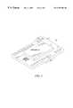
- FIG. 3illustrates a perspective view of the multi-chip integrated circuit shown in FIG. 2 .
- FIG. 4illustrates a side-elevational view of the multi-chip integrated circuit shown in FIG. 2-3.
- FIG. 5illustrates a partial-cutaway, partial-functional block, side-elevational view of an integrated circuit package which includes the multi-chip integrated circuit shown in FIGS. 2-4.
- FIG. 6illustrates a method flow diagram listing the method steps of the method of an embodiment of the present invention.
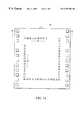
- a non-memory integrated circuit shown generally at 10includes a top-face surface 12 upon which a first plurality 14 and a second plurality 16 of mounting pads, respectively, are formed.
- the non-memory integrated circuitincludes circuit component portions which together form a circuit device, such as a logic device which performs logic functions.
- the integrated circuit 10includes the logic circuitry of a CPU (central processing unit).
- the integrated circuit 10forms a graphics controller.
- other circuitryis embodied in the integrated circuit 10 .
- the mounting pads 14permit electrical connection to an integrated circuit chip-on-chip mounted thereon. And, the mounting pads 16 provide for electrical connection with electrical interconnects (not shown) to other structure (also not shown).
- FIG. 1Billustrates a memory integrated circuit, shown generally at 18 , which, in an exemplary embodiment, is formed of a DRAM (dynamic random access memory), of a memory capacity great enough to permit appropriate amounts of data to be stored thereat.
- the memory device 18includes a bottom-face surface 22 having a plurality of mounting pads 24 formed thereon.
- the mounting pads 24correspond in number and position with the mounting pads 14 formed upon the top-face surface 12 of the integrated circuit 10 .
- the memory capacity of the memory integrated circuit 18is advantageously selected such that the memory requirements necessary for optimal operation of the logic circuitry forming the integrated circuit 10 is satisfied by the memory capacity of the memory integrated circuit 18 .
- the integrated circuits 10 and 18 of the exemplary illustrations shown in FIGS. 1A and 1Bshow an arrangement in which a single integrated circuit 18 is to be flip-chip mounted upon the top-face surface 12 of the integrated circuit 10
- one memory integrated circuit 18can be flip-chip mounted upon the top-face surface 12 , thereby to provide the logic circuitry embodied in the integrated circuit 10 with appropriate amounts of storage capacity.
- FIG. 2illustrates the multi-chip integrated circuit, shown generally at 30 , formed of the integrated circuit 10 upon which the memory integrated circuit 18 is flip-chip mounted thereon.
- the mounting pads 14 and 24 formed upon the top and bottom-face surfaces 12 and 22 , respectively, of the respective integrated circuitsare hidden from view in the Figure, but are aligned with one another to permit connections to be formed therebetween.
- FIG. 3also illustrates the multi-chip integrated circuit 30 formed of the non-memory integrated circuit 10 upon which the memory integrated circuit 18 is chip-on-chip mounted thereon.
- the mounting pads 14 and 24 of the integrated circuits 10is and 18 , respectively, are again hidden from view in the Figure.
- the mounting pads 16 formed upon the topface surface 12 of the integrated circuit 10are again illustrated in the Figure.
- the side-elevational view of FIG. 4illustrates the memory integrated circuit 18 flip-chip mounted upon the non-memory integrated circuit 10 .
- Solder balls 28further form portions of the multi-chip integrated circuit 30 .
- the solder balls 28correspond in number and positioning with the number and positioning of the mounting pads 14 and 24 of the integrated circuits 10 and 18 .
- the solder ballsare both electrically and mechanically affixed to the mounting pads 14 .
- the memory integrated circuit 18is connected to the integrated circuit 10 by aligning the solder balls 28 with the mounting pads 24 of the memory integrated circuit 18 and positioning the solder balls 28 and mounting pads 24 in a butting engagement theretogether.
- Solder connectionsfor example, are formed by increasing the ambient temperature levels to cause solder flow formed in conventional manner.
- the electrical interconnections between the memory integrated circuit 18 and the non-memory integrated circuit 10provide all necessary connections such as common input/output pads, control pads upon which RAS (row address select), WE (write enable), OE (output enable) and CAS (column address select), commands are generated, and power pads by which voltage and ground connections to the memory integrated circuit 18 are provided.
- connections so-formedare advantageously of low levels of capacitance. For instance, the levels of capacitance exhibited by input/output connections are reduced to about 0.5 pF in contrast to 30-100 pF of capacitance exhibited by conventional connections between separate chips. And, levels of the inductance of chip-to-chip interconnections are reduced substantially to zero in contrast to typical values of about 50 nH of inductance exhibited by connections formed in conventional fashion.
- the levels of capacitance and inductance of the interface formed of the mounting pad/solder ball combinationis lowered to an extent such that the interface appears to the memory integrated circuit 18 as an internal node of the memory device. Analogously, the interface also appears to the circuitry of the non-memory integrated circuit 10 to be merely an internal node thereof.
- the current, and therefore also power, in a circuitis directly proportional to the capacitance in the circuit. More particularly, the current in a circuit, and also the power, is equal to the capacitance in the circuit multiplied by the time rate of change of the voltage. Therefore, by reducing the level of capacitance, the time rate at which the voltage can be changed in a circuit can correspondingly be reduced.
- the interface formed of the mounting pad/solder ball combinationprovided through operation of an embodiment of the present invention permits an increase in speed at which the circuit can be operated as well as a decrease in the levels of power required to operate the circuit.
- the bandwidth of data transferred between the memory integrated circuit 18 and the integrated circuit 10can be increased.
- the total output current of the memory integrated circuit 18is governed by the following equation:
- I t(Number of I/O s)* C*V cc *freq/2
- I tis the total output current
- freqis the frequency at which the circuit is operated.
- the specifications to which the memory integrated circuit 18 must be constructedcan be altered. That is to say, when conventional connectors, such as bond wires, are used to connect the memory integrated circuit 18 with the non-memory circuitry embodied in a separate chip, the memory integrated circuit must be constructed to be able to drive a circuit including the capacitance exhibited by such conventional connections.
- the interface of an embodiment of the present inventionis utilized to form the connection between the memory integrated circuit 18 and the integrated circuit 10 , the memory integrated circuit 18 need only be constructed to drive a load which exhibits the lowered level of capacitance.
- FIG. 5illustrates a packaged integrated circuit, shown generally at 40 , of an embodiment of the present invention.
- the packaged integrated circuitincludes the chip-on-chip integrated circuit 30 shown in FIGS. 2-4.
- the integrated circuit 40is shown also to include the non-memory integrated circuit 10 , here a logic chip upon which the memory integrated circuit 18 is chip-on-chip mounted by way of solder balls 28 .
- the interface formed of the solder ball 28 /mounting pad 14 and 24 combinationis again formed as above-described. Namely, the interfaces formed of a plurality of solder balls 28 mechanically and electrically affixed to the non-memory integrated circuit 10 and solder-connected to the memory integrated circuit 18 .
- the packaged integrated circuit 40further includes a lead-frame pad 44 upon which the non-memory integrated circuit 10 is positioned.
- the pad 44is supported in an integrated circuit package 46 , in conventional fashion.
- Leads 48extend beyond the IC package 46 to permit connection to external circuitry (not shown), also in conventional fashion.
- Bond wires 52are also shown in the Figure. The bond wires 52 interconnect the mounting pads 16 with the leads 48 .
- the elements thereofappear to the respective integrated circuits essentially merely to be internal nodes of the respective circuits.
- Such lowered levels of capacitance and inductancefurther, for reasons above-described, permits increased speeds at which write and read operations to and from the storage locations of the memory device can be effectuated at reduced levels of power consumption.
- the memory integrated circuitcan be constructed to conform to specifications which require the memory integrated circuit to be able to drive loads of such lessened levels of capacitance.
- FIG. 6illustrates a method flow diagram, shown generally as 102 of an embodiment of the present invention.
- the method 102is a method for fabricating an integrated circuit.
- a memory chipis provided.
- the memory chipincludes a selected number of storage locations for storing data therein.
- the memory chipincludes a memory-chip face surface.
- a logic chipis provided.
- the logic chipincludes logic circuitry for performing a logic function.
- the logic chipincludes a logic-chip face surface.
- an interconnectoris formed upon at least one of the memory-chip face surface and the logic-chip face surface. Then, and as indicated by the block 112 , the memory chip and the logic chip are connected by positioning the memory chip and the logic chip in abutting engagement by way of the interconnector.
- Operation of an embodiment of the present inventionprovides a multi-chip, integrated-circuit package in which interconnections formed between the memory device and the logic chip are of substantially reduced levels of capacitance and inductance.
- Such reduced levels of capacitancereduces amounts of power required to operate a circuit formed of the memory and logic chips.
- Such reduced levels of capacitance and inductancealso permits the circuit to be operated at increased speeds.
Landscapes
- Engineering & Computer Science (AREA)
- Microelectronics & Electronic Packaging (AREA)
- Power Engineering (AREA)
- Physics & Mathematics (AREA)
- Condensed Matter Physics & Semiconductors (AREA)
- General Physics & Mathematics (AREA)
- Computer Hardware Design (AREA)
- Dram (AREA)
- Semiconductor Memories (AREA)
Abstract
Description
Claims (11)
Priority Applications (3)
| Application Number | Priority Date | Filing Date | Title |
|---|---|---|---|
| US09/190,660US6392304B1 (en) | 1998-11-12 | 1998-11-12 | Multi-chip memory apparatus and associated method |
| EP99308443AEP1001465A2 (en) | 1998-11-12 | 1999-10-26 | Multi-chip memory apparatus and associated method |
| US09/894,739US20010040281A1 (en) | 1998-11-12 | 2001-06-28 | Multi-chip memory apparatus and associated method |
Applications Claiming Priority (1)
| Application Number | Priority Date | Filing Date | Title |
|---|---|---|---|
| US09/190,660US6392304B1 (en) | 1998-11-12 | 1998-11-12 | Multi-chip memory apparatus and associated method |
Related Child Applications (1)
| Application Number | Title | Priority Date | Filing Date |
|---|---|---|---|
| US09/894,739DivisionUS20010040281A1 (en) | 1998-11-12 | 2001-06-28 | Multi-chip memory apparatus and associated method |
Publications (1)
| Publication Number | Publication Date |
|---|---|
| US6392304B1true US6392304B1 (en) | 2002-05-21 |
Family
ID=22702259
Family Applications (2)
| Application Number | Title | Priority Date | Filing Date |
|---|---|---|---|
| US09/190,660Expired - LifetimeUS6392304B1 (en) | 1998-11-12 | 1998-11-12 | Multi-chip memory apparatus and associated method |
| US09/894,739AbandonedUS20010040281A1 (en) | 1998-11-12 | 2001-06-28 | Multi-chip memory apparatus and associated method |
Family Applications After (1)
| Application Number | Title | Priority Date | Filing Date |
|---|---|---|---|
| US09/894,739AbandonedUS20010040281A1 (en) | 1998-11-12 | 2001-06-28 | Multi-chip memory apparatus and associated method |
Country Status (2)
| Country | Link |
|---|---|
| US (2) | US6392304B1 (en) |
| EP (1) | EP1001465A2 (en) |
Cited By (54)
| Publication number | Priority date | Publication date | Assignee | Title |
|---|---|---|---|---|
| US20030156442A1 (en)* | 2002-02-19 | 2003-08-21 | Matsushita Electric Industrial Co., Ltd. | Semiconductor memory device and multi-chip module comprising the semiconductor memory device |
| US20030173679A1 (en)* | 2002-03-13 | 2003-09-18 | Levardo Melvin N. | Stacked dice standoffs |
| US20040004280A1 (en)* | 2002-07-04 | 2004-01-08 | Manabu Shibata | Semiconductor device and system having semiconductor device mounted thereon |
| DE10244664A1 (en)* | 2002-09-24 | 2004-04-01 | Infineon Technologies Ag | Electronic component with semiconductor chips in a stack and method for producing the same |
| US20050001300A1 (en)* | 2003-07-02 | 2005-01-06 | Ho-Cheol Lee | Semiconductor package having multiple embedded chips |
| US20050156616A1 (en)* | 2004-01-20 | 2005-07-21 | Nec Electronics Corporation | Integrated circuit device |
| US20050161794A1 (en)* | 2001-03-30 | 2005-07-28 | Fujitsu Limited | Semiconductor device, method for manufacturing the semiconductor device and semiconductor substrate |
| US20050170600A1 (en)* | 2004-01-29 | 2005-08-04 | Yukio Fukuzo | Three-dimensional semiconductor package, and spacer chip used therein |
| US20050167798A1 (en)* | 2004-01-29 | 2005-08-04 | Doan Trung T. | Die-wafer package and method of fabricating same |
| US20050251586A1 (en)* | 1999-02-08 | 2005-11-10 | Megic Corporation | Multiple selectable function integrated circuit module |
| US20070058410A1 (en)* | 2005-09-02 | 2007-03-15 | Rajan Suresh N | Methods and apparatus of stacking DRAMs |
| US20070120267A1 (en)* | 2005-11-28 | 2007-05-31 | Hiroshi Kuroda | Multi chip module |
| US20070135055A1 (en)* | 2005-12-13 | 2007-06-14 | Ho Lee S | Combination quad flat no-lead and thin small outline package |
| US20070290363A1 (en)* | 2006-06-16 | 2007-12-20 | Kye-Hyun Kyung | Semiconductor device having interface chip including penetrating electrode |
| US20080025123A1 (en)* | 2006-07-31 | 2008-01-31 | Metaram, Inc. | Interface circuit system and method for autonomously performing power management operations in conjunction with a plurality of memory circuits |
| US20080025125A1 (en)* | 2006-07-31 | 2008-01-31 | Metaram, Inc. | Interface circuit system and method for performing power management operations in conjunction with only a portion of a memory circuit |
| US20080025124A1 (en)* | 2006-07-31 | 2008-01-31 | Metaram, Inc. | Interface circuit system and method for performing power management operations utilizing power management signals |
| US20080211081A1 (en)* | 2006-12-05 | 2008-09-04 | Samsung Electronics Co., Ltd. | Planar multi semiconductor chip package and method of manufacturing the same |
| US7515453B2 (en) | 2005-06-24 | 2009-04-07 | Metaram, Inc. | Integrated memory core and memory interface circuit |
| US20090174082A1 (en)* | 1997-04-04 | 2009-07-09 | Glenn J Leedy | Three dimensional structure memory |
| US7581127B2 (en) | 2006-07-31 | 2009-08-25 | Metaram, Inc. | Interface circuit system and method for performing power saving operations during a command-related latency |
| US7580312B2 (en) | 2006-07-31 | 2009-08-25 | Metaram, Inc. | Power saving system and method for use with a plurality of memory circuits |
| US7609567B2 (en) | 2005-06-24 | 2009-10-27 | Metaram, Inc. | System and method for simulating an aspect of a memory circuit |
| US20100117242A1 (en)* | 2008-11-10 | 2010-05-13 | Miller Gary L | Technique for packaging multiple integrated circuits |
| US7724589B2 (en) | 2006-07-31 | 2010-05-25 | Google Inc. | System and method for delaying a signal communicated from a system to at least one of a plurality of memory circuits |
| US8041881B2 (en) | 2006-07-31 | 2011-10-18 | Google Inc. | Memory device with emulated characteristics |
| US8055833B2 (en) | 2006-10-05 | 2011-11-08 | Google Inc. | System and method for increasing capacity, performance, and flexibility of flash storage |
| US8060774B2 (en) | 2005-06-24 | 2011-11-15 | Google Inc. | Memory systems and memory modules |
| US8077535B2 (en) | 2006-07-31 | 2011-12-13 | Google Inc. | Memory refresh apparatus and method |
| US8080442B2 (en) | 2002-08-08 | 2011-12-20 | Elm Technology Corporation | Vertical system integration |
| US8080874B1 (en) | 2007-09-14 | 2011-12-20 | Google Inc. | Providing additional space between an integrated circuit and a circuit board for positioning a component therebetween |
| US8081474B1 (en) | 2007-12-18 | 2011-12-20 | Google Inc. | Embossed heat spreader |
| US8090897B2 (en) | 2006-07-31 | 2012-01-03 | Google Inc. | System and method for simulating an aspect of a memory circuit |
| US8089795B2 (en) | 2006-02-09 | 2012-01-03 | Google Inc. | Memory module with memory stack and interface with enhanced capabilities |
| US8111566B1 (en) | 2007-11-16 | 2012-02-07 | Google, Inc. | Optimal channel design for memory devices for providing a high-speed memory interface |
| US8130560B1 (en) | 2006-11-13 | 2012-03-06 | Google Inc. | Multi-rank partial width memory modules |
| US8169233B2 (en) | 2009-06-09 | 2012-05-01 | Google Inc. | Programming of DIMM termination resistance values |
| US8209479B2 (en) | 2007-07-18 | 2012-06-26 | Google Inc. | Memory circuit system and method |
| US8244971B2 (en) | 2006-07-31 | 2012-08-14 | Google Inc. | Memory circuit system and method |
| US8280714B2 (en) | 2006-07-31 | 2012-10-02 | Google Inc. | Memory circuit simulation system and method with refresh capabilities |
| US8327104B2 (en) | 2006-07-31 | 2012-12-04 | Google Inc. | Adjusting the timing of signals associated with a memory system |
| US8335894B1 (en) | 2008-07-25 | 2012-12-18 | Google Inc. | Configurable memory system with interface circuit |
| US8386722B1 (en) | 2008-06-23 | 2013-02-26 | Google Inc. | Stacked DIMM memory interface |
| US8397013B1 (en) | 2006-10-05 | 2013-03-12 | Google Inc. | Hybrid memory module |
| US20130070507A1 (en)* | 2011-09-19 | 2013-03-21 | Tae-Young Yoon | Semiconductor memory device |
| US8438328B2 (en) | 2008-02-21 | 2013-05-07 | Google Inc. | Emulation of abstracted DIMMs using abstracted DRAMs |
| US8566516B2 (en) | 2006-07-31 | 2013-10-22 | Google Inc. | Refresh management of memory modules |
| US8796830B1 (en) | 2006-09-01 | 2014-08-05 | Google Inc. | Stackable low-profile lead frame package |
| US8972673B2 (en) | 2006-07-31 | 2015-03-03 | Google Inc. | Power management of memory circuits by virtual memory simulation |
| US9171585B2 (en) | 2005-06-24 | 2015-10-27 | Google Inc. | Configurable memory circuit system and method |
| US9507739B2 (en) | 2005-06-24 | 2016-11-29 | Google Inc. | Configurable memory circuit system and method |
| US9542353B2 (en) | 2006-02-09 | 2017-01-10 | Google Inc. | System and method for reducing command scheduling constraints of memory circuits |
| US9632929B2 (en) | 2006-02-09 | 2017-04-25 | Google Inc. | Translating an address associated with a command communicated between a system and memory circuits |
| US10013371B2 (en) | 2005-06-24 | 2018-07-03 | Google Llc | Configurable memory circuit system and method |
Families Citing this family (14)
| Publication number | Priority date | Publication date | Assignee | Title |
|---|---|---|---|---|
| JP2002124626A (en)* | 2000-10-16 | 2002-04-26 | Hitachi Ltd | Semiconductor device |
| DE10124774B4 (en)* | 2001-05-21 | 2016-05-25 | Infineon Technologies Ag | Semiconductor component having at least one semiconductor chip on a base chip serving as substrate and method for its production |
| JP2003023138A (en)* | 2001-07-10 | 2003-01-24 | Toshiba Corp | Memory chip, COC device using the same, and methods of manufacturing these |
| US20030089998A1 (en)* | 2001-11-09 | 2003-05-15 | Chan Vincent K. | Direct interconnect multi-chip module, method for making the same and electronic package comprising same |
| WO2003065453A1 (en)* | 2002-01-31 | 2003-08-07 | Micronas Gmbh | Receptacle for a programmable, electronic processing device |
| US6979904B2 (en)* | 2002-04-19 | 2005-12-27 | Micron Technology, Inc. | Integrated circuit package having reduced interconnects |
| DE10332829B4 (en)* | 2003-07-18 | 2007-11-08 | Infineon Technologies Ag | Semiconductor chip stack |
| US7170315B2 (en) | 2003-07-31 | 2007-01-30 | Actel Corporation | Programmable system on a chip |
| EP1598868A1 (en)* | 2004-05-18 | 2005-11-23 | Texas Instruments Inc. | Stacked dies having shared access to memory |
| US7459772B2 (en)* | 2004-09-29 | 2008-12-02 | Actel Corporation | Face-to-face bonded I/O circuit die and functional logic circuit die system |
| DE102006034679A1 (en)* | 2006-07-24 | 2008-01-31 | Infineon Technologies Ag | Semiconductor module with power semiconductor chip and passive component and method for producing the same |
| US10840239B2 (en)* | 2014-08-26 | 2020-11-17 | Monolithic 3D Inc. | 3D semiconductor device and structure |
| CN106876285B (en)* | 2017-01-16 | 2018-09-21 | 建荣半导体(深圳)有限公司 | A kind of chip packing-body and its method, chip, video recording equipment and electronic equipment |
| CN115132719B (en)* | 2021-03-26 | 2025-01-28 | 世芯电子股份有限公司 | Integrated circuit products and their chip layout |
Citations (8)
| Publication number | Priority date | Publication date | Assignee | Title |
|---|---|---|---|---|
| US4983533A (en) | 1987-10-28 | 1991-01-08 | Irvine Sensors Corporation | High-density electronic modules - process and product |
| US5347428A (en) | 1992-12-03 | 1994-09-13 | Irvine Sensors Corporation | Module comprising IC memory stack dedicated to and structurally combined with an IC microprocessor chip |
| US5468681A (en) | 1989-08-28 | 1995-11-21 | Lsi Logic Corporation | Process for interconnecting conductive substrates using an interposer having conductive plastic filled vias |
| US5537738A (en) | 1995-02-10 | 1996-07-23 | Micron Display Technology Inc. | Methods of mechanical and electrical substrate connection |
| US5561622A (en) | 1993-09-13 | 1996-10-01 | International Business Machines Corporation | Integrated memory cube structure |
| US5702984A (en) | 1993-09-13 | 1997-12-30 | International Business Machines Corporation | Integrated mulitchip memory module, structure and fabrication |
| US5790384A (en)* | 1997-06-26 | 1998-08-04 | International Business Machines Corporation | Bare die multiple dies for direct attach |
| US6084308A (en)* | 1998-06-30 | 2000-07-04 | National Semiconductor Corporation | Chip-on-chip integrated circuit package and method for making the same |
- 1998
- 1998-11-12USUS09/190,660patent/US6392304B1/ennot_activeExpired - Lifetime
- 1999
- 1999-10-26EPEP99308443Apatent/EP1001465A2/ennot_activeWithdrawn
- 2001
- 2001-06-28USUS09/894,739patent/US20010040281A1/ennot_activeAbandoned
Patent Citations (9)
| Publication number | Priority date | Publication date | Assignee | Title |
|---|---|---|---|---|
| US4983533A (en) | 1987-10-28 | 1991-01-08 | Irvine Sensors Corporation | High-density electronic modules - process and product |
| US5468681A (en) | 1989-08-28 | 1995-11-21 | Lsi Logic Corporation | Process for interconnecting conductive substrates using an interposer having conductive plastic filled vias |
| US5347428A (en) | 1992-12-03 | 1994-09-13 | Irvine Sensors Corporation | Module comprising IC memory stack dedicated to and structurally combined with an IC microprocessor chip |
| US5561622A (en) | 1993-09-13 | 1996-10-01 | International Business Machines Corporation | Integrated memory cube structure |
| US5563086A (en) | 1993-09-13 | 1996-10-08 | International Business Machines Corporation | Integrated memory cube, structure and fabrication |
| US5702984A (en) | 1993-09-13 | 1997-12-30 | International Business Machines Corporation | Integrated mulitchip memory module, structure and fabrication |
| US5537738A (en) | 1995-02-10 | 1996-07-23 | Micron Display Technology Inc. | Methods of mechanical and electrical substrate connection |
| US5790384A (en)* | 1997-06-26 | 1998-08-04 | International Business Machines Corporation | Bare die multiple dies for direct attach |
| US6084308A (en)* | 1998-06-30 | 2000-07-04 | National Semiconductor Corporation | Chip-on-chip integrated circuit package and method for making the same |
Non-Patent Citations (2)
| Title |
|---|
| Al-Sarawi, Said F., Flip-chip Bonded Stacked Chips without Spacers, Centre for High Performance Integrated Technologies and Systems (CHIPTEC), Adelaide, SA 5005, Internet site: http://www.eleceng.adelaide.edu.au/Person . . . ing/node37.html, Mar. 1997. |
| Al-Sarawi, Said F., Solder Bump Bonding, Centre for High Performance Integrated Technologies and Systems (CHIPTEC), Adelaide, SA 5005, Internet site: http://www.eleceng.adelaide.edu.au/Person . . . ing/node37.html, Mar. 1997. |
Cited By (136)
| Publication number | Priority date | Publication date | Assignee | Title |
|---|---|---|---|---|
| US20110198672A1 (en)* | 1997-04-04 | 2011-08-18 | Leedy Glenn J | Three dimensional structure memory |
| US9401183B2 (en) | 1997-04-04 | 2016-07-26 | Glenn J. Leedy | Stacked integrated memory device |
| US20090230501A1 (en)* | 1997-04-04 | 2009-09-17 | Leedy Glenn J | Three dimensional structure memory |
| US8933570B2 (en) | 1997-04-04 | 2015-01-13 | Elm Technology Corp. | Three dimensional structure memory |
| US20090219742A1 (en)* | 1997-04-04 | 2009-09-03 | Leedy Glenn J | Three dimensional structure memory |
| US20090219772A1 (en)* | 1997-04-04 | 2009-09-03 | Leedy Glenn J | Three dimensional structure memory |
| US9087556B2 (en) | 1997-04-04 | 2015-07-21 | Glenn J Leedy | Three dimension structure memory |
| US8841778B2 (en) | 1997-04-04 | 2014-09-23 | Glenn J Leedy | Three dimensional memory structure |
| US20090174082A1 (en)* | 1997-04-04 | 2009-07-09 | Glenn J Leedy | Three dimensional structure memory |
| US8796862B2 (en) | 1997-04-04 | 2014-08-05 | Glenn J Leedy | Three dimensional memory structure |
| US8410617B2 (en) | 1997-04-04 | 2013-04-02 | Elm Technology | Three dimensional structure memory |
| US8318538B2 (en) | 1997-04-04 | 2012-11-27 | Elm Technology Corp. | Three dimensional structure memory |
| US8928119B2 (en)* | 1997-04-04 | 2015-01-06 | Glenn J. Leedy | Three dimensional structure memory |
| US8791581B2 (en) | 1997-04-04 | 2014-07-29 | Glenn J Leedy | Three dimensional structure memory |
| US8907499B2 (en) | 1997-04-04 | 2014-12-09 | Glenn J Leedy | Three dimensional structure memory |
| US8653672B2 (en) | 1997-04-04 | 2014-02-18 | Glenn J Leedy | Three dimensional structure memory |
| US8629542B2 (en) | 1997-04-04 | 2014-01-14 | Glenn J. Leedy | Three dimensional structure memory |
| US8035233B2 (en) | 1997-04-04 | 2011-10-11 | Elm Technology Corporation | Adjacent substantially flexible substrates having integrated circuits that are bonded together by non-polymeric layer |
| US8288206B2 (en) | 1997-04-04 | 2012-10-16 | Elm Technology Corp | Three dimensional structure memory |
| US20100172197A1 (en)* | 1997-04-04 | 2010-07-08 | Leedy Glenn J | Three dimensional structure memory |
| US8824159B2 (en) | 1997-04-04 | 2014-09-02 | Glenn J. Leedy | Three dimensional structure memory |
| US7372162B2 (en)* | 1999-02-08 | 2008-05-13 | Megica Corporation | Multiple selectable function integrated circuit module |
| US20080185736A1 (en)* | 1999-02-08 | 2008-08-07 | Megica Corporation | Multiple selectable function integrated circuit module |
| US8471389B2 (en)* | 1999-02-08 | 2013-06-25 | Megica Corporation | Multiple selectable function integrated circuit module |
| US8013448B2 (en) | 1999-02-08 | 2011-09-06 | Megica Corporation | Multiple selectable function integrated circuit module |
| US20110285018A1 (en)* | 1999-02-08 | 2011-11-24 | Megica Corporation | Multiple selectable function integrated circuit module |
| US20050251586A1 (en)* | 1999-02-08 | 2005-11-10 | Megic Corporation | Multiple selectable function integrated circuit module |
| US20060226529A1 (en)* | 2001-03-30 | 2006-10-12 | Fujitsu Limited | Semiconductor device, method for manufacturing the semiconductor device and semiconductor substrate |
| US6972487B2 (en)* | 2001-03-30 | 2005-12-06 | Fujitsu Limited | Multi chip package structure having a plurality of semiconductor chips mounted in the same package |
| US20050161794A1 (en)* | 2001-03-30 | 2005-07-28 | Fujitsu Limited | Semiconductor device, method for manufacturing the semiconductor device and semiconductor substrate |
| US20050205983A1 (en)* | 2002-02-19 | 2005-09-22 | Matsushita Electric Industrial Co., Ltd. | Semiconductor memory device and multi-chip module comprising the semiconductor memory device |
| US7072241B2 (en) | 2002-02-19 | 2006-07-04 | Matsushita Electric Industrial Co., Ltd. | Semiconductor memory device and multi-chip module comprising the semiconductor memory device |
| US20030156442A1 (en)* | 2002-02-19 | 2003-08-21 | Matsushita Electric Industrial Co., Ltd. | Semiconductor memory device and multi-chip module comprising the semiconductor memory device |
| US20030173679A1 (en)* | 2002-03-13 | 2003-09-18 | Levardo Melvin N. | Stacked dice standoffs |
| US6753613B2 (en)* | 2002-03-13 | 2004-06-22 | Intel Corporation | Stacked dice standoffs |
| US20060286714A1 (en)* | 2002-07-04 | 2006-12-21 | Manabu Shibata | Semiconductor device and system having semiconductor device mounted thereon |
| US20040004280A1 (en)* | 2002-07-04 | 2004-01-08 | Manabu Shibata | Semiconductor device and system having semiconductor device mounted thereon |
| US7224054B2 (en)* | 2002-07-04 | 2007-05-29 | Fujitsu Limited | Semiconductor device and system having semiconductor device mounted thereon |
| US8269327B2 (en) | 2002-08-08 | 2012-09-18 | Glenn J Leedy | Vertical system integration |
| US8587102B2 (en) | 2002-08-08 | 2013-11-19 | Glenn J Leedy | Vertical system integration |
| US8080442B2 (en) | 2002-08-08 | 2011-12-20 | Elm Technology Corporation | Vertical system integration |
| US20040063304A1 (en)* | 2002-09-24 | 2004-04-01 | Robert-Christian Hagen | Electronic component with a stack of semiconductor chips and a method for producing the electronic component |
| DE10244664A8 (en) | 2002-09-24 | 2004-07-15 | Infineon Technologies Ag | Electronic component with semiconductor chips in a stack and method for producing the same |
| DE10244664A1 (en)* | 2002-09-24 | 2004-04-01 | Infineon Technologies Ag | Electronic component with semiconductor chips in a stack and method for producing the same |
| US7190059B2 (en)* | 2002-09-24 | 2007-03-13 | Infineon Technologies Ag | Electronic component with a stack of semiconductor chips and a method for producing the electronic component |
| US20050001300A1 (en)* | 2003-07-02 | 2005-01-06 | Ho-Cheol Lee | Semiconductor package having multiple embedded chips |
| US7170157B2 (en)* | 2003-07-02 | 2007-01-30 | Samsung Electronics Co., Ltd. | Semiconductor package having multiple embedded chips |
| US7400134B2 (en) | 2004-01-20 | 2008-07-15 | Nec Electronics Corporation | Integrated circuit device with multiple chips in one package |
| US20050156616A1 (en)* | 2004-01-20 | 2005-07-21 | Nec Electronics Corporation | Integrated circuit device |
| US20090011540A1 (en)* | 2004-01-29 | 2009-01-08 | Micron Technology, Inc. | Die-wafer package and method of fabricating same |
| US7413928B2 (en) | 2004-01-29 | 2008-08-19 | Micron Technology, Inc. | Die-wafer package and method of fabricating same |
| US20060264023A1 (en)* | 2004-01-29 | 2006-11-23 | Doan Trung T | Die-wafer package and method of fabricating same |
| US7122906B2 (en) | 2004-01-29 | 2006-10-17 | Micron Technology, Inc. | Die-wafer package and method of fabricating same |
| US20050167798A1 (en)* | 2004-01-29 | 2005-08-04 | Doan Trung T. | Die-wafer package and method of fabricating same |
| US20050170600A1 (en)* | 2004-01-29 | 2005-08-04 | Yukio Fukuzo | Three-dimensional semiconductor package, and spacer chip used therein |
| US7807503B2 (en) | 2004-01-29 | 2010-10-05 | Micron Technology, Inc. | Die-wafer package and method of fabricating same |
| US8359187B2 (en) | 2005-06-24 | 2013-01-22 | Google Inc. | Simulating a different number of memory circuit devices |
| US9507739B2 (en) | 2005-06-24 | 2016-11-29 | Google Inc. | Configurable memory circuit system and method |
| US8386833B2 (en) | 2005-06-24 | 2013-02-26 | Google Inc. | Memory systems and memory modules |
| US8773937B2 (en) | 2005-06-24 | 2014-07-08 | Google Inc. | Memory refresh apparatus and method |
| US7515453B2 (en) | 2005-06-24 | 2009-04-07 | Metaram, Inc. | Integrated memory core and memory interface circuit |
| US8060774B2 (en) | 2005-06-24 | 2011-11-15 | Google Inc. | Memory systems and memory modules |
| US9171585B2 (en) | 2005-06-24 | 2015-10-27 | Google Inc. | Configurable memory circuit system and method |
| US7609567B2 (en) | 2005-06-24 | 2009-10-27 | Metaram, Inc. | System and method for simulating an aspect of a memory circuit |
| US8615679B2 (en) | 2005-06-24 | 2013-12-24 | Google Inc. | Memory modules with reliability and serviceability functions |
| US10013371B2 (en) | 2005-06-24 | 2018-07-03 | Google Llc | Configurable memory circuit system and method |
| US8582339B2 (en) | 2005-09-02 | 2013-11-12 | Google Inc. | System including memory stacks |
| US8811065B2 (en) | 2005-09-02 | 2014-08-19 | Google Inc. | Performing error detection on DRAMs |
| US7379316B2 (en) | 2005-09-02 | 2008-05-27 | Metaram, Inc. | Methods and apparatus of stacking DRAMs |
| US20070058410A1 (en)* | 2005-09-02 | 2007-03-15 | Rajan Suresh N | Methods and apparatus of stacking DRAMs |
| US8619452B2 (en) | 2005-09-02 | 2013-12-31 | Google Inc. | Methods and apparatus of stacking DRAMs |
| US20070120267A1 (en)* | 2005-11-28 | 2007-05-31 | Hiroshi Kuroda | Multi chip module |
| US7656039B2 (en)* | 2005-11-28 | 2010-02-02 | Renesas Technology Corp. | Multi chip module |
| US20070135055A1 (en)* | 2005-12-13 | 2007-06-14 | Ho Lee S | Combination quad flat no-lead and thin small outline package |
| US9632929B2 (en) | 2006-02-09 | 2017-04-25 | Google Inc. | Translating an address associated with a command communicated between a system and memory circuits |
| US9727458B2 (en) | 2006-02-09 | 2017-08-08 | Google Inc. | Translating an address associated with a command communicated between a system and memory circuits |
| US8566556B2 (en) | 2006-02-09 | 2013-10-22 | Google Inc. | Memory module with memory stack and interface with enhanced capabilities |
| US9542352B2 (en) | 2006-02-09 | 2017-01-10 | Google Inc. | System and method for reducing command scheduling constraints of memory circuits |
| US8797779B2 (en) | 2006-02-09 | 2014-08-05 | Google Inc. | Memory module with memory stack and interface with enhanced capabilites |
| US8089795B2 (en) | 2006-02-09 | 2012-01-03 | Google Inc. | Memory module with memory stack and interface with enhanced capabilities |
| US9542353B2 (en) | 2006-02-09 | 2017-01-10 | Google Inc. | System and method for reducing command scheduling constraints of memory circuits |
| US20070290363A1 (en)* | 2006-06-16 | 2007-12-20 | Kye-Hyun Kyung | Semiconductor device having interface chip including penetrating electrode |
| US8090897B2 (en) | 2006-07-31 | 2012-01-03 | Google Inc. | System and method for simulating an aspect of a memory circuit |
| US8244971B2 (en) | 2006-07-31 | 2012-08-14 | Google Inc. | Memory circuit system and method |
| US8745321B2 (en) | 2006-07-31 | 2014-06-03 | Google Inc. | Simulating a memory standard |
| US20080025123A1 (en)* | 2006-07-31 | 2008-01-31 | Metaram, Inc. | Interface circuit system and method for autonomously performing power management operations in conjunction with a plurality of memory circuits |
| US20080025125A1 (en)* | 2006-07-31 | 2008-01-31 | Metaram, Inc. | Interface circuit system and method for performing power management operations in conjunction with only a portion of a memory circuit |
| US8077535B2 (en) | 2006-07-31 | 2011-12-13 | Google Inc. | Memory refresh apparatus and method |
| US20080025124A1 (en)* | 2006-07-31 | 2008-01-31 | Metaram, Inc. | Interface circuit system and method for performing power management operations utilizing power management signals |
| US8327104B2 (en) | 2006-07-31 | 2012-12-04 | Google Inc. | Adjusting the timing of signals associated with a memory system |
| US7386656B2 (en) | 2006-07-31 | 2008-06-10 | Metaram, Inc. | Interface circuit system and method for performing power management operations in conjunction with only a portion of a memory circuit |
| US7590796B2 (en) | 2006-07-31 | 2009-09-15 | Metaram, Inc. | System and method for power management in memory systems |
| US7724589B2 (en) | 2006-07-31 | 2010-05-25 | Google Inc. | System and method for delaying a signal communicated from a system to at least one of a plurality of memory circuits |
| US8566516B2 (en) | 2006-07-31 | 2013-10-22 | Google Inc. | Refresh management of memory modules |
| US8280714B2 (en) | 2006-07-31 | 2012-10-02 | Google Inc. | Memory circuit simulation system and method with refresh capabilities |
| US8041881B2 (en) | 2006-07-31 | 2011-10-18 | Google Inc. | Memory device with emulated characteristics |
| US8340953B2 (en) | 2006-07-31 | 2012-12-25 | Google, Inc. | Memory circuit simulation with power saving capabilities |
| US7392338B2 (en) | 2006-07-31 | 2008-06-24 | Metaram, Inc. | Interface circuit system and method for autonomously performing power management operations in conjunction with a plurality of memory circuits |
| US8154935B2 (en) | 2006-07-31 | 2012-04-10 | Google Inc. | Delaying a signal communicated from a system to at least one of a plurality of memory circuits |
| US8631220B2 (en) | 2006-07-31 | 2014-01-14 | Google Inc. | Adjusting the timing of signals associated with a memory system |
| US8972673B2 (en) | 2006-07-31 | 2015-03-03 | Google Inc. | Power management of memory circuits by virtual memory simulation |
| US8868829B2 (en) | 2006-07-31 | 2014-10-21 | Google Inc. | Memory circuit system and method |
| US7472220B2 (en) | 2006-07-31 | 2008-12-30 | Metaram, Inc. | Interface circuit system and method for performing power management operations utilizing power management signals |
| US7581127B2 (en) | 2006-07-31 | 2009-08-25 | Metaram, Inc. | Interface circuit system and method for performing power saving operations during a command-related latency |
| US7580312B2 (en) | 2006-07-31 | 2009-08-25 | Metaram, Inc. | Power saving system and method for use with a plurality of memory circuits |
| US9047976B2 (en) | 2006-07-31 | 2015-06-02 | Google Inc. | Combined signal delay and power saving for use with a plurality of memory circuits |
| US8796830B1 (en) | 2006-09-01 | 2014-08-05 | Google Inc. | Stackable low-profile lead frame package |
| US8751732B2 (en) | 2006-10-05 | 2014-06-10 | Google Inc. | System and method for increasing capacity, performance, and flexibility of flash storage |
| US8977806B1 (en) | 2006-10-05 | 2015-03-10 | Google Inc. | Hybrid memory module |
| US8397013B1 (en) | 2006-10-05 | 2013-03-12 | Google Inc. | Hybrid memory module |
| US8055833B2 (en) | 2006-10-05 | 2011-11-08 | Google Inc. | System and method for increasing capacity, performance, and flexibility of flash storage |
| US8370566B2 (en) | 2006-10-05 | 2013-02-05 | Google Inc. | System and method for increasing capacity, performance, and flexibility of flash storage |
| US8760936B1 (en) | 2006-11-13 | 2014-06-24 | Google Inc. | Multi-rank partial width memory modules |
| US8130560B1 (en) | 2006-11-13 | 2012-03-06 | Google Inc. | Multi-rank partial width memory modules |
| US8446781B1 (en) | 2006-11-13 | 2013-05-21 | Google Inc. | Multi-rank partial width memory modules |
| US8319351B2 (en) | 2006-12-05 | 2012-11-27 | Samsung Electronics Co., Ltd. | Planar multi semiconductor chip package |
| US7675181B2 (en) | 2006-12-05 | 2010-03-09 | Samsung Electronics Co., Ltd. | Planar multi semiconductor chip package and method of manufacturing the same |
| US20080211081A1 (en)* | 2006-12-05 | 2008-09-04 | Samsung Electronics Co., Ltd. | Planar multi semiconductor chip package and method of manufacturing the same |
| US20100117215A1 (en)* | 2006-12-05 | 2010-05-13 | Jong-Joo Lee | Planar multi semiconductor chip package |
| US8209479B2 (en) | 2007-07-18 | 2012-06-26 | Google Inc. | Memory circuit system and method |
| US8080874B1 (en) | 2007-09-14 | 2011-12-20 | Google Inc. | Providing additional space between an integrated circuit and a circuit board for positioning a component therebetween |
| US8111566B1 (en) | 2007-11-16 | 2012-02-07 | Google, Inc. | Optimal channel design for memory devices for providing a high-speed memory interface |
| US8675429B1 (en) | 2007-11-16 | 2014-03-18 | Google Inc. | Optimal channel design for memory devices for providing a high-speed memory interface |
| US8081474B1 (en) | 2007-12-18 | 2011-12-20 | Google Inc. | Embossed heat spreader |
| US8730670B1 (en) | 2007-12-18 | 2014-05-20 | Google Inc. | Embossed heat spreader |
| US8705240B1 (en) | 2007-12-18 | 2014-04-22 | Google Inc. | Embossed heat spreader |
| US8631193B2 (en) | 2008-02-21 | 2014-01-14 | Google Inc. | Emulation of abstracted DIMMS using abstracted DRAMS |
| US8438328B2 (en) | 2008-02-21 | 2013-05-07 | Google Inc. | Emulation of abstracted DIMMs using abstracted DRAMs |
| US8762675B2 (en) | 2008-06-23 | 2014-06-24 | Google Inc. | Memory system for synchronous data transmission |
| US8386722B1 (en) | 2008-06-23 | 2013-02-26 | Google Inc. | Stacked DIMM memory interface |
| US8819356B2 (en) | 2008-07-25 | 2014-08-26 | Google Inc. | Configurable multirank memory system with interface circuit |
| US8335894B1 (en) | 2008-07-25 | 2012-12-18 | Google Inc. | Configurable memory system with interface circuit |
| US20100117242A1 (en)* | 2008-11-10 | 2010-05-13 | Miller Gary L | Technique for packaging multiple integrated circuits |
| US8169233B2 (en) | 2009-06-09 | 2012-05-01 | Google Inc. | Programming of DIMM termination resistance values |
| US8811055B2 (en)* | 2011-09-19 | 2014-08-19 | Samsung Electronics Co., Ltd. | Semiconductor memory device |
| US20130070507A1 (en)* | 2011-09-19 | 2013-03-21 | Tae-Young Yoon | Semiconductor memory device |
Also Published As
| Publication number | Publication date |
|---|---|
| US20010040281A1 (en) | 2001-11-15 |
| EP1001465A2 (en) | 2000-05-17 |
Similar Documents
| Publication | Publication Date | Title |
|---|---|---|
| US6392304B1 (en) | Multi-chip memory apparatus and associated method | |
| US6768660B2 (en) | Multi-chip memory devices and modules including independent control of memory chips | |
| US6740981B2 (en) | Semiconductor device including memory unit and semiconductor module including memory units | |
| US8637998B2 (en) | Semiconductor chip and semiconductor device | |
| EP0707316B1 (en) | Semiconductor device with memory core chip and memory peripheral circuit chip and method for fabricating the same | |
| KR100430984B1 (en) | Semiconductor device | |
| US6847575B2 (en) | Semiconductor device including multi-chip | |
| US7872936B2 (en) | System and method for packaged memory | |
| US20040145042A1 (en) | Semiconductor device | |
| US6381141B2 (en) | Integrated device and method for routing a signal through the device | |
| US10586775B2 (en) | Memory packages and related semiconductor packages | |
| US9613678B2 (en) | Semiconductor apparatus including multichip package | |
| JPH08167703A (en) | Semiconductor device, manufacturing method thereof, memory core chip, and memory peripheral circuit chip | |
| US6594167B1 (en) | Semiconductor integrated circuit having a structure for equalizing interconnection lengths and memory module provided with the semiconductor integrated circuit | |
| US7005748B2 (en) | Flip chip interface circuit of a semiconductor memory device | |
| US6879036B2 (en) | Semiconductor memory device and method of manufacturing semiconductor device with chip on chip structure | |
| KR100585331B1 (en) | Semiconductor device and memory system | |
| JP2003282813A (en) | Semiconductor device, memory core part chip, memory peripheral circuit part chip, and semiconductor memory device | |
| JPH02224266A (en) | semiconductor equipment | |
| JP2006294244A (en) | Semiconductor device, memory core part chip, memory peripheral circuit part chip, and semiconductor memory device |
Legal Events
| Date | Code | Title | Description |
|---|---|---|---|
| AS | Assignment | Owner name:NIPPON STEEL SEMICONDUCTOR CORPORATION, JAPAN Free format text:ASSIGNMENT OF ASSIGNORS INTEREST;ASSIGNOR:BUTLER, DOUGLAS B.;REEL/FRAME:009584/0081 Effective date:19981109 Owner name:UNITED MEMORIES, INC., COLORADO Free format text:ASSIGNMENT OF ASSIGNORS INTEREST;ASSIGNOR:BUTLER, DOUGLAS B.;REEL/FRAME:009584/0081 Effective date:19981109 | |
| STCF | Information on status: patent grant | Free format text:PATENTED CASE | |
| AS | Assignment | Owner name:PROMOS TECHNOLOGIES INC., TAIWAN Free format text:ASSIGNMENT OF ASSIGNORS INTEREST;ASSIGNOR:MOSEL VITELIC, INC.;REEL/FRAME:015334/0772 Effective date:20040427 | |
| FPAY | Fee payment | Year of fee payment:4 | |
| FPAY | Fee payment | Year of fee payment:8 | |
| AS | Assignment | Owner name:MARSHALL MICROCHIP HOLDING COMPANY, TEXAS Free format text:ASSIGNMENT OF ASSIGNORS INTEREST;ASSIGNOR:PROMOS TECHNOLOGIES, INC.;REEL/FRAME:023449/0896 Effective date:20091009 | |
| AS | Assignment | Owner name:PATENT BUSINESS DEVELOPMENT, LLC, FLORIDA Free format text:ASSIGNMENT OF ASSIGNORS INTEREST;ASSIGNOR:MARSHALL MICROCHIP HOLDING COMPANY;REEL/FRAME:025934/0163 Effective date:20110125 | |
| FPAY | Fee payment | Year of fee payment:12 | |
| AS | Assignment | Owner name:CHIP PACKAGING SOLUTIONS LLC, TEXAS Free format text:ASSIGNMENT OF ASSIGNORS INTEREST;ASSIGNOR:ACACIA RESEARCH GROUP LLC;REEL/FRAME:030636/0181 Effective date:20120210 Owner name:ACACIA RESEARCH GROUP LLC, TEXAS Free format text:ASSIGNMENT OF ASSIGNORS INTEREST;ASSIGNOR:PATENT BUSINESS DEVELOPMENT LLC;REEL/FRAME:030650/0472 Effective date:20111216 |