US6392160B1 - Backplane for radio frequency signals - Google Patents
Backplane for radio frequency signalsDownload PDFInfo
- Publication number
- US6392160B1 US6392160B1US09/200,092US20009298AUS6392160B1US 6392160 B1US6392160 B1US 6392160B1US 20009298 AUS20009298 AUS 20009298AUS 6392160 B1US6392160 B1US 6392160B1
- Authority
- US
- United States
- Prior art keywords
- layer
- backplane
- trace
- ground plane
- radio frequency
- Prior art date
- Legal status (The legal status is an assumption and is not a legal conclusion. Google has not performed a legal analysis and makes no representation as to the accuracy of the status listed.)
- Expired - Lifetime
Links
Images


Classifications
- H—ELECTRICITY
- H05—ELECTRIC TECHNIQUES NOT OTHERWISE PROVIDED FOR
- H05K—PRINTED CIRCUITS; CASINGS OR CONSTRUCTIONAL DETAILS OF ELECTRIC APPARATUS; MANUFACTURE OF ASSEMBLAGES OF ELECTRICAL COMPONENTS
- H05K1/00—Printed circuits
- H05K1/02—Details
- H05K1/0213—Electrical arrangements not otherwise provided for
- H05K1/0237—High frequency adaptations
- H05K1/025—Impedance arrangements, e.g. impedance matching, reduction of parasitic impedance
- H05K1/0251—Impedance arrangements, e.g. impedance matching, reduction of parasitic impedance related to vias or transitions between vias and transmission lines
- H—ELECTRICITY
- H05—ELECTRIC TECHNIQUES NOT OTHERWISE PROVIDED FOR
- H05K—PRINTED CIRCUITS; CASINGS OR CONSTRUCTIONAL DETAILS OF ELECTRIC APPARATUS; MANUFACTURE OF ASSEMBLAGES OF ELECTRICAL COMPONENTS
- H05K1/00—Printed circuits
- H05K1/02—Details
- H05K1/0213—Electrical arrangements not otherwise provided for
- H05K1/0216—Reduction of cross-talk, noise or electromagnetic interference
- H05K1/0218—Reduction of cross-talk, noise or electromagnetic interference by printed shielding conductors, ground planes or power plane
- H05K1/0219—Printed shielding conductors for shielding around or between signal conductors, e.g. coplanar or coaxial printed shielding conductors
- H05K1/0222—Printed shielding conductors for shielding around or between signal conductors, e.g. coplanar or coaxial printed shielding conductors for shielding around a single via or around a group of vias, e.g. coaxial vias or vias surrounded by a grounded via fence
- H—ELECTRICITY
- H05—ELECTRIC TECHNIQUES NOT OTHERWISE PROVIDED FOR
- H05K—PRINTED CIRCUITS; CASINGS OR CONSTRUCTIONAL DETAILS OF ELECTRIC APPARATUS; MANUFACTURE OF ASSEMBLAGES OF ELECTRICAL COMPONENTS
- H05K2201/00—Indexing scheme relating to printed circuits covered by H05K1/00
- H05K2201/04—Assemblies of printed circuits
- H05K2201/044—Details of backplane or midplane for mounting orthogonal PCBs
- H—ELECTRICITY
- H05—ELECTRIC TECHNIQUES NOT OTHERWISE PROVIDED FOR
- H05K—PRINTED CIRCUITS; CASINGS OR CONSTRUCTIONAL DETAILS OF ELECTRIC APPARATUS; MANUFACTURE OF ASSEMBLAGES OF ELECTRICAL COMPONENTS
- H05K2201/00—Indexing scheme relating to printed circuits covered by H05K1/00
- H05K2201/07—Electric details
- H05K2201/0707—Shielding
- H05K2201/0715—Shielding provided by an outer layer of PCB
- H—ELECTRICITY
- H05—ELECTRIC TECHNIQUES NOT OTHERWISE PROVIDED FOR
- H05K—PRINTED CIRCUITS; CASINGS OR CONSTRUCTIONAL DETAILS OF ELECTRIC APPARATUS; MANUFACTURE OF ASSEMBLAGES OF ELECTRICAL COMPONENTS
- H05K2201/00—Indexing scheme relating to printed circuits covered by H05K1/00
- H05K2201/09—Shape and layout
- H05K2201/09209—Shape and layout details of conductors
- H05K2201/095—Conductive through-holes or vias
- H05K2201/09509—Blind vias, i.e. vias having one side closed
- H—ELECTRICITY
- H05—ELECTRIC TECHNIQUES NOT OTHERWISE PROVIDED FOR
- H05K—PRINTED CIRCUITS; CASINGS OR CONSTRUCTIONAL DETAILS OF ELECTRIC APPARATUS; MANUFACTURE OF ASSEMBLAGES OF ELECTRICAL COMPONENTS
- H05K2201/00—Indexing scheme relating to printed circuits covered by H05K1/00
- H05K2201/09—Shape and layout
- H05K2201/09209—Shape and layout details of conductors
- H05K2201/095—Conductive through-holes or vias
- H05K2201/09618—Via fence, i.e. one-dimensional array of vias
- H—ELECTRICITY
- H05—ELECTRIC TECHNIQUES NOT OTHERWISE PROVIDED FOR
- H05K—PRINTED CIRCUITS; CASINGS OR CONSTRUCTIONAL DETAILS OF ELECTRIC APPARATUS; MANUFACTURE OF ASSEMBLAGES OF ELECTRICAL COMPONENTS
- H05K2201/00—Indexing scheme relating to printed circuits covered by H05K1/00
- H05K2201/09—Shape and layout
- H05K2201/09209—Shape and layout details of conductors
- H05K2201/095—Conductive through-holes or vias
- H05K2201/09627—Special connections between adjacent vias, not for grounding vias
- H—ELECTRICITY
- H05—ELECTRIC TECHNIQUES NOT OTHERWISE PROVIDED FOR
- H05K—PRINTED CIRCUITS; CASINGS OR CONSTRUCTIONAL DETAILS OF ELECTRIC APPARATUS; MANUFACTURE OF ASSEMBLAGES OF ELECTRICAL COMPONENTS
- H05K2201/00—Indexing scheme relating to printed circuits covered by H05K1/00
- H05K2201/09—Shape and layout
- H05K2201/09209—Shape and layout details of conductors
- H05K2201/09654—Shape and layout details of conductors covering at least two types of conductors provided for in H05K2201/09218 - H05K2201/095
- H05K2201/09809—Coaxial layout
- H—ELECTRICITY
- H05—ELECTRIC TECHNIQUES NOT OTHERWISE PROVIDED FOR
- H05K—PRINTED CIRCUITS; CASINGS OR CONSTRUCTIONAL DETAILS OF ELECTRIC APPARATUS; MANUFACTURE OF ASSEMBLAGES OF ELECTRICAL COMPONENTS
- H05K2201/00—Indexing scheme relating to printed circuits covered by H05K1/00
- H05K2201/10—Details of components or other objects attached to or integrated in a printed circuit board
- H05K2201/10227—Other objects, e.g. metallic pieces
- H05K2201/10356—Cables
- H—ELECTRICITY
- H05—ELECTRIC TECHNIQUES NOT OTHERWISE PROVIDED FOR
- H05K—PRINTED CIRCUITS; CASINGS OR CONSTRUCTIONAL DETAILS OF ELECTRIC APPARATUS; MANUFACTURE OF ASSEMBLAGES OF ELECTRICAL COMPONENTS
- H05K2203/00—Indexing scheme relating to apparatus or processes for manufacturing printed circuits covered by H05K3/00
- H05K2203/02—Details related to mechanical or acoustic processing, e.g. drilling, punching, cutting, using ultrasound
- H05K2203/0207—Partly drilling through substrate until a controlled depth, e.g. with end-point detection
- H—ELECTRICITY
- H05—ELECTRIC TECHNIQUES NOT OTHERWISE PROVIDED FOR
- H05K—PRINTED CIRCUITS; CASINGS OR CONSTRUCTIONAL DETAILS OF ELECTRIC APPARATUS; MANUFACTURE OF ASSEMBLAGES OF ELECTRICAL COMPONENTS
- H05K2203/00—Indexing scheme relating to apparatus or processes for manufacturing printed circuits covered by H05K3/00
- H05K2203/02—Details related to mechanical or acoustic processing, e.g. drilling, punching, cutting, using ultrasound
- H05K2203/0242—Cutting around hole, e.g. for disconnecting land or Plated Through-Hole [PTH] or for partly removing a PTH
- H—ELECTRICITY
- H05—ELECTRIC TECHNIQUES NOT OTHERWISE PROVIDED FOR
- H05K—PRINTED CIRCUITS; CASINGS OR CONSTRUCTIONAL DETAILS OF ELECTRIC APPARATUS; MANUFACTURE OF ASSEMBLAGES OF ELECTRICAL COMPONENTS
- H05K3/00—Apparatus or processes for manufacturing printed circuits
- H05K3/0011—Working of insulating substrates or insulating layers
- H05K3/0044—Mechanical working of the substrate, e.g. drilling or punching
- H05K3/0047—Drilling of holes
- H—ELECTRICITY
- H05—ELECTRIC TECHNIQUES NOT OTHERWISE PROVIDED FOR
- H05K—PRINTED CIRCUITS; CASINGS OR CONSTRUCTIONAL DETAILS OF ELECTRIC APPARATUS; MANUFACTURE OF ASSEMBLAGES OF ELECTRICAL COMPONENTS
- H05K3/00—Apparatus or processes for manufacturing printed circuits
- H05K3/40—Forming printed elements for providing electric connections to or between printed circuits
- H05K3/42—Plated through-holes or plated via connections
- H05K3/429—Plated through-holes specially for multilayer circuits, e.g. having connections to inner circuit layers
Definitions
- This inventionrelates to a backplane for performing a number of functions, including processing of radio frequency signals.
- Backplanesare well-known devices in the electronics field that are typically used to provide interconnection and interfacing between various components and circuits. They often employ one ore more layers utilizing printed circuits, such as copper traces, to provide the interconnection. In multi-layer backplanes, the traces extend between layers to make connections between different circuits.
- One use for a backplaneis with circuits that convey radio frequency signals.
- Such backplanesoften employ one or more coaxial connectors.
- One type of backplane using coaxial connectorsis shown in U.S. Pat. No. 5,641,294 granted Jun. 24, 1997. The backplane of that patent is to accommodate one or more circuit cards that are to be plugged into it and includes a plurality of coaxial connectors. The connectors are precisely aligned by mounting each of them on the backplane in a resilient bushing which permits limited connector movement.
- the present inventionis directed to a backplane of the multi-layer type for handling radio frequency signals which is constructed to overcome the aforesaid problems.
- the backplanealso can accommodate other signals, such as digital data, and provide interconnection to power supply sources.
- the backplanehas a plurality of layers with printed circuit traces, each for performing a particular function.
- a printed circuit trace layercan be configured as or associated with a splitter of the radio frequency energy between various transmitter sources and/or one or more receivers, a coupler to couple signals from two or more sources, and so forth.
- Each of the printed circuit trace layershas an associated ground plane layer of electrically conductive material separated from the trace layer by an electrical insulator, such as a sheet of dielectric material. A sheet of the dielectric material separates the conductive ground plane layer from the next layer of circuit traces.
- the uppermost backplane layerhereafter called the interface layer, is a combination of ground plane and circuit traces and has sockets for a plurality of coaxial connectors and for connection of other circuit components.
- the interface layeris separated from the next conductive trace layer by an electrical insulator, e.g., a dielectric material sheet.
- the backplanethereafter alternates with a trace layer, dielectric sheet, ground plane layer, dielectric sheet, trace layer for a desired number of iterations to the last ground plane layer for a trace layer.
- the backplaneis completed by adding a dielectric sheet to the ground plane layer of the lowermost circuit trace layer and finally a conductive “cap” layer which caps, or completes, the backplane with an overall ground plane.
- each coaxial connectorextends into the backplane to make electrical contact with a trace on a selected one of the printed circuit trace layers.
- the ground part of each connectoris electrically connected to each ground plane layer through which it passes and the ground plane layer surrounds the center pins of the coaxial connectors passing therethrough.
- the ground plane cap layeris electrically connected to one or more of the other ground plane layers and prevents unwanted radiation of RF energy between adjacent connectors.
- the backplaneis also provided with vias, which are through-holes plated with an electrically conductive material.
- the viasextend from the upper interface layer to the lowermost ground plane layer of a trace layer.
- the viaspreferably are spaced apart, similar to a stitching pattern, and are located between traces of the trace layers to also prevent leakage of the radio frequency energy from one trace to another.
- the spacing of the viasis selected as a function of the wavelength of the energy carried by the associated trace.
- the inventioncontrols the impedance of the connectors by removing conductive material from layers below the terminal end of a connector center pin and from transition vias below a point of connection to a trace, down through the cap layer.
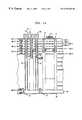
- FIG. 1is an exploded perspective view of the backplane of the invention
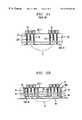
- FIG. 1Ais an elevational cross-sectional view of a portion of the backplane of FIG. 1;
- FIG. 2Ais a cross-section of a portion of the backplane without the use of a ground plane cap
- FIGS. 2B-2Eare cross-sectional views of a portion of the backplane showing different embodiments of the ground plane cap layer;
- FIG. 3Ais an elevational cross-section of one of the printed circuit layers of the backplane before modification to improve impedance matching and FIG. 3B shows the layer after modification;
- FIG. 4Ais an exploded perspective view of a portion of the backplane illustrating potential leakage paths between traces on a trace layer and FIG. 4B illustrates an arrangement for reducing the leakage of RF energy between the traces on the trace layer.
- the multi-layer backplane 10is shown respectively in an exploded perspective view and a cross-sectional view.
- the term “layer”is applied to a portion of the backplane that has electrically conductive material, such as copper, used as conductive traces for printed circuits and/or for electrical ground, e.g., ground plane, purposes.
- the backplane 10is illustratively described as adapted to be used with a cellular or PCS telephone station to perform various functions.
- These functionsinclude splitting, combining and distributing radio frequency (RF) signals from one or more receivers; supplying RF signals to be transmitted to one or more transmitters; processing such signals in one or more radio modules that are to be plugged into the backplane, and interfacing with external RF infrastructures, such as amplifiers, filters, and antennas.
- RFradio frequency
- the backplaneuses printed circuit media to convey the signals in a manner to minimize RF transmission losses through impedance matching and by minimizing the size of the backplane. This is done while maximizing isolation between the RF energy transmission paths.
- the backplaneeliminates the need for discrete cables and providing external connection between RF combining and splitting devices, thus reducing overall system cost and size.
- Backplane 10also has capabilities for conveying digital and analog signals, as well as for making connections for power supply.
- the backplanehas an uppermost combination surface trace and ground layer 20 T- 1 over a dielectric sheet 40 -D 1 which insulates the conductive material of layer 20 T- 1 from the next trace layer 20 T- 2 .
- the trace layer 20 T- 2is on a dielectric sheet 40 D 2 -A which electrically insulates it from an associated ground plane layer 44 G- 2 of electrically conductive material.
- the ground plane layer 44 G- 2is electrically insulated from the next trace layer 20 T- 3 by a dielectric sheet 40 D 2 -B.
- the trace layer 20 T- 2has its own respective ground plane layer 44 G- 2 and this ground plane layer is insulated from the next trace layer by a dielectric sheet 40 D 2 -B.
- the alternation of a trace layer 20 T, dielectric sheet 40 D-A, ground plane layer 44 G and dielectric sheet 44 D-Bcontinues to the bottom of the backplane in as many replications as required for the backplane.
- the backplaneis to have N trace layers, ending in the final ground plane layer 44 G-N for the last trace layer.
- ground plane layer 44 G-Nis separated by a dielectric sheet 48 covered by a final cap conductive ground plane layer 49 , whose function is described below.
- the ground plane cap layer 49is electrically connected by conductive vias 47 extending through the dielectric sheet 48 to make electrical connection with the lowermost trace layer ground plane 44 G-N, associated with a trace layer, as shown in FIGS. 1A, 2 C and 2 E.
- vias 91may be used which extend through the backplane and connect the cap layer 49 to all ground reference planes 44 of the backplane and to an electrical ground reference on the interface layer 20 T- 1 , as shown in FIGS. 2B and 2D.
- the upper layer 20 T- 1is for interface purposes and has a combination of traces and an electrical ground reference.
- the ground referenceis designated GND and is arrayed as part of layer 20 T- 1 , as required.
- Interface layer 20 T- 1provides access through connectors mounted to it and to other trace layers of the backplane to receive signals from or convey signals to traces on these other layers.
- trace layers 2 OT- 2 , 20 T- 3 and 20 T- 4handle RF signals and the remaining trace layers handle other signals, such as digital and analog, and provide connections to power supply functions.
- the RF signalsare confined to one section of the backplane.
- Other configurations of the layerscan be used as needed.
- the interface layer 20 T- 1has a plurality of coaxial connectors and various types of sockets, such as for providing connections to external circuit devices, and one or more surface mounted RF devices, such as a splitter. These are arranged in a pre-determined geometric pattern.
- Each of the coaxial connectorshas a single center pin and the device sockets have multiple pins which extend into the backplane until the respective pin comes into electrical contact with a predetermined trace of a predetermined layer to which the respective connector center pin or socket pin is to make electrical contact.
- the geometric pattern of the arrangement of these elementscorresponds to the traces on trace layers 20 T below the interface layer 20 T- 1 to which the pins are to be connected.
- FIG. 1there is illustratively shown on interface layer 20 T- 1 a first component row of four coaxial connectors 22 - 1 through 22 - 4 .
- Connector 22 - 1is to have a cable connected thereto which is to be ultimately connected to an external transmitter of radio frequency signals.
- the coaxial connectors 22 - 2 and 22 - 3are to have cables connected thereto from different receivers of radio frequency energy, while connector 22 - 4 is to have a cable connected to a reference signal frequency source which sets the timing for RF components of the backplane and for other purposes.
- those connectors associated with RF transmissionare designated Tx
- those which receive RF energyare designated Rx
- those with a reference frequency signalare designated as REF.
- Each of the coaxial connectors 22has a center pin which is to be electrically connected to a trace conductor of a selected printed circuit layer below interface layer 20 T- 1 .
- An RF combiner 23is shown as a surface mounted device. This has electrical terminals on layer 20 T- 1 (see FIG. 1A) to which contact is made from the traces of other layers, as shown in FIG. 1 A. It is also possible, if desired, to implement the circuit of some surface mounted RF devices by using a printed circuit pattern on a trace layer or layers.
- the next row of components on the interface layer 20 T- 1includes a group of sockets, or plugs, 26 which serve as pin fields for electrical connection with plugs or sockets of external circuits for performing any function, such as signal processing by a digital signal processor circuit.
- the rowillustratively has a second pin field socket 26 - 7 and is completed by a set 30 of five blind mate plug-in RF coaxial connectors which are to accept and interface with a plug-in radio module 38 . Two of the plug-in radio modules 38 are shown. These are standard packages and form no part of the present invention.
- blind mate plug-in connectors 30are shown, there being two each in the next two rows.
- the layout shownis only illustrative and there can be any configuration of coaxial connectors 22 , sockets 26 and sets of blind mate plug-in connectors 30 as needed and desired.
- each layer and dielectric sheethas holes through which each of the pins of the connectors and sockets pass without making electrical connection until they reach the trace layer having the trace to which electrical connection is to be made.
- the trace layer 20 T- 2in the illustrative example being described, is used to process signals by an RF splitter, which can be a surface mounted device that supplies RF signals to the external transmitters via the coaxial connectors 22 on the interface layer 20 T- 1 .
- Layer 20 T- 2is made by conventional printed circuit technology and has thereon a plurality of traces extending from an illustrative common trace 50 , which actually is the junction of a number of traces and connection traces that lead to surface mounted devices. As seen, for example, one of the traces 51 extends to a location aligned under the Tx coaxial connector 22 - 1 , so it can be connected to the center pin of this connector.
- traces 52 and 53 of layer 20 T- 2are positioned to have ends associated with other of the coaxial connectors of the interface layer.
- a dielectric layer 40 D 2 -Abelow that its associated ground plane layer 44 G- 2 .
- the next lower trace layer 20 T- 3is illustratively shown as used for processing RF signals relative to a receiving function.
- Layer 20 T- 3shows a common trace 60 which represents the junctions of a plurality of traces that perform combining and splitting functions, and from which connections can be made to the pins extending from the coaxial connectors 22 and 30 , and surface mounted devices on the interface layer 20 T- 1 which are associated with the receiver function.
- FIG. 1does not show trace layers below 20 T- 3 .
- Trace layer 20 T- 4shown in FIG. 1A, would have a trace pattern necessary to perform another RF signal function.
- the trace layers below 20 T- 4are used to perform different functions. For example, there are trace layers corresponding to the connections for the pins extending from the various sockets 26 - 1 . It is preferred that RF signals and other types of signals are not processed on the same layer. It is preferred that RF transmitter and receiver functions be divided and accommodated by different trace layers and associated ground planes so that transmitter and receiver RF signals are not processed in one trace layer where they could interfere with one another.
- FIG. 1Ashows one coaxial connector of the backplane, illustratively 22 - 1 for the transmitter function, that is mounted to the interface layer 20 T- 1 .
- Each of the connectors 22which can be of the press fit type, may be circular, or of any other suitable shape, and has an outer sleeve, or set of pins, 22 G used to mount the connector to the backplane.
- the connectoris grounded through a vertically extending circular channel, or set of channels, 39 that accepts the sleeve or pins 22 G of the connector body and extends though the backplane to the last ground plane layer 44 G-N.
- Each channel 39is electrically connected to each ground plane of the board from the interface layer, all intermediate ground plane layers 44 and to the last ground plane layer 44 G-N.
- the connector center pins 22 Care in plated-through holes 37 with connector center pin 22 C shown as being electrically connected to a trace of trace layer 20 T- 4 at C.
- the plated-through hole 37above and below trace layer 20 T- 4 , does not make electrical contact with a trace on any other layer.
- the end of connector center pin 22 Cis shown illustratively terminating somewhat below the ground plane layer 44 G- 4 of the last trace layer 20 T- 4 that handles RF signals.
- a center pincan have a length which terminates at any desired point.
- the portion of the plated-through hole 37 below the terminal end of connector center pin 22 C down to the last ground plane layer 44 G-Nis removed, such as by drilling, to remove the conductive plating. The reason for this is described below in connection with FIG. 3 .
- FIG. 1Aalso illustratively shows two transmission vias 71 and 72 extending vertically in the backplane. These are used to make connections between the surface mounted RF device 23 and certain traces for RF energy in the transmission path of a trace layer.
- the vias 71 and 72are through-holes plated, originally down to the bottom ground plane layer 44 G-N, and then the plating is removed, as shown by 73 , to a point below the trace layer on which electrical connection is made. The reason for this is described below. As shown in FIG.
- FIGS. 2A-2Ethe purpose of the ground plane cap layer 49 is now described.
- FIG. 2Ashows a prior art backplane without the cap layer 49 .
- the solid line Lthere is a leakage path for the RF energy from the center pins of the two coaxial connectors. This leakage is to be eliminated if possible.
- Such a leakage pathdoes not exist on the interface layer because of the isolation that each connector body provides for the signal at its respective center contact.
- FIGS. 2B-2Eshow the same portion of a backplane as in FIG. 2A but with the addition of the cap back plane layer 49 .
- the cap layer 49extends over the entire surface of dielectric sheet 48 .
- Each via 91electrically contacts each of the ground plane layers as it extends through the board. This closes off the leakage path between the center pins 22 C of the two adjacent connectors, as shown by the dashed line L. That is, the cap layer 49 isolates each connector and prevents leakage of RF energy between the connector center contacts.
- FIG. 2Ccorresponds to FIG. 1 A and the ground plane cap layer 49 overlies the entire dielectric sheet 48 .
- the vias 47do not extend completely through the board like vias 91 in FIG. 2 B. It may be more advantageous to have a via, such as 47 , that extends only partly through the board rather than a full depth via, such as 91 , since the holes for the vias are usually made after the multi-layer board is fully assembled. That is, it is easier to make a hole of lesser depth.
- FIG. 2Dthere are the full length vias 91 from the interface layer 20 T- 1 to the cap layer 49 , like in FIG. 2 B.
- the cap layer 49is in patches. That is, the cap layer is not co-extensive with the entire lower surface of the dielectric sheet 48 but is only on the areas overlying two adjacent coaxial connector center pins. This still serves to prevent RF energy leakage between the center pins of the two connectors.
- FIG. 2Ethe partial vias 47 are used as in FIG. 2 C.
- the difference here, like in FIG. 2D,is that there are only patches for the cap layer 49 instead of the full co-extensive layer as in FIG. 2 D.
- the desired result of blocking leakage of the RF energyis still obtained.
- the backplaneIt is desired to construct the backplane with impedances matched as closely as possible to various elements on the backplane and to cables of external circuits which are to be connected to the backplane.
- a portion of the backplaneis illustratively shown having two connectors 22 - 1 and 22 - 2 on the top layer 20 T- 1 as well as two surface mounted RF components, such as a combiner or splitter, 23 and 23 A.
- the center pin 22 C of each of the connectorsis shown in its plated hole 37 extending down to the last trace layer or the dielectric sheet above it.
- the portions of the conductive connector through holes 37 below the terminal ends of the center pins 22 C and the portions of the conductive transition vias 71 and 72 below the trace layer at which connection is made to the connector center pinalters the impedance of the connectors 22 and the respective RF device 23 and 23 A. This can be capacitive and/or inductive, but in most cases it is undesired.
- FIG. 3Bshows the same portion of the backplane of FIG. 3A in which the excess conductive material is removed from the connector center pin through-holes 37 , from the lowermost ground plane layer 44 G-N up to a point below the terminal ends of the center pins. It may also be removed through the dielectric 48 and the end cup 49 . This is shown by an enlargement 37 X of the through-hole.
- Such removal of the conductive materialmay be accomplished, for example, by drilling the backplane from the lowermost ground plane 44 G-N to the desired point before the dielectric layer 48 and cap layer 49 are attached. This is called “back drilling”.
- transition vias 71 and 72are back drilled at 71 X and 72 X to remove the conductive material up to a point below the trace layer it uses for making contact to the connector center pin. This removes the excess conductive material in the through-hole or via to eliminate its effect on the connector 22 or surface mounted RF device 23 .
- FIGS. 4A and 4Bshow the advantages of the use of vias to prevent leakage of RF energy between the traces of a trace layer carrying such energy.
- a portion of the backplaneis shown, this being the top layer 20 T- 1 , a dielectric sheet 40 D- 1 between the top layer and layer 20 T- 2 which handles RF energy, a dielectric sheet 40 D- 2 and a ground plane layer 44 G- 2 .
- the layer 20 T- 2as described with respect to FIGS. 1 and 1A, has traces 55 on which RF energy is flowing. As seen in FIG. 4A, and as shown by the arrows L, there is leakage between the traces. This can cause noise in and distortion of the signal.
- a stitch type pattern of a line of conductive vias 96is provided along each side of a trace 55 .
- the spacing of the viasis selected as a function of the wavelength ( ⁇ ) of the signal carried by the trace.
- the spacingcan be, for example, ⁇ / 20 .
- the vias 96are plated through holes and in FIG. 4B are shown extending from the top layer 20 T- 1 , where contact is made with a ground potential portion GND, and a ground plane layer below the trace layer 20 T- 2 , here 44 G- 2 . This isolates RF energy from leaking from a trace 55 since there is a ground reference running along each side of the trace.
- the requirementis that the lines of vias 96 are in electrical contact with each of the ground plane layers 44 above and below the trace 55 that is to be isolated. If desired, the vias 96 can extend either further up and/or down from the trace layer containing the trace 55 to be isolated.
- the lines of vias 96isolate one trace from another from the RF point of view, and thereby reduce or substantially eliminate leakage of RF energy between the traces.
- the via stitching, used in combination with the cap layer 49reduces RF energy leakage substantially throughout the backplane.
Landscapes
- Engineering & Computer Science (AREA)
- Microelectronics & Electronic Packaging (AREA)
- Physics & Mathematics (AREA)
- Electromagnetism (AREA)
- Production Of Multi-Layered Print Wiring Board (AREA)
Abstract
Description
Claims (18)
Priority Applications (1)
| Application Number | Priority Date | Filing Date | Title |
|---|---|---|---|
| US09/200,092US6392160B1 (en) | 1998-11-25 | 1998-11-25 | Backplane for radio frequency signals |
Applications Claiming Priority (1)
| Application Number | Priority Date | Filing Date | Title |
|---|---|---|---|
| US09/200,092US6392160B1 (en) | 1998-11-25 | 1998-11-25 | Backplane for radio frequency signals |
Publications (1)
| Publication Number | Publication Date |
|---|---|
| US6392160B1true US6392160B1 (en) | 2002-05-21 |
Family
ID=22740300
Family Applications (1)
| Application Number | Title | Priority Date | Filing Date |
|---|---|---|---|
| US09/200,092Expired - LifetimeUS6392160B1 (en) | 1998-11-25 | 1998-11-25 | Backplane for radio frequency signals |
Country Status (1)
| Country | Link |
|---|---|
| US (1) | US6392160B1 (en) |
Cited By (85)
| Publication number | Priority date | Publication date | Assignee | Title |
|---|---|---|---|---|
| US20020159238A1 (en)* | 2001-04-27 | 2002-10-31 | Kurt Gross | Mounting configuration of electric and/or electronic components on a printed circuit board |
| US6535397B2 (en)* | 2001-05-31 | 2003-03-18 | Harris Corporation | Interconnect structure for interconnecting electronic modules |
| US6574115B2 (en)* | 2000-10-26 | 2003-06-03 | International Business Machines Corporation | Computer system, electronic circuit board, and card |
| US6639154B1 (en)* | 2000-10-10 | 2003-10-28 | Teradyne, Inc. | Apparatus for forming a connection between a circuit board and a connector, having a signal launch |
| US20040008034A1 (en)* | 2002-07-09 | 2004-01-15 | Mastoris Steven F. | Testing device and method for testing backplanes and connectors on backplanes |
| US6700076B2 (en)* | 2000-09-28 | 2004-03-02 | Eic Corporation | Multi-layer interconnect module and method of interconnection |
| US6730859B2 (en)* | 2000-03-27 | 2004-05-04 | Shinko Electric Industries Co., Ltd. | Substrate for mounting electronic parts thereon and method of manufacturing same |
| US6759596B1 (en)* | 2000-05-12 | 2004-07-06 | Shipley Company | Sequential build circuit board |
| US6784376B1 (en)* | 2001-08-16 | 2004-08-31 | Amkor Technology, Inc. | Solderable injection-molded integrated circuit substrate and method therefor |
| US20050035825A1 (en)* | 2003-07-18 | 2005-02-17 | Carson James Crawford | Double-sided, edge-mounted stripline signal processing modules and modular network |
| US20050041398A1 (en)* | 2002-05-01 | 2005-02-24 | Huemoeller Ronald Patrick | Integrated circuit substrate having embedded back-side access conductors and vias |
| US6963209B1 (en)* | 2004-07-23 | 2005-11-08 | Teradyne, Inc. | Apparatus and method for calibrating equipment for high frequency measurements |
| US20060067067A1 (en)* | 2004-09-28 | 2006-03-30 | Teradyne, Inc. | Backplane with routing to reduce layer count |
| US20060071840A1 (en)* | 2004-09-15 | 2006-04-06 | Yu-Chiang Cheng | Circuit structure and circuit substrate for modifying charcteristic impedance by using different reference planes |
| US20060237222A1 (en)* | 2005-04-26 | 2006-10-26 | Eiichi Hosomi | Method and system for an improved package substrate for use with a semiconductor package |
| US20060243481A1 (en)* | 2005-05-02 | 2006-11-02 | Cisco Technology, Inc. (A California Corporation) | Apertures for signal shaping using ground and signal PTH back-drilling |
| US7145238B1 (en) | 2004-05-05 | 2006-12-05 | Amkor Technology, Inc. | Semiconductor package and substrate having multi-level vias |
| US20060278429A1 (en)* | 2003-09-19 | 2006-12-14 | Tourne Joseph A | Closed loop backdrilling system |
| US7185426B1 (en) | 2002-05-01 | 2007-03-06 | Amkor Technology, Inc. | Method of manufacturing a semiconductor package |
| US20080043447A1 (en)* | 2002-05-01 | 2008-02-21 | Amkor Technology, Inc. | Semiconductor package having laser-embedded terminals |
| US7334326B1 (en) | 2001-06-19 | 2008-02-26 | Amkor Technology, Inc. | Method for making an integrated circuit substrate having embedded passive components |
| US20080227311A1 (en)* | 2007-03-14 | 2008-09-18 | Jason Edward Chan | Adjacent plated through holes with staggered couplings for crosstalk reduction in high speed printed circuit boards |
| WO2009023238A1 (en)* | 2007-08-13 | 2009-02-19 | Force 10 Networks, Inc. | High-speed router with backplane using multi-diameter drilled thru-holes and vias |
| US7501338B1 (en) | 2001-06-19 | 2009-03-10 | Amkor Technology, Inc. | Semiconductor package substrate fabrication method |
| US7540744B1 (en) | 2008-01-08 | 2009-06-02 | Fci Americas Technology, Inc. | Shared hole orthogonal footprint with backdrilled vias |
| US7548430B1 (en) | 2002-05-01 | 2009-06-16 | Amkor Technology, Inc. | Buildup dielectric and metallization process and semiconductor package |
| US7550857B1 (en) | 2006-11-16 | 2009-06-23 | Amkor Technology, Inc. | Stacked redistribution layer (RDL) die assembly package |
| CN100512023C (en)* | 2006-05-18 | 2009-07-08 | 英业达股份有限公司 | High-speed signal transmission line with parallel and serial conductive connection posts |
| US7589398B1 (en) | 2006-10-04 | 2009-09-15 | Amkor Technology, Inc. | Embedded metal features structure |
| US7633765B1 (en) | 2004-03-23 | 2009-12-15 | Amkor Technology, Inc. | Semiconductor package including a top-surface metal layer for implementing circuit features |
| US7670962B2 (en) | 2002-05-01 | 2010-03-02 | Amkor Technology, Inc. | Substrate having stiffener fabrication method |
| EP1863326A4 (en)* | 2005-03-23 | 2010-03-31 | Fujitsu Ltd | PRINTED CIRCUIT BOARD |
| US7750250B1 (en) | 2006-12-22 | 2010-07-06 | Amkor Technology, Inc. | Blind via capture pad structure |
| US7752752B1 (en) | 2007-01-09 | 2010-07-13 | Amkor Technology, Inc. | Method of fabricating an embedded circuit pattern |
| US20110080187A1 (en)* | 2009-10-02 | 2011-04-07 | Peter Hotz | Device Interface Board with Cavity Back for Very High Frequency Applications |
| US7960827B1 (en) | 2009-04-09 | 2011-06-14 | Amkor Technology, Inc. | Thermal via heat spreader package and method |
| WO2011088308A1 (en)* | 2010-01-18 | 2011-07-21 | 3M Innovative Properties Company | Contact pin holder |
| US20110240348A1 (en)* | 2010-03-31 | 2011-10-06 | Flextronics Ap, Llc | Backdrilling of multilayer printed circuit boards |
| US8222538B1 (en) | 2009-06-12 | 2012-07-17 | Amkor Technology, Inc. | Stackable via package and method |
| US8294276B1 (en) | 2010-05-27 | 2012-10-23 | Amkor Technology, Inc. | Semiconductor device and fabricating method thereof |
| US8300423B1 (en) | 2010-05-25 | 2012-10-30 | Amkor Technology, Inc. | Stackable treated via package and method |
| US20120279774A1 (en)* | 2009-11-27 | 2012-11-08 | Bae Systems Plc | Circuit board |
| US8323771B1 (en) | 2007-08-15 | 2012-12-04 | Amkor Technology, Inc. | Straight conductor blind via capture pad structure and fabrication method |
| US8337657B1 (en) | 2010-10-27 | 2012-12-25 | Amkor Technology, Inc. | Mechanical tape separation package and method |
| US8338229B1 (en) | 2010-07-30 | 2012-12-25 | Amkor Technology, Inc. | Stackable plasma cleaned via package and method |
| CN103025082A (en)* | 2011-09-21 | 2013-04-03 | 英业达股份有限公司 | Method for manufacturing printed circuit board and printed circuit board structure |
| US8471154B1 (en) | 2009-08-06 | 2013-06-25 | Amkor Technology, Inc. | Stackable variable height via package and method |
| US8482134B1 (en) | 2010-11-01 | 2013-07-09 | Amkor Technology, Inc. | Stackable package and method |
| US8525318B1 (en) | 2010-11-10 | 2013-09-03 | Amkor Technology, Inc. | Semiconductor device and fabricating method thereof |
| US8536462B1 (en) | 2010-01-22 | 2013-09-17 | Amkor Technology, Inc. | Flex circuit package and method |
| US8535961B1 (en) | 2010-12-09 | 2013-09-17 | Amkor Technology, Inc. | Light emitting diode (LED) package and method |
| US8557629B1 (en) | 2010-12-03 | 2013-10-15 | Amkor Technology, Inc. | Semiconductor device having overlapped via apertures |
| US8623753B1 (en) | 2009-05-28 | 2014-01-07 | Amkor Technology, Inc. | Stackable protruding via package and method |
| US8633598B1 (en) | 2011-09-20 | 2014-01-21 | Amkor Technology, Inc. | Underfill contacting stacking balls package fabrication method and structure |
| US8653674B1 (en) | 2011-09-15 | 2014-02-18 | Amkor Technology, Inc. | Electronic component package fabrication method and structure |
| US8717775B1 (en) | 2010-08-02 | 2014-05-06 | Amkor Technology, Inc. | Fingerprint sensor package and method |
| US8796561B1 (en) | 2009-10-05 | 2014-08-05 | Amkor Technology, Inc. | Fan out build up substrate stackable package and method |
| US8826531B1 (en) | 2005-04-05 | 2014-09-09 | Amkor Technology, Inc. | Method for making an integrated circuit substrate having laminated laser-embedded circuit layers |
| US8872329B1 (en) | 2009-01-09 | 2014-10-28 | Amkor Technology, Inc. | Extended landing pad substrate package structure and method |
| US8890329B2 (en) | 2011-04-26 | 2014-11-18 | Amkor Technology, Inc. | Semiconductor device |
| US8937381B1 (en) | 2009-12-03 | 2015-01-20 | Amkor Technology, Inc. | Thin stackable package and method |
| US9013011B1 (en) | 2011-03-11 | 2015-04-21 | Amkor Technology, Inc. | Stacked and staggered die MEMS package and method |
| US9029962B1 (en) | 2011-10-12 | 2015-05-12 | Amkor Technology, Inc. | Molded cavity substrate MEMS package fabrication method and structure |
| US9202783B1 (en)* | 2011-03-24 | 2015-12-01 | Juniper Networks, Inc. | Selective antipad backdrilling for printed circuit boards |
| US20150348901A1 (en)* | 2014-05-27 | 2015-12-03 | R&D Circuits, Inc | Structure for Isolating High Speed Digital Signals in a High Density Grid Array |
| US9391043B2 (en) | 2012-11-20 | 2016-07-12 | Amkor Technology, Inc. | Semiconductor device and manufacturing method thereof |
| TWI563753B (en)* | 2011-02-04 | 2016-12-21 | 3M Innovative Properties Co | Ic device socket |
| US9543242B1 (en) | 2013-01-29 | 2017-01-10 | Amkor Technology, Inc. | Semiconductor package and fabricating method thereof |
| US9691734B1 (en) | 2009-12-07 | 2017-06-27 | Amkor Technology, Inc. | Method of forming a plurality of electronic component packages |
| US9691635B1 (en) | 2002-05-01 | 2017-06-27 | Amkor Technology, Inc. | Buildup dielectric layer having metallization pattern semiconductor package fabrication method |
| US9704747B2 (en) | 2013-03-29 | 2017-07-11 | Amkor Technology, Inc. | Semiconductor device and manufacturing method thereof |
| US9704842B2 (en) | 2013-11-04 | 2017-07-11 | Amkor Technology, Inc. | Interposer, manufacturing method thereof, semiconductor package using the same, and method for fabricating the semiconductor package |
| US9721872B1 (en) | 2011-02-18 | 2017-08-01 | Amkor Technology, Inc. | Methods and structures for increasing the allowable die size in TMV packages |
| US9748154B1 (en) | 2010-11-04 | 2017-08-29 | Amkor Technology, Inc. | Wafer level fan out semiconductor device and manufacturing method thereof |
| US9820403B2 (en) | 2015-12-08 | 2017-11-14 | Ciena Corporation | Backplane alignment and stiffening apparatus for two backplanes spanning single modules |
| US9907156B1 (en)* | 2015-03-06 | 2018-02-27 | Juniper Networks, Inc. | Cross-talk reduction for high speed signaling at ball grid array region and connector region |
| TWI620936B (en)* | 2017-02-22 | 2018-04-11 | 中華精測科技股份有限公司 | Testing probe card for integrated circuit |
| US9960328B2 (en) | 2016-09-06 | 2018-05-01 | Amkor Technology, Inc. | Semiconductor device and manufacturing method thereof |
| US10188011B2 (en) | 2015-12-02 | 2019-01-22 | Ciena Corporation | Offloaded backplane for power distribution in high-speed data applications |
| US10811277B2 (en) | 2004-03-23 | 2020-10-20 | Amkor Technology, Inc. | Encapsulated semiconductor package |
| US11081370B2 (en) | 2004-03-23 | 2021-08-03 | Amkor Technology Singapore Holding Pte. Ltd. | Methods of manufacturing an encapsulated semiconductor device |
| CN113597100A (en)* | 2021-06-23 | 2021-11-02 | 浪潮电子信息产业股份有限公司 | Method, circuit board, equipment and storage medium for optimizing differential via impedance |
| US11350520B2 (en)* | 2019-08-08 | 2022-05-31 | At&S Austria Technologie & Systemtechnik Aktiengesellschaft | Component carrier and method of manufacturing the same |
| US20220369468A1 (en)* | 2014-11-06 | 2022-11-17 | Semiconductor Components Industries, Llc | Substrate structures and methods of manufacture |
| US20240057253A1 (en)* | 2020-12-16 | 2024-02-15 | Lg Innotek Co., Ltd. | Circuit board |
Citations (6)
| Publication number | Priority date | Publication date | Assignee | Title |
|---|---|---|---|---|
| US4904968A (en)* | 1989-04-07 | 1990-02-27 | Tektronix, Inc. | Circuit board configuration for reducing signal distortion |
| JPH02281699A (en)* | 1989-04-21 | 1990-11-19 | Kokusai Electric Co Ltd | multilayer wiring circuit board |
| US5199879A (en)* | 1992-02-24 | 1993-04-06 | International Business Machines Corporation | Electrical assembly with flexible circuit |
| US5308250A (en)* | 1992-10-30 | 1994-05-03 | Hewlett-Packard Company | Pressure contact for connecting a coaxial shield to a microstrip ground plane |
| US5641294A (en)* | 1995-05-31 | 1997-06-24 | Northern Telecom Limited | Backplane assembly including coaxial connectors |
| US6239385B1 (en)* | 1998-02-27 | 2001-05-29 | Agilent Technologies, Inc. | Surface mountable coaxial solder interconnect and method |
- 1998
- 1998-11-25USUS09/200,092patent/US6392160B1/ennot_activeExpired - Lifetime
Patent Citations (6)
| Publication number | Priority date | Publication date | Assignee | Title |
|---|---|---|---|---|
| US4904968A (en)* | 1989-04-07 | 1990-02-27 | Tektronix, Inc. | Circuit board configuration for reducing signal distortion |
| JPH02281699A (en)* | 1989-04-21 | 1990-11-19 | Kokusai Electric Co Ltd | multilayer wiring circuit board |
| US5199879A (en)* | 1992-02-24 | 1993-04-06 | International Business Machines Corporation | Electrical assembly with flexible circuit |
| US5308250A (en)* | 1992-10-30 | 1994-05-03 | Hewlett-Packard Company | Pressure contact for connecting a coaxial shield to a microstrip ground plane |
| US5641294A (en)* | 1995-05-31 | 1997-06-24 | Northern Telecom Limited | Backplane assembly including coaxial connectors |
| US6239385B1 (en)* | 1998-02-27 | 2001-05-29 | Agilent Technologies, Inc. | Surface mountable coaxial solder interconnect and method |
Cited By (166)
| Publication number | Priority date | Publication date | Assignee | Title |
|---|---|---|---|---|
| US6730859B2 (en)* | 2000-03-27 | 2004-05-04 | Shinko Electric Industries Co., Ltd. | Substrate for mounting electronic parts thereon and method of manufacturing same |
| US6759596B1 (en)* | 2000-05-12 | 2004-07-06 | Shipley Company | Sequential build circuit board |
| US6700076B2 (en)* | 2000-09-28 | 2004-03-02 | Eic Corporation | Multi-layer interconnect module and method of interconnection |
| US6639154B1 (en)* | 2000-10-10 | 2003-10-28 | Teradyne, Inc. | Apparatus for forming a connection between a circuit board and a connector, having a signal launch |
| US6574115B2 (en)* | 2000-10-26 | 2003-06-03 | International Business Machines Corporation | Computer system, electronic circuit board, and card |
| US20020159238A1 (en)* | 2001-04-27 | 2002-10-31 | Kurt Gross | Mounting configuration of electric and/or electronic components on a printed circuit board |
| US6723926B2 (en)* | 2001-04-27 | 2004-04-20 | Siemens Aktiengesellschaft | Mounting configuration of electric and/or electronic components on a printed circuit board |
| US6535397B2 (en)* | 2001-05-31 | 2003-03-18 | Harris Corporation | Interconnect structure for interconnecting electronic modules |
| US7501338B1 (en) | 2001-06-19 | 2009-03-10 | Amkor Technology, Inc. | Semiconductor package substrate fabrication method |
| US7334326B1 (en) | 2001-06-19 | 2008-02-26 | Amkor Technology, Inc. | Method for making an integrated circuit substrate having embedded passive components |
| US6784376B1 (en)* | 2001-08-16 | 2004-08-31 | Amkor Technology, Inc. | Solderable injection-molded integrated circuit substrate and method therefor |
| US9691635B1 (en) | 2002-05-01 | 2017-06-27 | Amkor Technology, Inc. | Buildup dielectric layer having metallization pattern semiconductor package fabrication method |
| US20080043447A1 (en)* | 2002-05-01 | 2008-02-21 | Amkor Technology, Inc. | Semiconductor package having laser-embedded terminals |
| US7670962B2 (en) | 2002-05-01 | 2010-03-02 | Amkor Technology, Inc. | Substrate having stiffener fabrication method |
| US7548430B1 (en) | 2002-05-01 | 2009-06-16 | Amkor Technology, Inc. | Buildup dielectric and metallization process and semiconductor package |
| US8026587B1 (en) | 2002-05-01 | 2011-09-27 | Amkor Technology, Inc. | Semiconductor package including top-surface terminals for mounting another semiconductor package |
| US8316536B1 (en) | 2002-05-01 | 2012-11-27 | Amkor Technology, Inc. | Multi-level circuit substrate fabrication method |
| US10461006B1 (en) | 2002-05-01 | 2019-10-29 | Amkor Technology, Inc. | Encapsulated semiconductor package |
| US8322030B1 (en)* | 2002-05-01 | 2012-12-04 | Amkor Technology, Inc. | Circuit-on-foil process for manufacturing a laminated semiconductor package substrate having embedded conductive patterns |
| US9812386B1 (en) | 2002-05-01 | 2017-11-07 | Amkor Technology, Inc. | Encapsulated semiconductor package |
| US8341835B1 (en) | 2002-05-01 | 2013-01-01 | Amkor Technology, Inc. | Buildup dielectric layer having metallization pattern semiconductor package fabrication method |
| US7671457B1 (en) | 2002-05-01 | 2010-03-02 | Amkor Technology, Inc. | Semiconductor package including top-surface terminals for mounting another semiconductor package |
| US7399661B2 (en) | 2002-05-01 | 2008-07-15 | Amkor Technology, Inc. | Method for making an integrated circuit substrate having embedded back-side access conductors and vias |
| US20050041398A1 (en)* | 2002-05-01 | 2005-02-24 | Huemoeller Ronald Patrick | Integrated circuit substrate having embedded back-side access conductors and vias |
| US7185426B1 (en) | 2002-05-01 | 2007-03-06 | Amkor Technology, Inc. | Method of manufacturing a semiconductor package |
| US8110909B1 (en) | 2002-05-01 | 2012-02-07 | Amkor Technology, Inc. | Semiconductor package including top-surface terminals for mounting another semiconductor package |
| US7297562B1 (en) | 2002-05-01 | 2007-11-20 | Amkor Technology, Inc. | Circuit-on-foil process for manufacturing a laminated semiconductor package substrate having embedded conductive patterns |
| US7312103B1 (en) | 2002-05-01 | 2007-12-25 | Amkor Technology, Inc. | Method for making an integrated circuit substrate having laser-embedded conductive patterns |
| US20040008034A1 (en)* | 2002-07-09 | 2004-01-15 | Mastoris Steven F. | Testing device and method for testing backplanes and connectors on backplanes |
| US6956379B2 (en)* | 2002-07-09 | 2005-10-18 | Hewlett-Packard Development Company, L.P. | Testing device and method for testing backplanes and connectors on backplanes |
| US20050035825A1 (en)* | 2003-07-18 | 2005-02-17 | Carson James Crawford | Double-sided, edge-mounted stripline signal processing modules and modular network |
| US6965279B2 (en)* | 2003-07-18 | 2005-11-15 | Ems Technologies, Inc. | Double-sided, edge-mounted stripline signal processing modules and modular network |
| US20050168301A1 (en)* | 2003-07-18 | 2005-08-04 | Carson James C. | Double-sided, edge-mounted stripline signal processing modules and modular network |
| US20060278429A1 (en)* | 2003-09-19 | 2006-12-14 | Tourne Joseph A | Closed loop backdrilling system |
| EP1663569A4 (en)* | 2003-09-19 | 2009-04-15 | Viasystems Group Inc | Closed loop backdrilling system |
| US8227338B1 (en) | 2004-03-23 | 2012-07-24 | Amkor Technology, Inc. | Semiconductor package including a top-surface metal layer for implementing circuit features |
| US10811277B2 (en) | 2004-03-23 | 2020-10-20 | Amkor Technology, Inc. | Encapsulated semiconductor package |
| US8018068B1 (en) | 2004-03-23 | 2011-09-13 | Amkor Technology, Inc. | Semiconductor package including a top-surface metal layer for implementing circuit features |
| US11081370B2 (en) | 2004-03-23 | 2021-08-03 | Amkor Technology Singapore Holding Pte. Ltd. | Methods of manufacturing an encapsulated semiconductor device |
| US11094560B1 (en) | 2004-03-23 | 2021-08-17 | Amkor Technology Singapore Holding Pte. Ltd. | Encapsulated semiconductor package |
| US7633765B1 (en) | 2004-03-23 | 2009-12-15 | Amkor Technology, Inc. | Semiconductor package including a top-surface metal layer for implementing circuit features |
| US7145238B1 (en) | 2004-05-05 | 2006-12-05 | Amkor Technology, Inc. | Semiconductor package and substrate having multi-level vias |
| US7365006B1 (en) | 2004-05-05 | 2008-04-29 | Amkor Technology, Inc. | Semiconductor package and substrate having multi-level vias fabrication method |
| US6963209B1 (en)* | 2004-07-23 | 2005-11-08 | Teradyne, Inc. | Apparatus and method for calibrating equipment for high frequency measurements |
| US20060071840A1 (en)* | 2004-09-15 | 2006-04-06 | Yu-Chiang Cheng | Circuit structure and circuit substrate for modifying charcteristic impedance by using different reference planes |
| US20060067067A1 (en)* | 2004-09-28 | 2006-03-30 | Teradyne, Inc. | Backplane with routing to reduce layer count |
| US7359214B2 (en)* | 2004-09-28 | 2008-04-15 | Amphenol Corporation | Backplane with routing to reduce layer count |
| EP1863326A4 (en)* | 2005-03-23 | 2010-03-31 | Fujitsu Ltd | PRINTED CIRCUIT BOARD |
| US8826531B1 (en) | 2005-04-05 | 2014-09-09 | Amkor Technology, Inc. | Method for making an integrated circuit substrate having laminated laser-embedded circuit layers |
| US20060237222A1 (en)* | 2005-04-26 | 2006-10-26 | Eiichi Hosomi | Method and system for an improved package substrate for use with a semiconductor package |
| US7531751B2 (en)* | 2005-04-26 | 2009-05-12 | Kabushiki Kaisha Toshiba | Method and system for an improved package substrate for use with a semiconductor package |
| EP1878328A4 (en)* | 2005-05-02 | 2011-08-03 | Cisco Tech Inc | Apertures for signal shaping using ground and signal pth back-drilling |
| US7291790B2 (en)* | 2005-05-02 | 2007-11-06 | Cisco Technology, Inc. | Apertures for signal shaping using ground and signal PTH back-drilling |
| CN101151945B (en)* | 2005-05-02 | 2010-12-22 | 思科技术公司 | Apertures for signal shaping using ground and signal PTH back-drilling |
| US20060243481A1 (en)* | 2005-05-02 | 2006-11-02 | Cisco Technology, Inc. (A California Corporation) | Apertures for signal shaping using ground and signal PTH back-drilling |
| WO2006118908A2 (en) | 2005-05-02 | 2006-11-09 | Cisco Technology, Inc. | Apertures for signal shaping using ground and signal pth back-drilling |
| WO2006118908A3 (en)* | 2005-05-02 | 2007-02-01 | Cisco Tech Inc | Apertures for signal shaping using ground and signal pth back-drilling |
| CN100512023C (en)* | 2006-05-18 | 2009-07-08 | 英业达股份有限公司 | High-speed signal transmission line with parallel and serial conductive connection posts |
| US11848214B2 (en) | 2006-08-01 | 2023-12-19 | Amkor Technology Singapore Holding Pte. Ltd. | Encapsulated semiconductor package |
| US7589398B1 (en) | 2006-10-04 | 2009-09-15 | Amkor Technology, Inc. | Embedded metal features structure |
| US7911037B1 (en) | 2006-10-04 | 2011-03-22 | Amkor Technology, Inc. | Method and structure for creating embedded metal features |
| US7825520B1 (en) | 2006-11-16 | 2010-11-02 | Amkor Technology, Inc. | Stacked redistribution layer (RDL) die assembly package |
| US7550857B1 (en) | 2006-11-16 | 2009-06-23 | Amkor Technology, Inc. | Stacked redistribution layer (RDL) die assembly package |
| US8203203B1 (en) | 2006-11-16 | 2012-06-19 | Amkor Technology, Inc. | Stacked redistribution layer (RDL) die assembly package |
| US8629546B1 (en) | 2006-11-16 | 2014-01-14 | Amkor Technology, Inc. | Stacked redistribution layer (RDL) die assembly package |
| US8671565B1 (en) | 2006-12-22 | 2014-03-18 | Amkor Technology, Inc. | Blind via capture pad structure fabrication method |
| US7750250B1 (en) | 2006-12-22 | 2010-07-06 | Amkor Technology, Inc. | Blind via capture pad structure |
| US7752752B1 (en) | 2007-01-09 | 2010-07-13 | Amkor Technology, Inc. | Method of fabricating an embedded circuit pattern |
| US7999192B2 (en)* | 2007-03-14 | 2011-08-16 | Amphenol Corporation | Adjacent plated through holes with staggered couplings for crosstalk reduction in high speed printed circuit boards |
| US20080227311A1 (en)* | 2007-03-14 | 2008-09-18 | Jason Edward Chan | Adjacent plated through holes with staggered couplings for crosstalk reduction in high speed printed circuit boards |
| US8481866B2 (en) | 2007-03-14 | 2013-07-09 | Amphenol Corporation | Adjacent plated through holes with staggered couplings for crosstalk reduction in high speed printed circuit boards |
| US9560774B2 (en)* | 2007-08-13 | 2017-01-31 | Force10 Networks, Inc. | Method of fabricating a circuit board |
| US20090045889A1 (en)* | 2007-08-13 | 2009-02-19 | Force 10 Networks, Inc. | High-speed router with backplane using muli-diameter drilled thru-holes and vias |
| WO2009023238A1 (en)* | 2007-08-13 | 2009-02-19 | Force 10 Networks, Inc. | High-speed router with backplane using multi-diameter drilled thru-holes and vias |
| TWI462656B (en)* | 2007-08-13 | 2014-11-21 | Force10 Networks Inc | High-speed router with backplane using multi-diameter drilled thru-holes and vias |
| US20120167386A1 (en)* | 2007-08-13 | 2012-07-05 | Dell Products L.P. | High-speed router with backplane using multi-diameter drilled thru-holes and vias |
| US8158892B2 (en)* | 2007-08-13 | 2012-04-17 | Force10 Networks, Inc. | High-speed router with backplane using muli-diameter drilled thru-holes and vias |
| US8323771B1 (en) | 2007-08-15 | 2012-12-04 | Amkor Technology, Inc. | Straight conductor blind via capture pad structure and fabrication method |
| US7540744B1 (en) | 2008-01-08 | 2009-06-02 | Fci Americas Technology, Inc. | Shared hole orthogonal footprint with backdrilled vias |
| US8872329B1 (en) | 2009-01-09 | 2014-10-28 | Amkor Technology, Inc. | Extended landing pad substrate package structure and method |
| US9462704B1 (en) | 2009-01-09 | 2016-10-04 | Amkor Technology, Inc. | Extended landing pad substrate package structure and method |
| US7960827B1 (en) | 2009-04-09 | 2011-06-14 | Amkor Technology, Inc. | Thermal via heat spreader package and method |
| US8623753B1 (en) | 2009-05-28 | 2014-01-07 | Amkor Technology, Inc. | Stackable protruding via package and method |
| US10206285B1 (en) | 2009-06-12 | 2019-02-12 | Amkor Technology, Inc. | Stackable via package and method |
| US11700692B2 (en) | 2009-06-12 | 2023-07-11 | Amkor Technology Singapore Holding Pte. Ltd. | Stackable via package and method |
| US10548221B1 (en) | 2009-06-12 | 2020-01-28 | Amkor Technology, Inc. | Stackable via package and method |
| US9012789B1 (en) | 2009-06-12 | 2015-04-21 | Amkor Technology, Inc. | Stackable via package and method |
| US12035472B2 (en) | 2009-06-12 | 2024-07-09 | Amkor Technology Singapore Holding Ptd. Ltd. | Stackable via package and method |
| US11089685B2 (en) | 2009-06-12 | 2021-08-10 | Amkor Technology Singapore Holding Pte. Ltd. | Stackable via package and method |
| US8222538B1 (en) | 2009-06-12 | 2012-07-17 | Amkor Technology, Inc. | Stackable via package and method |
| US9730327B1 (en) | 2009-06-12 | 2017-08-08 | Amkor Technology, Inc. | Stackable via package and method |
| US8704368B1 (en) | 2009-06-12 | 2014-04-22 | Amkor Technology, Inc. | Stackable via package and method |
| US10034372B1 (en) | 2009-06-12 | 2018-07-24 | Amkor Technology, Inc. | Stackable via package and method |
| US8471154B1 (en) | 2009-08-06 | 2013-06-25 | Amkor Technology, Inc. | Stackable variable height via package and method |
| US10257942B1 (en) | 2009-08-06 | 2019-04-09 | Amkor Technology, Inc. | Stackable variable height via package and method |
| US20110080187A1 (en)* | 2009-10-02 | 2011-04-07 | Peter Hotz | Device Interface Board with Cavity Back for Very High Frequency Applications |
| US8461855B2 (en) | 2009-10-02 | 2013-06-11 | Teradyne, Inc. | Device interface board with cavity back for very high frequency applications |
| US8796561B1 (en) | 2009-10-05 | 2014-08-05 | Amkor Technology, Inc. | Fan out build up substrate stackable package and method |
| US20120279774A1 (en)* | 2009-11-27 | 2012-11-08 | Bae Systems Plc | Circuit board |
| US8937381B1 (en) | 2009-12-03 | 2015-01-20 | Amkor Technology, Inc. | Thin stackable package and method |
| US9691734B1 (en) | 2009-12-07 | 2017-06-27 | Amkor Technology, Inc. | Method of forming a plurality of electronic component packages |
| US10546833B2 (en) | 2009-12-07 | 2020-01-28 | Amkor Technology, Inc. | Method of forming a plurality of electronic component packages |
| WO2011088308A1 (en)* | 2010-01-18 | 2011-07-21 | 3M Innovative Properties Company | Contact pin holder |
| US8536462B1 (en) | 2010-01-22 | 2013-09-17 | Amkor Technology, Inc. | Flex circuit package and method |
| US8302301B2 (en)* | 2010-03-31 | 2012-11-06 | Flextronics Ap, Llc | Method for backdrilling via stubs of multilayer printed circuit boards with reduced backdrill diameters |
| US20110240348A1 (en)* | 2010-03-31 | 2011-10-06 | Flextronics Ap, Llc | Backdrilling of multilayer printed circuit boards |
| US8300423B1 (en) | 2010-05-25 | 2012-10-30 | Amkor Technology, Inc. | Stackable treated via package and method |
| US8294276B1 (en) | 2010-05-27 | 2012-10-23 | Amkor Technology, Inc. | Semiconductor device and fabricating method thereof |
| US8338229B1 (en) | 2010-07-30 | 2012-12-25 | Amkor Technology, Inc. | Stackable plasma cleaned via package and method |
| US8717775B1 (en) | 2010-08-02 | 2014-05-06 | Amkor Technology, Inc. | Fingerprint sensor package and method |
| US8337657B1 (en) | 2010-10-27 | 2012-12-25 | Amkor Technology, Inc. | Mechanical tape separation package and method |
| US8753730B1 (en) | 2010-10-27 | 2014-06-17 | Amkor Technology, Inc. | Mechanical tape separation package |
| US8482134B1 (en) | 2010-11-01 | 2013-07-09 | Amkor Technology, Inc. | Stackable package and method |
| US9496210B1 (en) | 2010-11-01 | 2016-11-15 | Amkor Technology, Inc. | Stackable package and method |
| US12009343B1 (en) | 2010-11-01 | 2024-06-11 | Amkor Technology Singapore Holding Pte. Ltd. | Stackable package and method |
| US10903181B2 (en) | 2010-11-04 | 2021-01-26 | Amkor Technology Singapore Holding Pte. Ltd. | Wafer level fan out semiconductor device and manufacturing method thereof |
| US11855023B2 (en) | 2010-11-04 | 2023-12-26 | Amkor Technology Singapore Holding Pte. Ltd. | Wafer level fan out semiconductor device and manufacturing method thereof |
| US9748154B1 (en) | 2010-11-04 | 2017-08-29 | Amkor Technology, Inc. | Wafer level fan out semiconductor device and manufacturing method thereof |
| US8525318B1 (en) | 2010-11-10 | 2013-09-03 | Amkor Technology, Inc. | Semiconductor device and fabricating method thereof |
| US9177932B1 (en) | 2010-12-03 | 2015-11-03 | Amkor Technology, Inc. | Semiconductor device having overlapped via apertures |
| US8557629B1 (en) | 2010-12-03 | 2013-10-15 | Amkor Technology, Inc. | Semiconductor device having overlapped via apertures |
| US9837331B1 (en) | 2010-12-03 | 2017-12-05 | Amkor Technology, Inc. | Semiconductor device having overlapped via apertures |
| US8535961B1 (en) | 2010-12-09 | 2013-09-17 | Amkor Technology, Inc. | Light emitting diode (LED) package and method |
| TWI563753B (en)* | 2011-02-04 | 2016-12-21 | 3M Innovative Properties Co | Ic device socket |
| US11488892B2 (en) | 2011-02-18 | 2022-11-01 | Amkor Technology Singapore Holding Pte. Ltd. | Methods and structures for increasing the allowable die size in TMV packages |
| US10347562B1 (en) | 2011-02-18 | 2019-07-09 | Amkor Technology, Inc. | Methods and structures for increasing the allowable die size in TMV packages |
| US9721872B1 (en) | 2011-02-18 | 2017-08-01 | Amkor Technology, Inc. | Methods and structures for increasing the allowable die size in TMV packages |
| US9013011B1 (en) | 2011-03-11 | 2015-04-21 | Amkor Technology, Inc. | Stacked and staggered die MEMS package and method |
| US9202783B1 (en)* | 2011-03-24 | 2015-12-01 | Juniper Networks, Inc. | Selective antipad backdrilling for printed circuit boards |
| US8890329B2 (en) | 2011-04-26 | 2014-11-18 | Amkor Technology, Inc. | Semiconductor device |
| US8653674B1 (en) | 2011-09-15 | 2014-02-18 | Amkor Technology, Inc. | Electronic component package fabrication method and structure |
| US8941250B1 (en) | 2011-09-15 | 2015-01-27 | Amkor Technology, Inc. | Electronic component package fabrication method and structure |
| US8890337B1 (en) | 2011-09-20 | 2014-11-18 | Amkor Technology, Inc. | Column and stacking balls package fabrication method and structure |
| US8633598B1 (en) | 2011-09-20 | 2014-01-21 | Amkor Technology, Inc. | Underfill contacting stacking balls package fabrication method and structure |
| CN103025082B (en)* | 2011-09-21 | 2015-08-05 | 英业达股份有限公司 | A method of manufacturing a printed circuit board and a printed circuit board structure |
| CN103025082A (en)* | 2011-09-21 | 2013-04-03 | 英业达股份有限公司 | Method for manufacturing printed circuit board and printed circuit board structure |
| US9029962B1 (en) | 2011-10-12 | 2015-05-12 | Amkor Technology, Inc. | Molded cavity substrate MEMS package fabrication method and structure |
| US11527496B2 (en) | 2012-11-20 | 2022-12-13 | Amkor Technology Singapore Holding Pte. Ltd. | Semiconductor device comprising semiconductor die and interposer and manufacturing method thereof |
| US9728514B2 (en) | 2012-11-20 | 2017-08-08 | Amkor Technology, Inc. | Semiconductor device and manufacturing method thereof |
| US10679952B2 (en) | 2012-11-20 | 2020-06-09 | Amkor Technology, Inc. | Semiconductor device having an encapsulated front side and interposer and manufacturing method thereof |
| US9391043B2 (en) | 2012-11-20 | 2016-07-12 | Amkor Technology, Inc. | Semiconductor device and manufacturing method thereof |
| US9852976B2 (en) | 2013-01-29 | 2017-12-26 | Amkor Technology, Inc. | Semiconductor package and fabricating method thereof |
| US9543242B1 (en) | 2013-01-29 | 2017-01-10 | Amkor Technology, Inc. | Semiconductor package and fabricating method thereof |
| US9704747B2 (en) | 2013-03-29 | 2017-07-11 | Amkor Technology, Inc. | Semiconductor device and manufacturing method thereof |
| US9704842B2 (en) | 2013-11-04 | 2017-07-11 | Amkor Technology, Inc. | Interposer, manufacturing method thereof, semiconductor package using the same, and method for fabricating the semiconductor package |
| US11652038B2 (en) | 2013-11-19 | 2023-05-16 | Amkor Technology Singapore Holding Pte. Ltd. | Semiconductor package with front side and back side redistribution structures and fabricating method thereof |
| US12159823B2 (en) | 2013-11-19 | 2024-12-03 | Amkor Technology Singapore Holding Pte. Ltd. | Semiconductor package with front side and back side redistribution structures and fabricating method thereof |
| US10192816B2 (en) | 2013-11-19 | 2019-01-29 | Amkor Technology, Inc. | Semiconductor package and fabricating method thereof |
| US10943858B2 (en) | 2013-11-19 | 2021-03-09 | Amkor Technology Singapore Holding Pte. Ltd. | Semiconductor package and fabricating method thereof |
| US10079202B2 (en)* | 2014-05-27 | 2018-09-18 | R&D Circuits, Inc. | Structure for isolating high speed digital signals in a high density grid array |
| US20150348901A1 (en)* | 2014-05-27 | 2015-12-03 | R&D Circuits, Inc | Structure for Isolating High Speed Digital Signals in a High Density Grid Array |
| US20220369468A1 (en)* | 2014-11-06 | 2022-11-17 | Semiconductor Components Industries, Llc | Substrate structures and methods of manufacture |
| US12414238B2 (en)* | 2014-11-06 | 2025-09-09 | Semiconductor Components Industries, Llc | Substrate structures and methods of manufacture |
| US10292257B2 (en) | 2015-03-06 | 2019-05-14 | Juniper Networks, Inc. | Cross-talk reduction for high speed signaling at ball grid array region and connector region |
| US9907156B1 (en)* | 2015-03-06 | 2018-02-27 | Juniper Networks, Inc. | Cross-talk reduction for high speed signaling at ball grid array region and connector region |
| US10188011B2 (en) | 2015-12-02 | 2019-01-22 | Ciena Corporation | Offloaded backplane for power distribution in high-speed data applications |
| US9820403B2 (en) | 2015-12-08 | 2017-11-14 | Ciena Corporation | Backplane alignment and stiffening apparatus for two backplanes spanning single modules |
| US11437552B2 (en) | 2016-09-06 | 2022-09-06 | Amkor Technology Singapore Holding Pte. Ltd. | Semiconductor device with transmissive layer and manufacturing method thereof |
| US9960328B2 (en) | 2016-09-06 | 2018-05-01 | Amkor Technology, Inc. | Semiconductor device and manufacturing method thereof |
| US11942581B2 (en) | 2016-09-06 | 2024-03-26 | Amkor Technology Singapore Holding Pte. Ltd. | Semiconductor device with transmissive layer and manufacturing method thereof |
| US10490716B2 (en) | 2016-09-06 | 2019-11-26 | Amkor Technology, Inc. | Semiconductor device with optically-transmissive layer and manufacturing method thereof |
| US10784422B2 (en) | 2016-09-06 | 2020-09-22 | Amkor Technology, Inc. | Semiconductor device with optically-transmissive layer and manufacturing method thereof |
| TWI620936B (en)* | 2017-02-22 | 2018-04-11 | 中華精測科技股份有限公司 | Testing probe card for integrated circuit |
| US11350520B2 (en)* | 2019-08-08 | 2022-05-31 | At&S Austria Technologie & Systemtechnik Aktiengesellschaft | Component carrier and method of manufacturing the same |
| US20240057253A1 (en)* | 2020-12-16 | 2024-02-15 | Lg Innotek Co., Ltd. | Circuit board |
| CN113597100A (en)* | 2021-06-23 | 2021-11-02 | 浪潮电子信息产业股份有限公司 | Method, circuit board, equipment and storage medium for optimizing differential via impedance |
Similar Documents
| Publication | Publication Date | Title |
|---|---|---|
| US6392160B1 (en) | Backplane for radio frequency signals | |
| US5120258A (en) | Low inductance shielded cable to printed circuit board connection apparatus | |
| EP0901181B1 (en) | Microstrip to coax vertical launcher using conductive, compressible and solderless interconnects | |
| EP0935315B1 (en) | Coaxial connector for stacking three printed circuit boards | |
| US6692262B1 (en) | Connector assembly for coupling a plurality of coaxial cables to a substrate while maintaining high signal throughput and providing long-term serviceability | |
| US7131862B2 (en) | Electrical connector with horizontal ground plane | |
| US5363075A (en) | Multiple layer microwave integrated circuit module connector assembly | |
| US7557445B2 (en) | Multilayer substrate and the manufacturing method thereof | |
| US6777620B1 (en) | Circuit board | |
| US8157572B2 (en) | Modular interconnect apparatus | |
| EP0573078A1 (en) | Controlled impedance connector assembly | |
| EP0390600B1 (en) | Filter apparatus | |
| US6902433B1 (en) | Connector receptacle | |
| US6139364A (en) | Apparatus for coupling RF signals | |
| US6497588B1 (en) | Communications transceiver with internal EMI shield and associated methods | |
| US6857898B2 (en) | Apparatus and method for low-profile mounting of a multi-conductor coaxial cable launch to an electronic circuit board | |
| US6431764B1 (en) | Optical transceiver RJ-jack with EMI shield | |
| US6541711B1 (en) | Isolated ground circuit board apparatus | |
| US6096980A (en) | Non-ohmic energy coupling for crosstalk reduction | |
| JP4582961B2 (en) | Tuner with no RF input pin / lead on edge | |
| US6407652B1 (en) | Adapters for RF connectors | |
| AU5352398A (en) | Shielded and impedance-matched connector assembly, and associated method, for radio frequency circuit device | |
| KR102214056B1 (en) | Zig for testing small connector for transmitting super high frequency signal and zig apparatus using the zig | |
| US10505281B2 (en) | Coincident phase centered flared notch feed | |
| US6716067B2 (en) | Multi-connector for use in high-speed communication apparatus and method for mounting the same multi-connector into printed board |
Legal Events
| Date | Code | Title | Description |
|---|---|---|---|
| AS | Assignment | Owner name:LUCENT TECHNOLOGIES INC., NEW JERSEY Free format text:ASSIGNMENT OF ASSIGNORS INTEREST;ASSIGNORS:ANDRY, STEVEN C.;GIANNOGLOU, PETER;RUCKI, JOHN S.;AND OTHERS;REEL/FRAME:009618/0080;SIGNING DATES FROM 19981105 TO 19981111 | |
| STCF | Information on status: patent grant | Free format text:PATENTED CASE | |
| FPAY | Fee payment | Year of fee payment:4 | |
| FEPP | Fee payment procedure | Free format text:PAYOR NUMBER ASSIGNED (ORIGINAL EVENT CODE: ASPN); ENTITY STATUS OF PATENT OWNER: LARGE ENTITY | |
| FPAY | Fee payment | Year of fee payment:8 | |
| FPAY | Fee payment | Year of fee payment:12 | |
| AS | Assignment | Owner name:OMEGA CREDIT OPPORTUNITIES MASTER FUND, LP, NEW YORK Free format text:SECURITY INTEREST;ASSIGNOR:WSOU INVESTMENTS, LLC;REEL/FRAME:043966/0574 Effective date:20170822 Owner name:OMEGA CREDIT OPPORTUNITIES MASTER FUND, LP, NEW YO Free format text:SECURITY INTEREST;ASSIGNOR:WSOU INVESTMENTS, LLC;REEL/FRAME:043966/0574 Effective date:20170822 | |
| AS | Assignment | Owner name:WSOU INVESTMENTS, LLC, CALIFORNIA Free format text:ASSIGNMENT OF ASSIGNORS INTEREST;ASSIGNOR:ALCATEL LUCENT;REEL/FRAME:044000/0053 Effective date:20170722 | |
| AS | Assignment | Owner name:WSOU INVESTMENTS, LLC, CALIFORNIA Free format text:RELEASE BY SECURED PARTY;ASSIGNOR:OCO OPPORTUNITIES MASTER FUND, L.P. (F/K/A OMEGA CREDIT OPPORTUNITIES MASTER FUND LP;REEL/FRAME:049246/0405 Effective date:20190516 |