US6392144B1 - Micromechanical die attachment surcharge - Google Patents
Micromechanical die attachment surchargeDownload PDFInfo
- Publication number
- US6392144B1 US6392144B1US09/516,666US51666600AUS6392144B1US 6392144 B1US6392144 B1US 6392144B1US 51666600 AUS51666600 AUS 51666600AUS 6392144 B1US6392144 B1US 6392144B1
- Authority
- US
- United States
- Prior art keywords
- pillars
- shaped
- pillar
- die
- supporting substrate
- Prior art date
- Legal status (The legal status is an assumption and is not a legal conclusion. Google has not performed a legal analysis and makes no representation as to the accuracy of the status listed.)
- Expired - Lifetime
Links
- 239000000758substrateSubstances0.000claimsabstractdescription175
- 239000004065semiconductorSubstances0.000claimsabstractdescription20
- 230000013011matingEffects0.000claimsabstractdescription18
- 230000015572biosynthetic processEffects0.000claimsdescription11
- 239000007787solidSubstances0.000abstractdescription12
- 239000000853adhesiveSubstances0.000abstractdescription10
- 230000001070adhesive effectEffects0.000abstractdescription10
- 229910000679solderInorganic materials0.000abstractdescription10
- 238000005459micromachiningMethods0.000abstractdescription6
- 230000037228dieting effectEffects0.000abstract3
- 239000000463materialSubstances0.000description98
- 238000000034methodMethods0.000description47
- 238000005530etchingMethods0.000description27
- VYPSYNLAJGMNEJ-UHFFFAOYSA-NSilicium dioxideChemical compoundO=[Si]=OVYPSYNLAJGMNEJ-UHFFFAOYSA-N0.000description24
- 229910021420polycrystalline siliconInorganic materials0.000description21
- 229920005591polysiliconPolymers0.000description17
- XUIMIQQOPSSXEZ-UHFFFAOYSA-NSiliconChemical compound[Si]XUIMIQQOPSSXEZ-UHFFFAOYSA-N0.000description14
- 229910052710siliconInorganic materials0.000description14
- 239000010703siliconSubstances0.000description14
- 238000000151depositionMethods0.000description12
- 239000000377silicon dioxideSubstances0.000description12
- 238000001465metallisationMethods0.000description11
- 238000000059patterningMethods0.000description11
- 238000001020plasma etchingMethods0.000description11
- 235000012239silicon dioxideNutrition0.000description11
- BOTDANWDWHJENH-UHFFFAOYSA-NTetraethyl orthosilicateChemical groupCCO[Si](OCC)(OCC)OCCBOTDANWDWHJENH-UHFFFAOYSA-N0.000description10
- 239000005368silicate glassSubstances0.000description10
- 230000008021depositionEffects0.000description9
- 229910052751metalInorganic materials0.000description9
- 239000002184metalSubstances0.000description9
- KRHYYFGTRYWZRS-UHFFFAOYSA-NFluoraneChemical compoundFKRHYYFGTRYWZRS-UHFFFAOYSA-N0.000description8
- 238000004519manufacturing processMethods0.000description8
- 229920002120photoresistant polymerPolymers0.000description8
- KWYUFKZDYYNOTN-UHFFFAOYSA-MPotassium hydroxideChemical compound[OH-].[K+]KWYUFKZDYYNOTN-UHFFFAOYSA-M0.000description7
- 229910052581Si3N4Inorganic materials0.000description7
- HQVNEWCFYHHQES-UHFFFAOYSA-Nsilicon nitrideChemical compoundN12[Si]34N5[Si]62N3[Si]51N64HQVNEWCFYHHQES-UHFFFAOYSA-N0.000description7
- 239000004642PolyimideSubstances0.000description6
- QPJSUIGXIBEQAC-UHFFFAOYSA-Nn-(2,4-dichloro-5-propan-2-yloxyphenyl)acetamideChemical compoundCC(C)OC1=CC(NC(C)=O)=C(Cl)C=C1ClQPJSUIGXIBEQAC-UHFFFAOYSA-N0.000description6
- 229920001721polyimidePolymers0.000description6
- WGTYBPLFGIVFAS-UHFFFAOYSA-Mtetramethylammonium hydroxideChemical compound[OH-].C[N+](C)(C)CWGTYBPLFGIVFAS-UHFFFAOYSA-M0.000description6
- 229910001092metal group alloyInorganic materials0.000description5
- 239000004593EpoxySubstances0.000description4
- 229910052782aluminiumInorganic materials0.000description4
- XAGFODPZIPBFFR-UHFFFAOYSA-NaluminiumChemical compound[Al]XAGFODPZIPBFFR-UHFFFAOYSA-N0.000description4
- 238000000708deep reactive-ion etchingMethods0.000description4
- 230000000873masking effectEffects0.000description4
- 229910021421monocrystalline siliconInorganic materials0.000description4
- 229910045601alloyInorganic materials0.000description3
- 239000000956alloySubstances0.000description3
- 238000000137annealingMethods0.000description3
- 230000000295complement effectEffects0.000description3
- 230000005496eutecticsEffects0.000description3
- 230000008020evaporationEffects0.000description3
- 238000001704evaporationMethods0.000description3
- 238000010438heat treatmentMethods0.000description3
- 150000002739metalsChemical class0.000description3
- 238000004806packaging method and processMethods0.000description3
- 238000007747platingMethods0.000description3
- 238000004544sputter depositionMethods0.000description3
- 239000000126substanceSubstances0.000description3
- WFKWXMTUELFFGS-UHFFFAOYSA-NtungstenChemical compound[W]WFKWXMTUELFFGS-UHFFFAOYSA-N0.000description3
- 229910052721tungstenInorganic materials0.000description3
- 239000010937tungstenSubstances0.000description3
- 238000001039wet etchingMethods0.000description3
- ZOXJGFHDIHLPTG-UHFFFAOYSA-NBoronChemical compound[B]ZOXJGFHDIHLPTG-UHFFFAOYSA-N0.000description2
- 229910052796boronInorganic materials0.000description2
- 230000015556catabolic processEffects0.000description2
- 238000000354decomposition reactionMethods0.000description2
- 238000006731degradation reactionMethods0.000description2
- 238000009429electrical wiringMethods0.000description2
- 238000004518low pressure chemical vapour depositionMethods0.000description2
- -1phosphorous ionsChemical class0.000description2
- BLIQUJLAJXRXSG-UHFFFAOYSA-N1-benzyl-3-(trifluoromethyl)pyrrolidin-1-ium-3-carboxylateChemical compoundC1C(C(=O)O)(C(F)(F)F)CCN1CC1=CC=CC=C1BLIQUJLAJXRXSG-UHFFFAOYSA-N0.000description1
- JBRZTFJDHDCESZ-UHFFFAOYSA-NAsGaChemical compound[As]#[Ga]JBRZTFJDHDCESZ-UHFFFAOYSA-N0.000description1
- 229910001218Gallium arsenideInorganic materials0.000description1
- 238000003491arrayMethods0.000description1
- ONRPGGOGHKMHDT-UHFFFAOYSA-Nbenzene-1,2-diol;ethane-1,2-diamineChemical compoundNCCN.OC1=CC=CC=C1OONRPGGOGHKMHDT-UHFFFAOYSA-N0.000description1
- 239000000919ceramicSubstances0.000description1
- 238000006243chemical reactionMethods0.000description1
- 150000001875compoundsChemical class0.000description1
- 239000002019doping agentSubstances0.000description1
- 238000010292electrical insulationMethods0.000description1
- 238000005516engineering processMethods0.000description1
- BHEPBYXIRTUNPN-UHFFFAOYSA-Nhydridophosphorus(.) (triplet)Chemical compound[PH]BHEPBYXIRTUNPN-UHFFFAOYSA-N0.000description1
- 239000007943implantSubstances0.000description1
- 239000003112inhibitorSubstances0.000description1
- 238000005468ion implantationMethods0.000description1
- 150000002500ionsChemical class0.000description1
- 238000004377microelectronicMethods0.000description1
- 239000000203mixtureSubstances0.000description1
- 238000000465mouldingMethods0.000description1
- 230000001590oxidative effectEffects0.000description1
- 238000012858packaging processMethods0.000description1
- 238000005498polishingMethods0.000description1
- 229920000642polymerPolymers0.000description1
- 239000002861polymer materialSubstances0.000description1
- 230000001681protective effectEffects0.000description1
- 230000010076replicationEffects0.000description1
- 229920005989resinPolymers0.000description1
- 239000011347resinSubstances0.000description1
- 230000003746surface roughnessEffects0.000description1
- 230000000007visual effectEffects0.000description1
Images


Classifications
- B—PERFORMING OPERATIONS; TRANSPORTING
- B81—MICROSTRUCTURAL TECHNOLOGY
- B81B—MICROSTRUCTURAL DEVICES OR SYSTEMS, e.g. MICROMECHANICAL DEVICES
- B81B7/00—Microstructural systems; Auxiliary parts of microstructural devices or systems
- B81B7/0032—Packages or encapsulation
- B81B7/0077—Other packages not provided for in groups B81B7/0035 - B81B7/0074
- B—PERFORMING OPERATIONS; TRANSPORTING
- B81—MICROSTRUCTURAL TECHNOLOGY
- B81C—PROCESSES OR APPARATUS SPECIALLY ADAPTED FOR THE MANUFACTURE OR TREATMENT OF MICROSTRUCTURAL DEVICES OR SYSTEMS
- B81C3/00—Assembling of devices or systems from individually processed components
- B81C3/002—Aligning microparts
- H—ELECTRICITY
- H01—ELECTRIC ELEMENTS
- H01L—SEMICONDUCTOR DEVICES NOT COVERED BY CLASS H10
- H01L23/00—Details of semiconductor or other solid state devices
- H01L23/12—Mountings, e.g. non-detachable insulating substrates
- H01L23/13—Mountings, e.g. non-detachable insulating substrates characterised by the shape
- H—ELECTRICITY
- H03—ELECTRONIC CIRCUITRY
- H03H—IMPEDANCE NETWORKS, e.g. RESONANT CIRCUITS; RESONATORS
- H03H9/00—Networks comprising electromechanical or electro-acoustic elements; Electromechanical resonators
- H03H9/02—Details
- H03H9/05—Holders or supports
- H03H9/10—Mounting in enclosures
- H03H9/1057—Mounting in enclosures for microelectro-mechanical devices
- B—PERFORMING OPERATIONS; TRANSPORTING
- B81—MICROSTRUCTURAL TECHNOLOGY
- B81C—PROCESSES OR APPARATUS SPECIALLY ADAPTED FOR THE MANUFACTURE OR TREATMENT OF MICROSTRUCTURAL DEVICES OR SYSTEMS
- B81C2203/00—Forming microstructural systems
- B81C2203/05—Aligning components to be assembled
- B81C2203/058—Aligning components using methods not provided for in B81C2203/051 - B81C2203/052
- H—ELECTRICITY
- H01—ELECTRIC ELEMENTS
- H01L—SEMICONDUCTOR DEVICES NOT COVERED BY CLASS H10
- H01L2223/00—Details relating to semiconductor or other solid state devices covered by the group H01L23/00
- H01L2223/58—Structural electrical arrangements for semiconductor devices not otherwise provided for
- H01L2223/64—Impedance arrangements
- H01L2223/66—High-frequency adaptations
- H01L2223/6605—High-frequency electrical connections
- H01L2223/6616—Vertical connections, e.g. vias
- H01L2223/6622—Coaxial feed-throughs in active or passive substrates
- H—ELECTRICITY
- H01—ELECTRIC ELEMENTS
- H01L—SEMICONDUCTOR DEVICES NOT COVERED BY CLASS H10
- H01L2924/00—Indexing scheme for arrangements or methods for connecting or disconnecting semiconductor or solid-state bodies as covered by H01L24/00
- H01L2924/0001—Technical content checked by a classifier
- H01L2924/0002—Not covered by any one of groups H01L24/00, H01L24/00 and H01L2224/00
Definitions
- the present inventionrelates to packaging of microelectromechanical (MEM) devices and integrated circuits (ICs), and more particularly to a micromachined structure for attaching one or more die containing a MEM device, an IC or a microsensor to a supporting substrate without the use of an adhesive or solder.
- MEMmicroelectromechanical
- ICsintegrated circuits
- Microelectromechanical (MEM) devicesare microminiature devices formed on a substrate using fabrication process steps common to the integrated circuit (IC) fabrication industry. These MEM devices generally combine electrical and mechanical functionality to form many different kinds of electromechanical devices including accelerometers, sensors, motors, switches, relays, coded locks, micromirrors and microfluidic devices.
- MEM devicesare generally based on the deposition and photolithographic patterning of alternate layers of polycrystalline silicon (also termed polysilicon) and a sacrificial material such as silicon dioxide (SiO 2 ) or a silicate glass (e.g. deposited from the decomposition of tetraethylortho silicate, also termed TEOS). Vias can be etched through the sacrificial material to provide anchor points to the substrate and between adjacent polysilicon layers.
- the polysilicon layerscan be patterned and built up layer by layer to form various members of the MEM device structure.
- the sacrificial materialis partially or completely removed (e.g. by exposure to a selective etchant which etches away the sacrificial material, but does not chemically attack the polysilicon layers) to release the polysilicon members of the MEM device for operation.
- the MEM devicesare preferably packaged after release; and in this released state, the MEM devices can be damaged or degraded by exposure to heat, chemicals or moisture.
- Traditional methods for attaching microelectronics devices in die form to an integrated circuit (IC) packageinclude the use of solders (e.g. eutectic metals), and the use of adhesives (e.g. epoxy).
- MEM devicescan be easily damaged after release by heating to an elevated temperature which is required when using solder for attachment of the MEM devices in die form to a package.
- the current practiceis to use an epoxy to attach MEM devices in die form to an IC package.
- the evolution of chemicals from the epoxy over timecan result in the degradation and/or failure of the sensitive MEM devices.
- there is a need for a packaging method for MEM devicesthat is not based on either the use of elevated temperatures or the use of adhesives in order to improve the reliability of packaged MEM devices over current technology.
- An advantage of the present inventionis that a mechanical attachment of a MEM device, a microsensor or an IC to a supporting substrate can be performed by micromachining a structure on a surface of the MEM device, microsensor or IC that mechanically interlocks with a complementary structure formed on a mating surface of the supporting substrate so that the attachment can be made without the use of any solder or adhesive.
- Another advantage of the present inventionis that a detachable attachment can be formed between the MEM device, microsensor or IC and the supporting substrate.
- a further advantageis that one or more electrical interconnections can be made between the MEM device, microsensor or IC and the supporting substrate by electrically conducting portions of a micromachined die attachment structure formed according to the present invention.
- Still another advantage of the present inventionis that an alignment structure can be provided on the MEM device, microsensor or IC and the supporting substrate to aid in bringing the devices into precise alignment with the supporting substrate to facilitate attachment thereto.
- the present inventionrelates to a micromechanical structure for attaching a pair of substrates together, with at least one of:the substrates comprising a semiconductor.
- the attachment structurecomprises a first plurality of shaped pillars of a substantially uniform width extending outward from and supported by a first surface of a first substrate of the pair of a substrates; and engagement means formed on a second surface of a second substrate of the pair of substrates for engaging with the outward-extending pillars and forming a mechanical attachment thereto when the first and second surfaces are urged together.
- the first substratecan be, for example, a semiconductor substrate (e.g. comprising silicon) whereon the MEM device, microsensor or IC is formed; and the second substrate can be the supporting substrate.
- Each pillar of the first plurality of shaped pillarscan be solid or hollow, and can have a cross-sectional shape in a plane parallel to the first surface that is arbitrarily shaped, and can be, for example, circular, elliptical or polygonal (e.g. square, rectangular, or hexagonal).
- Each pillar of the first plurality of shaped pillarscan further comprise one or more materials selected from the group consisting of monocrystalline silicon, polycrystalline silicon, silicon nitride, silicon dioxide, silicate glasses, polyimide, metals and metal alloys. Additionally, each pillar of the first plurality of shaped pillars can be tapered at an unsupported end thereof and/or slotted along a portion of its length.
- each pillar of the first plurality of shaped pillarscan be roughened or can include one or more ridges or notches formed thereabout to provide a stronger mechanical attachment between the MEM device, microsensor or IC and the supporting substrate.
- at least a portion of the first plurality of shaped pillarscan be made electrically conductive to provide electrical interconnections between the MEM device, microsensor or IC and the supporting substrate.
- the engagement means formed on the second surface of the second substratecan comprise a second plurality of shaped pillars, with the second plurality of shaped pillars extending outward from and being supported by the second surface of the second substrate.
- Each pillar formed on the second substratecan be either substantially equal in size and shape to the pillars formed on the first substrate; or in the alternative, each pillar formed on the second substrate can be unequal in size and/or shape to the pillars formed on the first substrate.
- Each pillar formed on the second substratecan also be solid or hollow, can have a substantially uniform width, can be tapered at an unsupported end thereof, or can be slotted along a portion of its length.
- Each pillar formed on the second substratecan be adapted to fit adjacent to or around or within one of the pillars on the first substrate.
- the pillars on one substratecan include one or more notches formed therearound; and the mating pillars on the other substrate can include one or more ridges formed therearound.
- the attachment structure of the present inventioncan further include an optional alignment structure formed on the first and second substrates to aid in precisely positioning the first plurality of shaped pillars with the engagement means, thereby facilitating formation of the mechanical attachment therebetween.
- the alignment structurecan comprise, for example, a plurality of shaped pegs formed on one of the first and second substrates, and a plurality of shaped recesses for receiving the shaped pegs formed on the other of the first and second substrates.
- the shaped pegsare larger in size than the shaped pillars and can be tapered at an unsupported end thereof, with the tapered end being substantially flat rather than pointed.
- the shaped recessescan have either substantially vertical sidewalls or sidewalls that are tapered inward at an angle with increasing depth.
- Each shaped pegcan further have a length that exceeds the length of the pillars so that the shaped pegs come into contact with the mating substrate before the pillars are engaged. This helps to ensure that the attachment structure can be easily and simply positioned to bring the shaped pillars into position for subsequent engagement.
- the engagement meanscan comprise a deformable layer formed above the second surface of the second substrate, with the deformable layer having a plurality of openings therethrough superposed with the first plurality of shaped pillars.
- the first plurality of shaped pillarscan be as described previously, and optionally can be tapered at an unsupported end thereof, or optionally can include one or more ridges or notches formed about an outer sidewall thereof.
- the engagement meanscan comprise an array of receptacles formed on the second substrate, with each receptacle further comprising a cavity that is adapted to receive a mating pillar of the first plurality of shaped pillars.
- Each receptaclecan comprise a cavity having a width substantially equal to the width of the mating pillar, with each mating pillar being either solid or hollow and optionally being slotted along a portion of its length.
- each receptacleoptionally can include a notch or ridge formed about an inner sidewall of the cavity, with the mating pillar having a complementary ridge or notch formed about an outer sidewall thereof.
- the present inventionalso relates to a structure for attaching at least one semiconductor die (e.g. comprising silicon) to a supporting substrate, with the attachment structure comprising a plurality of downward-extending pillars having a substantially uniform width formed on a lower surface of each semiconductor die in a spaced arrangement, and further comprising a plurality of upward-extending pillars formed on an upper surface of the supporting substrate.
- the upward-extending pillarsare spaced for engagement with the downward-extending pillars to provide a mechanical attachment of each semiconductor die to the supporting substrate upon urging the die and substrate together.
- Each semiconductor diecan further include a device such as microelectromechanical (MEM) device, an integrated circuit (IC) device or a microsensor device formed on or below a surface thereof (e.g. in a region of the semiconductor die that is free from the plurality of the downward-extending pillars).
- MEMmicroelectromechanical
- ICintegrated circuit
- microsensor deviceformed on or below a surface thereof (e.g. in
- the present inventionis further related to a structure for attaching a pair of substrates together with at least one of the substrates being a semiconductor.
- the attachment structurecan comprise a plurality of shaped pillars of a substantially uniform width extending downward from a first substrate of the pair of substrates; and a plurality of sockets or receptacles formed on or below a surface of a second substrate of the pair of substrates, with each socket or receptacle being adapted to receive and engage one of the pillars, thereby attaching the pair of substrates together.
- An alignment structurecan optionally be provided for bringing the pair of substrates into precise alignment with each other.
- Such an alignment structurecan comprise, for example, a plurality of shaped recesses formed into one of the pair of substrates and a plurality of shaped pegs formed in the other of the pair of substrates, with each shaped recess and each shaped peg having substantially equal lateral dimensions at one end thereof and substantially different lateral dimensions at the other end thereof (i.e. a mating end of each of the shaped recesses and shaped pegs can be tapered, the opposite end being untapered with substantially vertical sidewalls).
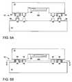
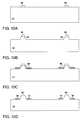
- FIGS. 1A and 1Bschematically illustrate a cross-sectional representation of a first example of the attachment structure of the present invention before and after engagement, respectively; and FIG. 1C shows a plan view of the engaged attachment structure along the section line 1 — 1 in FIG. 1 B.
- FIGS. 2A-2Dschematically illustrate a material removal process for forming a part or the entirety of the attachment structure of FIG. 1 .
- FIGS. 3A-3Dschematically illustrate an alternative material addition process for forming a part or the entirety of the attachment structure of FIG. 1 .
- FIGS. 4A-4Fschematically illustrate in cross-section view representative examples of different types of shaped pillars that can be formed according to the present invention.
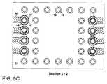
- FIGS. 5A and 5Bschematically illustrate a cross-sectional representation of a second example of the attachment structure of the present invention before and after engagement, respectively; and FIG. 5C shows a plan view of the engaged attachment structure along the section line 2 — 2 in FIG. 5 B.
- FIGS. 6A and 6Bschematically illustrate a cross-sectional representation of a third example of the attachment structure of the present invention before and after engagement, respectively; and FIG. 6C shows a plan view of the engaged attachment structure along the section line 3 — 3 in FIG. 6 B.
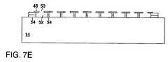
- FIGS. 7A-7Eschematically illustrate a process for fabricating a deformable layer on the supporting substrate to form a part of the attachment structure of FIGS. 6A-6C.
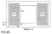
- FIGS. 8A and 8Bschematically illustrate a cross-sectional representation of a fourth example of the attachment structure of the present invention before and after engagement, respectively; and FIG. 8C shows a plan view of the engaged attachment structure along the section line 4 — 4 in FIG. 8 B.
- FIGS. 9A-9Dschematically illustrate a process for forming a plurality of recesses and an array of receptacles on a surface of a die to form a part of the attachment structure of FIGS. 8A-8C.
- FIGS. 10A-10Dschematically illustrate a process for forming a plurality of alignment pegs and an array of shaped pillars on a surface of a supporting substrate to form another part of the attachment structure of FIGS. 8A-8C.
- FIG. 11schematically illustrates in plan view a multichip module formed using the attachment structure of the present invention to attach a plurality of die to a common supporting substrate.
- FIGS. 1A-1Cthere is shown schematically a first example of the attachment structure 10 of the present invention.
- Each attachment structure 10 of the present inventionis formed in part on a first substrate 12 (also referred to herein as a die) and in part on a second substrate 14 (also referred to herein as a supporting substrate) to which the die 12 is to be attached as a part of a packaging process.
- the die 12can contain a MEM device 100 formed on or below a surface thereof; or alternately the die 12 can contain a microsensor or an integrated circuit (IC) formed thereon.
- the die 12can contain both a MEM device 100 or a microsensor together with integrated circuitry for control, signal processing or readout.
- the die 12will generally comprise a semiconductor (e.g.
- the supporting substrate 14can form a part of a conventional IC package or header, or can be attached to an IC package (not shown) prior to attachment of the die 12 to the supporting substrate 14 .
- Such attachment of the supporting substrate 14can be performed, for example, using a eutectic metal at an elevated temperature prior to attaching the die 12 to the supporting substrate 14 . In this way, exposure of the sensitive MEM device 100 to the elevated temperature can be avoided, with the attachment of the die 12 containing the MEM device 100 to the supporting substrate 14 being purely mechanical without any solder or adhesive.
- the attachment structure 10 in the example of FIGS. 1A-1Ccomprises a first plurality of shaped pillars 16 formed in or on a surface of the die 12 and extending outward therefrom, and a second plurality of shaped pillars 18 formed in or on a surface of the supporting substrate 14 and extending outward therefrom.
- the pillars 16 and 18can be formed by patterning the surfaces of the substrates 12 and 14 using a material removal process, or alternately by using a material addition process wherein one or more layers of material are deposited on the surfaces of the substrates 12 and 14 and patterned to form the pillars 16 and 18 .
- a material removal processor alternately by using a material addition process wherein one or more layers of material are deposited on the surfaces of the substrates 12 and 14 and patterned to form the pillars 16 and 18 .
- a material addition processwherein one or more layers of material are deposited on the surfaces of the substrates 12 and 14 and patterned to form the pillars 16 and 18 .
- a material conversion process in which a portion of a silicon substrate is converted to a thermal oxidecan be used to form at least a part of the attachment structure 10 .
- a thermal oxidei.e. silicon dioxide
- an ion implantation processcan be used to selectively implant portions of a silicon substrate with boron or phosphorous ions to allow patterning of the substrate by a subsequent selective etching process.
- patterned and “patterning” as used hereinmean a series of semiconductor processing steps as known to the art including steps for applying a photoresist to a surface of the substrates 12 or 14 or to a material layer thereon, pre-baking the photoresist, aligning the substrate or layer covered with photoresist with a photomask (also termed a reticle), exposing and developing the photoresist to remove the photoresist at locations where particular features (e.g. one or more pillars 16 or 18 ) are to be formed, etching downward into a portion of the substrate or into one or more material layers thereon not protected by the photoresist, and removing the remaining photoresist so that further processing can take place.
- patterned and “patterning”can also include the formation and removal of a hard mask (e.g. comprising a silicate glass) as needed.
- pillarrefers to a column or post that can be solid or hollow and of a substantially uniform width or tapered at an unsupported end thereof, but without any barbs that protrude laterally outward from the sides thereof.
- the shaped pillars 16 and 18can be meshed (i.e. engaged) when the die 12 and supporting substrate 14 are urged together. This forms a mechanical attachment due to frictional contact between the pillars 16 and 18 which are spaced in an alternating arrangement (see FIGS. 1 B and 1 C).
- the interlocking of the spaced pillars 16 and 18provides a detachable connection which securely holds the die 12 in place under normal handling and use conditions, but which allows the die 12 to later be removed from the supporting substrate if necessary.
- the force required to detach the die 12 from the supporting substrate 14will, in general, depend upon a number of factors including the tolerances used in manufacturing the pillars 16 and 18 , the surface roughness of the pillars 16 and 18 , and the number and shape of the pillars 16 and 18 .
- the pillars 16 and 18are each shown as having a circular cross-section shape in a plane parallel to the surface whereon the pillars 16 or 18 are formed.
- the pillars 16 and 18are also arranged in interlocking arrays so that each pillar 16 on the die 12 contacts a plurality of pillars 18 on the supporting substrate 14 upon engagement.
- different cross-sectional shapes for the pillars 16 and/or 18can be provided.
- one or both types of pillars 16 and 18can have an elliptical or polygonal (e.g. triangular, square, rectangular or hexagonal) cross-section shape.
- Other arbitrary shapes and sizescan be selected for the pillars 16 and 18 .
- the pillars 16 and 18be capable of being interlocked together. Furthermore, it is not necessary that the two types of shaped pillars 16 and 18 have the same cross-sectional shape. The shapes selected for the pillars 16 and 18 need only be arranged so that they mesh together upon contact and applied mounting pressure to form a mechanical attachment between the die 12 and the supporting substrate 14 .
- a sidewall of the pillars 16 or 18can be roughened; or alternately one or more ridges or notches can be formed around a sidewall of the pillars 16 or 18 (see FIGS. 4 A- 4 F). If, for example, the pillars 16 have ridges formed thereabout (see FIG. 4 A), then the mating pillars 18 can be formed with complementary notches (see FIG. 4C) which engage with the ridges to increase the strength of attachment of the die 12 to the supporting substrate 14 .
- FIGS. 2A-2Dschematically illustrate in cross-section view a series of process steps for forming the first plurality of shaped pillars 16 on the die 12 by a material removal process which removes material from the die 12 which generally comprises a semiconductor (e.g. monocrystalline silicon) to form the pillars 16 .
- the second plurality of shaped pillars 18 on the supporting substrate 14can be formed using either the material removal process or a material addition process which will be described hereinafter with reference to FIGS. 3A-3D.
- the pillars 16 and 18can be formed either by the material removal process or by the material addition process.
- a MEM device 100is fabricated in a cavity 20 etched into the die 12 using a series of conventional micromachining steps as known to the art including successive depositions and patterning of a plurality of layers of polycrystalline silicon 110 (also termed polysilicon) and a sacrificial material 120 such as silicon dioxide or a silicate glass (e.g. deposited from the decomposition of tetraethylortho silicate, also termed TEOS, and densified by heating to a high temperature).
- TEOStetraethylortho silicate
- an accelerometer structurecomprising a cantilevered beam suspended above a capacitive sense electrode) of the MEM device 100 being formed.
- the structure of the MEM device 100has been built up, one or more additional layers of the sacrificial material 120 can be deposited to fill in the cavity 20 , thereby encapsulating the MEM device 100 .
- Any of the sacrificial material extending outward above the cavity or over the surface of the die 12can be removed by chemical-mechanical polishing (CMP).
- CMPchemical-mechanical polishing
- an etch mask 22is formed over the die 12 and patterned to provide a plurality of openings 24 therethrough.
- the etch mask 22can comprise, for example, about 500 nanometers of TEOS that has been patterned by reactive ion etching using an overlying photoresist mask (not shown) which is subsequently removed to leave the etch mask 22 in place.
- an anisotropic etching step(e.g. reactive ion etching) is used to etch down into the underlying die 12 through the openings 24 in the etch mask 22 , thereby forming the plurality of shaped pillars 16 at selected locations protected by the overlying etch mask 22 .
- the reactive ion etching stepproduces sidewalls on the pillars 16 that are substantially vertical or tapered slightly inward at the top thereof (i.e. at an unsupported end of the pillars 16 ).
- the etch depthcan be, for example, 2-200 ⁇ m or more and will generally depend upon the lateral dimensions of the pillars 16 or 18 being formed which can be, for example, in the range of 5-1000 ⁇ m.
- Reactive ion etching to depths in the range of about 2-20 ⁇ mcan be accomplished using conventional reactive ion etching methods. Alternately, etching to depths greater than about 20 ⁇ m can be accomplished by using a deep reactive ion etching process which combines multiple anisotropic etching steps with steps for simultaneously depositing an isotropic polymer/inhibitor to minimize lateral etching. This deep reactive ion etching process is disclosed in U.S. Pat. No. 5,501,893 to Laermer et al, which is incorporated herein by reference.
- the etch mask 22 and sacrificial material 120 filling the cavity 20are removed. This can be done, for example, by etching away a TEOS etch mask 22 with a selective wet etchant comprising hydrofluoric acid (HF) which attacks silicon dioxide or silicate glasses while not substantially attacking silicon which is generally used for the substrates 12 and 14 and also for forming the structure of the MEM device 100 .
- a selective wet etchantcomprising hydrofluoric acid (HF) which attacks silicon dioxide or silicate glasses while not substantially attacking silicon which is generally used for the substrates 12 and 14 and also for forming the structure of the MEM device 100 .
- HFhydrofluoric acid
- FIGS. 3A-3Dschematically illustrate an alternative process which can be used to form the attachment structure 10 in the example of FIG. 1 .
- This alternative processis based on the addition of material to the die 12 or supporting substrate 14 in the form of one or more deposited and patterned layers.
- These deposited and patterned layerscan comprise one or more materials including polycrystalline silicon (i.e. polysilicon), silicon nitride, silicon dioxide, silicate glasses, polyimide, metals (e.g. aluminum or tungsten) and metal alloys.
- the material addition processwill be described with reference to formation of the shaped pillars 18 on the supporting substrate 14 , although it will be understood by those skilled in the art that this same process can be used to form the pillars 16 on the die 12 .
- a first layer of a sacrificial material 26(e.g. silicon dioxide or a silicate glass) is blanket deposited over the supporting substrate 14 and patterned to provide a plurality of openings 24 therethrough at the locations of the shaped pillars 18 to be formed.
- the first layer of the sacrificial material 26can be, for example, about 0.5-2 ⁇ mm thick.
- a layer of a pillar-forming material 28(e.g. polysilicon, silicon nitride, polyimide, or a metal or metal alloy) is blanket deposited over the patterned first layer 26 and into the openings 24 to a depth that generally exceeds the thickness of the first layer 26 .
- the depositioncan be performed by low-pressure chemical vapor deposition (LPCVD) at a temperature of about 580° C.
- LPCVDlow-pressure chemical vapor deposition
- the polyimidecan be spun on over the supporting substrate 14 and subsequently cured by heating.
- the metal or metal alloycan be deposited by evaporation, sputtering or plating.
- any excess material overlying the first layer of the sacrificial material 26can be removed by either masking off the pillar-forming material 28 deposited in the openings 24 and etching away the remaining pillar-forming material 28 , or alternately using CMP to remove any of the pillar-forming material 28 overlying the first layer of the sacrificial material 26 .
- CMPwhich is described in U.S. Pat. No. 5,804,084 to Nasby and incorporated herein by reference, produces a globally planarized surface for the supporting substrate 14 .
- the pillar-forming material 28can be annealed if necessary to remove any residual stress therein.
- the annealing stepcan be carried out at a temperature of about 1100° C. for several hours (e.g. 3 hours).
- a second layer of the sacrificial material 26is blanket deposited over the substrate 14 and patterned as described with relation to FIG. 3A.
- a second layer of the pillar-forming material 28is then deposited to fill in the openings 24 and any excess overlying the sacrificial material 26 is removed as described with relation to FIG. 3 B.
- the steps of FIGS. 3A and 3Bcan be repeated as many times as are necessary to build up the structure of the shaped pillars 18 to a predetermined length subject to limitations imposed by residual stress which cannot be removed by annealing.
- the sacrificial material 26is removed by exposure to a selective wet etchant (e.g. comprising HF) to leave the shaped pillars 18 standing on the surface of the supporting substrate 14 .
- a selective wet etchante.g. comprising HF
- the pillars 18In building up the shaped pillars 18 using the material addition process of FIGS. 3A-3D, it is not necessary that the pillars 18 have a uniform composition since different pillar-forming materials can be used to form different of the deposited layers from which the pillars 18 are built up. Additionally, it is not necessary that the pillars 18 have a uniform width along their entire length. Slight variations in the lateral dimensions of one or more of the deposited layers of the pillar-forming materials can be used to taper the pillars 18 , to roughen the sidewalls of the pillars 18 , or to form one or more internal or external ridges or notches about the sidewalls of the pillars 18 . These slight variations in the lateral dimensions of the pillars 18 can increase the force required to remove the die 12 from the supporting substrate 14 once the attachment therebetween is made.
- FIGS. 4A-4Fillustrate representative examples of different cross-sectional shapes in which the pillars 16 or 18 can be formed by varying the sizes of the openings 24 formed in successive layers of sacrificial material 26 of differing thicknesses during build-up of the structure of the pillars 16 or 18 using the material addition process of FIGS. 3A-3D.
- FIGS. 4A-4Fonly an enlarged side view of the pillar 18 is shown with the supporting substrate 14 being omitted for clarity.
- the bottom end of each pillar 18 in FIGS. 4A-4Fwill be attached to the supporting substrate 14 (not shown); and the top end of the each pillar 18 will be unsupported.
- each of the pillars 16 or 18can include one or more optional slots formed along a length thereof.
- a plurality of layers of the same or different pillar-forming materials 28are deposited in the openings 24 formed in successive layers of the sacrificial material 26 as shown in FIGS. 3A-3D.
- the pillars 18can be shaped to form one or more ridges 30 that extend laterally outward from an outer sidewall 32 of each pillar 18 .
- each pillar 18can be formed with a tapered ridged shape by anisotropically etching a plurality of openings 24 of the same or different sizes in each of the first four deposited sacrificial layers 26 as described with reference to FIG. 4 A.
- Thisforms a substantially vertical sidewall portion of the pillars 18 with one or more ridges 30 extending laterally outward therefrom.
- a tapered sidewall portion 34can then be formed at an unsupported end (i.e. the top end) of each pillar 18 by isotropically etching the opening 24 into one or more of the topmost layers of the sacrificial material 26 .
- Such isotropic etchingcan be performed, for example, with a plasma.
- a plurality of pillars 18can be formed with one or more notches 36 formed about the outer sidewall 32 thereof by using a process similar to that described with reference to FIG. 4A except with one or more openings 24 formed in the layers of the sacrificial material 26 being smaller in size than the remaining openings 24 .
- particular layers of the pillar-forming material 28can be formed with smaller lateral dimensions than the remaining layers of the pillar-forming material 28 , thereby producing a plurality of notched pillars 18 .
- a plurality of pillars 18can be formed with a roughened-sidewall shape by periodically varying the size of the openings 24 formed in a plurality of layers of sacrificial material 26 having thicknesses that are relatively thin compared to the width of the openings 24 .
- a plurality of annular-shaped openings 24can be formed in the layers of sacrificial material 26 to form hollow pillars 18 .
- the structures of the hollow pillars 18 shown in FIGS. 4E and 4Fcan be constructed.
- one or more inside ridges 38can be formed protruding outward from an inner sidewall 40 of each hollow pillar 18 towards a central axis thereof; whereas in FIG. 4F, one or more inside notches 42 can be formed extending inward from the inner sidewall 40 away from the central axis.
- FIGS. 5A-5Cshow a second example of the attachment structure 10 of the present invention.
- a plurality of hollow pillars 16 and 16 ′are formed on a die 12 which also includes a MEM device 100 formed in a cavity 20 using conventional micromachining processes as known to the art.
- the attachment structure 10further includes a plurality of solid pillars 18 and 18 ′ that are formed on a supporting substrate 14 , with the solid pillars 18 and 18 ′ mating with the hollow pillars 16 and 16 ′ to attach the die 12 to the supporting substrate 14 without the need for any solder or adhesive.
- a portion of the hollow pillars indicated as 16 ′ and a portion of the solid pillars indicated as 18 ′are made electrically conductive and thereby provide electrical interconnections between the die 12 and the supporting substrate 14 (e.g. to provide a plurality of electrical inputs or outputs to or from the MEM device 100 , or to or from electronic circuitry fabricated on the die 12 ).
- the formation of such electrical interconnectionscan in some instances completely eliminate the need for wire bonding to the die 12 .
- FIG. 5Athe die 12 and supporting substrate 14 are shown after fabrication but prior to assembly.
- FIG. 5Bshows the die 12 attached to the supporting substrate 14 using the attachment structure 10 . This can be accomplished by aligning the hollow pillars 16 and 16 ′ directly over the solid pillars 18 and 18 ′ and then urging the two substrates 12 and 14 together (e.g. using a conventional “pick and place” apparatus). Frictional contact between the hollow pillars 16 and 16 ′ and the solid pillars 18 and 18 ′ then holds the die 12 in place on the supporting substrate 14 under conditions of normal use.
- FIG. 5Cshows schematically a plan view along section line 2 — 2 of FIG. 5B to illustrate that some or all of the hollow pillars, 16 and 16 ′ can be slotted along their length as an aid in attaching the die 12 to the supporting substrate 14 .
- Providing one or more slots in the hollow pillars 16 and 16 ′increases their springiness and allows an inner diameter of the hollow pillars 16 and 16 ′ to be made more nearly equal to an outer diameter of the mating solid pillars 18 and 18 ′.
- FIG. 5Calso shows a die metallization 44 and a supporting substrate metallization 46 which are deposited and patterned to cover the pillars 16 ′ and 18 ′, respectively, and to form electrical wiring on the die 12 and on the supporting substrate 14 (e.g.
- the die metallization 44 and the substrate metallization 46can comprise aluminum or tungsten or an alloy thereof with the deposition being by evaporation, sputtering or plating to a layer thickness of, for example, 100-200 nanometers.
- such electrical wiringcan be formed by doping one or more polysilicon layers used to form the pillars 16 ′. This can be done by thermally diffusing or ion implanting a dopant species such as boron or phosphorous into the polysilicon.
- the hollow pillars 16 and 16 ′ and the solid pillars 18 and 18 ′can be formed, for example, using the material addition process as described previously with reference to FIGS. 3A-3D.
- an insulating layere.g. 100-300 nm of silicon nitride
- the pillars 16 and 18can then be built up layer by layer as described in FIGS. 3A-3D.
- the various layers of sacrificial material 26can be removed by a selective wet etchant (e.g.
- the die metallization 44(e.g. aluminum or tungsten or an alloy thereof) can then be deposited over the die 12 ′ by evaporation, sputtering or plating and can be patterned by etching (e.g. reactive ion etching) or lift-off to form a plurality of electrically-conducting hollow pillars 16 ′.
- a portion of the blanket insulating layer overlying the encapsulated MEM device 100can be removed (e.g. by reactive ion etching), or alternately a plurality of openings can be formed through the blanket insulating layer.
- the die metallization 44is generally selected to be chemically resistant to the etchant, but can be covered by a protective overlayer (e.g. silicon nitride) during the second wet etching step if this is necessary.
- the supporting substrate metallization 46can be formed similarly to the die metallization 44 except that a second wet etching step is generally not required.
- FIGS. 6A-6Cshow a third example of the attachment structure 10 of the present invention.
- a plurality of tapered pillars 16are arrayed on a lower surface of a die 12 which further includes a MEM device 100 as shown, or alternately a microsensor or integrated circuitry.
- the attachment structure 10further includes a deformable layer 48 which is formed above the supporting substrate 14 and contains a plurality of openings 50 that are superposed with the tapered pillars 16 on the die 12 , with the openings 50 having a width that is slightly smaller than the width of the pillars 16 .
- the openings 50can be shaped similarly to the pillars 16 (e.g. round as shown in FIG.
- FIG. 6 CA schematic plan view of the attachment structure 10 is shown in FIG. 6C along the section line 3 — 3 of FIG. 6 B.
- Fabrication of the tapered pillars 16 on the die 12can be carried out in a manner similar to that previously described with reference to FIGS. 3A-3D and 4 B, with the tapered pillars 16 optionally having one or more ridges or notches formed thereabout.
- Each tapered pillar 16can have a width that is generally in the range of about 5-1000 ⁇ m.
- the exact size, number and location of the pillars 16 and the corresponding openings 50 through the deformable layer 48can be selected to provide a predetermined strength of the attachment of the die 12 to the supporting substrate 14 .
- a process for fabricating the deformable layer 48 on the supporting substrate 14 by a material addition processis shown schematically in cross-section view in FIGS. 7A-7E.
- a first layer of a sacrificial material 26(e.g. silicon dioxide or a silicate glass such as TEOS) is blanket deposited over the supporting substrate 14 to a thickness of generally 1-2 ⁇ m and patterned to provide a plurality of shaped openings 24 therethrough.
- the openings 24can be, for example, circular, square or rectangular with a spacing between adjacent openings 24 of, for example, about 1.5-2 times the width of the tapered pillars 16 .
- a support material 54(e.g. polysilicon) is deposited to fill in the openings 24 .
- Any of the support material 54 overlying the first layer of the sacrificial material 26can be removed by etching or CMP.
- an annealing step(e.g. 1100° C. for three hours) can be carried out if necessary to remove any residual stress in the support material 54 .
- each layer of the support material 54can alternately be deposited first and patterned to provide a plurality of openings 24 therethrough at selected locations wherein the sacrificial material 26 is to be deposited, with the openings 24 in this case being sized to be the same as the undercut cavities 52 to be formed.
- blanket deposition of a layer of the sacrificial material 26 to fill in the openings 24any excess sacrificial material 26 overlying the deposited support material 54 can be removed by masking and etching, or alternately by CMP The result is the same as shown in FIG. 7 B.
- FIG. 7Cthe deposition and patterning steps of FIGS. 7A and 7B are repeated as many times as needed to build up the support material 54 to a predetermined thickness, which can be, for example, about 2-20 ⁇ m or more.
- the deformable layer 48is blanket deposited over the sacrificial material 26 and the support material 54 .
- the deformable layer 48can comprise, for example, polysilicon, silicon nitride, polyimide or a metal (e.g. aluminum or an alloy thereof) with a layer thickness of, for example, 0.2-2 ⁇ m depending upon the width selected for the tapered pillars 16 .
- the layer 48is patterned to provide a plurality of openings 50 therethrough. This can be done, for example, by reactive ion etching.
- the sacrificial material 26is removed from the supporting substrate 14 by etching (e.g. in a solution comprising HF). This forms undercut cavities 52 which underlie the deformable layer 48 .
- the deformable layer 48can be formed by a material removal process. This can be done, for example, by etching a plurality of trenches down into a monocrystalline silicon supporting substrate 14 to a predetermined depth. The trenches can then be filled by deposited silicon dioxide or silicate glass (e.g. TEOS), or alternately by thermally oxidizing the silicon substrate material to form silicon dioxide therefrom. The formation of a thermal oxide from a portion of the silicon substrate produces about twice the amount of the thermal oxide compared to the silicon which is consumed to form the thermal oxide.
- the deformable layer 48can then be deposited over the supporting substrate 14 and the openings 50 formed therethrough to expose the underlying silicon. An isotropic etchant (e.g. xenon difluoride) can then be used to etch away the silicon underneath the deformable layer 48 and thereby form the undercut cavities 52 and leave the deformable layer 48 intact.
- a material removal processe.g. xenon difluoride
- FIGS. 8A-8Cshow a fourth example of the attachment structure 10 of the present invention.
- the fourth example of the attachment structure 10further includes an alignment structure 56 formed in part on the die 12 and in part on the supporting substrate 14 .
- the alignment structure 56which comprises a plurality of shaped pegs 60 and shaped recesses 62 as shown in FIG. 8A, is useful for easily and precisely positioning a plurality of shaped pillars 18 on the supporting substrate 14 to micron tolerances in order to mate with a plurality of receptacles 58 arrayed on the die 12 .
- An alignment structure 56can also be optionally added to each example of the present invention described heretofore.
- the shaped pegs 60preferably have a length exceeding that of the pillars 18 so that the pegs 60 initially contact the lower surface of the die 12 , with contact between the pillars 18 and the lower surface of the die 12 being prevented until a precise alignment is achieved so that each pillar 18 can mate with its corresponding receptacle 58 . Since the width of the pegs 60 is greater than that of the receptacles 58 , the die 12 can slide over the supporting substrate 14 until each peg 60 is coarsely aligned with its corresponding shaped recess 62 .
- FIG. 8Cshows a schematic plan view of the attached die 12 and supporting substrate 14 along the section line 4 — 4 in FIG. 8 B.
- the pegs 60can be untapered; and the recesses 62 can include sloping sidewalls.
- the exact number and locations of the pegs 60 and recesses 62is a matter of design choice.
- FIGS. 9A-9Dshow a material removal method for fabricating the plurality of receptacles 58 and recesses 62 in the die 12 for attachment to the supporting substrate 14 .
- a cavity 20 and two recesses 62are formed in the die 12 .
- Thiscan be done by photolithographically masking a plurality of die 12 on a substrate or wafer (not shown) and etching each cavity 20 and recess 62 using the same etching step (e.g. reactive ion etching which forms the cavity 20 and recesses 62 with substantially vertical sidewalls, or alternately an anisotropic wet etchant such as potassium hydroxide which forms the cavity 20 and recesses 62 with sloping sidewalls).
- the cavity 20 and recesses 62are formed to the same depth which is generally in the range of 2-20 ⁇ m or more.
- the recesses 62can be formed as square openings in the die 12 as shown in FIG. 8C, with lateral dimensions (e.g. 10-1000 ⁇ m) that are generally large compared to the lateral dimensions of the receptacles 58 which are to be formed on the die 12 .
- the recesses 62can be formed to a depth greater than that of the cavity 20 . This can be done, for example, by anisotropically etching down into or completely through the die 12 from the bottom surface in FIG. 8A using an anisotropic wet etchant such as potassium hydroxide (KOH), tetramethyl ammonium hydroxide (TMAH) or ethylenediamine pyrocatechol (EDP) for a ( 100 )-oriented silicon die 12 . Etching down into the die 12 using an anisotropic wet etchant as described above will produce recesses 62 which have sidewalls that are tapered inward with increasing depth at an angle of about 55° from the surface of the die 12 .
- KOHpotassium hydroxide
- TMAHtetramethyl ammonium hydroxide
- EDPethylenediamine pyrocatechol
- a deep reactive ion etching processas disclosed in U.S. Pat. No. 5,501,893 to Laermer et al, which has been previously described with reference to FIG. 2C, can be used.
- Such a deep reactive ion etching processcan be used to etch down to hundreds of microns or even completely through the die 12 .
- Etching the recesses 62 completely through the die 12can be useful for allowing visual alignment of the pegs 60 to the recesses 62 using a microscope.
- a MEM device 100is formed within the cavity 20 using a series of alternating steps for depositing and patterning polysilicon and a sacrificial material 120 (e.g. silicon dioxide or a silicate glass).
- a sacrificial material 120e.g. silicon dioxide or a silicate glass.
- the sacrificial material 120is deposited to encapsulate each polysilicon layer and to fill the cavity 20 .
- These same depositions of the sacrificial material 120can also be used to fill in each recess 62 .
- any of the sacrificial material 120 overlying the die 12can be removed as described previously using masking and etching, or alternately using CMP
- a plurality of shaped receptacles 58can be formed in the die 12 , with the receptacles 58 generally being arrayed about each recess 62 as shown in FIG. 8 C.
- Each receptacle 58can take the shape of a circular, square or polygonal cavity depending upon the shape of the mating pillars 18 to be formed on the supporting substrate 14 .
- the lateral and vertical dimensions of each receptacle 58can be, for example, in the range of 2-100 ⁇ m.
- the receptacles 58can be formed by patterning the same surface of the die 12 wherein the recesses 62 are formed.
- each receptacle 58can be formed with substantially vertical inner sidewalls.
- the receptacles 58can be built up by a material addition process as described with reference to FIGS. 3A-3D.
- one or more notches or ridgescan easily be formed about an inner sidewall of the cavity in the receptacles 58 using the process previously described with reference to FIGS. 4E and 4F.
- the MEM device 100can be released for operation by removing the sacrificial material 120 with a selective wet etchant (e.g. a solution comprising HF). This step also removes the sacrificial material 120 from each recess 62 and completes formation of the die 12 containing its portion of the attachment structure 10 .
- a selective wet etchante.g. a solution comprising HF
- FIGS. 10A-10Dillustrate a material removal method for forming a plurality of shaped pillars 18 on the supporting substrate 14 , and a plurality of shaped alignment pegs 60 that are each shaped like a truncated pyramid.
- a patterned etch mask 66can be formed on the supporting substrate 14 with openings to expose the substrate 14 at locations wherein material is to be removed.
- the substrate 14can comprise ( 100 )-oriented monocrystalline silicon.
- an anisotropic wet etchante.g. KOH, TMAH or EDP
- KOH, TMAH or EDPan anisotropic wet etchant that substantially terminates etching upon reaching ( 111 ) crystalline planes of silicon
- This etch stepcan be timed to provide a predetermined height for the truncated pyramids, with the height being smaller than the depth of the recesses 62 formed in the die 12 .
- the etch mask 66can then be removed from the supporting substrate 14 .
- a second etch mask 68can be formed over the truncated pyramids, and over the locations wherein the shaped pillars 18 are to be formed from the substrate material.
- the second etch mask 68can be a hard mask comprising, for example, 500 nm of TEOS.
- An anisotropic etching stepcan be performed (e.g. using reactive ion etching) to etch down through the supporting substrate 14 to a predetermined depth in the regions not covered by the etch mask 68 . This forms the shaped pillars 18 which have a height that is about equal to that of the receptacles 58 formed in the die 12 .
- the pillars 18can optionally be made hollow or slotted or both depending upon a predetermined pattern used for the second etch mask 68 .
- the alignment pegs 60 and/or the pillars 18can be formed by a material addition process as described previously with reference to FIGS. 3A-3D.
- the pillars 18can include one or more notches or ridges about an outer sidewall thereof, and can also be tapered (see FIGS. 4 A- 4 C).
- removal of the second etch mask 68then completes formation of the supporting substrate 14 with its alignment pegs 60 and shaped pillars 18 .
- the supporting substrate 14can be attached to a conventional IC package (i.e. a header) prior to attachment of the die 12 to the supporting substrate 14 .
- the attachment of the supporting substrate 14 to the conventional IC packagecan be performed, for example, using a eutectic metal (e.g. a solder) heated to an elevated temperature. Since the die 12 containing the MEM device 100 , the microsensor, or the integrated circuitry is not present during the. process for attaching the supporting substrate 14 to the conventional IC package, no damage to any devices formed on the die 12 can occur. Attachment of the supporting substrate 14 to the conventional IC package using an adhesive (e.g. epoxy), however, is generally to be avoided since this can still lead to degradation of the devices on the die 12 after attachment of the die 12 to the supporting substrate 14 .
- an adhesivee.g. epoxy
- the supporting substrate 14can be the conventional IC package (e.g. comprising a ceramic, resin, or polymer material) patterned by etching, molding or replication to form a plurality of shaped pillars 18 , a deformable layer 48 or an array of receptacles 58 on or above an upper surface thereof for attachment of a die 12 to the IC package without any adhesive or solder.
- the conventional IC packagee.g. comprising a ceramic, resin, or polymer material
- a multichip module 70can be formed using a plurality of attachment structures 10 as described heretofore, with each attachment structure 10 being used to secure a die 12 containing a MEM device 100 , an IC or a microsensor to a common supporting substrate 14 as shown in the plan view of FIG.
- a patterned interconnect metallization 46 on the substrate 14can be used to electrically interconnect the various die 12 to each other and to a plurality of bond pads 72 formed on the substrate 14 .
- the actual scope of the inventionis intended to be defined in the following claims when viewed in their proper perspective based on the prior art.
Landscapes
- Engineering & Computer Science (AREA)
- Microelectronics & Electronic Packaging (AREA)
- Computer Hardware Design (AREA)
- Physics & Mathematics (AREA)
- Condensed Matter Physics & Semiconductors (AREA)
- General Physics & Mathematics (AREA)
- Power Engineering (AREA)
- Acoustics & Sound (AREA)
- Micromachines (AREA)
Abstract
Description
Claims (37)
Priority Applications (1)
| Application Number | Priority Date | Filing Date | Title |
|---|---|---|---|
| US09/516,666US6392144B1 (en) | 2000-03-01 | 2000-03-01 | Micromechanical die attachment surcharge |
Applications Claiming Priority (1)
| Application Number | Priority Date | Filing Date | Title |
|---|---|---|---|
| US09/516,666US6392144B1 (en) | 2000-03-01 | 2000-03-01 | Micromechanical die attachment surcharge |
Publications (1)
| Publication Number | Publication Date |
|---|---|
| US6392144B1true US6392144B1 (en) | 2002-05-21 |
Family
ID=24056597
Family Applications (1)
| Application Number | Title | Priority Date | Filing Date |
|---|---|---|---|
| US09/516,666Expired - LifetimeUS6392144B1 (en) | 2000-03-01 | 2000-03-01 | Micromechanical die attachment surcharge |
Country Status (1)
| Country | Link |
|---|---|
| US (1) | US6392144B1 (en) |
Cited By (44)
| Publication number | Priority date | Publication date | Assignee | Title |
|---|---|---|---|---|
| US20030035276A1 (en)* | 2001-05-28 | 2003-02-20 | Harry Hedler | Self-adhering chip |
| US20030038415A1 (en)* | 2001-08-21 | 2003-02-27 | Anderson Richard S. | Sensor isolation system |
| US20030118076A1 (en)* | 2001-09-10 | 2003-06-26 | Perkinelmer Optoelectronics Gmbh | Sensor for a contact-free temperature measurement |
| US6632400B1 (en)* | 2000-06-22 | 2003-10-14 | Agilent Technologies, Inc. | Integrated microfluidic and electronic components |
| US6673697B2 (en)* | 2002-04-03 | 2004-01-06 | Intel Corporation | Packaging microelectromechanical structures |
| US20040033676A1 (en)* | 2002-04-23 | 2004-02-19 | Stmicroelectronics S.A. | Electronic components and method of fabricating the same |
| US20040032012A1 (en)* | 2002-08-14 | 2004-02-19 | Wong Daniel M. | Hermetically packaging a microelectromechanical switch and a film bulk acoustic resonator |
| US6733681B1 (en)* | 2000-03-31 | 2004-05-11 | Seagate Technology Llc | Laterally supported handle wafer for through-wafer reactive-ion etch micromachining |
| US20040141884A1 (en)* | 1999-08-19 | 2004-07-22 | Caliper Technologies Corp. | Indicator components for microfluidic systems |
| US6809412B1 (en)* | 2002-02-06 | 2004-10-26 | Teravictu Technologies | Packaging of MEMS devices using a thermoplastic |
| US20050019974A1 (en)* | 2003-07-25 | 2005-01-27 | Markus Lutz | Anchors for microelectromechanical systems having an SOI substrate, and method of fabricating same |
| US20050180925A1 (en)* | 2003-04-16 | 2005-08-18 | Dey, L.P. | Formulations and methods for treating rhinosinusitis |
| US6936491B2 (en) | 2003-06-04 | 2005-08-30 | Robert Bosch Gmbh | Method of fabricating microelectromechanical systems and devices having trench isolated contacts |
| US20050242904A1 (en)* | 2004-04-28 | 2005-11-03 | Markus Lutz | Method for adjusting the frequency of a MEMS resonator |
| US20050247477A1 (en)* | 2004-05-04 | 2005-11-10 | Manish Kothari | Modifying the electro-mechanical behavior of devices |
| US20060001123A1 (en)* | 2004-06-30 | 2006-01-05 | John Heck | Module integrating MEMS and passive components |
| US20060033594A1 (en)* | 2004-03-04 | 2006-02-16 | Markus Lutz | Temperature controlled MEMS resonator and method for controlling resonator frequency |
| US20060108652A1 (en)* | 2003-06-04 | 2006-05-25 | Aaron Partridge | Microelectromechanical systems, and methods for encapsulating and fabricating same |
| US20060115323A1 (en)* | 2004-11-04 | 2006-06-01 | Coppeta Jonathan R | Compression and cold weld sealing methods and devices |
| US20070048899A1 (en)* | 2005-08-24 | 2007-03-01 | Wei-Chung Wang | Wafer level package and method for making the same |
| US20070114643A1 (en)* | 2005-11-22 | 2007-05-24 | Honeywell International Inc. | Mems flip-chip packaging |
| US7240420B1 (en)* | 2001-06-19 | 2007-07-10 | Zyvex Labs, Llc | System and method for post-fabrication reduction of minimum feature size spacing of microcomponents |
| US20070170528A1 (en)* | 2006-01-20 | 2007-07-26 | Aaron Partridge | Wafer encapsulated microelectromechanical structure and method of manufacturing same |
| US20080164546A1 (en)* | 2007-01-10 | 2008-07-10 | Infineon Technologies Sensonor As | Design of MEMS Packaging |
| US20080212162A1 (en)* | 2006-12-26 | 2008-09-04 | Hirotoshi Ichikawa | Method for aligning die to substrate |
| EP2015449A1 (en)* | 2007-07-13 | 2009-01-14 | ETA SA Manufacture Horlogère Suisse | Packaging for piezoelectric resonator |
| US7514283B2 (en) | 2003-03-20 | 2009-04-07 | Robert Bosch Gmbh | Method of fabricating electromechanical device having a controlled atmosphere |
| US20090127704A1 (en)* | 2007-11-20 | 2009-05-21 | Fujitsu Limited | Method and System for Providing a Reliable Semiconductor Assembly |
| US7550912B2 (en) | 2004-09-27 | 2009-06-23 | Idc, Llc | Method and system for maintaining partial vacuum in display device |
| US20090159331A1 (en)* | 2006-04-13 | 2009-06-25 | Nxp B.V. | Method for manufacturing an electronic assembly; an electronic assembly, a cover and a substrate |
| US20090309203A1 (en)* | 2008-06-16 | 2009-12-17 | Honeywell International Inc. | Getter on die in an upper sense plate designed system |
| US20100206629A1 (en)* | 2009-02-13 | 2010-08-19 | Qualcomm Mems Technologies, Inc. | Display device with desiccant |
| EP1491852A4 (en)* | 2003-02-17 | 2011-08-31 | Nippon Telegraph & Telephone | Surface shape recognition sensor and method of producing the same |
| US20110272792A1 (en)* | 2010-05-04 | 2011-11-10 | Michael Gruenhagen | Die backside standoff structures for semiconductor devices |
| US20120049350A1 (en)* | 2010-08-31 | 2012-03-01 | Globalfoundries Inc. | Stress Reduction in Chip Packaging by Using a Low-Temperature Chip-Package Connection Regime |
| US20130167482A1 (en)* | 2011-09-08 | 2013-07-04 | Advanced Numicro Systems, Inc. | Vacuum sealing process of a mems package |
| US20130181303A1 (en)* | 2012-01-17 | 2013-07-18 | Rosemount Aerospace Inc. | Die attach stress isolation |
| US20130220688A1 (en)* | 2010-11-22 | 2013-08-29 | Nec Corporation | Mounting structure and mounting method |
| US20140090234A1 (en)* | 2011-05-23 | 2014-04-03 | University Of Massachusetts | Apparatus and methods for multi-scale alignment and fastening |
| CN103985649B (en)* | 2014-06-03 | 2017-01-11 | 杭州大立微电子有限公司 | Wafer level packaging method and wafers |
| US10145739B2 (en) | 2014-04-03 | 2018-12-04 | Oto Photonics Inc. | Waveguide sheet, fabrication method thereof and spectrometer using the same |
| WO2019152095A1 (en)* | 2018-02-01 | 2019-08-08 | Hrl Laboratories, Llc | Integrated circuit with metallic interlocking structure |
| US10807864B2 (en) | 2017-01-30 | 2020-10-20 | The Regents Of The University Of Colorado, A Body Corporate | Methods of achieving universal interfacing using suspended and/or freestanding structures |
| US20240085619A1 (en)* | 2020-04-01 | 2024-03-14 | Taiwan Semiconductor Manufacturing Company, Ltd. | Semiconductor structure |
Citations (24)
| Publication number | Priority date | Publication date | Assignee | Title |
|---|---|---|---|---|
| US3266113A (en)* | 1963-10-07 | 1966-08-16 | Minnesota Mining & Mfg | Interreacting articles |
| US4531733A (en)* | 1982-07-06 | 1985-07-30 | Hall Roger E | Fastener and base using said fastener |
| US4950173A (en)* | 1983-06-15 | 1990-08-21 | Hitachi, Ltd. | Service temperature connector and packaging structure of semiconductor device employing the same |
| US5119531A (en)* | 1988-02-26 | 1992-06-09 | Michel Berger | System for joining by interengagement comprising interengaging elements formed by ridges with elastically deformable lips, in particular curvilinear |
| US5312456A (en) | 1991-01-31 | 1994-05-17 | Carnegie Mellon University | Micromechanical barb and method for making the same |
| US5347086A (en) | 1992-03-24 | 1994-09-13 | Microelectronics And Computer Technology Corporation | Coaxial die and substrate bumps |
| US5396687A (en)* | 1993-11-12 | 1995-03-14 | Osterman; Eric F. | Mechanical fastener |
| US5411400A (en)* | 1992-09-28 | 1995-05-02 | Motorola, Inc. | Interconnect system for a semiconductor chip and a substrate |
| US5501893A (en) | 1992-12-05 | 1996-03-26 | Robert Bosch Gmbh | Method of anisotropically etching silicon |
| US5532519A (en) | 1994-09-14 | 1996-07-02 | International Business Machines Corporation | Cube wireability enhancement with chip-to-chip alignment and thickness control |
| US5783340A (en) | 1995-09-06 | 1998-07-21 | Sandia Corporation | Method for photolithographic definition of recessed features on a semiconductor wafer utilizing auto-focusing alignment |
| US5798283A (en) | 1995-09-06 | 1998-08-25 | Sandia Corporation | Method for integrating microelectromechanical devices with electronic circuitry |
| US5804084A (en) | 1996-10-11 | 1998-09-08 | Sandia Corporation | Use of chemical mechanical polishing in micromachining |
| US5806152A (en) | 1996-11-15 | 1998-09-15 | Massachusetts Institute Of Technology | Compliant latching fastener |
| US5814885A (en) | 1997-04-28 | 1998-09-29 | International Business Machines Corporation | Very dense integrated circuit package |
| US5813095A (en)* | 1996-12-09 | 1998-09-29 | Robertson; Thomas Wilson | Re-closable surface binding method |
| US5818748A (en) | 1995-11-21 | 1998-10-06 | International Business Machines Corporation | Chip function separation onto separate stacked chips |
| US5848503A (en) | 1994-09-29 | 1998-12-15 | Interlego Ag | Constructional building set having an electric conductor |
| US5903059A (en) | 1995-11-21 | 1999-05-11 | International Business Machines Corporation | Microconnectors |
| US5919548A (en) | 1996-10-11 | 1999-07-06 | Sandia Corporation | Chemical-mechanical polishing of recessed microelectromechanical devices |
| US5938498A (en) | 1994-03-18 | 1999-08-17 | Ideal Ideas, Inc. | Toy construction block system with interblock connectors for extended support structures |
| US5963788A (en) | 1995-09-06 | 1999-10-05 | Sandia Corporation | Method for integrating microelectromechanical devices with electronic circuitry |
| US5988511A (en) | 1995-06-29 | 1999-11-23 | Siemens Aktiengesellschaft | Stackable data carrier that can be operated on a data bus |
| US6278193B1 (en)* | 1998-12-07 | 2001-08-21 | International Business Machines Corporation | Optical sensing method to place flip chips |
- 2000
- 2000-03-01USUS09/516,666patent/US6392144B1/ennot_activeExpired - Lifetime
Patent Citations (27)
| Publication number | Priority date | Publication date | Assignee | Title |
|---|---|---|---|---|
| US3266113A (en)* | 1963-10-07 | 1966-08-16 | Minnesota Mining & Mfg | Interreacting articles |
| US4531733A (en)* | 1982-07-06 | 1985-07-30 | Hall Roger E | Fastener and base using said fastener |
| US4950173A (en)* | 1983-06-15 | 1990-08-21 | Hitachi, Ltd. | Service temperature connector and packaging structure of semiconductor device employing the same |
| US5119531A (en)* | 1988-02-26 | 1992-06-09 | Michel Berger | System for joining by interengagement comprising interengaging elements formed by ridges with elastically deformable lips, in particular curvilinear |
| US5676850A (en) | 1991-01-31 | 1997-10-14 | Carnegie Mellon University | Micromechanical barb and method for making the same |
| US5312456A (en) | 1991-01-31 | 1994-05-17 | Carnegie Mellon University | Micromechanical barb and method for making the same |
| US5347086A (en) | 1992-03-24 | 1994-09-13 | Microelectronics And Computer Technology Corporation | Coaxial die and substrate bumps |
| US5411400A (en)* | 1992-09-28 | 1995-05-02 | Motorola, Inc. | Interconnect system for a semiconductor chip and a substrate |
| US5501893A (en) | 1992-12-05 | 1996-03-26 | Robert Bosch Gmbh | Method of anisotropically etching silicon |
| US5396687A (en)* | 1993-11-12 | 1995-03-14 | Osterman; Eric F. | Mechanical fastener |
| US5938498A (en) | 1994-03-18 | 1999-08-17 | Ideal Ideas, Inc. | Toy construction block system with interblock connectors for extended support structures |
| US5712190A (en) | 1994-09-14 | 1998-01-27 | International Business Machines Corporation | Process for controlling distance between integrated circuit chips in an electronic module |
| US5567653A (en) | 1994-09-14 | 1996-10-22 | International Business Machines Corporation | Process for aligning etch masks on an integrated circuit surface using electromagnetic energy |
| US5532519A (en) | 1994-09-14 | 1996-07-02 | International Business Machines Corporation | Cube wireability enhancement with chip-to-chip alignment and thickness control |
| US5848503A (en) | 1994-09-29 | 1998-12-15 | Interlego Ag | Constructional building set having an electric conductor |
| US5988511A (en) | 1995-06-29 | 1999-11-23 | Siemens Aktiengesellschaft | Stackable data carrier that can be operated on a data bus |
| US5783340A (en) | 1995-09-06 | 1998-07-21 | Sandia Corporation | Method for photolithographic definition of recessed features on a semiconductor wafer utilizing auto-focusing alignment |
| US5798283A (en) | 1995-09-06 | 1998-08-25 | Sandia Corporation | Method for integrating microelectromechanical devices with electronic circuitry |
| US5963788A (en) | 1995-09-06 | 1999-10-05 | Sandia Corporation | Method for integrating microelectromechanical devices with electronic circuitry |
| US5903059A (en) | 1995-11-21 | 1999-05-11 | International Business Machines Corporation | Microconnectors |
| US5818748A (en) | 1995-11-21 | 1998-10-06 | International Business Machines Corporation | Chip function separation onto separate stacked chips |
| US5804084A (en) | 1996-10-11 | 1998-09-08 | Sandia Corporation | Use of chemical mechanical polishing in micromachining |
| US5919548A (en) | 1996-10-11 | 1999-07-06 | Sandia Corporation | Chemical-mechanical polishing of recessed microelectromechanical devices |
| US5806152A (en) | 1996-11-15 | 1998-09-15 | Massachusetts Institute Of Technology | Compliant latching fastener |
| US5813095A (en)* | 1996-12-09 | 1998-09-29 | Robertson; Thomas Wilson | Re-closable surface binding method |
| US5814885A (en) | 1997-04-28 | 1998-09-29 | International Business Machines Corporation | Very dense integrated circuit package |
| US6278193B1 (en)* | 1998-12-07 | 2001-08-21 | International Business Machines Corporation | Optical sensing method to place flip chips |
Non-Patent Citations (2)
| Title |
|---|
| H. Han, L.E. Weiss and M.L. Reed, "Micromechanical Velcro," IEEE Journal of Microelectromechanical Systems, vol. 1, No. 1, pp. 37-43, Mar. 1992. |
| M.L. Reed, H. Han, and L.E. Weiss, "Silicon Micro-Velcro," Advanced Materials, vol. 4, No. 1, pp. 48-51, 1992. |
Cited By (103)
| Publication number | Priority date | Publication date | Assignee | Title |
|---|---|---|---|---|
| US20040141884A1 (en)* | 1999-08-19 | 2004-07-22 | Caliper Technologies Corp. | Indicator components for microfluidic systems |
| US6733681B1 (en)* | 2000-03-31 | 2004-05-11 | Seagate Technology Llc | Laterally supported handle wafer for through-wafer reactive-ion etch micromachining |
| US6632400B1 (en)* | 2000-06-22 | 2003-10-14 | Agilent Technologies, Inc. | Integrated microfluidic and electronic components |
| US20030035276A1 (en)* | 2001-05-28 | 2003-02-20 | Harry Hedler | Self-adhering chip |
| US6756540B2 (en)* | 2001-05-28 | 2004-06-29 | Infineon Technologies Ag | Self-adhering chip |
| US7240420B1 (en)* | 2001-06-19 | 2007-07-10 | Zyvex Labs, Llc | System and method for post-fabrication reduction of minimum feature size spacing of microcomponents |
| US20030038415A1 (en)* | 2001-08-21 | 2003-02-27 | Anderson Richard S. | Sensor isolation system |
| US7679171B2 (en) | 2001-08-21 | 2010-03-16 | The Charles Stark Draper Laboratories, Inc. | Sensor isolation system |
| US6937479B2 (en)* | 2001-08-21 | 2005-08-30 | The Charles Stark Draper Laboratory, Inc. | Sensor isolation system |
| US20030118076A1 (en)* | 2001-09-10 | 2003-06-26 | Perkinelmer Optoelectronics Gmbh | Sensor for a contact-free temperature measurement |
| US6809412B1 (en)* | 2002-02-06 | 2004-10-26 | Teravictu Technologies | Packaging of MEMS devices using a thermoplastic |
| US6673697B2 (en)* | 2002-04-03 | 2004-01-06 | Intel Corporation | Packaging microelectromechanical structures |
| US7214597B2 (en)* | 2002-04-23 | 2007-05-08 | Stmicroelectronics S.A. | Electronic components and method of fabricating the same |
| US20040033676A1 (en)* | 2002-04-23 | 2004-02-19 | Stmicroelectronics S.A. | Electronic components and method of fabricating the same |
| US20040157367A1 (en)* | 2002-08-14 | 2004-08-12 | Wong Daniel M. | Hermetically packaging a microelectromechanical switch and a film bulk acoustic resonator |
| US6713314B2 (en)* | 2002-08-14 | 2004-03-30 | Intel Corporation | Hermetically packaging a microelectromechanical switch and a film bulk acoustic resonator |
| US20040032012A1 (en)* | 2002-08-14 | 2004-02-19 | Wong Daniel M. | Hermetically packaging a microelectromechanical switch and a film bulk acoustic resonator |
| US6943419B2 (en)* | 2002-08-14 | 2005-09-13 | Intel Corporation | Hermetically packaging a microelectromechanical switch and a film bulk acoustic resonator |
| EP1491852A4 (en)* | 2003-02-17 | 2011-08-31 | Nippon Telegraph & Telephone | Surface shape recognition sensor and method of producing the same |
| US8018077B2 (en) | 2003-03-20 | 2011-09-13 | Robert Bosch Gmbh | Electromechanical system having a controlled atmosphere, and method of fabricating same |
| US9771257B2 (en) | 2003-03-20 | 2017-09-26 | Robert Bosch Gmbh | Electromechanical system having a controlled atmosphere, and method of fabricating same |
| US7514283B2 (en) | 2003-03-20 | 2009-04-07 | Robert Bosch Gmbh | Method of fabricating electromechanical device having a controlled atmosphere |
| US20090309175A1 (en)* | 2003-03-20 | 2009-12-17 | Aaron Partridge | Electromechanical system having a controlled atmosphere, and method of fabricating same |
| US20050180925A1 (en)* | 2003-04-16 | 2005-08-18 | Dey, L.P. | Formulations and methods for treating rhinosinusitis |
| US20080237756A1 (en)* | 2003-06-04 | 2008-10-02 | Aaron Partridge | Microelectromechanical systems, and methods for encapsualting and fabricating same |
| US20060108652A1 (en)* | 2003-06-04 | 2006-05-25 | Aaron Partridge | Microelectromechanical systems, and methods for encapsulating and fabricating same |
| US7288824B2 (en) | 2003-06-04 | 2007-10-30 | Robert Bosch Gmbh | Microelectromechanical systems, and devices having thin film encapsulated mechanical structures |
| US7352040B2 (en) | 2003-06-04 | 2008-04-01 | Robert Bosch Gmbh | Microelectromechanical systems having trench isolated contacts, and methods for fabricating same |
| US7075160B2 (en) | 2003-06-04 | 2006-07-11 | Robert Bosch Gmbh | Microelectromechanical systems and devices having thin film encapsulated mechanical structures |
| US6936491B2 (en) | 2003-06-04 | 2005-08-30 | Robert Bosch Gmbh | Method of fabricating microelectromechanical systems and devices having trench isolated contacts |
| US8623686B2 (en) | 2003-06-04 | 2014-01-07 | Robert Bosch Gmbh | Microelectromechanical device including an encapsulation layer of which a portion is removed to expose a substantially planar surface having a portion that is disposed outside and above a chamber and including a field region on which integrated circuits are formed, and methods for fabricating same |
| US8421167B2 (en) | 2003-06-04 | 2013-04-16 | Robert Bosch Gmbh | Microelectromechanical device including an encapsulation layer of which a portion is removed to expose a substantially planar surface having a portion that is disposed outside and above a chamber and including a field region on which integrated circuits are formed, and methods for fabricating same |
| US7859067B2 (en) | 2003-06-04 | 2010-12-28 | Robert Bosch Gmbh | Microelectromechanical device including an encapsulation layer of which a portion is removed to expose a substantially planar surface having a portion that is disposed outside and above a chamber and including a field region on which integrated circuits are formed and methods for fabricating same |
| US6952041B2 (en) | 2003-07-25 | 2005-10-04 | Robert Bosch Gmbh | Anchors for microelectromechanical systems having an SOI substrate, and method of fabricating same |
| US20050253209A1 (en)* | 2003-07-25 | 2005-11-17 | Markus Lutz | Anchors for microelectromechanical systems having an SOI substrate, and method of fabricating same |
| US20050019974A1 (en)* | 2003-07-25 | 2005-01-27 | Markus Lutz | Anchors for microelectromechanical systems having an SOI substrate, and method of fabricating same |
| US7317233B2 (en) | 2003-07-25 | 2008-01-08 | Robert Bosch Gmbh | Anchors for microelectromechanical systems having an SOI substrate, and method of fabricating same |
| US7427905B2 (en) | 2004-03-04 | 2008-09-23 | Robert Bosch Gmbh | Temperature controlled MEMS resonator and method for controlling resonator frequency |
| US7268646B2 (en) | 2004-03-04 | 2007-09-11 | Robert Bosch Gmbh | Temperature controlled MEMS resonator and method for controlling resonator frequency |
| US7068125B2 (en) | 2004-03-04 | 2006-06-27 | Robert Bosch Gmbh | Temperature controlled MEMS resonator and method for controlling resonator frequency |
| US20060033594A1 (en)* | 2004-03-04 | 2006-02-16 | Markus Lutz | Temperature controlled MEMS resonator and method for controlling resonator frequency |
| US7221241B2 (en) | 2004-04-28 | 2007-05-22 | Robert Bosch Gmbh | Method for adjusting the frequency of a MEMS resonator |
| US20050242904A1 (en)* | 2004-04-28 | 2005-11-03 | Markus Lutz | Method for adjusting the frequency of a MEMS resonator |
| US7102467B2 (en) | 2004-04-28 | 2006-09-05 | Robert Bosch Gmbh | Method for adjusting the frequency of a MEMS resonator |
| US20060255881A1 (en)* | 2004-04-28 | 2006-11-16 | Markus Lutz | Method for adjusting the frequency of a MEMS resonator |
| US20050247477A1 (en)* | 2004-05-04 | 2005-11-10 | Manish Kothari | Modifying the electro-mechanical behavior of devices |
| US7060895B2 (en)* | 2004-05-04 | 2006-06-13 | Idc, Llc | Modifying the electro-mechanical behavior of devices |
| US7161094B2 (en) | 2004-05-04 | 2007-01-09 | Idc, Llc | Modifying the electro-mechanical behavior of devices |
| US7183622B2 (en) | 2004-06-30 | 2007-02-27 | Intel Corporation | Module integrating MEMS and passive components |
| US20060001123A1 (en)* | 2004-06-30 | 2006-01-05 | John Heck | Module integrating MEMS and passive components |
| US7550912B2 (en) | 2004-09-27 | 2009-06-23 | Idc, Llc | Method and system for maintaining partial vacuum in display device |
| US20060115323A1 (en)* | 2004-11-04 | 2006-06-01 | Coppeta Jonathan R | Compression and cold weld sealing methods and devices |
| US8191756B2 (en) | 2004-11-04 | 2012-06-05 | Microchips, Inc. | Hermetically sealing using a cold welded tongue and groove structure |
| WO2006052763A3 (en)* | 2004-11-04 | 2006-09-21 | Microchips Inc | Compression and cold weld sealing methods and devices |
| US9796583B2 (en) | 2004-11-04 | 2017-10-24 | Microchips Biotech, Inc. | Compression and cold weld sealing method for an electrical via connection |
| US20070048899A1 (en)* | 2005-08-24 | 2007-03-01 | Wei-Chung Wang | Wafer level package and method for making the same |
| US7491568B2 (en)* | 2005-08-24 | 2009-02-17 | Advanced Semiconductor Engineering, Inc. | Wafer level package and method for making the same |
| US20070114643A1 (en)* | 2005-11-22 | 2007-05-24 | Honeywell International Inc. | Mems flip-chip packaging |
| US20070170528A1 (en)* | 2006-01-20 | 2007-07-26 | Aaron Partridge | Wafer encapsulated microelectromechanical structure and method of manufacturing same |
| US9440845B2 (en) | 2006-01-20 | 2016-09-13 | Sitime Corporation | Encapsulated microelectromechanical structure |
| US10099917B2 (en) | 2006-01-20 | 2018-10-16 | Sitime Corporation | Encapsulated microelectromechanical structure |
| US11685650B2 (en) | 2006-01-20 | 2023-06-27 | Sitime Corporation | Microelectromechanical structure with bonded cover |
| US10450190B2 (en) | 2006-01-20 | 2019-10-22 | Sitime Corporation | Encapsulated microelectromechanical structure |
| US20070170531A1 (en)* | 2006-01-20 | 2007-07-26 | Aaron Partridge | Wafer encapsulated microelectromechanical structure and method of manufacturing same |
| US9758371B2 (en) | 2006-01-20 | 2017-09-12 | Sitime Corporation | Encapsulated microelectromechanical structure |
| US20070170440A1 (en)* | 2006-01-20 | 2007-07-26 | Aaron Partridge | Wafer encapsulated microelectromechanical structure and method of manufacturing same |
| US20070170529A1 (en)* | 2006-01-20 | 2007-07-26 | Aaron Partridge | Wafer encapsulated microelectromechanical structure and method of manufacturing same |
| US10766768B2 (en) | 2006-01-20 | 2020-09-08 | Sitime Corporation | Encapsulated microelectromechanical structure |
| US20070172976A1 (en)* | 2006-01-20 | 2007-07-26 | Aaron Partridge | Wafer encapsulated microelectromechanical structure and method of manufacturing same |
| US20070170439A1 (en)* | 2006-01-20 | 2007-07-26 | Aaron Partridge | Wafer encapsulated microelectromechanical structure and method of manufacturing same |
| US9434608B2 (en) | 2006-01-20 | 2016-09-06 | Sitime Corporation | Wafer encapsulated microelectromechanical structure |
| US8871551B2 (en) | 2006-01-20 | 2014-10-28 | Sitime Corporation | Wafer encapsulated microelectromechanical structure and method of manufacturing same |
| US7884289B2 (en)* | 2006-04-13 | 2011-02-08 | Nxp B.V. | Method for manufacturing an electronic assembly; an electronic assembly, a cover and a substrate |
| US20090159331A1 (en)* | 2006-04-13 | 2009-06-25 | Nxp B.V. | Method for manufacturing an electronic assembly; an electronic assembly, a cover and a substrate |
| US20080212162A1 (en)* | 2006-12-26 | 2008-09-04 | Hirotoshi Ichikawa | Method for aligning die to substrate |
| WO2008085498A3 (en)* | 2006-12-26 | 2008-10-02 | Olympus Corp | Method for aligning die to substrate |
| US7848002B2 (en) | 2006-12-26 | 2010-12-07 | Silicon Quest Kabushiki-Kaisha | Method for aligning die to substrate |
| US20080164546A1 (en)* | 2007-01-10 | 2008-07-10 | Infineon Technologies Sensonor As | Design of MEMS Packaging |
| EP2015449A1 (en)* | 2007-07-13 | 2009-01-14 | ETA SA Manufacture Horlogère Suisse | Packaging for piezoelectric resonator |
| US20090127704A1 (en)* | 2007-11-20 | 2009-05-21 | Fujitsu Limited | Method and System for Providing a Reliable Semiconductor Assembly |
| US8487428B2 (en)* | 2007-11-20 | 2013-07-16 | Fujitsu Limited | Method and system for providing a reliable semiconductor assembly |
| US20090309203A1 (en)* | 2008-06-16 | 2009-12-17 | Honeywell International Inc. | Getter on die in an upper sense plate designed system |
| US7800190B2 (en)* | 2008-06-16 | 2010-09-21 | Honeywell International Inc. | Getter on die in an upper sense plate designed system |
| US8410690B2 (en) | 2009-02-13 | 2013-04-02 | Qualcomm Mems Technologies, Inc. | Display device with desiccant |
| US20100206629A1 (en)* | 2009-02-13 | 2010-08-19 | Qualcomm Mems Technologies, Inc. | Display device with desiccant |
| US8314473B2 (en)* | 2010-05-04 | 2012-11-20 | Fairchild Semiconductor Corporation | Die backside standoff structures for semiconductor devices |
| US8722528B2 (en) | 2010-05-04 | 2014-05-13 | Fairchild Semiconductor Corporation | Die backside standoff structures for semiconductor devices |
| US20110272792A1 (en)* | 2010-05-04 | 2011-11-10 | Michael Gruenhagen | Die backside standoff structures for semiconductor devices |
| US20120049350A1 (en)* | 2010-08-31 | 2012-03-01 | Globalfoundries Inc. | Stress Reduction in Chip Packaging by Using a Low-Temperature Chip-Package Connection Regime |
| US8482123B2 (en)* | 2010-08-31 | 2013-07-09 | Globalfoundries Inc. | Stress reduction in chip packaging by using a low-temperature chip-package connection regime |
| US20130220688A1 (en)* | 2010-11-22 | 2013-08-29 | Nec Corporation | Mounting structure and mounting method |
| US9204551B2 (en)* | 2010-11-22 | 2015-12-01 | Lenovo Innovations Limited (Hong Kong) | Mounting structure and mounting method |
| US20140090234A1 (en)* | 2011-05-23 | 2014-04-03 | University Of Massachusetts | Apparatus and methods for multi-scale alignment and fastening |
| US20130167482A1 (en)* | 2011-09-08 | 2013-07-04 | Advanced Numicro Systems, Inc. | Vacuum sealing process of a mems package |
| EP2990377A1 (en)* | 2012-01-17 | 2016-03-02 | Rosemount Aerospace Inc. | Die attach stress isolation |
| US8803262B2 (en)* | 2012-01-17 | 2014-08-12 | Rosemount Aerospace Inc. | Die attach stress isolation |
| US20130181303A1 (en)* | 2012-01-17 | 2013-07-18 | Rosemount Aerospace Inc. | Die attach stress isolation |
| US10145739B2 (en) | 2014-04-03 | 2018-12-04 | Oto Photonics Inc. | Waveguide sheet, fabrication method thereof and spectrometer using the same |
| CN103985649B (en)* | 2014-06-03 | 2017-01-11 | 杭州大立微电子有限公司 | Wafer level packaging method and wafers |
| US10807864B2 (en) | 2017-01-30 | 2020-10-20 | The Regents Of The University Of Colorado, A Body Corporate | Methods of achieving universal interfacing using suspended and/or freestanding structures |
| WO2019152095A1 (en)* | 2018-02-01 | 2019-08-08 | Hrl Laboratories, Llc | Integrated circuit with metallic interlocking structure |
| US20240085619A1 (en)* | 2020-04-01 | 2024-03-14 | Taiwan Semiconductor Manufacturing Company, Ltd. | Semiconductor structure |
| US12210187B2 (en)* | 2020-04-01 | 2025-01-28 | Taiwan Semiconductor Manufacturing Company, Ltd. | Semiconductor structure |
Similar Documents
| Publication | Publication Date | Title |
|---|---|---|
| US6392144B1 (en) | Micromechanical die attachment surcharge | |
| JP5313903B2 (en) | Formation of through-wafer electrical interconnects and other structures using dielectric thin films | |
| US7560802B2 (en) | Electrical connections in substrates | |
| US8679887B2 (en) | Method for manufacturing a micro-electro-mechanical device, in particular an optical microswitch, and micro-electro-mechanical device thus obtained | |
| US9923133B2 (en) | Structures and methods for testing printable integrated circuits | |
| US8258011B2 (en) | Method for producing a set of chips mechanically interconnected by means of a flexible connection | |
| US6448109B1 (en) | Wafer level method of capping multiple MEMS elements | |
| US5882532A (en) | Fabrication of single-crystal silicon structures using sacrificial-layer wafer bonding | |
| US7655538B2 (en) | MEMS device and interposer and method for integrating MEMS device and interposer | |
| US5591678A (en) | Process of manufacturing a microelectric device using a removable support substrate and etch-stop | |
| US6998533B2 (en) | Electronic device and method of manufacturing same | |
| EP1643819A2 (en) | Method of manufacturing a substrate with through electrodes | |
| US20130012024A1 (en) | Structure for microelectronics and microsystem and manufacturing process | |
| JP2009507658A (en) | MEMS device and manufacturing method | |
| US6358769B1 (en) | Process for manufacturing mechanical, electromechanical and opto-electromechanical microstructures having suspended regions subject to mechanical stresses during assembly | |
| EP1199744B1 (en) | Microcap wafer-level package | |
| JP7705209B2 (en) | Transferable pillar structure for fan-out package or interconnect bridge | |
| JP4671699B2 (en) | Manufacturing method of semiconductor capacitive acceleration sensor | |
| JP5236712B2 (en) | Manufacturing method of semiconductor capacitive acceleration sensor | |
| WO2002091439A1 (en) | Fabrication of a microelectromechanical system (mems) device | |
| CN101101370A (en) | Hinge concealed micro electromechanical device | |
| HK1137565B (en) | Formation of through-wafer electrical interconnections using an etch stop layer |
Legal Events
| Date | Code | Title | Description |
|---|---|---|---|
| AS | Assignment | Owner name:SANDIA CORPORATION, NEW MEXICO Free format text:ASSIGNMENT OF ASSIGNORS INTEREST;ASSIGNORS:FILTER, WILLIAM F.;HOHIMER, JOHN P.;REEL/FRAME:010717/0270 Effective date:20000301 | |
| AS | Assignment | Owner name:U.S. DEPARTMENT OF ENERGY, DISTRICT OF COLUMBIA Free format text:CONFIRMATORY LICENSE;ASSIGNOR:SANDIA CORPORATION;REEL/FRAME:012803/0467 Effective date:20000316 | |
| STCF | Information on status: patent grant | Free format text:PATENTED CASE | |
| CC | Certificate of correction | ||
| AS | Assignment | Owner name:U.S. DEPARTMENT OF ENERGY, DISTRICT OF COLUMBIA Free format text:CONFIRMATORY LICENSE;ASSIGNOR:SANDIA CORPORATION;REEL/FRAME:015223/0494 Effective date:20021209 | |
| FPAY | Fee payment | Year of fee payment:4 | |
| SULP | Surcharge for late payment | ||
| FPAY | Fee payment | Year of fee payment:8 | |
| FPAY | Fee payment | Year of fee payment:12 | |
| AS | Assignment | Owner name:NATIONAL TECHNOLOGY & ENGINEERING SOLUTIONS OF SAN Free format text:CHANGE OF NAME;ASSIGNOR:SANDIA CORPORATION;REEL/FRAME:043883/0237 Effective date:20170501 |