US6391753B1 - Process for forming gate conductors - Google Patents
Process for forming gate conductorsDownload PDFInfo
- Publication number
- US6391753B1 US6391753B1US09/597,624US59762400AUS6391753B1US 6391753 B1US6391753 B1US 6391753B1US 59762400 AUS59762400 AUS 59762400AUS 6391753 B1US6391753 B1US 6391753B1
- Authority
- US
- United States
- Prior art keywords
- layer
- mask
- islands
- gate
- spacer
- Prior art date
- Legal status (The legal status is an assumption and is not a legal conclusion. Google has not performed a legal analysis and makes no representation as to the accuracy of the status listed.)
- Expired - Fee Related
Links
- 238000000034methodMethods0.000titleclaimsabstractdescription49
- 230000008569processEffects0.000titleclaimsabstractdescription29
- 239000004020conductorSubstances0.000titleclaimsdescription28
- 125000006850spacer groupChemical group0.000claimsabstractdescription43
- VYPSYNLAJGMNEJ-UHFFFAOYSA-NSilicium dioxideChemical compoundO=[Si]=OVYPSYNLAJGMNEJ-UHFFFAOYSA-N0.000claimsabstractdescription28
- 239000000377silicon dioxideSubstances0.000claimsabstractdescription14
- 235000012239silicon dioxideNutrition0.000claimsabstractdescription13
- 239000000758substrateSubstances0.000claimsdescription28
- 238000004519manufacturing processMethods0.000claimsdescription13
- 239000000463materialSubstances0.000claimsdescription13
- 238000005530etchingMethods0.000claimsdescription8
- 229910021420polycrystalline siliconInorganic materials0.000claimsdescription8
- 229920005591polysiliconPolymers0.000claimsdescription8
- BOTDANWDWHJENH-UHFFFAOYSA-NTetraethyl orthosilicateChemical groupCCO[Si](OCC)(OCC)OCCBOTDANWDWHJENH-UHFFFAOYSA-N0.000claimsdescription5
- 238000000151depositionMethods0.000claimsdescription5
- 239000012212insulatorSubstances0.000claimsdescription5
- 150000004767nitridesChemical group0.000claimsdescription4
- 238000000059patterningMethods0.000claimsdescription4
- 230000008021depositionEffects0.000claimsdescription3
- 239000004065semiconductorSubstances0.000description11
- 229920002120photoresistant polymerPolymers0.000description10
- 238000005229chemical vapour depositionMethods0.000description7
- 229910052581Si3N4Inorganic materials0.000description5
- 238000001312dry etchingMethods0.000description4
- 230000005669field effectEffects0.000description4
- 239000010408filmSubstances0.000description4
- 229910044991metal oxideInorganic materials0.000description4
- 150000004706metal oxidesChemical class0.000description4
- HQVNEWCFYHHQES-UHFFFAOYSA-Nsilicon nitrideChemical compoundN12[Si]34N5[Si]62N3[Si]51N64HQVNEWCFYHHQES-UHFFFAOYSA-N0.000description4
- 230000015572biosynthetic processEffects0.000description3
- 239000010409thin filmSubstances0.000description3
- XUIMIQQOPSSXEZ-UHFFFAOYSA-NSiliconChemical compound[Si]XUIMIQQOPSSXEZ-UHFFFAOYSA-N0.000description2
- 230000000295complement effectEffects0.000description2
- 239000003989dielectric materialSubstances0.000description2
- 230000005670electromagnetic radiationEffects0.000description2
- 229910052751metalInorganic materials0.000description2
- 239000002184metalSubstances0.000description2
- 230000009467reductionEffects0.000description2
- 229910052710siliconInorganic materials0.000description2
- 239000010703siliconSubstances0.000description2
- ZOKXTWBITQBERF-UHFFFAOYSA-NMolybdenumChemical compound[Mo]ZOKXTWBITQBERF-UHFFFAOYSA-N0.000description1
- NRTOMJZYCJJWKI-UHFFFAOYSA-NTitanium nitrideChemical compound[Ti]#NNRTOMJZYCJJWKI-UHFFFAOYSA-N0.000description1
- 239000006117anti-reflective coatingSubstances0.000description1
- 230000004888barrier functionEffects0.000description1
- 230000009286beneficial effectEffects0.000description1
- 239000003990capacitorSubstances0.000description1
- 230000015556catabolic processEffects0.000description1
- 239000002800charge carrierSubstances0.000description1
- 238000006731degradation reactionMethods0.000description1
- 230000000694effectsEffects0.000description1
- 238000005516engineering processMethods0.000description1
- 229910052732germaniumInorganic materials0.000description1
- GNPVGFCGXDBREM-UHFFFAOYSA-Ngermanium atomChemical compound[Ge]GNPVGFCGXDBREM-UHFFFAOYSA-N0.000description1
- 238000002955isolationMethods0.000description1
- 238000004377microelectronicMethods0.000description1
- 229910052750molybdenumInorganic materials0.000description1
- 239000011733molybdenumSubstances0.000description1
- 238000000206photolithographyMethods0.000description1
- WFKWXMTUELFFGS-UHFFFAOYSA-NtungstenChemical compound[W]WFKWXMTUELFFGS-UHFFFAOYSA-N0.000description1
- 229910052721tungstenInorganic materials0.000description1
- 239000010937tungstenSubstances0.000description1
- 238000003631wet chemical etchingMethods0.000description1
- 238000001039wet etchingMethods0.000description1
Images


Classifications
- H—ELECTRICITY
- H01—ELECTRIC ELEMENTS
- H01L—SEMICONDUCTOR DEVICES NOT COVERED BY CLASS H10
- H01L21/00—Processes or apparatus adapted for the manufacture or treatment of semiconductor or solid state devices or of parts thereof
- H01L21/02—Manufacture or treatment of semiconductor devices or of parts thereof
- H01L21/027—Making masks on semiconductor bodies for further photolithographic processing not provided for in group H01L21/18 or H01L21/34
- H01L21/033—Making masks on semiconductor bodies for further photolithographic processing not provided for in group H01L21/18 or H01L21/34 comprising inorganic layers
- H01L21/0334—Making masks on semiconductor bodies for further photolithographic processing not provided for in group H01L21/18 or H01L21/34 comprising inorganic layers characterised by their size, orientation, disposition, behaviour, shape, in horizontal or vertical plane
- H01L21/0337—Making masks on semiconductor bodies for further photolithographic processing not provided for in group H01L21/18 or H01L21/34 comprising inorganic layers characterised by their size, orientation, disposition, behaviour, shape, in horizontal or vertical plane characterised by the process involved to create the mask, e.g. lift-off masks, sidewalls, or to modify the mask, e.g. pre-treatment, post-treatment
- H—ELECTRICITY
- H01—ELECTRIC ELEMENTS
- H01L—SEMICONDUCTOR DEVICES NOT COVERED BY CLASS H10
- H01L21/00—Processes or apparatus adapted for the manufacture or treatment of semiconductor or solid state devices or of parts thereof
- H01L21/02—Manufacture or treatment of semiconductor devices or of parts thereof
- H01L21/04—Manufacture or treatment of semiconductor devices or of parts thereof the devices having potential barriers, e.g. a PN junction, depletion layer or carrier concentration layer
- H01L21/18—Manufacture or treatment of semiconductor devices or of parts thereof the devices having potential barriers, e.g. a PN junction, depletion layer or carrier concentration layer the devices having semiconductor bodies comprising elements of Group IV of the Periodic Table or AIIIBV compounds with or without impurities, e.g. doping materials
- H01L21/28—Manufacture of electrodes on semiconductor bodies using processes or apparatus not provided for in groups H01L21/20 - H01L21/268
- H01L21/28008—Making conductor-insulator-semiconductor electrodes
- H01L21/28017—Making conductor-insulator-semiconductor electrodes the insulator being formed after the semiconductor body, the semiconductor being silicon
- H01L21/28026—Making conductor-insulator-semiconductor electrodes the insulator being formed after the semiconductor body, the semiconductor being silicon characterised by the conductor
- H01L21/28123—Lithography-related aspects, e.g. sub-lithography lengths; Isolation-related aspects, e.g. to solve problems arising at the crossing with the side of the device isolation; Planarisation aspects
- H01L21/2815—Lithography-related aspects, e.g. sub-lithography lengths; Isolation-related aspects, e.g. to solve problems arising at the crossing with the side of the device isolation; Planarisation aspects part or whole of the electrode is a sidewall spacer or made by a similar technique, e.g. transformation under mask, plating
- H—ELECTRICITY
- H01—ELECTRIC ELEMENTS
- H01L—SEMICONDUCTOR DEVICES NOT COVERED BY CLASS H10
- H01L21/00—Processes or apparatus adapted for the manufacture or treatment of semiconductor or solid state devices or of parts thereof
- H01L21/02—Manufacture or treatment of semiconductor devices or of parts thereof
- H01L21/04—Manufacture or treatment of semiconductor devices or of parts thereof the devices having potential barriers, e.g. a PN junction, depletion layer or carrier concentration layer
- H01L21/18—Manufacture or treatment of semiconductor devices or of parts thereof the devices having potential barriers, e.g. a PN junction, depletion layer or carrier concentration layer the devices having semiconductor bodies comprising elements of Group IV of the Periodic Table or AIIIBV compounds with or without impurities, e.g. doping materials
- H01L21/30—Treatment of semiconductor bodies using processes or apparatus not provided for in groups H01L21/20 - H01L21/26
- H01L21/31—Treatment of semiconductor bodies using processes or apparatus not provided for in groups H01L21/20 - H01L21/26 to form insulating layers thereon, e.g. for masking or by using photolithographic techniques; After treatment of these layers; Selection of materials for these layers
- H01L21/3205—Deposition of non-insulating-, e.g. conductive- or resistive-, layers on insulating layers; After-treatment of these layers
- H01L21/321—After treatment
- H01L21/3213—Physical or chemical etching of the layers, e.g. to produce a patterned layer from a pre-deposited extensive layer
- H01L21/32139—Physical or chemical etching of the layers, e.g. to produce a patterned layer from a pre-deposited extensive layer using masks
- H—ELECTRICITY
- H10—SEMICONDUCTOR DEVICES; ELECTRIC SOLID-STATE DEVICES NOT OTHERWISE PROVIDED FOR
- H10D—INORGANIC ELECTRIC SEMICONDUCTOR DEVICES
- H10D84/00—Integrated devices formed in or on semiconductor substrates that comprise only semiconducting layers, e.g. on Si wafers or on GaAs-on-Si wafers
- H10D84/01—Manufacture or treatment
- H10D84/0123—Integrating together multiple components covered by H10D12/00 or H10D30/00, e.g. integrating multiple IGBTs
- H10D84/0126—Integrating together multiple components covered by H10D12/00 or H10D30/00, e.g. integrating multiple IGBTs the components including insulated gates, e.g. IGFETs
- H10D84/0135—Manufacturing their gate conductors
- H—ELECTRICITY
- H10—SEMICONDUCTOR DEVICES; ELECTRIC SOLID-STATE DEVICES NOT OTHERWISE PROVIDED FOR
- H10D—INORGANIC ELECTRIC SEMICONDUCTOR DEVICES
- H10D84/00—Integrated devices formed in or on semiconductor substrates that comprise only semiconducting layers, e.g. on Si wafers or on GaAs-on-Si wafers
- H10D84/01—Manufacture or treatment
- H10D84/0123—Integrating together multiple components covered by H10D12/00 or H10D30/00, e.g. integrating multiple IGBTs
- H10D84/0126—Integrating together multiple components covered by H10D12/00 or H10D30/00, e.g. integrating multiple IGBTs the components including insulated gates, e.g. IGFETs
- H10D84/0165—Integrating together multiple components covered by H10D12/00 or H10D30/00, e.g. integrating multiple IGBTs the components including insulated gates, e.g. IGFETs the components including complementary IGFETs, e.g. CMOS devices
- H10D84/0172—Manufacturing their gate conductors
- H—ELECTRICITY
- H10—SEMICONDUCTOR DEVICES; ELECTRIC SOLID-STATE DEVICES NOT OTHERWISE PROVIDED FOR
- H10D—INORGANIC ELECTRIC SEMICONDUCTOR DEVICES
- H10D84/00—Integrated devices formed in or on semiconductor substrates that comprise only semiconducting layers, e.g. on Si wafers or on GaAs-on-Si wafers
- H10D84/01—Manufacture or treatment
- H10D84/02—Manufacture or treatment characterised by using material-based technologies
- H10D84/03—Manufacture or treatment characterised by using material-based technologies using Group IV technology, e.g. silicon technology or silicon-carbide [SiC] technology
- H10D84/038—Manufacture or treatment characterised by using material-based technologies using Group IV technology, e.g. silicon technology or silicon-carbide [SiC] technology using silicon technology, e.g. SiGe
- H—ELECTRICITY
- H10—SEMICONDUCTOR DEVICES; ELECTRIC SOLID-STATE DEVICES NOT OTHERWISE PROVIDED FOR
- H10D—INORGANIC ELECTRIC SEMICONDUCTOR DEVICES
- H10D86/00—Integrated devices formed in or on insulating or conducting substrates, e.g. formed in silicon-on-insulator [SOI] substrates or on stainless steel or glass substrates
- H10D86/01—Manufacture or treatment
- H—ELECTRICITY
- H01—ELECTRIC ELEMENTS
- H01L—SEMICONDUCTOR DEVICES NOT COVERED BY CLASS H10
- H01L21/00—Processes or apparatus adapted for the manufacture or treatment of semiconductor or solid state devices or of parts thereof
- H01L21/70—Manufacture or treatment of devices consisting of a plurality of solid state components formed in or on a common substrate or of parts thereof; Manufacture of integrated circuit devices or of parts thereof
- H01L21/71—Manufacture of specific parts of devices defined in group H01L21/70
- H01L21/768—Applying interconnections to be used for carrying current between separate components within a device comprising conductors and dielectrics
- H01L21/76838—Applying interconnections to be used for carrying current between separate components within a device comprising conductors and dielectrics characterised by the formation and the after-treatment of the conductors
Definitions
- the present applicationis related to U.S. Ser. No. 09/597,598, entitled, “A Process for Forming Multiple Active Lines and Gate-All-Around MOSFETs”, filed by Yu on an even date herewith.
- the present applicationis related to U.S. Ser. No. 09/596,993, entitled, “A Hard Mask for Integrated Circuit Fabrication”, filed by Yu on an even date herewith. Both applications are assigned to the assignee in the present application.
- the present inventionrelates to integrated circuits and methods of manufacturing integrated circuits. More particularly, the present invention relates to a method of manufacturing integrated circuits having transistors with small and/or densely packed gate conductors.
- CMOScomplementary metal oxide semiconductor
- ULSIultra-large scale integrated
- MOSFETsmetal oxide semiconductor field effect transistors
- SOIsilicon-on-insulator
- transistorssuch as, MOSFETs
- MOSFETsMOSFETs
- the substrateis doped to form source and drain regions, and a conductive layer is provided between the source and drain regions.
- the conductive layeroperates as a gate for the transistor; the gate controls current in a channel between the source and the drain regions.
- the body thickness of the transistoror thickness of depletion layer below the inversion channel must be scaled down to achieve superior short-channel performance.
- Conventional SOI-type devicesinclude an insulative substrate attached to a thin-film semiconductor substrate that contains transistors similar to the MOSFETs described with respect to bulk semiconductor-type devices.
- the insulative substrategenerally includes a buried insulative layer above a lower semiconductor base layer.
- the transistors on the insulative substratehave superior performance characteristics due to the thin-film nature of the semiconductor substrate and the insulative properties of the buried insulative layer.
- FDfully depleted
- the body thicknessis so small that the depletion region has a limited vertical extension, thereby eliminating link effect and lowering hot carrier degradation.
- the superior performance of SOI devicesis manifested in superior short-channel performance (i.e., resistance to process variation in small size transistor), near-ideal subthreshold voltage swing (i.e., good for low off-state current leakage), and high saturation current.
- Ultra-large-scale integrated (ULSI) circuitsgenerally include a multitude of transistors, such as, more than one million transistors and even several million transistors that cooperate to perform various functions for an electronic component.
- the transistorsare generally complementary metal oxide semiconductor field effect transistors (CMOSFETs) which include a gate conductor disposed between a source region and a drain region.
- CMOSFETscomplementary metal oxide semiconductor field effect transistors
- the gate conductoris provided over a thin gate oxide material.
- the gate conductorcan be a metal, a polysilicon, or polysilicon/germanium (Si x Ge (1 ⁇ x) ) material that controls charge carriers in a channel region between the drain and the source to turn the transistor on and off.
- the transistorscan be N-channel MOSFETs or P-channel MOSFETs.
- lithographic toolsare utilized to form transistors and other structures on the integrated circuit.
- lithographic toolscan be utilized to define gate conductors, conductive lines, vias, doped regions, and other structures associated with an integrated circuit.
- Most conventional lithographic fabrication processeshave only been able to define structures or regions having a dimension of 100 nm or greater.
- a photoresist maskis coated over a substrate or a layer above the substrate.
- the photoresist maskis lithographically patterned by providing electromagnetic radiation, such as, ultraviolet light, through an overlay mask.
- the portions of the photoresist mask exposed to the electromagnetic radiationreact (e.g. are cured).
- the uncured portions of the photoresist maskare removed, thereby transposing and the pattern associated with the overlay to the photoresist mask.
- the patterned photoresist maskis utilized to etch other mask layers or structures.
- the etched mask layer and structurescan be used to define doping regions, other structures, vias, lines, etc.
- lithographic techniquesare unable to precisely and accurately define the feature.
- reduction of the width of the gate conductor (the gate length) associated with a transistorhas significant beneficial effects. Future designs of transistors may require that the gate conductor have a width of less than 50 nanometers.
- An exemplary embodimentrelates to a method of manufacturing an integrated circuit including transistors.
- the transistorsinclude a first transistor having a gate structure disposed on a film.
- the methodincludes removing portions of a mask layer above a conductive layer above the film to form a mask feature, providing and removing portions of an oxide material above the mask feature in the conductive layer to leave a spacer on at least one sidewall of the mask feature.
- the methodalso includes removing the mask layer, and etching the conductive layer in accordance with the spacer, thereby forming the gate structure.
- Another exemplary embodimentrelates to a process of forming a gate conductor.
- the gate conductorhas a dimension less than one lithographic feature.
- the processincludes providing a conductive layer above a top surface of a substrate, providing a mask layer above the conductive layer, patterning the mask layer to have a sidewall, providing an insulative spacer on the sidewall of the mask layer, removing the mask layer, and etching the conductive layer in accordance with the insulative spacer. Etching the conductive layer in accordance with the insulative spacer forms the gate conductor.
- Yet another embodimentrelates to a method of manufacturing structures on a ultra-large scale integrated circuit.
- the gate structureshave at least one dimension less than 50 nm.
- the methodincludes steps of depositing a mask layer over a top surface of a conductive layer above a substrate, lithographically patterning the mask layer to have a plurality of islands, providing spacers on sidewalls of the islands, removing the islands, and removing portions of the conductive layer.
- the islandshave a dimension at least 50 nm wide.
- the portions of the conductive layerare removed in accordance with the spacers to form the gate structures.
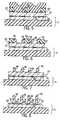
- FIG. 1is a cross-sectional view of a portion of an integrated circuit in accordance with an exemplary embodiment of the present invention, the integrated circuit including a number of gate structures provided on a semiconductor-on-insulator substrate;
- FIG. 2is a cross-sectional view of the portion of the integrated circuit illustrated in FIG. 1, showing a conductive layer formation step and a gate oxide formation step;
- FIG. 3is a cross-sectional view of the portion of the integrated circuit illustrated in FIG. 2, showing a mask deposition step and a lithographic step;
- FIG. 4is a cross-sectional view of the portion of the integrated circuit illustrated in FIG. 3, showing a mask etching step
- FIG. 5is a cross-sectional view of the portion of the integrated circuit illustrated in FIG. 4, showing an insulative layer deposition step;
- FIG. 6is a cross-sectional view of the portion of the integrated circuit illustrated in FIG. 5, showing a spacer formation step
- FIG. 7is a cross-sectional view of the portion of the integrated circuit illustrated in FIG. 6, showing a mask removal step
- FIG. 8is a cross-sectional view of the portion of the integrated circuit illustrated in FIG. 7, showing a conductive layer etching step.
- a portion 10 of an integrated circuitincludes a number of gate structures 18 .
- Gate structures 18can be part of transistors formed on a semiconductor substrate 14 , such as, a wafer.
- Semiconductor substrate 14is preferably a semiconductor-on-insulator (SOI) substrate.
- substrate 14includes a thin film semiconductor layer 15 and an insulative layer 17 .
- a semiconductive base layercan also be included.
- Layer 17is preferably a buried oxide layer, such as, silicon dioxide. Layer 17 can have a thickness of 1000-5000 ⁇ . Layer 15 is preferably a layer of silicon having a thickness of 150-200 ⁇ .
- transistors associated with structures 18can be fully formed or partially formed.
- the transistorsare part of portion 10 of the integrated circuit (IC) manufactured on a wafer (such as, a silicon bulk-type wafer or SOI wafer).
- the transistorscan include gate structure 18 , source regions, and drain regions and can be coupled to contacts, interconnects, etc.
- Gate structures 18include gate oxide structures 34 and gate conductors 36 .
- Gate oxide structures 34are preferably thermally grown silicon dioxide to thickness of 12-20 ⁇ on layer 15 of substrate 14 .
- other materialssuch as, silicon nitride (Si 3 N 4 ) high K gate dielectrics, or other insulators can be deposited by chemical vapor deposition (CVD) for structures 34 .
- Gate stack or structures 18can include spacers. The spacers can be silicon nitride, silicon dioxide (S i O 2 ) or other insulative material.
- Conductors 36are preferably deposited as undoped or doped polysilicon by chemical vapor deposition (CVD) and etched to form the particular structure for the transistors. Gate conductors 36 can traverse substrate 14 in accordance with various circuit designs. Alternatively, conductors 36 can include metal, such as, titanium nitride (TiN), Molybdenum (Mo), Tungsten (W), or other conductor. Gate conductors 36 and structures 18 preferably have a height or thickness of 1000-1500 ⁇ .
- Gate structures 18can be disposed over ultra-thin body channel regions 37 .
- Channel regions 37can have a thickness less than 200 ⁇ which reduces the susceptibility of the transistor to short channel affects such as voltage roll-off and drain induced barrier lowering.
- Channel region 37is located between source and drain regions underneath gate oxide layers 34 .
- Region 37is as thick as layer 15 associated with substrate 14 .
- gate structures 18can be provided over conventional channel regions in a bulk-type substrate.
- Gate structures 18 including conductors 36 and structures 34advantageously have a width (e.g., from left to right associated with a gate length of a transistor) of 20-50 nm.
- An advantageous processforms structures 18 without the direct use of photolithography.
- gate structures 18are spaced from 100-600 nm from each other. The reduced width associated with gate structures 18 allows multiple, densely packed transistors to be formed on substrate 14 .
- Gate structures 18can be for transistors which are N-channel or P-channel field effect transistors, such as, a metal oxide semiconductor field effect transistors (MOSFETs).
- MOSFETsmetal oxide semiconductor field effect transistors
- the transistorscan be at least partially covered by an insulative layer and is preferably part of an ultra-large scale integrated (ULSI) circuit that includes one million or more transistors.
- ULSIultra-large scale integrated
- gate structures 18can be formed which have at least one dimension (topographic) less than conventional lithographic capabilities (less than 100 nm).
- the dimension of less than one lithographic featurecan be affected by the type of lithographic equipment, the wavelength of the light from the equipment, and other lithographic factors.
- a gate oxide layer 24is deposited or thermally grown over a top surface 35 of layer 15 .
- Layer 24is associated with oxide structures 34 (FIG. 1) and is preferably thermally grown as silicon dioxide.
- a layer 37 which is associated with conductors 36 (FIG. 1)is deposited on top surface 39 of layer 24 .
- layer 37is a conductive layer, such as, a polysilicon film.
- Layer 37can have a thickness of 1000-1500 ⁇ and can be deposited by CVD.
- a layer 40is deposited on a top surface 41 of layer 37 .
- Layer 40is preferably deposited by CVD as a 100-200 ⁇ thick buffer oxide layer.
- Layer 40can be silicon dioxide deposited in a tetraethylorthosilicate (TEOS) process.
- TEOStetraethylorthosilicate
- a layer 43is provided as a cap layer, such as, a silicon nitride cap layer.
- Layer 43is deposited by CVD over a top surface 45 of layer 40 and has a thickness of 800-1500 ⁇ .
- Layer 43serves as an anti-reflective coating for superior lithographic capabilities as well as a sacrificial (dummy) mask layer.
- nitride layers or mask materialscan be utilized as layer 43 .
- a photoresist layer 49is applied above a top surface 42 of layer 37 .
- Photoresist layer 49is lithographically configured in accordance with a conventional tool to form a pattern including photoresist structures 44 .
- Various photolithographic processes and materialscan be utilized to leave structures 44 on top surface 42 of layer 43 .
- Dimensions 64 associated with structures 44are larger than the widths of conductors 36 (FIG. 1 ).
- layers 43 and 40are etched in accordance with photoresist structures 44 to leave mask features or islands 50 associated with layer 43 .
- Islands 50have a width corresponding to dimension 46 (100-500 nm)(FIG. 3) and are spaced from each other by 100 to 600 nm.
- insulative layer 46is a TEOS blanket deposited silicon dioxide layer. Insulative layer 46 is preferably thicker than islands 50 (e.g., 3000-5000 ⁇ thick).
- portions of insulating layer 46are etched to leave spacers 48 on sidewalls 54 of islands 50 .
- Spacers 48abut sidewalls 54 of islands 50 .
- layer 46utilizes a conventional anisotropic dry etch back process to leave spacers 48 .
- the width of spacers 48is preferably controlled to be less than 100 nm, preferably between 20-50 nm.
- the width of spacers 48is preferably less than the width of islands (e.g., 50 nm).
- islands 50are removed in a wet chemical etching process.
- portions of layer 40 underneath islands 50are removed.
- other removal processescan be utilized to remove islands 50 and layer 40 .
- layer 43 (islands 50 )can serve as a sacrificial (dummy) film for forming oxide hard masks (e.g., spacers 48 ).
- spacers 48act as an oxide hard mask for forming structures 18 .
- the width (from left to right) of structures 18 and oxide structures 34is preferably similar to the width of spacers 48 (e.g., less than 100 nm, preferably 20-50 nm or the spacing between islands 50 ).
- Spacers 48can have 0.04 to 0.5 the width of islands 50 .
- gate structures 18are between 100-500 nm apart (e.g., the width of islands 50 ).
- densely packed gate structures 18are formed on substrate 14 according to an oxide hard mask process which does not directly rely on conventional photolithographic etching process.
- Layers 37 and 24can be etched in a dry etching or a wet etching process. Preferably, a dry etching process selective to polysilicon is utilized to etch layer 37 . A dry etching process selective to silicon dioxide can etch layer 24 to leave structures 34 . This step can at least partially etch spacers 18 . Layers 37 and 24 form a polysilicon silicon dioxide stack for structures 18 .
- spacers 48are removed by a dry etching process selective to silicon dioxide.
- silicon nitride spacers for structure 18are formed before spacers 48 are removed to protect structures 34 from the silicon dioxide etch.
- Conventional SOI MOS fabrication processingcan be utilized to formed transistors, contacts, interconnects and interlevel dielectrics for portion.
Landscapes
- Engineering & Computer Science (AREA)
- Physics & Mathematics (AREA)
- Condensed Matter Physics & Semiconductors (AREA)
- General Physics & Mathematics (AREA)
- Manufacturing & Machinery (AREA)
- Computer Hardware Design (AREA)
- Microelectronics & Electronic Packaging (AREA)
- Power Engineering (AREA)
- Chemical & Material Sciences (AREA)
- Inorganic Chemistry (AREA)
- Thin Film Transistor (AREA)
Abstract
Description
The present application is related to U.S. Ser. No. 09/597,598, entitled, “A Process for Forming Multiple Active Lines and Gate-All-Around MOSFETs”, filed by Yu on an even date herewith. The present application is related to U.S. Ser. No. 09/596,993, entitled, “A Hard Mask for Integrated Circuit Fabrication”, filed by Yu on an even date herewith. Both applications are assigned to the assignee in the present application.
The present invention relates to integrated circuits and methods of manufacturing integrated circuits. More particularly, the present invention relates to a method of manufacturing integrated circuits having transistors with small and/or densely packed gate conductors.
Currently, deep-submicron complementary metal oxide semiconductor (CMOS) is the primary technology for ultra-large scale integrated (ULSI) circuits. Over the last two decades, reduction in the size of CMOS transistors has been a principal focus of the microelectronics industry.
Transistors, such as, metal oxide semiconductor field effect transistors (MOSFETs), are generally either bulk semiconductor-type devices or silicon-on-insulator (SOI)-type devices. Most integrated circuits are fabricated in a CMOS process on a bulk semiconductor substrate.
In bulk semiconductor-type devices, transistors, such as, MOSFETs, are built on the top surface of a bulk substrate. The substrate is doped to form source and drain regions, and a conductive layer is provided between the source and drain regions. The conductive layer operates as a gate for the transistor; the gate controls current in a channel between the source and the drain regions. As transistors become smaller, the body thickness of the transistor (or thickness of depletion layer below the inversion channel) must be scaled down to achieve superior short-channel performance.
Conventional SOI-type devices include an insulative substrate attached to a thin-film semiconductor substrate that contains transistors similar to the MOSFETs described with respect to bulk semiconductor-type devices. The insulative substrate generally includes a buried insulative layer above a lower semiconductor base layer. The transistors on the insulative substrate have superior performance characteristics due to the thin-film nature of the semiconductor substrate and the insulative properties of the buried insulative layer. In a fully depleted (FD) MOSFET, the body thickness is so small that the depletion region has a limited vertical extension, thereby eliminating link effect and lowering hot carrier degradation. The superior performance of SOI devices is manifested in superior short-channel performance (i.e., resistance to process variation in small size transistor), near-ideal subthreshold voltage swing (i.e., good for low off-state current leakage), and high saturation current.
Ultra-large-scale integrated (ULSI) circuits generally include a multitude of transistors, such as, more than one million transistors and even several million transistors that cooperate to perform various functions for an electronic component. The transistors are generally complementary metal oxide semiconductor field effect transistors (CMOSFETs) which include a gate conductor disposed between a source region and a drain region. The gate conductor is provided over a thin gate oxide material. Generally, the gate conductor can be a metal, a polysilicon, or polysilicon/germanium (SixGe(1−x)) material that controls charge carriers in a channel region between the drain and the source to turn the transistor on and off. The transistors can be N-channel MOSFETs or P-channel MOSFETs.
Generally, it is desirous to manufacture smaller transistors to increase the component density on an integrated circuit. It is also desirous to reduce the size of integrated circuit structures, such as vias, conductive lines, capacitors, resistors, isolation structures, contacts, interconnects, etc. For example, manufacturing a transistor having a reduced gate length (a reduced width of the gate conductor) can have significant benefits. Gate conductors with reduced widths can be formed more closely together, thereby increasing the transistor density on the IC. Further, gate conductors with reduced widths allow smaller transistors to be designed, thereby increasing speed and reducing power requirements for the transistors.
Heretofore, lithographic tools are utilized to form transistors and other structures on the integrated circuit. For example, lithographic tools can be utilized to define gate conductors, conductive lines, vias, doped regions, and other structures associated with an integrated circuit. Most conventional lithographic fabrication processes have only been able to define structures or regions having a dimension of 100 nm or greater.
In one type of conventional lithographic fabrication process, a photoresist mask is coated over a substrate or a layer above the substrate. The photoresist mask is lithographically patterned by providing electromagnetic radiation, such as, ultraviolet light, through an overlay mask. The portions of the photoresist mask exposed to the electromagnetic radiation react (e.g. are cured). The uncured portions of the photoresist mask are removed, thereby transposing and the pattern associated with the overlay to the photoresist mask. The patterned photoresist mask is utilized to etch other mask layers or structures. The etched mask layer and structures, in turn, can be used to define doping regions, other structures, vias, lines, etc.
As the dimensions of structures or features on the integrated circuit reach levels below 100 nm or 50 nm, lithographic techniques are unable to precisely and accurately define the feature. For example, as described above, reduction of the width of the gate conductor (the gate length) associated with a transistor has significant beneficial effects. Future designs of transistors may require that the gate conductor have a width of less than 50 nanometers.
Thus, there is a need for an integrated circuit or electronic device that includes smaller, more densely disposed gate conductors. Further still, there is a need for a ULSI circuit which does not utilize conventional lithographic techniques to define gate conductors. Even further still, there is a need for a non-lithographic approach for defining gates having at least one topographic dimension less than 100 nanometers and less than 50 nanometers (e.g., 20-50 nm). Yet further still, there is a need for an SOI integrated circuit with transistors having gate lengths of about 20 to 50 nm.
An exemplary embodiment relates to a method of manufacturing an integrated circuit including transistors. The transistors include a first transistor having a gate structure disposed on a film. The method includes removing portions of a mask layer above a conductive layer above the film to form a mask feature, providing and removing portions of an oxide material above the mask feature in the conductive layer to leave a spacer on at least one sidewall of the mask feature. The method also includes removing the mask layer, and etching the conductive layer in accordance with the spacer, thereby forming the gate structure.
Another exemplary embodiment relates to a process of forming a gate conductor. The gate conductor has a dimension less than one lithographic feature. The process includes providing a conductive layer above a top surface of a substrate, providing a mask layer above the conductive layer, patterning the mask layer to have a sidewall, providing an insulative spacer on the sidewall of the mask layer, removing the mask layer, and etching the conductive layer in accordance with the insulative spacer. Etching the conductive layer in accordance with the insulative spacer forms the gate conductor.
Yet another embodiment relates to a method of manufacturing structures on a ultra-large scale integrated circuit. The gate structures have at least one dimension less than 50 nm. The method includes steps of depositing a mask layer over a top surface of a conductive layer above a substrate, lithographically patterning the mask layer to have a plurality of islands, providing spacers on sidewalls of the islands, removing the islands, and removing portions of the conductive layer. The islands have a dimension at least 50 nm wide. The portions of the conductive layer are removed in accordance with the spacers to form the gate structures.
Exemplary embodiments will hereafter be described with reference to the accompanying drawings, wherein like numerals denote like elements, and:
FIG. 1 is a cross-sectional view of a portion of an integrated circuit in accordance with an exemplary embodiment of the present invention, the integrated circuit including a number of gate structures provided on a semiconductor-on-insulator substrate;
FIG. 2 is a cross-sectional view of the portion of the integrated circuit illustrated in FIG. 1, showing a conductive layer formation step and a gate oxide formation step;
FIG. 3 is a cross-sectional view of the portion of the integrated circuit illustrated in FIG. 2, showing a mask deposition step and a lithographic step;
FIG. 4 is a cross-sectional view of the portion of the integrated circuit illustrated in FIG. 3, showing a mask etching step;
FIG. 5 is a cross-sectional view of the portion of the integrated circuit illustrated in FIG. 4, showing an insulative layer deposition step;
FIG. 6 is a cross-sectional view of the portion of the integrated circuit illustrated in FIG. 5, showing a spacer formation step;
FIG. 7 is a cross-sectional view of the portion of the integrated circuit illustrated in FIG. 6, showing a mask removal step; and
FIG. 8 is a cross-sectional view of the portion of the integrated circuit illustrated in FIG. 7, showing a conductive layer etching step.
With reference to FIG. 1, aportion 10 of an integrated circuit (IC) includes a number ofgate structures 18.Gate structures 18 can be part of transistors formed on asemiconductor substrate 14, such as, a wafer.Semiconductor substrate 14 is preferably a semiconductor-on-insulator (SOI) substrate. Preferably,substrate 14 includes a thinfilm semiconductor layer 15 and aninsulative layer 17. A semiconductive base layer can also be included.
As shown in FIG. 1, transistors associated withstructures 18 can be fully formed or partially formed. The transistors are part ofportion 10 of the integrated circuit (IC) manufactured on a wafer (such as, a silicon bulk-type wafer or SOI wafer). The transistors can includegate structure 18, source regions, and drain regions and can be coupled to contacts, interconnects, etc.
With reference to FIGS. 1-8, the fabrication ofgate structures 18 is described below as follows. As discussed above with reference to FIG. 1,gate structures 18 can be formed which have at least one dimension (topographic) less than conventional lithographic capabilities (less than 100 nm). The dimension of less than one lithographic feature can be affected by the type of lithographic equipment, the wavelength of the light from the equipment, and other lithographic factors.
In FIG. 2, agate oxide layer 24 is deposited or thermally grown over atop surface 35 oflayer 15.Layer 24 is associated with oxide structures34 (FIG. 1) and is preferably thermally grown as silicon dioxide. Alayer 37 which is associated with conductors36 (FIG. 1) is deposited ontop surface 39 oflayer 24. Preferably,layer 37 is a conductive layer, such as, a polysilicon film.Layer 37 can have a thickness of 1000-1500 Å and can be deposited by CVD.
In FIG. 3, afterlayer 37 is deposited, alayer 40 is deposited on atop surface 41 oflayer 37.Layer 40 is preferably deposited by CVD as a 100-200 Å thick buffer oxide layer.Layer 40 can be silicon dioxide deposited in a tetraethylorthosilicate (TEOS) process.
Afterlayer 40 is provided, alayer 43 is provided as a cap layer, such as, a silicon nitride cap layer.Layer 43 is deposited by CVD over atop surface 45 oflayer 40 and has a thickness of 800-1500 Å.Layer 43 serves as an anti-reflective coating for superior lithographic capabilities as well as a sacrificial (dummy) mask layer. Alternatively, other nitride layers or mask materials can be utilized aslayer 43.
In FIG. 3, aphotoresist layer 49 is applied above atop surface 42 oflayer 37.Photoresist layer 49 is lithographically configured in accordance with a conventional tool to form a pattern includingphotoresist structures 44. Various photolithographic processes and materials can be utilized to leavestructures 44 ontop surface 42 oflayer 43.Dimensions 64 associated withstructures 44 are larger than the widths of conductors36 (FIG.1). In FIG. 4, afterstructures 44 are formed, layers43 and40 are etched in accordance withphotoresist structures 44 to leave mask features orislands 50 associated withlayer 43.Islands 50 have a width corresponding to dimension46 (100-500 nm)(FIG. 3) and are spaced from each other by 100 to 600 nm.
In FIG. 5,islands 50 andlayer 37 are covered by anon-conformal insulative layer 46. Preferably,insulative layer 46 is a TEOS blanket deposited silicon dioxide layer.Insulative layer 46 is preferably thicker than islands50 (e.g., 3000-5000 Å thick).
In FIG. 6, portions of insulatinglayer 46 are etched to leavespacers 48 onsidewalls 54 ofislands 50.Spacers 48 abut sidewalls54 ofislands 50. Preferably,layer 46 utilizes a conventional anisotropic dry etch back process to leavespacers 48. The width ofspacers 48 is preferably controlled to be less than 100 nm, preferably between 20-50 nm. The width ofspacers 48 is preferably less than the width of islands (e.g., 50 nm).
In FIG. 7, after spacers48 are formed,islands 50 are removed in a wet chemical etching process. In addition, portions oflayer 40 underneathislands 50 are removed. Alternatively, other removal processes can be utilized to removeislands 50 andlayer 40. Thus, layer43 (islands50) can serve as a sacrificial (dummy) film for forming oxide hard masks (e.g., spacers48).
In FIG. 8, layers37 and35 are etched in accordance withspacers 48 to leavegate structures 18. Thus, spacers48 act as an oxide hard mask for formingstructures 18. The width (from left to right) ofstructures 18 andoxide structures 34 is preferably similar to the width of spacers48 (e.g., less than 100 nm, preferably 20-50 nm or the spacing between islands50).Spacers 48 can have 0.04 to 0.5 the width ofislands 50. Generally,gate structures 18 are between 100-500 nm apart (e.g., the width of islands50). Thus, densely packedgate structures 18 are formed onsubstrate 14 according to an oxide hard mask process which does not directly rely on conventional photolithographic etching process.
In FIG. 1,spacers 48 are removed by a dry etching process selective to silicon dioxide. In one embodiment, silicon nitride spacers forstructure 18 are formed before spacers48 are removed to protectstructures 34 from the silicon dioxide etch. Conventional SOI MOS fabrication processing can be utilized to formed transistors, contacts, interconnects and interlevel dielectrics for portion.
It is understood that while the detailed drawings, specific examples, and particular values given provide a preferred exemplary embodiment of the present invention, the preferred exemplary embodiment is for the purpose of illustration only. The method and apparatus of the invention is not limited to the precise details and conditions disclosed. For example, although SOI substrates are shown, other substrates can be utilized. Various changes may be made to the details disclosed without departing from the spirit of the invention which is defined by the following claims.
Claims (20)
1. A method of manufacturing an integrated circuit including a plurality of transistors, the plurality of transistors including a first transistor having a gate structure disposed on a film, the method comprising:
removing portions of a mask layer above a conductive layer above the film to form a mask feature, the mask feature having at least one sidewall;
providing an oxide material above the mask, the oxide material being a thick, non-conformal layer;
removing portions of the oxide material above the mask feature and the conductive layer to leave a spacer on the at least one sidewall;
removing the mask feature; and
etching the conductive layer in accordance with the spacer, thereby forming the gate structure.
2. The method ofclaim 1 , wherein the gate structure has a width between 20 nm and 50 nm.
3. The method ofclaim 2 , wherein an oxide layer is disposed between the mask layer and the conductive layer.
4. The method ofclaim 1 , wherein the mask layer is a nitride layer and the conductive layer is a polysilicon layer.
5. The method ofclaim 1 , wherein the film is part of a silicon-on-insulator substrate.
6. The method ofclaim 5 , wherein the spacer is 0.04 to 0.5 times as wide as the mask feature.
7. A process of forming a gate conductor having a dimension less than one lithographic feature, the process comprising:
providing a conductive layer above a top surface of a substrate;
providing a mask layer above the conductive layer, the mask layer having a first thickness;
patterning the mask layer to have a sidewall;
providing a non-conformal insulative material above the mask layer, the insulative material having a second thickness greater than the first thickness;
forming an insulative spacer from the insulative material on the sidewall of the mask layer;
removing the mask layer; and
etching the conductive layer in accordance with the insulative spacer as a mask to form the gate conductor.
8. The process ofclaim 7 , wherein the gate conductor includes polysilicon.
9. The process ofclaim 8 , wherein the mask layer includes nitride.
10. The process ofclaim 7 , wherein a plurality of gate structures are formed and the providing step includes forming a plurality of insulative spacers on respective sidewalls of the mask layer.
11. The process ofclaim 7 , wherein a gate oxide layer is below the conductive layer.
12. The process ofclaim 7 wherein the insulative spacer is 20-50 nm wide.
13. The process ofclaim 12 , wherein the insulative spacer is TEOS deposited silicon dioxide.
14. A method of manufacturing a plurality of gate structures on an ultra-large scale integrated circuit, the gate structures having at least one dimension less than 50 nm, the method comprising steps of:
depositing a mask layer over a top surface of a conductive layer above a substrate;
lithographically patterning the mask layer to have a plurality of islands, the islands having a minimum topographic dimension at least 50 nm wide;
providing a non-conformal spacer layer above the islands, the spacer layer at least completely filling the gaps between the islands;
forming spacers on sidewalls of the islands from the spacer layer;
removing the islands; and
removing portions of the conductive layer in accordance with the spacers, the spacers being a hard mask for the removing portions step.
15. The method ofclaim 14 , wherein the islands are spaced from each other at least 100 nm.
16. The method ofclaim 15 , wherein the islands are between 100-500 nm wide.
17. The method ofclaim 16 , wherein the spacers are 20-50 nm wide.
18. The method ofclaim 14 , forming the spacers step is a deposition and etch back step.
19. The method ofclaim 18 , wherein the spacers include TEOS deposited silicon dioxide.
20. The method ofclaim 14 , wherein the mask layer includes nitride.
Priority Applications (1)
| Application Number | Priority Date | Filing Date | Title |
|---|---|---|---|
| US09/597,624US6391753B1 (en) | 2000-06-20 | 2000-06-20 | Process for forming gate conductors |
Applications Claiming Priority (1)
| Application Number | Priority Date | Filing Date | Title |
|---|---|---|---|
| US09/597,624US6391753B1 (en) | 2000-06-20 | 2000-06-20 | Process for forming gate conductors |
Publications (1)
| Publication Number | Publication Date |
|---|---|
| US6391753B1true US6391753B1 (en) | 2002-05-21 |
Family
ID=24392271
Family Applications (1)
| Application Number | Title | Priority Date | Filing Date |
|---|---|---|---|
| US09/597,624Expired - Fee RelatedUS6391753B1 (en) | 2000-06-20 | 2000-06-20 | Process for forming gate conductors |
Country Status (1)
| Country | Link |
|---|---|
| US (1) | US6391753B1 (en) |
Cited By (149)
| Publication number | Priority date | Publication date | Assignee | Title |
|---|---|---|---|---|
| US6451656B1 (en)* | 2001-02-28 | 2002-09-17 | Advanced Micro Devices, Inc. | CMOS inverter configured from double gate MOSFET and method of fabricating same |
| US6664180B1 (en) | 2001-04-02 | 2003-12-16 | Advanced Micro Devices, Inc. | Method of forming smaller trench line width using a spacer hard mask |
| US6664173B2 (en)* | 2002-01-09 | 2003-12-16 | Intel Corporation | Hardmask gate patterning technique for all transistors using spacer gate approach for critical dimension control |
| US6872647B1 (en)* | 2003-05-06 | 2005-03-29 | Advanced Micro Devices, Inc. | Method for forming multiple fins in a semiconductor device |
| US20080206934A1 (en)* | 2007-02-23 | 2008-08-28 | Jones Robert E | Forming semiconductor fins using a sacrificial fin |
| CN100524610C (en)* | 2005-06-17 | 2009-08-05 | 旺宏电子股份有限公司 | Method for fabricating narrow structures on an integrated circuit |
| US20090224357A1 (en)* | 2008-03-06 | 2009-09-10 | Micron Technology, Inc. | Devices with cavity-defined gates and methods of making the same |
| US20110021010A1 (en)* | 2009-07-27 | 2011-01-27 | International Business Machines Corporation | Method for double pattern density |
| US20110127582A1 (en)* | 2009-12-01 | 2011-06-02 | International Business Machines Corporation | Multiplying pattern density by single sidewall imaging transfer |
| US20110143503A1 (en)* | 2006-11-30 | 2011-06-16 | Kabushiki Kaisha Toshiba | Semiconductor storage element and manufacturing method thereof |
| US20150214337A1 (en)* | 2014-01-27 | 2015-07-30 | Applied Materials, Inc. | Method of fin patterning |
| US9117855B2 (en) | 2013-12-04 | 2015-08-25 | Applied Materials, Inc. | Polarity control for remote plasma |
| US9132436B2 (en) | 2012-09-21 | 2015-09-15 | Applied Materials, Inc. | Chemical control features in wafer process equipment |
| US9136273B1 (en) | 2014-03-21 | 2015-09-15 | Applied Materials, Inc. | Flash gate air gap |
| US9153442B2 (en) | 2013-03-15 | 2015-10-06 | Applied Materials, Inc. | Processing systems and methods for halide scavenging |
| US9159606B1 (en) | 2014-07-31 | 2015-10-13 | Applied Materials, Inc. | Metal air gap |
| US9165786B1 (en) | 2014-08-05 | 2015-10-20 | Applied Materials, Inc. | Integrated oxide and nitride recess for better channel contact in 3D architectures |
| US9190293B2 (en) | 2013-12-18 | 2015-11-17 | Applied Materials, Inc. | Even tungsten etch for high aspect ratio trenches |
| US9209012B2 (en) | 2013-09-16 | 2015-12-08 | Applied Materials, Inc. | Selective etch of silicon nitride |
| US9236266B2 (en) | 2011-08-01 | 2016-01-12 | Applied Materials, Inc. | Dry-etch for silicon-and-carbon-containing films |
| US9236265B2 (en) | 2013-11-04 | 2016-01-12 | Applied Materials, Inc. | Silicon germanium processing |
| US9245762B2 (en) | 2013-12-02 | 2016-01-26 | Applied Materials, Inc. | Procedure for etch rate consistency |
| US9263278B2 (en) | 2013-12-17 | 2016-02-16 | Applied Materials, Inc. | Dopant etch selectivity control |
| US9269590B2 (en) | 2014-04-07 | 2016-02-23 | Applied Materials, Inc. | Spacer formation |
| US9287095B2 (en) | 2013-12-17 | 2016-03-15 | Applied Materials, Inc. | Semiconductor system assemblies and methods of operation |
| US9287134B2 (en) | 2014-01-17 | 2016-03-15 | Applied Materials, Inc. | Titanium oxide etch |
| US9299538B2 (en) | 2014-03-20 | 2016-03-29 | Applied Materials, Inc. | Radial waveguide systems and methods for post-match control of microwaves |
| US9299583B1 (en) | 2014-12-05 | 2016-03-29 | Applied Materials, Inc. | Aluminum oxide selective etch |
| US9299537B2 (en) | 2014-03-20 | 2016-03-29 | Applied Materials, Inc. | Radial waveguide systems and methods for post-match control of microwaves |
| US9299582B2 (en) | 2013-11-12 | 2016-03-29 | Applied Materials, Inc. | Selective etch for metal-containing materials |
| US9299575B2 (en) | 2014-03-17 | 2016-03-29 | Applied Materials, Inc. | Gas-phase tungsten etch |
| US9309598B2 (en) | 2014-05-28 | 2016-04-12 | Applied Materials, Inc. | Oxide and metal removal |
| US9324576B2 (en) | 2010-05-27 | 2016-04-26 | Applied Materials, Inc. | Selective etch for silicon films |
| US9343272B1 (en) | 2015-01-08 | 2016-05-17 | Applied Materials, Inc. | Self-aligned process |
| US9349605B1 (en) | 2015-08-07 | 2016-05-24 | Applied Materials, Inc. | Oxide etch selectivity systems and methods |
| US9355863B2 (en) | 2012-12-18 | 2016-05-31 | Applied Materials, Inc. | Non-local plasma oxide etch |
| US9355856B2 (en) | 2014-09-12 | 2016-05-31 | Applied Materials, Inc. | V trench dry etch |
| US9355862B2 (en) | 2014-09-24 | 2016-05-31 | Applied Materials, Inc. | Fluorine-based hardmask removal |
| US9362130B2 (en) | 2013-03-01 | 2016-06-07 | Applied Materials, Inc. | Enhanced etching processes using remote plasma sources |
| US9368364B2 (en) | 2014-09-24 | 2016-06-14 | Applied Materials, Inc. | Silicon etch process with tunable selectivity to SiO2 and other materials |
| US9373522B1 (en) | 2015-01-22 | 2016-06-21 | Applied Mateials, Inc. | Titanium nitride removal |
| US9373517B2 (en) | 2012-08-02 | 2016-06-21 | Applied Materials, Inc. | Semiconductor processing with DC assisted RF power for improved control |
| US9378969B2 (en) | 2014-06-19 | 2016-06-28 | Applied Materials, Inc. | Low temperature gas-phase carbon removal |
| US9378978B2 (en) | 2014-07-31 | 2016-06-28 | Applied Materials, Inc. | Integrated oxide recess and floating gate fin trimming |
| US9385028B2 (en) | 2014-02-03 | 2016-07-05 | Applied Materials, Inc. | Air gap process |
| US9384997B2 (en) | 2012-11-20 | 2016-07-05 | Applied Materials, Inc. | Dry-etch selectivity |
| US9390937B2 (en) | 2012-09-20 | 2016-07-12 | Applied Materials, Inc. | Silicon-carbon-nitride selective etch |
| US9396989B2 (en) | 2014-01-27 | 2016-07-19 | Applied Materials, Inc. | Air gaps between copper lines |
| US9406523B2 (en) | 2014-06-19 | 2016-08-02 | Applied Materials, Inc. | Highly selective doped oxide removal method |
| US9412608B2 (en) | 2012-11-30 | 2016-08-09 | Applied Materials, Inc. | Dry-etch for selective tungsten removal |
| US9418858B2 (en) | 2011-10-07 | 2016-08-16 | Applied Materials, Inc. | Selective etch of silicon by way of metastable hydrogen termination |
| US9425058B2 (en) | 2014-07-24 | 2016-08-23 | Applied Materials, Inc. | Simplified litho-etch-litho-etch process |
| US9437451B2 (en) | 2012-09-18 | 2016-09-06 | Applied Materials, Inc. | Radical-component oxide etch |
| US9449845B2 (en) | 2012-12-21 | 2016-09-20 | Applied Materials, Inc. | Selective titanium nitride etching |
| US9449846B2 (en) | 2015-01-28 | 2016-09-20 | Applied Materials, Inc. | Vertical gate separation |
| US9478432B2 (en) | 2014-09-25 | 2016-10-25 | Applied Materials, Inc. | Silicon oxide selective removal |
| US9493879B2 (en) | 2013-07-12 | 2016-11-15 | Applied Materials, Inc. | Selective sputtering for pattern transfer |
| US9496167B2 (en) | 2014-07-31 | 2016-11-15 | Applied Materials, Inc. | Integrated bit-line airgap formation and gate stack post clean |
| US9502258B2 (en) | 2014-12-23 | 2016-11-22 | Applied Materials, Inc. | Anisotropic gap etch |
| US9499898B2 (en) | 2014-03-03 | 2016-11-22 | Applied Materials, Inc. | Layered thin film heater and method of fabrication |
| US9553102B2 (en) | 2014-08-19 | 2017-01-24 | Applied Materials, Inc. | Tungsten separation |
| US9576809B2 (en) | 2013-11-04 | 2017-02-21 | Applied Materials, Inc. | Etch suppression with germanium |
| US9607856B2 (en) | 2013-03-05 | 2017-03-28 | Applied Materials, Inc. | Selective titanium nitride removal |
| US9659753B2 (en) | 2014-08-07 | 2017-05-23 | Applied Materials, Inc. | Grooved insulator to reduce leakage current |
| US9691645B2 (en) | 2015-08-06 | 2017-06-27 | Applied Materials, Inc. | Bolted wafer chuck thermal management systems and methods for wafer processing systems |
| US9721789B1 (en) | 2016-10-04 | 2017-08-01 | Applied Materials, Inc. | Saving ion-damaged spacers |
| US9728437B2 (en) | 2015-02-03 | 2017-08-08 | Applied Materials, Inc. | High temperature chuck for plasma processing systems |
| US9741593B2 (en) | 2015-08-06 | 2017-08-22 | Applied Materials, Inc. | Thermal management systems and methods for wafer processing systems |
| US9768034B1 (en) | 2016-11-11 | 2017-09-19 | Applied Materials, Inc. | Removal methods for high aspect ratio structures |
| US9773648B2 (en) | 2013-08-30 | 2017-09-26 | Applied Materials, Inc. | Dual discharge modes operation for remote plasma |
| US9842744B2 (en) | 2011-03-14 | 2017-12-12 | Applied Materials, Inc. | Methods for etch of SiN films |
| US9847289B2 (en) | 2014-05-30 | 2017-12-19 | Applied Materials, Inc. | Protective via cap for improved interconnect performance |
| US9865484B1 (en) | 2016-06-29 | 2018-01-09 | Applied Materials, Inc. | Selective etch using material modification and RF pulsing |
| US9881805B2 (en) | 2015-03-02 | 2018-01-30 | Applied Materials, Inc. | Silicon selective removal |
| US9885117B2 (en) | 2014-03-31 | 2018-02-06 | Applied Materials, Inc. | Conditioned semiconductor system parts |
| US9887096B2 (en) | 2012-09-17 | 2018-02-06 | Applied Materials, Inc. | Differential silicon oxide etch |
| US9934942B1 (en) | 2016-10-04 | 2018-04-03 | Applied Materials, Inc. | Chamber with flow-through source |
| US9947549B1 (en) | 2016-10-10 | 2018-04-17 | Applied Materials, Inc. | Cobalt-containing material removal |
| US10026621B2 (en) | 2016-11-14 | 2018-07-17 | Applied Materials, Inc. | SiN spacer profile patterning |
| US10043684B1 (en) | 2017-02-06 | 2018-08-07 | Applied Materials, Inc. | Self-limiting atomic thermal etching systems and methods |
| US10043674B1 (en) | 2017-08-04 | 2018-08-07 | Applied Materials, Inc. | Germanium etching systems and methods |
| US10049891B1 (en) | 2017-05-31 | 2018-08-14 | Applied Materials, Inc. | Selective in situ cobalt residue removal |
| US10062585B2 (en) | 2016-10-04 | 2018-08-28 | Applied Materials, Inc. | Oxygen compatible plasma source |
| US10062587B2 (en) | 2012-07-18 | 2018-08-28 | Applied Materials, Inc. | Pedestal with multi-zone temperature control and multiple purge capabilities |
| US10062575B2 (en) | 2016-09-09 | 2018-08-28 | Applied Materials, Inc. | Poly directional etch by oxidation |
| US10062579B2 (en) | 2016-10-07 | 2018-08-28 | Applied Materials, Inc. | Selective SiN lateral recess |
| US10062578B2 (en) | 2011-03-14 | 2018-08-28 | Applied Materials, Inc. | Methods for etch of metal and metal-oxide films |
| US10128086B1 (en) | 2017-10-24 | 2018-11-13 | Applied Materials, Inc. | Silicon pretreatment for nitride removal |
| US10163696B2 (en) | 2016-11-11 | 2018-12-25 | Applied Materials, Inc. | Selective cobalt removal for bottom up gapfill |
| US10170336B1 (en) | 2017-08-04 | 2019-01-01 | Applied Materials, Inc. | Methods for anisotropic control of selective silicon removal |
| US10170282B2 (en) | 2013-03-08 | 2019-01-01 | Applied Materials, Inc. | Insulated semiconductor faceplate designs |
| US10224210B2 (en) | 2014-12-09 | 2019-03-05 | Applied Materials, Inc. | Plasma processing system with direct outlet toroidal plasma source |
| US10242908B2 (en) | 2016-11-14 | 2019-03-26 | Applied Materials, Inc. | Airgap formation with damage-free copper |
| US10256112B1 (en) | 2017-12-08 | 2019-04-09 | Applied Materials, Inc. | Selective tungsten removal |
| US10283324B1 (en) | 2017-10-24 | 2019-05-07 | Applied Materials, Inc. | Oxygen treatment for nitride etching |
| US10283321B2 (en) | 2011-01-18 | 2019-05-07 | Applied Materials, Inc. | Semiconductor processing system and methods using capacitively coupled plasma |
| US10297458B2 (en) | 2017-08-07 | 2019-05-21 | Applied Materials, Inc. | Process window widening using coated parts in plasma etch processes |
| US10319600B1 (en) | 2018-03-12 | 2019-06-11 | Applied Materials, Inc. | Thermal silicon etch |
| US10319649B2 (en) | 2017-04-11 | 2019-06-11 | Applied Materials, Inc. | Optical emission spectroscopy (OES) for remote plasma monitoring |
| US10319739B2 (en) | 2017-02-08 | 2019-06-11 | Applied Materials, Inc. | Accommodating imperfectly aligned memory holes |
| US10354889B2 (en) | 2017-07-17 | 2019-07-16 | Applied Materials, Inc. | Non-halogen etching of silicon-containing materials |
| US10403507B2 (en) | 2017-02-03 | 2019-09-03 | Applied Materials, Inc. | Shaped etch profile with oxidation |
| US10431429B2 (en) | 2017-02-03 | 2019-10-01 | Applied Materials, Inc. | Systems and methods for radial and azimuthal control of plasma uniformity |
| US10468267B2 (en) | 2017-05-31 | 2019-11-05 | Applied Materials, Inc. | Water-free etching methods |
| US10490406B2 (en) | 2018-04-10 | 2019-11-26 | Appled Materials, Inc. | Systems and methods for material breakthrough |
| US10490418B2 (en) | 2014-10-14 | 2019-11-26 | Applied Materials, Inc. | Systems and methods for internal surface conditioning assessment in plasma processing equipment |
| US10497573B2 (en) | 2018-03-13 | 2019-12-03 | Applied Materials, Inc. | Selective atomic layer etching of semiconductor materials |
| US10504754B2 (en) | 2016-05-19 | 2019-12-10 | Applied Materials, Inc. | Systems and methods for improved semiconductor etching and component protection |
| US10504700B2 (en) | 2015-08-27 | 2019-12-10 | Applied Materials, Inc. | Plasma etching systems and methods with secondary plasma injection |
| US10522371B2 (en) | 2016-05-19 | 2019-12-31 | Applied Materials, Inc. | Systems and methods for improved semiconductor etching and component protection |
| US10541246B2 (en) | 2017-06-26 | 2020-01-21 | Applied Materials, Inc. | 3D flash memory cells which discourage cross-cell electrical tunneling |
| US10541184B2 (en) | 2017-07-11 | 2020-01-21 | Applied Materials, Inc. | Optical emission spectroscopic techniques for monitoring etching |
| US10546729B2 (en) | 2016-10-04 | 2020-01-28 | Applied Materials, Inc. | Dual-channel showerhead with improved profile |
| US10566206B2 (en) | 2016-12-27 | 2020-02-18 | Applied Materials, Inc. | Systems and methods for anisotropic material breakthrough |
| US10573496B2 (en) | 2014-12-09 | 2020-02-25 | Applied Materials, Inc. | Direct outlet toroidal plasma source |
| US10573527B2 (en) | 2018-04-06 | 2020-02-25 | Applied Materials, Inc. | Gas-phase selective etching systems and methods |
| US10593560B2 (en) | 2018-03-01 | 2020-03-17 | Applied Materials, Inc. | Magnetic induction plasma source for semiconductor processes and equipment |
| US10593523B2 (en) | 2014-10-14 | 2020-03-17 | Applied Materials, Inc. | Systems and methods for internal surface conditioning in plasma processing equipment |
| US10615047B2 (en) | 2018-02-28 | 2020-04-07 | Applied Materials, Inc. | Systems and methods to form airgaps |
| US10629473B2 (en) | 2016-09-09 | 2020-04-21 | Applied Materials, Inc. | Footing removal for nitride spacer |
| US10672642B2 (en) | 2018-07-24 | 2020-06-02 | Applied Materials, Inc. | Systems and methods for pedestal configuration |
| US10679870B2 (en) | 2018-02-15 | 2020-06-09 | Applied Materials, Inc. | Semiconductor processing chamber multistage mixing apparatus |
| US10699879B2 (en) | 2018-04-17 | 2020-06-30 | Applied Materials, Inc. | Two piece electrode assembly with gap for plasma control |
| US10727080B2 (en) | 2017-07-07 | 2020-07-28 | Applied Materials, Inc. | Tantalum-containing material removal |
| US10755941B2 (en) | 2018-07-06 | 2020-08-25 | Applied Materials, Inc. | Self-limiting selective etching systems and methods |
| US10854426B2 (en) | 2018-01-08 | 2020-12-01 | Applied Materials, Inc. | Metal recess for semiconductor structures |
| US10872778B2 (en) | 2018-07-06 | 2020-12-22 | Applied Materials, Inc. | Systems and methods utilizing solid-phase etchants |
| US10886137B2 (en) | 2018-04-30 | 2021-01-05 | Applied Materials, Inc. | Selective nitride removal |
| US10892198B2 (en) | 2018-09-14 | 2021-01-12 | Applied Materials, Inc. | Systems and methods for improved performance in semiconductor processing |
| US10903054B2 (en) | 2017-12-19 | 2021-01-26 | Applied Materials, Inc. | Multi-zone gas distribution systems and methods |
| US10920319B2 (en) | 2019-01-11 | 2021-02-16 | Applied Materials, Inc. | Ceramic showerheads with conductive electrodes |
| US10920320B2 (en) | 2017-06-16 | 2021-02-16 | Applied Materials, Inc. | Plasma health determination in semiconductor substrate processing reactors |
| US10943834B2 (en) | 2017-03-13 | 2021-03-09 | Applied Materials, Inc. | Replacement contact process |
| US10964512B2 (en) | 2018-02-15 | 2021-03-30 | Applied Materials, Inc. | Semiconductor processing chamber multistage mixing apparatus and methods |
| US11024486B2 (en) | 2013-02-08 | 2021-06-01 | Applied Materials, Inc. | Semiconductor processing systems having multiple plasma configurations |
| US11049755B2 (en) | 2018-09-14 | 2021-06-29 | Applied Materials, Inc. | Semiconductor substrate supports with embedded RF shield |
| US11062887B2 (en) | 2018-09-17 | 2021-07-13 | Applied Materials, Inc. | High temperature RF heater pedestals |
| US11121002B2 (en) | 2018-10-24 | 2021-09-14 | Applied Materials, Inc. | Systems and methods for etching metals and metal derivatives |
| US11239061B2 (en) | 2014-11-26 | 2022-02-01 | Applied Materials, Inc. | Methods and systems to enhance process uniformity |
| US11257693B2 (en) | 2015-01-09 | 2022-02-22 | Applied Materials, Inc. | Methods and systems to improve pedestal temperature control |
| US11276559B2 (en) | 2017-05-17 | 2022-03-15 | Applied Materials, Inc. | Semiconductor processing chamber for multiple precursor flow |
| US11276590B2 (en) | 2017-05-17 | 2022-03-15 | Applied Materials, Inc. | Multi-zone semiconductor substrate supports |
| US11328909B2 (en) | 2017-12-22 | 2022-05-10 | Applied Materials, Inc. | Chamber conditioning and removal processes |
| US11417534B2 (en) | 2018-09-21 | 2022-08-16 | Applied Materials, Inc. | Selective material removal |
| US11437242B2 (en) | 2018-11-27 | 2022-09-06 | Applied Materials, Inc. | Selective removal of silicon-containing materials |
| US11594428B2 (en) | 2015-02-03 | 2023-02-28 | Applied Materials, Inc. | Low temperature chuck for plasma processing systems |
| US11682560B2 (en) | 2018-10-11 | 2023-06-20 | Applied Materials, Inc. | Systems and methods for hafnium-containing film removal |
| US11721527B2 (en) | 2019-01-07 | 2023-08-08 | Applied Materials, Inc. | Processing chamber mixing systems |
| US12340979B2 (en) | 2017-05-17 | 2025-06-24 | Applied Materials, Inc. | Semiconductor processing chamber for improved precursor flow |
Citations (7)
| Publication number | Priority date | Publication date | Assignee | Title |
|---|---|---|---|---|
| US5889302A (en) | 1997-04-21 | 1999-03-30 | Advanced Micro Devices, Inc. | Multilayer floating gate field effect transistor structure for use in integrated circuit devices |
| US5918132A (en)* | 1996-12-31 | 1999-06-29 | Intel Corporation | Method for narrow space formation and self-aligned channel implant |
| US5923981A (en)* | 1996-12-31 | 1999-07-13 | Intel Corporation | Cascading transistor gate and method for fabricating the same |
| US5936280A (en) | 1997-04-21 | 1999-08-10 | Advanced Micro Devices, Inc. | Multilayer quadruple gate field effect transistor structure for use in integrated circuit devices |
| US6022815A (en)* | 1996-12-31 | 2000-02-08 | Intel Corporation | Method of fabricating next-to-minimum-size transistor gate using mask-edge gate definition technique |
| US6031264A (en) | 1997-09-29 | 2000-02-29 | Taiwan Semiconductor Manufacturing Company | Nitride spacer technology for flash EPROM |
| US6103605A (en)* | 1999-03-17 | 2000-08-15 | National Semiconductor Corporation | Process for defining the width of silicon gates using spacers as an etch hard mask |
- 2000
- 2000-06-20USUS09/597,624patent/US6391753B1/ennot_activeExpired - Fee Related
Patent Citations (7)
| Publication number | Priority date | Publication date | Assignee | Title |
|---|---|---|---|---|
| US5918132A (en)* | 1996-12-31 | 1999-06-29 | Intel Corporation | Method for narrow space formation and self-aligned channel implant |
| US5923981A (en)* | 1996-12-31 | 1999-07-13 | Intel Corporation | Cascading transistor gate and method for fabricating the same |
| US6022815A (en)* | 1996-12-31 | 2000-02-08 | Intel Corporation | Method of fabricating next-to-minimum-size transistor gate using mask-edge gate definition technique |
| US5889302A (en) | 1997-04-21 | 1999-03-30 | Advanced Micro Devices, Inc. | Multilayer floating gate field effect transistor structure for use in integrated circuit devices |
| US5936280A (en) | 1997-04-21 | 1999-08-10 | Advanced Micro Devices, Inc. | Multilayer quadruple gate field effect transistor structure for use in integrated circuit devices |
| US6031264A (en) | 1997-09-29 | 2000-02-29 | Taiwan Semiconductor Manufacturing Company | Nitride spacer technology for flash EPROM |
| US6103605A (en)* | 1999-03-17 | 2000-08-15 | National Semiconductor Corporation | Process for defining the width of silicon gates using spacers as an etch hard mask |
Non-Patent Citations (2)
| Title |
|---|
| Huang, Xuejue, et al. "Sub 50-nm Fin FET: PMOS" Department of Electrical Engineering & Computer Sciences, University of California, Berkeley, 1999 IEEE. |
| Yu, Bin, et al. "Ultra-Thin-Body Silicon-On-Insulator MOSFET's for Terabit-Scale Integration" Department of Electrical Engineering & Computer Sciences, University of California, Berkeley. |
Cited By (212)
| Publication number | Priority date | Publication date | Assignee | Title |
|---|---|---|---|---|
| US6451656B1 (en)* | 2001-02-28 | 2002-09-17 | Advanced Micro Devices, Inc. | CMOS inverter configured from double gate MOSFET and method of fabricating same |
| US6664180B1 (en) | 2001-04-02 | 2003-12-16 | Advanced Micro Devices, Inc. | Method of forming smaller trench line width using a spacer hard mask |
| US6664173B2 (en)* | 2002-01-09 | 2003-12-16 | Intel Corporation | Hardmask gate patterning technique for all transistors using spacer gate approach for critical dimension control |
| US6872647B1 (en)* | 2003-05-06 | 2005-03-29 | Advanced Micro Devices, Inc. | Method for forming multiple fins in a semiconductor device |
| CN100524610C (en)* | 2005-06-17 | 2009-08-05 | 旺宏电子股份有限公司 | Method for fabricating narrow structures on an integrated circuit |
| US20110143503A1 (en)* | 2006-11-30 | 2011-06-16 | Kabushiki Kaisha Toshiba | Semiconductor storage element and manufacturing method thereof |
| US8062939B2 (en)* | 2006-11-30 | 2011-11-22 | Kabushiki Kaisha Toshiba | Semiconductor storage element and manufacturing method thereof |
| US20080206934A1 (en)* | 2007-02-23 | 2008-08-28 | Jones Robert E | Forming semiconductor fins using a sacrificial fin |
| US7772048B2 (en)* | 2007-02-23 | 2010-08-10 | Freescale Semiconductor, Inc. | Forming semiconductor fins using a sacrificial fin |
| US20090224357A1 (en)* | 2008-03-06 | 2009-09-10 | Micron Technology, Inc. | Devices with cavity-defined gates and methods of making the same |
| JP2011514677A (en)* | 2008-03-06 | 2011-05-06 | マイクロン テクノロジー, インク. | Device having cavity defining gate and method of manufacturing the same |
| KR101547375B1 (en) | 2008-03-06 | 2015-08-25 | 마이크론 테크놀로지, 인크. | Devices with cavity-defined gates and methods of making the same |
| US7915659B2 (en)* | 2008-03-06 | 2011-03-29 | Micron Technology, Inc. | Devices with cavity-defined gates and methods of making the same |
| US20110021010A1 (en)* | 2009-07-27 | 2011-01-27 | International Business Machines Corporation | Method for double pattern density |
| US8105901B2 (en) | 2009-07-27 | 2012-01-31 | International Business Machines Corporation | Method for double pattern density |
| US8354331B2 (en) | 2009-12-01 | 2013-01-15 | International Business Machines Corporation | Multiplying pattern density by single sidewall imaging transfer |
| US8525235B2 (en) | 2009-12-01 | 2013-09-03 | International Business Machines Corporation | Multiplying pattern density by single sidewall imaging transfer |
| US20110127582A1 (en)* | 2009-12-01 | 2011-06-02 | International Business Machines Corporation | Multiplying pattern density by single sidewall imaging transfer |
| US9754800B2 (en) | 2010-05-27 | 2017-09-05 | Applied Materials, Inc. | Selective etch for silicon films |
| US9324576B2 (en) | 2010-05-27 | 2016-04-26 | Applied Materials, Inc. | Selective etch for silicon films |
| US10283321B2 (en) | 2011-01-18 | 2019-05-07 | Applied Materials, Inc. | Semiconductor processing system and methods using capacitively coupled plasma |
| US9842744B2 (en) | 2011-03-14 | 2017-12-12 | Applied Materials, Inc. | Methods for etch of SiN films |
| US10062578B2 (en) | 2011-03-14 | 2018-08-28 | Applied Materials, Inc. | Methods for etch of metal and metal-oxide films |
| US9236266B2 (en) | 2011-08-01 | 2016-01-12 | Applied Materials, Inc. | Dry-etch for silicon-and-carbon-containing films |
| US9418858B2 (en) | 2011-10-07 | 2016-08-16 | Applied Materials, Inc. | Selective etch of silicon by way of metastable hydrogen termination |
| US10062587B2 (en) | 2012-07-18 | 2018-08-28 | Applied Materials, Inc. | Pedestal with multi-zone temperature control and multiple purge capabilities |
| US10032606B2 (en) | 2012-08-02 | 2018-07-24 | Applied Materials, Inc. | Semiconductor processing with DC assisted RF power for improved control |
| US9373517B2 (en) | 2012-08-02 | 2016-06-21 | Applied Materials, Inc. | Semiconductor processing with DC assisted RF power for improved control |
| US9887096B2 (en) | 2012-09-17 | 2018-02-06 | Applied Materials, Inc. | Differential silicon oxide etch |
| US9437451B2 (en) | 2012-09-18 | 2016-09-06 | Applied Materials, Inc. | Radical-component oxide etch |
| US9390937B2 (en) | 2012-09-20 | 2016-07-12 | Applied Materials, Inc. | Silicon-carbon-nitride selective etch |
| US9132436B2 (en) | 2012-09-21 | 2015-09-15 | Applied Materials, Inc. | Chemical control features in wafer process equipment |
| US10354843B2 (en) | 2012-09-21 | 2019-07-16 | Applied Materials, Inc. | Chemical control features in wafer process equipment |
| US11264213B2 (en) | 2012-09-21 | 2022-03-01 | Applied Materials, Inc. | Chemical control features in wafer process equipment |
| US9978564B2 (en) | 2012-09-21 | 2018-05-22 | Applied Materials, Inc. | Chemical control features in wafer process equipment |
| US9384997B2 (en) | 2012-11-20 | 2016-07-05 | Applied Materials, Inc. | Dry-etch selectivity |
| US9412608B2 (en) | 2012-11-30 | 2016-08-09 | Applied Materials, Inc. | Dry-etch for selective tungsten removal |
| US9355863B2 (en) | 2012-12-18 | 2016-05-31 | Applied Materials, Inc. | Non-local plasma oxide etch |
| US9449845B2 (en) | 2012-12-21 | 2016-09-20 | Applied Materials, Inc. | Selective titanium nitride etching |
| US11024486B2 (en) | 2013-02-08 | 2021-06-01 | Applied Materials, Inc. | Semiconductor processing systems having multiple plasma configurations |
| US9362130B2 (en) | 2013-03-01 | 2016-06-07 | Applied Materials, Inc. | Enhanced etching processes using remote plasma sources |
| US10424485B2 (en) | 2013-03-01 | 2019-09-24 | Applied Materials, Inc. | Enhanced etching processes using remote plasma sources |
| US9607856B2 (en) | 2013-03-05 | 2017-03-28 | Applied Materials, Inc. | Selective titanium nitride removal |
| US10170282B2 (en) | 2013-03-08 | 2019-01-01 | Applied Materials, Inc. | Insulated semiconductor faceplate designs |
| US9153442B2 (en) | 2013-03-15 | 2015-10-06 | Applied Materials, Inc. | Processing systems and methods for halide scavenging |
| US9704723B2 (en) | 2013-03-15 | 2017-07-11 | Applied Materials, Inc. | Processing systems and methods for halide scavenging |
| US9659792B2 (en) | 2013-03-15 | 2017-05-23 | Applied Materials, Inc. | Processing systems and methods for halide scavenging |
| US9449850B2 (en) | 2013-03-15 | 2016-09-20 | Applied Materials, Inc. | Processing systems and methods for halide scavenging |
| US9493879B2 (en) | 2013-07-12 | 2016-11-15 | Applied Materials, Inc. | Selective sputtering for pattern transfer |
| US9773648B2 (en) | 2013-08-30 | 2017-09-26 | Applied Materials, Inc. | Dual discharge modes operation for remote plasma |
| US9209012B2 (en) | 2013-09-16 | 2015-12-08 | Applied Materials, Inc. | Selective etch of silicon nitride |
| US9236265B2 (en) | 2013-11-04 | 2016-01-12 | Applied Materials, Inc. | Silicon germanium processing |
| US9576809B2 (en) | 2013-11-04 | 2017-02-21 | Applied Materials, Inc. | Etch suppression with germanium |
| US9299582B2 (en) | 2013-11-12 | 2016-03-29 | Applied Materials, Inc. | Selective etch for metal-containing materials |
| US9711366B2 (en) | 2013-11-12 | 2017-07-18 | Applied Materials, Inc. | Selective etch for metal-containing materials |
| US9520303B2 (en) | 2013-11-12 | 2016-12-13 | Applied Materials, Inc. | Aluminum selective etch |
| US9472417B2 (en) | 2013-11-12 | 2016-10-18 | Applied Materials, Inc. | Plasma-free metal etch |
| US9245762B2 (en) | 2013-12-02 | 2016-01-26 | Applied Materials, Inc. | Procedure for etch rate consistency |
| US9472412B2 (en) | 2013-12-02 | 2016-10-18 | Applied Materials, Inc. | Procedure for etch rate consistency |
| US9117855B2 (en) | 2013-12-04 | 2015-08-25 | Applied Materials, Inc. | Polarity control for remote plasma |
| US9287095B2 (en) | 2013-12-17 | 2016-03-15 | Applied Materials, Inc. | Semiconductor system assemblies and methods of operation |
| US9263278B2 (en) | 2013-12-17 | 2016-02-16 | Applied Materials, Inc. | Dopant etch selectivity control |
| US9190293B2 (en) | 2013-12-18 | 2015-11-17 | Applied Materials, Inc. | Even tungsten etch for high aspect ratio trenches |
| US9287134B2 (en) | 2014-01-17 | 2016-03-15 | Applied Materials, Inc. | Titanium oxide etch |
| US9396989B2 (en) | 2014-01-27 | 2016-07-19 | Applied Materials, Inc. | Air gaps between copper lines |
| US9293568B2 (en)* | 2014-01-27 | 2016-03-22 | Applied Materials, Inc. | Method of fin patterning |
| US20150214337A1 (en)* | 2014-01-27 | 2015-07-30 | Applied Materials, Inc. | Method of fin patterning |
| US9385028B2 (en) | 2014-02-03 | 2016-07-05 | Applied Materials, Inc. | Air gap process |
| US9499898B2 (en) | 2014-03-03 | 2016-11-22 | Applied Materials, Inc. | Layered thin film heater and method of fabrication |
| US9299575B2 (en) | 2014-03-17 | 2016-03-29 | Applied Materials, Inc. | Gas-phase tungsten etch |
| US9564296B2 (en) | 2014-03-20 | 2017-02-07 | Applied Materials, Inc. | Radial waveguide systems and methods for post-match control of microwaves |
| US9837249B2 (en) | 2014-03-20 | 2017-12-05 | Applied Materials, Inc. | Radial waveguide systems and methods for post-match control of microwaves |
| US9299537B2 (en) | 2014-03-20 | 2016-03-29 | Applied Materials, Inc. | Radial waveguide systems and methods for post-match control of microwaves |
| US9299538B2 (en) | 2014-03-20 | 2016-03-29 | Applied Materials, Inc. | Radial waveguide systems and methods for post-match control of microwaves |
| US9136273B1 (en) | 2014-03-21 | 2015-09-15 | Applied Materials, Inc. | Flash gate air gap |
| US9885117B2 (en) | 2014-03-31 | 2018-02-06 | Applied Materials, Inc. | Conditioned semiconductor system parts |
| US9903020B2 (en) | 2014-03-31 | 2018-02-27 | Applied Materials, Inc. | Generation of compact alumina passivation layers on aluminum plasma equipment components |
| US9269590B2 (en) | 2014-04-07 | 2016-02-23 | Applied Materials, Inc. | Spacer formation |
| US9309598B2 (en) | 2014-05-28 | 2016-04-12 | Applied Materials, Inc. | Oxide and metal removal |
| US10465294B2 (en) | 2014-05-28 | 2019-11-05 | Applied Materials, Inc. | Oxide and metal removal |
| US9847289B2 (en) | 2014-05-30 | 2017-12-19 | Applied Materials, Inc. | Protective via cap for improved interconnect performance |
| US9378969B2 (en) | 2014-06-19 | 2016-06-28 | Applied Materials, Inc. | Low temperature gas-phase carbon removal |
| US9406523B2 (en) | 2014-06-19 | 2016-08-02 | Applied Materials, Inc. | Highly selective doped oxide removal method |
| US9425058B2 (en) | 2014-07-24 | 2016-08-23 | Applied Materials, Inc. | Simplified litho-etch-litho-etch process |
| US9378978B2 (en) | 2014-07-31 | 2016-06-28 | Applied Materials, Inc. | Integrated oxide recess and floating gate fin trimming |
| US9773695B2 (en) | 2014-07-31 | 2017-09-26 | Applied Materials, Inc. | Integrated bit-line airgap formation and gate stack post clean |
| US9159606B1 (en) | 2014-07-31 | 2015-10-13 | Applied Materials, Inc. | Metal air gap |
| US9496167B2 (en) | 2014-07-31 | 2016-11-15 | Applied Materials, Inc. | Integrated bit-line airgap formation and gate stack post clean |
| US9165786B1 (en) | 2014-08-05 | 2015-10-20 | Applied Materials, Inc. | Integrated oxide and nitride recess for better channel contact in 3D architectures |
| US9659753B2 (en) | 2014-08-07 | 2017-05-23 | Applied Materials, Inc. | Grooved insulator to reduce leakage current |
| US9553102B2 (en) | 2014-08-19 | 2017-01-24 | Applied Materials, Inc. | Tungsten separation |
| US9355856B2 (en) | 2014-09-12 | 2016-05-31 | Applied Materials, Inc. | V trench dry etch |
| US9368364B2 (en) | 2014-09-24 | 2016-06-14 | Applied Materials, Inc. | Silicon etch process with tunable selectivity to SiO2 and other materials |
| US9355862B2 (en) | 2014-09-24 | 2016-05-31 | Applied Materials, Inc. | Fluorine-based hardmask removal |
| US9478434B2 (en) | 2014-09-24 | 2016-10-25 | Applied Materials, Inc. | Chlorine-based hardmask removal |
| US9613822B2 (en) | 2014-09-25 | 2017-04-04 | Applied Materials, Inc. | Oxide etch selectivity enhancement |
| US9837284B2 (en) | 2014-09-25 | 2017-12-05 | Applied Materials, Inc. | Oxide etch selectivity enhancement |
| US9478432B2 (en) | 2014-09-25 | 2016-10-25 | Applied Materials, Inc. | Silicon oxide selective removal |
| US10796922B2 (en) | 2014-10-14 | 2020-10-06 | Applied Materials, Inc. | Systems and methods for internal surface conditioning assessment in plasma processing equipment |
| US10593523B2 (en) | 2014-10-14 | 2020-03-17 | Applied Materials, Inc. | Systems and methods for internal surface conditioning in plasma processing equipment |
| US10707061B2 (en) | 2014-10-14 | 2020-07-07 | Applied Materials, Inc. | Systems and methods for internal surface conditioning in plasma processing equipment |
| US10490418B2 (en) | 2014-10-14 | 2019-11-26 | Applied Materials, Inc. | Systems and methods for internal surface conditioning assessment in plasma processing equipment |
| US11239061B2 (en) | 2014-11-26 | 2022-02-01 | Applied Materials, Inc. | Methods and systems to enhance process uniformity |
| US11637002B2 (en) | 2014-11-26 | 2023-04-25 | Applied Materials, Inc. | Methods and systems to enhance process uniformity |
| US9299583B1 (en) | 2014-12-05 | 2016-03-29 | Applied Materials, Inc. | Aluminum oxide selective etch |
| US10224210B2 (en) | 2014-12-09 | 2019-03-05 | Applied Materials, Inc. | Plasma processing system with direct outlet toroidal plasma source |
| US10573496B2 (en) | 2014-12-09 | 2020-02-25 | Applied Materials, Inc. | Direct outlet toroidal plasma source |
| US9502258B2 (en) | 2014-12-23 | 2016-11-22 | Applied Materials, Inc. | Anisotropic gap etch |
| US9343272B1 (en) | 2015-01-08 | 2016-05-17 | Applied Materials, Inc. | Self-aligned process |
| US11257693B2 (en) | 2015-01-09 | 2022-02-22 | Applied Materials, Inc. | Methods and systems to improve pedestal temperature control |
| US9373522B1 (en) | 2015-01-22 | 2016-06-21 | Applied Mateials, Inc. | Titanium nitride removal |
| US9449846B2 (en) | 2015-01-28 | 2016-09-20 | Applied Materials, Inc. | Vertical gate separation |
| US9728437B2 (en) | 2015-02-03 | 2017-08-08 | Applied Materials, Inc. | High temperature chuck for plasma processing systems |
| US11594428B2 (en) | 2015-02-03 | 2023-02-28 | Applied Materials, Inc. | Low temperature chuck for plasma processing systems |
| US12009228B2 (en) | 2015-02-03 | 2024-06-11 | Applied Materials, Inc. | Low temperature chuck for plasma processing systems |
| US10468285B2 (en) | 2015-02-03 | 2019-11-05 | Applied Materials, Inc. | High temperature chuck for plasma processing systems |
| US9881805B2 (en) | 2015-03-02 | 2018-01-30 | Applied Materials, Inc. | Silicon selective removal |
| US10147620B2 (en) | 2015-08-06 | 2018-12-04 | Applied Materials, Inc. | Bolted wafer chuck thermal management systems and methods for wafer processing systems |
| US9691645B2 (en) | 2015-08-06 | 2017-06-27 | Applied Materials, Inc. | Bolted wafer chuck thermal management systems and methods for wafer processing systems |
| US10607867B2 (en) | 2015-08-06 | 2020-03-31 | Applied Materials, Inc. | Bolted wafer chuck thermal management systems and methods for wafer processing systems |
| US11158527B2 (en) | 2015-08-06 | 2021-10-26 | Applied Materials, Inc. | Thermal management systems and methods for wafer processing systems |
| US9741593B2 (en) | 2015-08-06 | 2017-08-22 | Applied Materials, Inc. | Thermal management systems and methods for wafer processing systems |
| US10468276B2 (en) | 2015-08-06 | 2019-11-05 | Applied Materials, Inc. | Thermal management systems and methods for wafer processing systems |
| US10424464B2 (en) | 2015-08-07 | 2019-09-24 | Applied Materials, Inc. | Oxide etch selectivity systems and methods |
| US10424463B2 (en) | 2015-08-07 | 2019-09-24 | Applied Materials, Inc. | Oxide etch selectivity systems and methods |
| US9349605B1 (en) | 2015-08-07 | 2016-05-24 | Applied Materials, Inc. | Oxide etch selectivity systems and methods |
| US10504700B2 (en) | 2015-08-27 | 2019-12-10 | Applied Materials, Inc. | Plasma etching systems and methods with secondary plasma injection |
| US11476093B2 (en) | 2015-08-27 | 2022-10-18 | Applied Materials, Inc. | Plasma etching systems and methods with secondary plasma injection |
| US10522371B2 (en) | 2016-05-19 | 2019-12-31 | Applied Materials, Inc. | Systems and methods for improved semiconductor etching and component protection |
| US10504754B2 (en) | 2016-05-19 | 2019-12-10 | Applied Materials, Inc. | Systems and methods for improved semiconductor etching and component protection |
| US11735441B2 (en) | 2016-05-19 | 2023-08-22 | Applied Materials, Inc. | Systems and methods for improved semiconductor etching and component protection |
| US9865484B1 (en) | 2016-06-29 | 2018-01-09 | Applied Materials, Inc. | Selective etch using material modification and RF pulsing |
| US12057329B2 (en) | 2016-06-29 | 2024-08-06 | Applied Materials, Inc. | Selective etch using material modification and RF pulsing |
| US10062575B2 (en) | 2016-09-09 | 2018-08-28 | Applied Materials, Inc. | Poly directional etch by oxidation |
| US10629473B2 (en) | 2016-09-09 | 2020-04-21 | Applied Materials, Inc. | Footing removal for nitride spacer |
| US9721789B1 (en) | 2016-10-04 | 2017-08-01 | Applied Materials, Inc. | Saving ion-damaged spacers |
| US10546729B2 (en) | 2016-10-04 | 2020-01-28 | Applied Materials, Inc. | Dual-channel showerhead with improved profile |
| US10062585B2 (en) | 2016-10-04 | 2018-08-28 | Applied Materials, Inc. | Oxygen compatible plasma source |
| US11049698B2 (en) | 2016-10-04 | 2021-06-29 | Applied Materials, Inc. | Dual-channel showerhead with improved profile |
| US9934942B1 (en) | 2016-10-04 | 2018-04-03 | Applied Materials, Inc. | Chamber with flow-through source |
| US10224180B2 (en) | 2016-10-04 | 2019-03-05 | Applied Materials, Inc. | Chamber with flow-through source |
| US10541113B2 (en) | 2016-10-04 | 2020-01-21 | Applied Materials, Inc. | Chamber with flow-through source |
| US10062579B2 (en) | 2016-10-07 | 2018-08-28 | Applied Materials, Inc. | Selective SiN lateral recess |
| US10319603B2 (en) | 2016-10-07 | 2019-06-11 | Applied Materials, Inc. | Selective SiN lateral recess |
| US9947549B1 (en) | 2016-10-10 | 2018-04-17 | Applied Materials, Inc. | Cobalt-containing material removal |
| US10163696B2 (en) | 2016-11-11 | 2018-12-25 | Applied Materials, Inc. | Selective cobalt removal for bottom up gapfill |
| US9768034B1 (en) | 2016-11-11 | 2017-09-19 | Applied Materials, Inc. | Removal methods for high aspect ratio structures |
| US10770346B2 (en) | 2016-11-11 | 2020-09-08 | Applied Materials, Inc. | Selective cobalt removal for bottom up gapfill |
| US10186428B2 (en) | 2016-11-11 | 2019-01-22 | Applied Materials, Inc. | Removal methods for high aspect ratio structures |
| US10600639B2 (en) | 2016-11-14 | 2020-03-24 | Applied Materials, Inc. | SiN spacer profile patterning |
| US10026621B2 (en) | 2016-11-14 | 2018-07-17 | Applied Materials, Inc. | SiN spacer profile patterning |
| US10242908B2 (en) | 2016-11-14 | 2019-03-26 | Applied Materials, Inc. | Airgap formation with damage-free copper |
| US10566206B2 (en) | 2016-12-27 | 2020-02-18 | Applied Materials, Inc. | Systems and methods for anisotropic material breakthrough |
| US10903052B2 (en) | 2017-02-03 | 2021-01-26 | Applied Materials, Inc. | Systems and methods for radial and azimuthal control of plasma uniformity |
| US10403507B2 (en) | 2017-02-03 | 2019-09-03 | Applied Materials, Inc. | Shaped etch profile with oxidation |
| US10431429B2 (en) | 2017-02-03 | 2019-10-01 | Applied Materials, Inc. | Systems and methods for radial and azimuthal control of plasma uniformity |
| US10043684B1 (en) | 2017-02-06 | 2018-08-07 | Applied Materials, Inc. | Self-limiting atomic thermal etching systems and methods |
| US10319739B2 (en) | 2017-02-08 | 2019-06-11 | Applied Materials, Inc. | Accommodating imperfectly aligned memory holes |
| US10325923B2 (en) | 2017-02-08 | 2019-06-18 | Applied Materials, Inc. | Accommodating imperfectly aligned memory holes |
| US10529737B2 (en) | 2017-02-08 | 2020-01-07 | Applied Materials, Inc. | Accommodating imperfectly aligned memory holes |
| US10943834B2 (en) | 2017-03-13 | 2021-03-09 | Applied Materials, Inc. | Replacement contact process |
| US10319649B2 (en) | 2017-04-11 | 2019-06-11 | Applied Materials, Inc. | Optical emission spectroscopy (OES) for remote plasma monitoring |
| US11361939B2 (en) | 2017-05-17 | 2022-06-14 | Applied Materials, Inc. | Semiconductor processing chamber for multiple precursor flow |
| US11915950B2 (en) | 2017-05-17 | 2024-02-27 | Applied Materials, Inc. | Multi-zone semiconductor substrate supports |
| US12340979B2 (en) | 2017-05-17 | 2025-06-24 | Applied Materials, Inc. | Semiconductor processing chamber for improved precursor flow |
| US11276590B2 (en) | 2017-05-17 | 2022-03-15 | Applied Materials, Inc. | Multi-zone semiconductor substrate supports |
| US11276559B2 (en) | 2017-05-17 | 2022-03-15 | Applied Materials, Inc. | Semiconductor processing chamber for multiple precursor flow |
| US10468267B2 (en) | 2017-05-31 | 2019-11-05 | Applied Materials, Inc. | Water-free etching methods |
| US10049891B1 (en) | 2017-05-31 | 2018-08-14 | Applied Materials, Inc. | Selective in situ cobalt residue removal |
| US10497579B2 (en) | 2017-05-31 | 2019-12-03 | Applied Materials, Inc. | Water-free etching methods |
| US10920320B2 (en) | 2017-06-16 | 2021-02-16 | Applied Materials, Inc. | Plasma health determination in semiconductor substrate processing reactors |
| US10541246B2 (en) | 2017-06-26 | 2020-01-21 | Applied Materials, Inc. | 3D flash memory cells which discourage cross-cell electrical tunneling |
| US10727080B2 (en) | 2017-07-07 | 2020-07-28 | Applied Materials, Inc. | Tantalum-containing material removal |
| US10541184B2 (en) | 2017-07-11 | 2020-01-21 | Applied Materials, Inc. | Optical emission spectroscopic techniques for monitoring etching |
| US10354889B2 (en) | 2017-07-17 | 2019-07-16 | Applied Materials, Inc. | Non-halogen etching of silicon-containing materials |
| US10593553B2 (en) | 2017-08-04 | 2020-03-17 | Applied Materials, Inc. | Germanium etching systems and methods |
| US10170336B1 (en) | 2017-08-04 | 2019-01-01 | Applied Materials, Inc. | Methods for anisotropic control of selective silicon removal |
| US10043674B1 (en) | 2017-08-04 | 2018-08-07 | Applied Materials, Inc. | Germanium etching systems and methods |
| US10297458B2 (en) | 2017-08-07 | 2019-05-21 | Applied Materials, Inc. | Process window widening using coated parts in plasma etch processes |
| US11101136B2 (en) | 2017-08-07 | 2021-08-24 | Applied Materials, Inc. | Process window widening using coated parts in plasma etch processes |
| US10283324B1 (en) | 2017-10-24 | 2019-05-07 | Applied Materials, Inc. | Oxygen treatment for nitride etching |
| US10128086B1 (en) | 2017-10-24 | 2018-11-13 | Applied Materials, Inc. | Silicon pretreatment for nitride removal |
| US10256112B1 (en) | 2017-12-08 | 2019-04-09 | Applied Materials, Inc. | Selective tungsten removal |
| US10903054B2 (en) | 2017-12-19 | 2021-01-26 | Applied Materials, Inc. | Multi-zone gas distribution systems and methods |
| US12148597B2 (en) | 2017-12-19 | 2024-11-19 | Applied Materials, Inc. | Multi-zone gas distribution systems and methods |
| US11328909B2 (en) | 2017-12-22 | 2022-05-10 | Applied Materials, Inc. | Chamber conditioning and removal processes |
| US10854426B2 (en) | 2018-01-08 | 2020-12-01 | Applied Materials, Inc. | Metal recess for semiconductor structures |
| US10861676B2 (en) | 2018-01-08 | 2020-12-08 | Applied Materials, Inc. | Metal recess for semiconductor structures |
| US10679870B2 (en) | 2018-02-15 | 2020-06-09 | Applied Materials, Inc. | Semiconductor processing chamber multistage mixing apparatus |
| US10964512B2 (en) | 2018-02-15 | 2021-03-30 | Applied Materials, Inc. | Semiconductor processing chamber multistage mixing apparatus and methods |
| US10699921B2 (en) | 2018-02-15 | 2020-06-30 | Applied Materials, Inc. | Semiconductor processing chamber multistage mixing apparatus |
| US10615047B2 (en) | 2018-02-28 | 2020-04-07 | Applied Materials, Inc. | Systems and methods to form airgaps |
| US10593560B2 (en) | 2018-03-01 | 2020-03-17 | Applied Materials, Inc. | Magnetic induction plasma source for semiconductor processes and equipment |
| US11004689B2 (en) | 2018-03-12 | 2021-05-11 | Applied Materials, Inc. | Thermal silicon etch |
| US10319600B1 (en) | 2018-03-12 | 2019-06-11 | Applied Materials, Inc. | Thermal silicon etch |
| US10497573B2 (en) | 2018-03-13 | 2019-12-03 | Applied Materials, Inc. | Selective atomic layer etching of semiconductor materials |
| US10573527B2 (en) | 2018-04-06 | 2020-02-25 | Applied Materials, Inc. | Gas-phase selective etching systems and methods |
| US10490406B2 (en) | 2018-04-10 | 2019-11-26 | Appled Materials, Inc. | Systems and methods for material breakthrough |
| US10699879B2 (en) | 2018-04-17 | 2020-06-30 | Applied Materials, Inc. | Two piece electrode assembly with gap for plasma control |
| US10886137B2 (en) | 2018-04-30 | 2021-01-05 | Applied Materials, Inc. | Selective nitride removal |
| US10755941B2 (en) | 2018-07-06 | 2020-08-25 | Applied Materials, Inc. | Self-limiting selective etching systems and methods |
| US10872778B2 (en) | 2018-07-06 | 2020-12-22 | Applied Materials, Inc. | Systems and methods utilizing solid-phase etchants |
| US10672642B2 (en) | 2018-07-24 | 2020-06-02 | Applied Materials, Inc. | Systems and methods for pedestal configuration |
| US10892198B2 (en) | 2018-09-14 | 2021-01-12 | Applied Materials, Inc. | Systems and methods for improved performance in semiconductor processing |
| US11049755B2 (en) | 2018-09-14 | 2021-06-29 | Applied Materials, Inc. | Semiconductor substrate supports with embedded RF shield |
| US11062887B2 (en) | 2018-09-17 | 2021-07-13 | Applied Materials, Inc. | High temperature RF heater pedestals |
| US11417534B2 (en) | 2018-09-21 | 2022-08-16 | Applied Materials, Inc. | Selective material removal |
| US11682560B2 (en) | 2018-10-11 | 2023-06-20 | Applied Materials, Inc. | Systems and methods for hafnium-containing film removal |
| US11121002B2 (en) | 2018-10-24 | 2021-09-14 | Applied Materials, Inc. | Systems and methods for etching metals and metal derivatives |
| US11437242B2 (en) | 2018-11-27 | 2022-09-06 | Applied Materials, Inc. | Selective removal of silicon-containing materials |
| US11721527B2 (en) | 2019-01-07 | 2023-08-08 | Applied Materials, Inc. | Processing chamber mixing systems |
| US10920319B2 (en) | 2019-01-11 | 2021-02-16 | Applied Materials, Inc. | Ceramic showerheads with conductive electrodes |
Similar Documents
| Publication | Publication Date | Title |
|---|---|---|
| US6391753B1 (en) | Process for forming gate conductors | |
| US6391782B1 (en) | Process for forming multiple active lines and gate-all-around MOSFET | |
| US11854902B2 (en) | Integrated circuits with buried interconnect conductors | |
| US7018551B2 (en) | Pull-back method of forming fins in FinFets | |
| US6924178B2 (en) | Oxide/nitride stacked in FinFET spacer process | |
| US7358121B2 (en) | Tri-gate devices and methods of fabrication | |
| US6974738B2 (en) | Nonplanar device with stress incorporation layer and method of fabrication | |
| US6391695B1 (en) | Double-gate transistor formed in a thermal process | |
| US6933183B2 (en) | Selfaligned source/drain FinFET process flow | |
| US8080838B2 (en) | Contact scheme for FINFET structures with multiple FINs | |
| KR101060279B1 (en) | Double and triple gate MOSF devices and their manufacturing method | |
| US7087471B2 (en) | Locally thinned fins | |
| US20110033989A1 (en) | Semiconductor device having multi-gate structure and method of manufacturing the same | |
| US20080042174A1 (en) | Field effect transistors (fets) with inverted source/drain metallic contacts, and method of fabricating same | |
| US20070010059A1 (en) | Fin field effect transistors (FinFETs) and methods for making the same | |
| US6225201B1 (en) | Ultra short transistor channel length dictated by the width of a sidewall spacer | |
| US20060228862A1 (en) | Fet design with long gate and dense pitch | |
| US7374980B2 (en) | Field effect transistor with thin gate electrode and method of fabricating same | |
| CN102569086B (en) | Semiconductor device and method of forming the same | |
| US7105391B2 (en) | Planar pedestal multi gate device | |
| US20240145578A1 (en) | Nanosheet with dual isolation regions separated by buried inner spacer | |
| KR100906051B1 (en) | Manufacturing Method of Semiconductor Device | |
| KR20030044445A (en) | Semiconductor and fabricating method of the same |
Legal Events
| Date | Code | Title | Description |
|---|---|---|---|
| AS | Assignment | Owner name:ADVANCED MICRO DVICES, INC., CALIFORNIA Free format text:ASSIGNMENT OF ASSIGNORS INTEREST;ASSIGNOR:YU, BIN;REEL/FRAME:010920/0417 Effective date:20000619 | |
| FEPP | Fee payment procedure | Free format text:PAYOR NUMBER ASSIGNED (ORIGINAL EVENT CODE: ASPN); ENTITY STATUS OF PATENT OWNER: LARGE ENTITY | |
| REMI | Maintenance fee reminder mailed | ||
| LAPS | Lapse for failure to pay maintenance fees | ||
| STCH | Information on status: patent discontinuation | Free format text:PATENT EXPIRED DUE TO NONPAYMENT OF MAINTENANCE FEES UNDER 37 CFR 1.362 | |
| FP | Lapsed due to failure to pay maintenance fee | Effective date:20060521 |